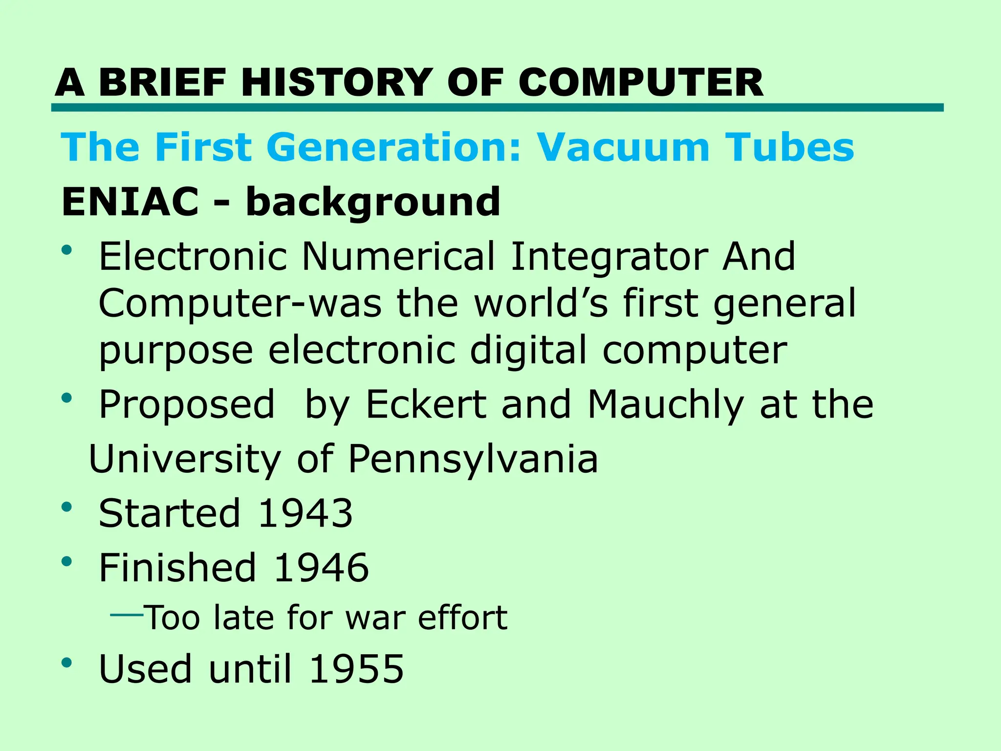
A BRIEF HISTORYOF COMPUTER
The First Generation: Vacuum Tubes
ENIAC - background
• Electronic Numerical Integrator And
Computer-was the world’s first general
purpose electronic digital computer
• Proposed by Eckert and Mauchly at the
University of Pennsylvania
• Started 1943
• Finished 1946
—Too late for war effort
• Used until 1955
3.
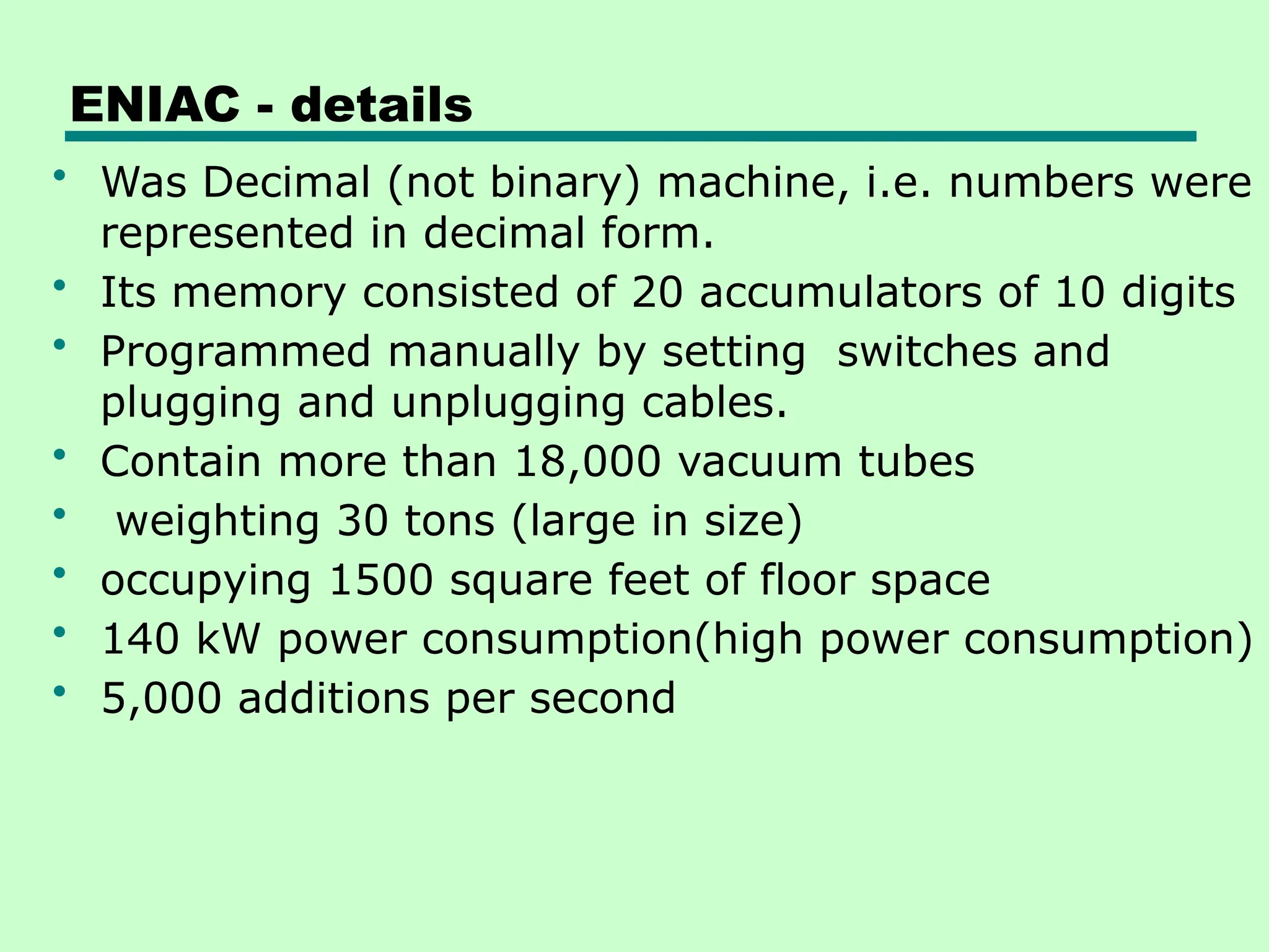
ENIAC - details
•Was Decimal (not binary) machine, i.e. numbers were
represented in decimal form.
• Its memory consisted of 20 accumulators of 10 digits
• Programmed manually by setting switches and
plugging and unplugging cables.
• Contain more than 18,000 vacuum tubes
• weighting 30 tons (large in size)
• occupying 1500 square feet of floor space
• 140 kW power consumption(high power consumption)
• 5,000 additions per second
4.
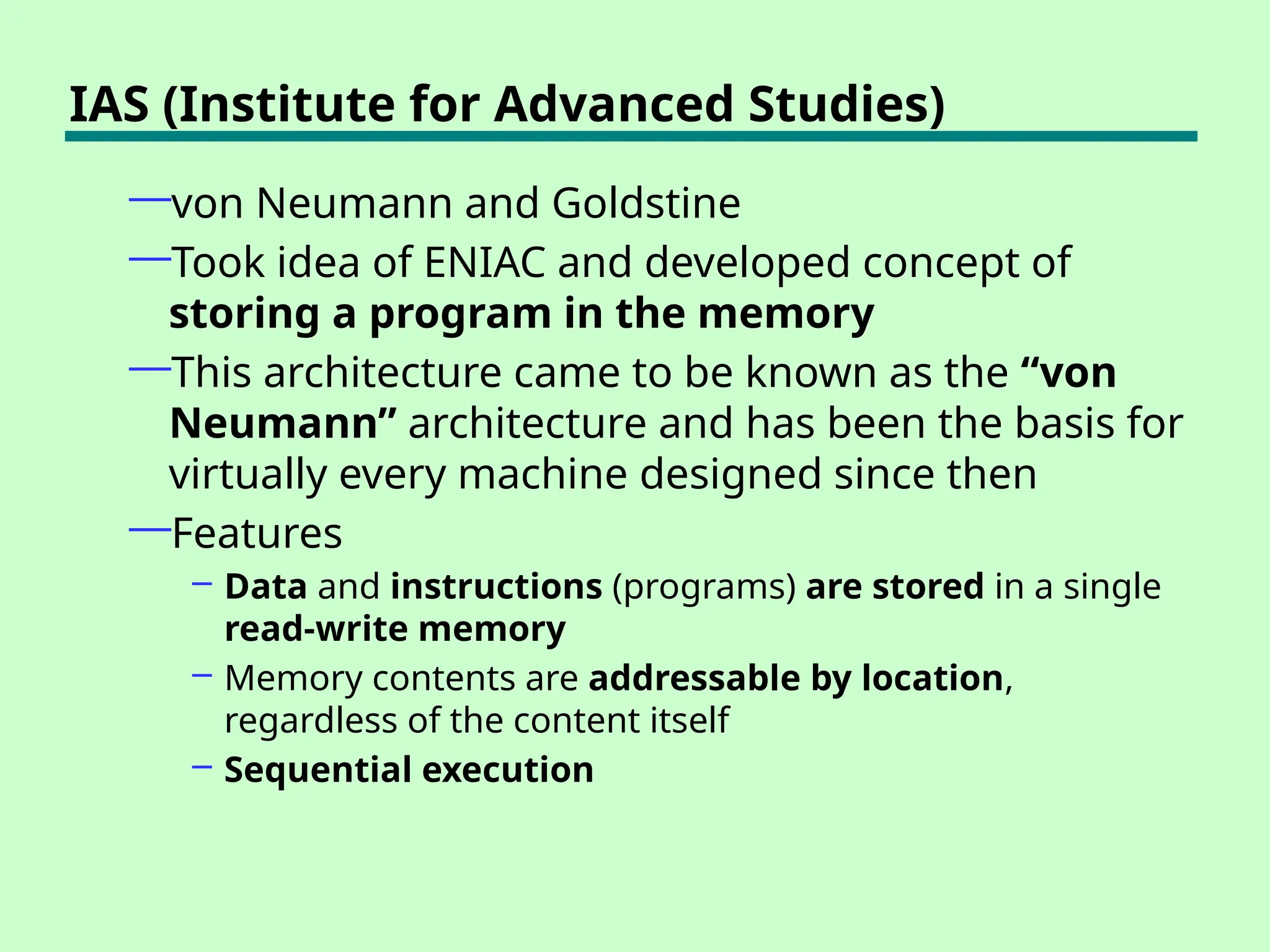
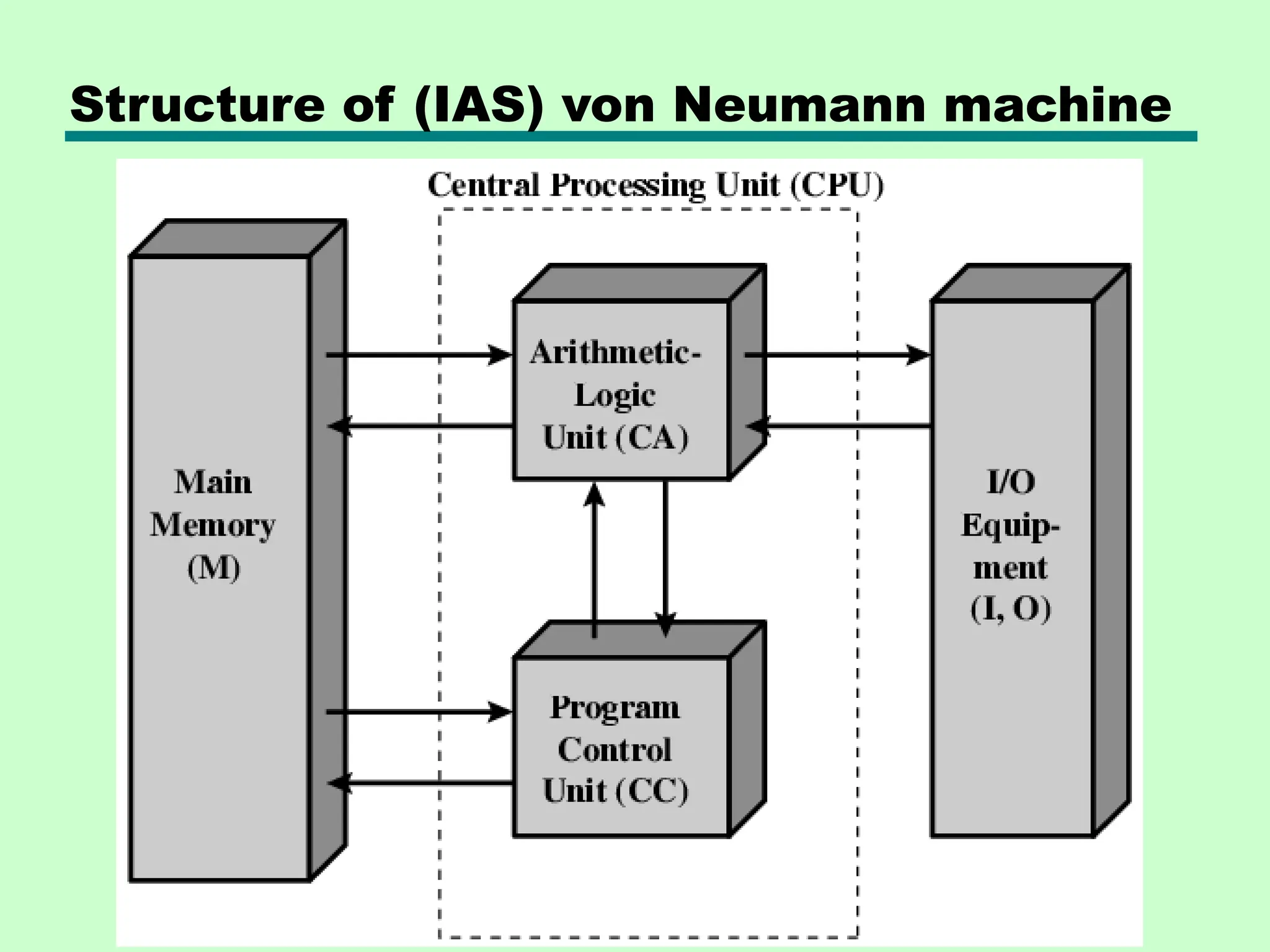
IAS (Institute forAdvanced Studies)
—von Neumann and Goldstine
—Took idea of ENIAC and developed concept of
storing a program in the memory
—This architecture came to be known as the “von
Neumann” architecture and has been the basis for
virtually every machine designed since then
—Features
– Data and instructions (programs) are stored in a single
read-write memory
– Memory contents are addressable by location,
regardless of the content itself
– Sequential execution
5.
von Neumann/Turing
• StoredProgram concept introduced in the late
1940s by John von Neumann
• Storage of instructions in computer memory to
enable it to perform a variety of tasks
• Main memory storing programs and data
• ALU operating on binary data
• Control unit interpreting instructions from
memory and executing
• Input and output equipment operated by control
unit
• Von Neumann began the design of a new stored
program computer referred to as the
IAS(Institute for Advanced Studies) computer
• IAS was Completed in 1952
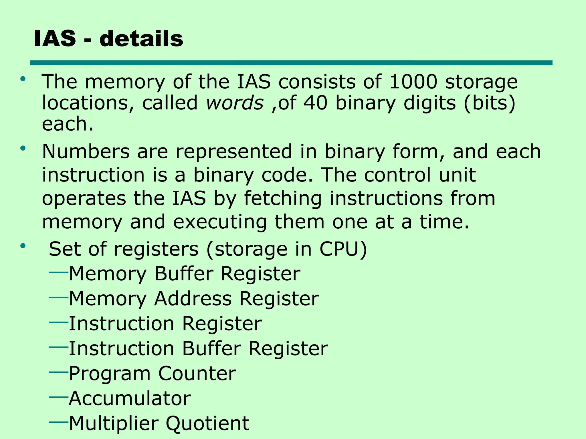
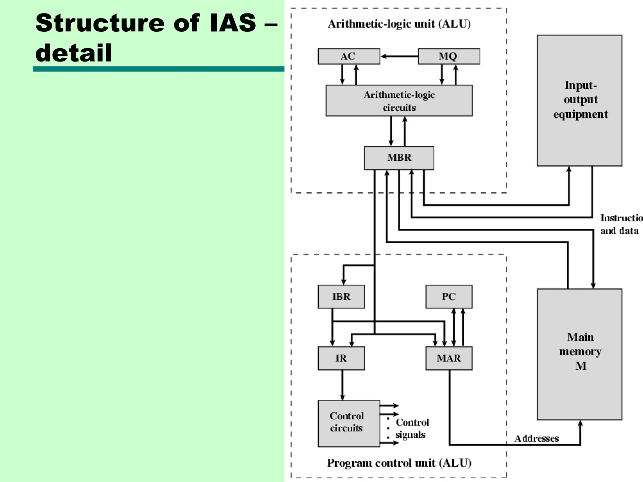
IAS - details
•The memory of the IAS consists of 1000 storage
locations, called words ,of 40 binary digits (bits)
each.
• Numbers are represented in binary form, and each
instruction is a binary code. The control unit
operates the IAS by fetching instructions from
memory and executing them one at a time.
• Set of registers (storage in CPU)
—Memory Buffer Register
—Memory Address Register
—Instruction Register
—Instruction Buffer Register
—Program Counter
—Accumulator
—Multiplier Quotient
8.
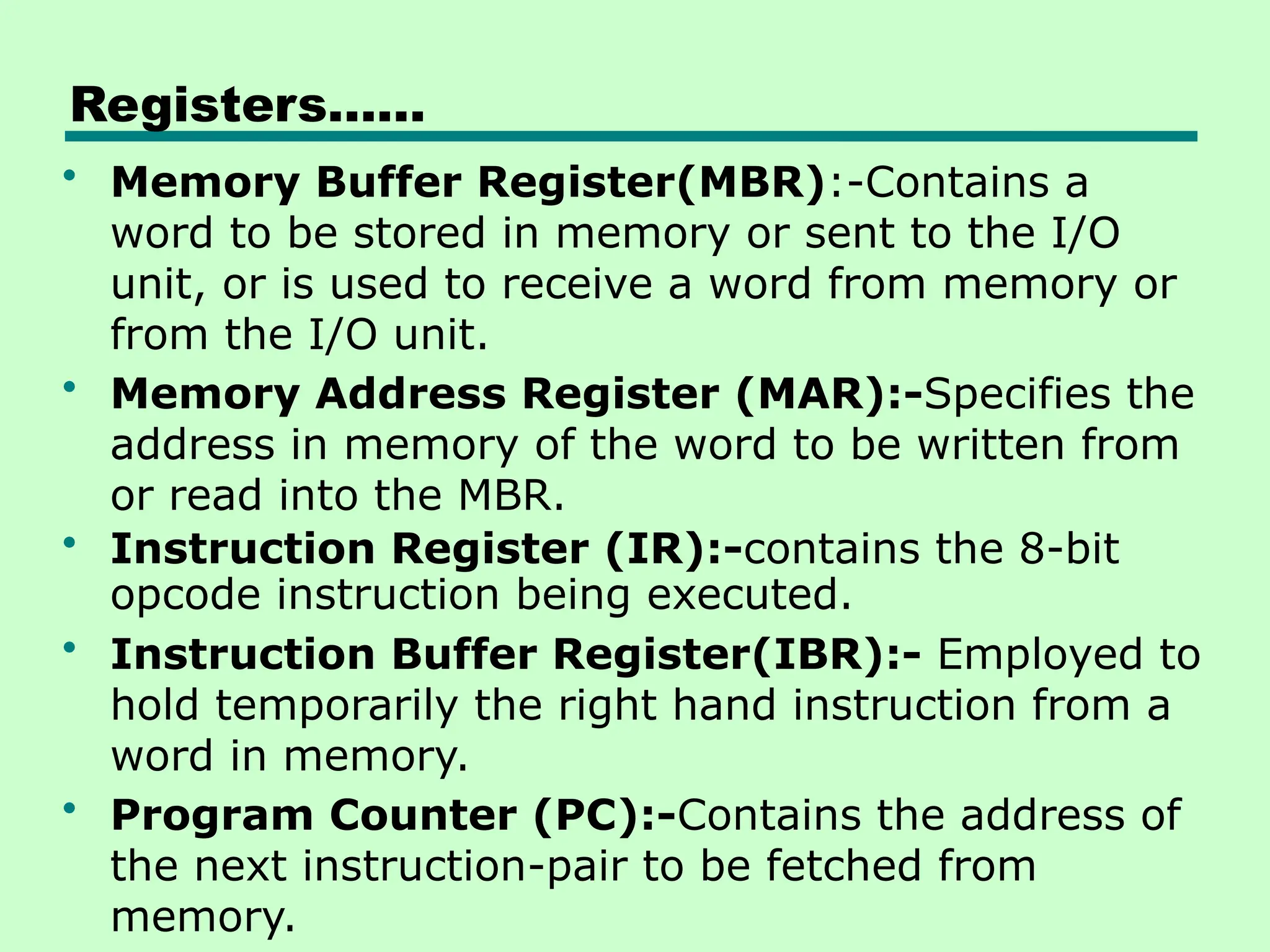
Registers……
• Memory BufferRegister(MBR):-Contains a
word to be stored in memory or sent to the I/O
unit, or is used to receive a word from memory or
from the I/O unit.
• Memory Address Register (MAR):-Specifies the
address in memory of the word to be written from
or read into the MBR.
• Instruction Register (IR):-contains the 8-bit
opcode instruction being executed.
• Instruction Buffer Register(IBR):- Employed to
hold temporarily the right hand instruction from a
word in memory.
• Program Counter (PC):-Contains the address of
the next instruction-pair to be fetched from
memory.
9.
Registers…
• Accumulator (AC)and multiplier quotient (MQ):
Employed to hold temporarily operands and results of
ALU operations. For example, the result of multiplying
two 40-bit numbers is an 80-bit number; the most
significant 40 bits are stored in the AC and the least
significant in the MQ.
• The IAS operates by repetitively performing an
instruction cycle.
• Each instruction cycle consists of two sub cycles.
During the fetch cycle, the opcode of the next
instruction is loaded into the IR and the address
portion is loaded into the MAR. This instruction may
be taken from the IBR, or it can be obtained from
memory by loading a word into the MBR, and then
down to the IBR, IR, and MAR.
Commercial Computers
• The1950s saw the birth of the computer
industry with two companies, Sperry and IBM,
dominating the marketplace.
• 1947- UNIVAC I (Universal Automatic
Computer) was the first successful
commercial computer
—It was intended for both scientific and commercial
applications.
• Late 1950s - UNIVAC II
—greater memory capacity and higher performance
than the UNIVAC I
12.
IBM
• BM, themajor manufacturer of punched-
card processing equipment, delivered its
first electronic stored-program computer
• 1953 - the 701
—IBM’s first stored program computer
—Intended for Scientific calculations
• 1955 - the 702
—For Business applications
• Lead to 700/7000 series
13.
2nd
generation: Transistors
• Replacedvacuum tubes
• Smaller
• Cheaper
• Less heat dissipation
• Solid State device
• Made from Silicon (Sand)
• Invented 1947 at Bell Labs
—Technology change
— Transistors
— High level languages
— Floating point arithmetic
14.
Transistor Based Computers
•Second generation machines
• NCR & RCA were the front-runners with
some small transistor machines.
• IBM followed shortly with the 7000 series.
• DEC - 1957
—Produced PDP-1
15.
3rd
generation: Integrated Circuits
•Throughout the 1950s and early 1960s, electronic
equipment was composed largely of discrete
components—transistors, resistors, capacitors, etc
• Discrete components were manufactured
separately, packaged in their own containers
• The entire manufacturing process, from transistor
to circuit board, was expensive and cumbersome
• These facts of life were beginning to create
problems in the computer industry.
• In 1958 came the achievement that revolutionized
electronics and started the era of
microelectronics: the invention of the integrated
circuit.
16.
Microelectronics
• Means Literally- “small electronics”
• A computer is made up of gates, memory cells
and interconnections
• A gate is a device that implements a simple
Boolean or logical function.
• The memory cell is a device that can store one
bit of data
• These can be manufactured on a semiconductor
• e.g. silicon wafer
• the two most important members of the third
generation computers were:
—the IBM System/360
— the DEC PDP-8.
17.
IBM 360 series
•By 1964
• Replaced (& not compatible with) 7000 series
• The System/360 was the industry’s first planned
family of computers.
• The characteristics of a family are as follows:
—Similar or identical instruction set: In many cases,
the exact same set of machine instructions is supported
on all members of the family. Thus, a program that
executes on one machine will also execute on any other.
In some cases, the lower end of the family has an
instruction set that is a subset of that of the top end of
the family.
— Similar or identical operating system: The same
basic operating system is available for all family
members. In some cases, additional features are added
to the higher-end members.
18.
The characteristics of. . .
—Increasing speed: The rate of instruction execution
increases in going from lower to higher family
members.
—Increasing number of I/O ports: The number of I/O
ports increases in going from lower to higher family
members.
— Increasing memory size: The size of main memory
increases in going from lower to higher family
members.
—Increasing cost: At a given point in time, the cost of a
system increases in going from lower to higher family
members.
19.
DEC PDP-8
• ThePDP-8 (Programmed Data Processor) was
introduced in 1965 by Digital Equipment
Corporation (DEC).
• It is the first minicomputer
• Did not need air conditioned room
• Small enough to sit on a lab bench
• $16,000
—$100k+ for IBM 360
• Embedded applications & OEM
• Use BUS STRUCTURE- Omnibus
20.
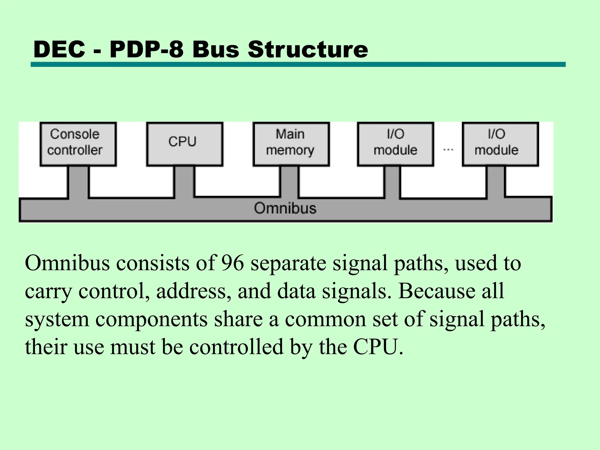
DEC - PDP-8Bus Structure
Omnibus consists of 96 separate signal paths, used to
carry control, address, and data signals. Because all
system components share a common set of signal paths,
their use must be controlled by the CPU.
21.
Larger Generations
• Beyondthe third generation there is less general
agreement on defining generations of computers.
• Large scale integration - 1971-1977
—3,000 - 100,000 components on a chip
• Very large scale integration - 1978 -1991
—100,000 - 100,000,000 components on a chip
• Ultra large scale integration – 1991 -
—Over 100,000,000 components on a chip
• two of the most important of these results
—Semi conductor memory
—Microprocessor
22.
Semiconductor Memory
• Thefirst application of integrated circuit technology
to computers was construction of the processor (the
control unit and the arithmetic and logic unit) out of
integrated circuit chips. But it was also found that
this same technology could be used to construct
memories.
• In 1970, Fairchild produced the first relatively
capacious semiconductor memory.
• Since 1970, semiconductor memory has been
through 13 generations: 1K, 4K,16K, 64K, 256K,
1M, 4M, 16M, 64M, 256M, 1G, 4G, and, as of this
writing, 16 Gbits on a single chip.
23.
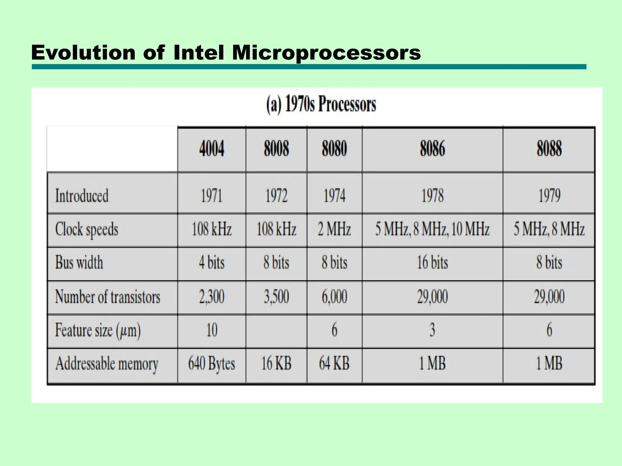
MICROPROCESSORS
• in 1971,Intel developed its 4004.
• The 4004 was the first chip to contain all of the
components of a CPU on a single chip.
• The 4004 can add two 4-bit numbers and can
multiply only by repeated addition
• The evolution of microprocessor can be seen
most easily in the number of bits that the
processor deals with at a time
• Data bus width of a processor : the number of
bits of data that can be brought into or sent out of
the processor at a time.
• The next major step in the evolution of the
microprocessor was the introduction in 1972 of the
Intel 8008.
24.
MICROPROCESSORS - --
• 8008 was the first 8-bit microprocessor and was
almost twice as complex as the 4004.
• in 1974 , the introduction of Intel 8080
• This was the first general-purpose microprocessor
• Whereas the 4004 and the 8008 had been
designed for specific applications, the 8080 was
designed to be the CPU of a general-purpose
microcomputer.
• The 8080 is faster, has a richer instruction set, and
has a large addressing capability.
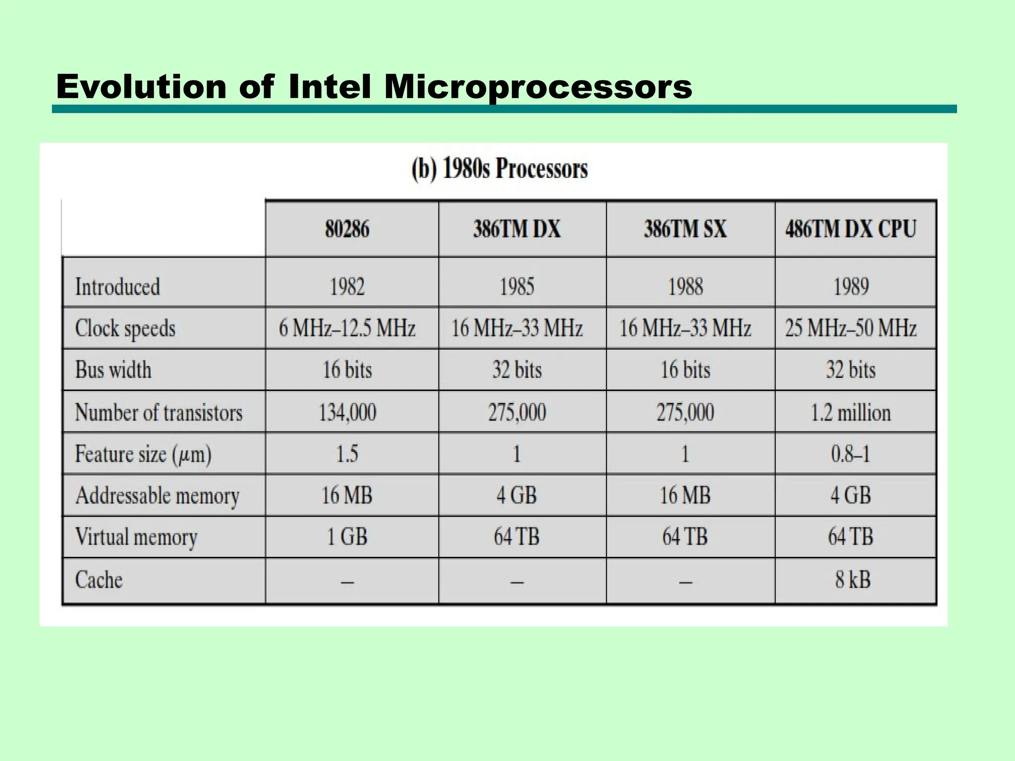
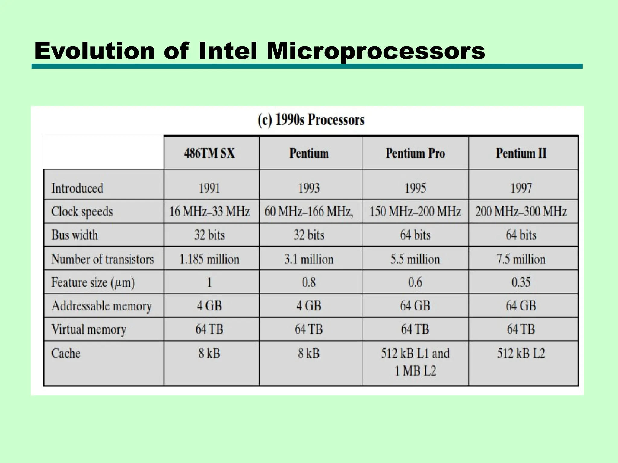
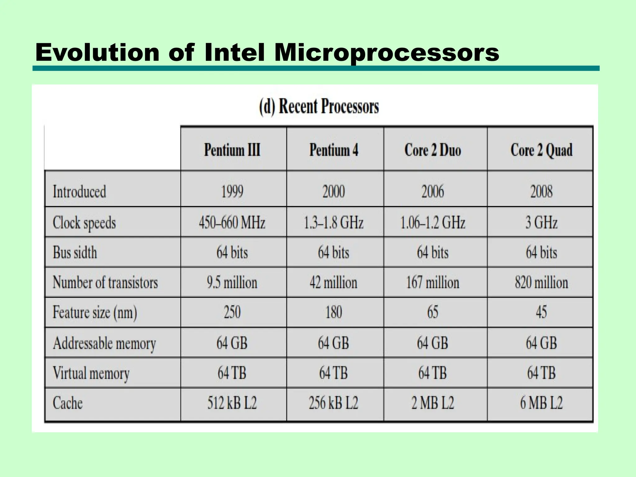
• The table below shows the Evolution of Intel
Microprocessors
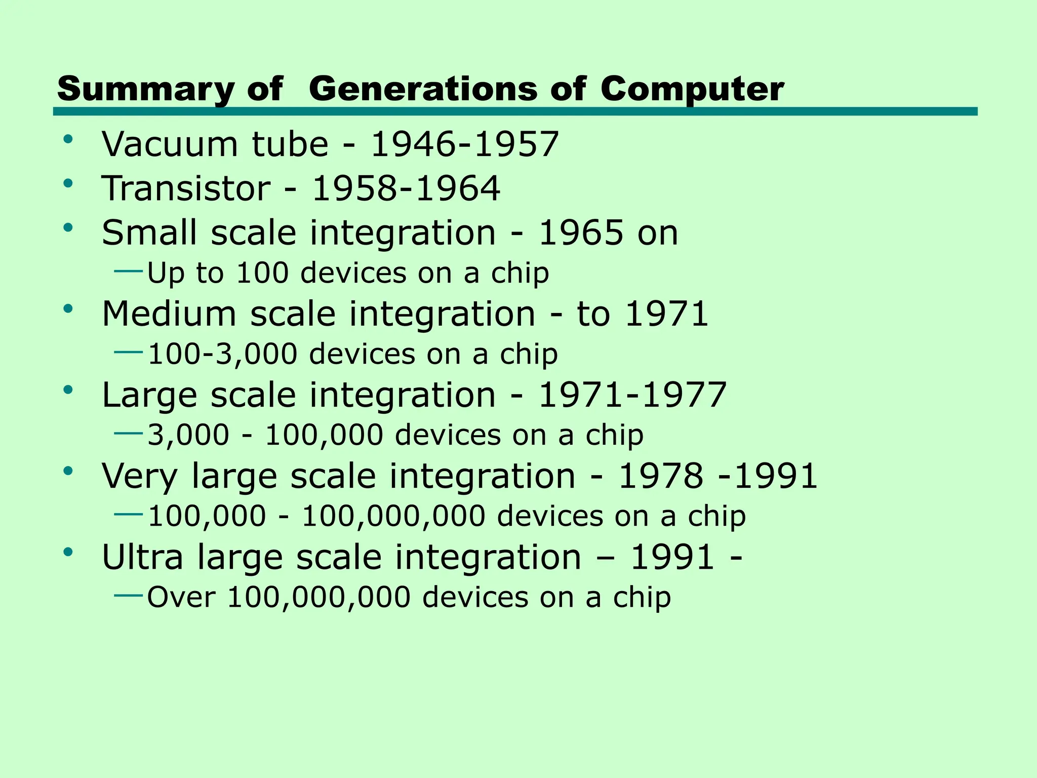
Summary of Generationsof Computer
• Vacuum tube - 1946-1957
• Transistor - 1958-1964
• Small scale integration - 1965 on
—Up to 100 devices on a chip
• Medium scale integration - to 1971
—100-3,000 devices on a chip
• Large scale integration - 1971-1977
—3,000 - 100,000 devices on a chip
• Very large scale integration - 1978 -1991
—100,000 - 100,000,000 devices on a chip
• Ultra large scale integration – 1991 -
—Over 100,000,000 devices on a chip
30.
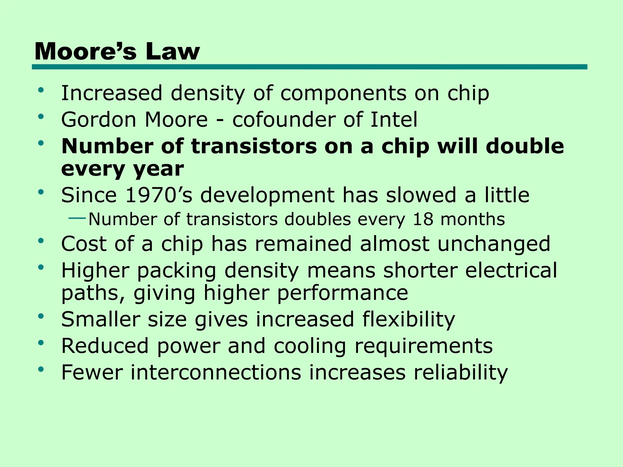
Moore’s Law
• Increaseddensity of components on chip
• Gordon Moore - cofounder of Intel
• Number of transistors on a chip will double
every year
• Since 1970’s development has slowed a little
—Number of transistors doubles every 18 months
• Cost of a chip has remained almost unchanged
• Higher packing density means shorter electrical
paths, giving higher performance
• Smaller size gives increased flexibility
• Reduced power and cooling requirements
• Fewer interconnections increases reliability
31.
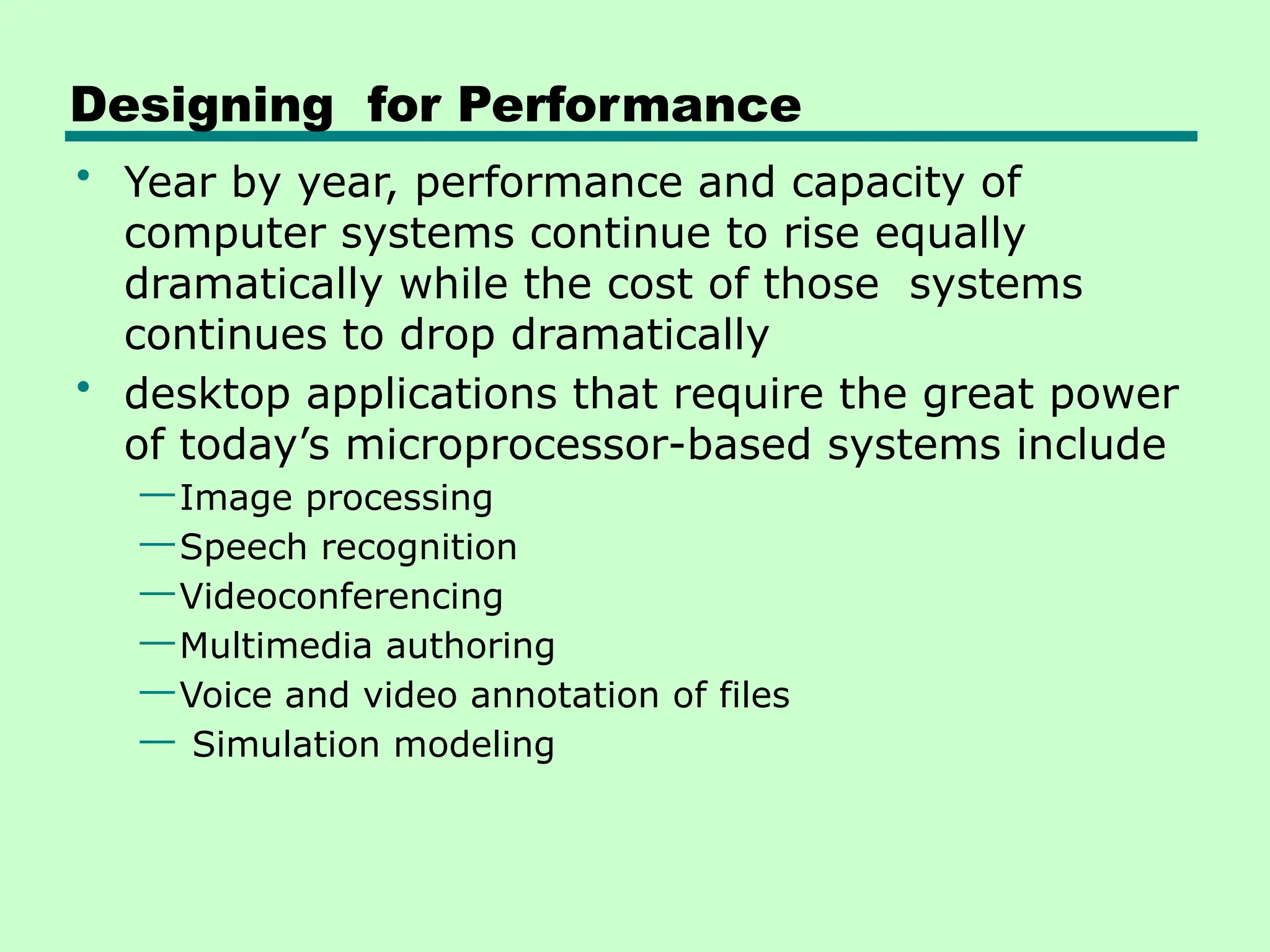
Designing for Performance
•Year by year, performance and capacity of
computer systems continue to rise equally
dramatically while the cost of those systems
continues to drop dramatically
• desktop applications that require the great power
of today’s microprocessor-based systems include
—Image processing
—Speech recognition
—Videoconferencing
—Multimedia authoring
—Voice and video annotation of files
— Simulation modeling
32.
Microprocessor speed
• chipmakerscan unleash a new generation of
chips every three years—with four times as many
transistors.
• in microprocessors, the addition of new circuits,
and the speed boost that comes from reducing
the distances between them, has improved
performance four or five fold every three years or
so since Intel launched its x86 family in 1978.
• But the raw speed of the microprocessor will not
achieve its potential unless it is fed a constant
stream of work to do in the form of computer
instructions.
33.
Microprocessor speed
• whilethe chipmakers have been busy learning
how to fabricate chips of greater and greater
density, the processor designers must come up
with ever more elaborate techniques for feeding
the monster (i.e to exploit the raw speed of the
processor).
• Among the techniques built into contemporary
processors are the following:
—Pipelining
—On board L1 & L2 cache
—Branch prediction
—Data flow analysis
—Speculative execution
34.
Microprocessor speed
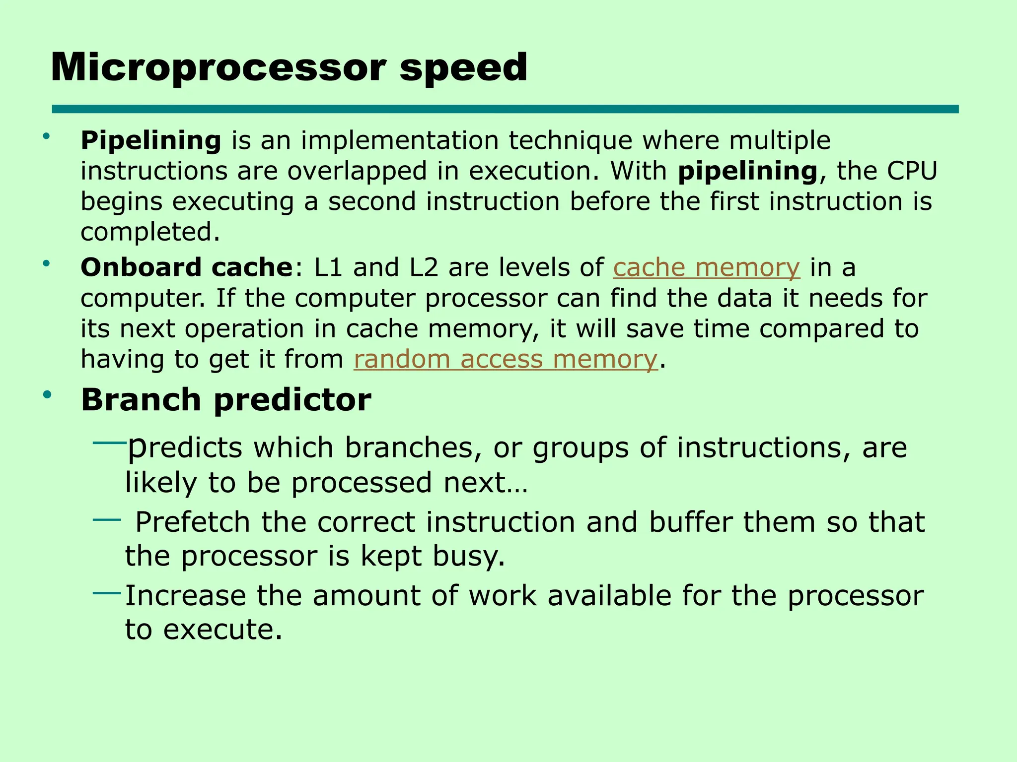
• Pipeliningis an implementation technique where multiple
instructions are overlapped in execution. With pipelining, the CPU
begins executing a second instruction before the first instruction is
completed.
• Onboard cache: L1 and L2 are levels of cache memory in a
computer. If the computer processor can find the data it needs for
its next operation in cache memory, it will save time compared to
having to get it from random access memory.
• Branch predictor
—predicts which branches, or groups of instructions, are
likely to be processed next…
— Prefetch the correct instruction and buffer them so that
the processor is kept busy.
—Increase the amount of work available for the processor
to execute.
35.
Microprocessor Speed
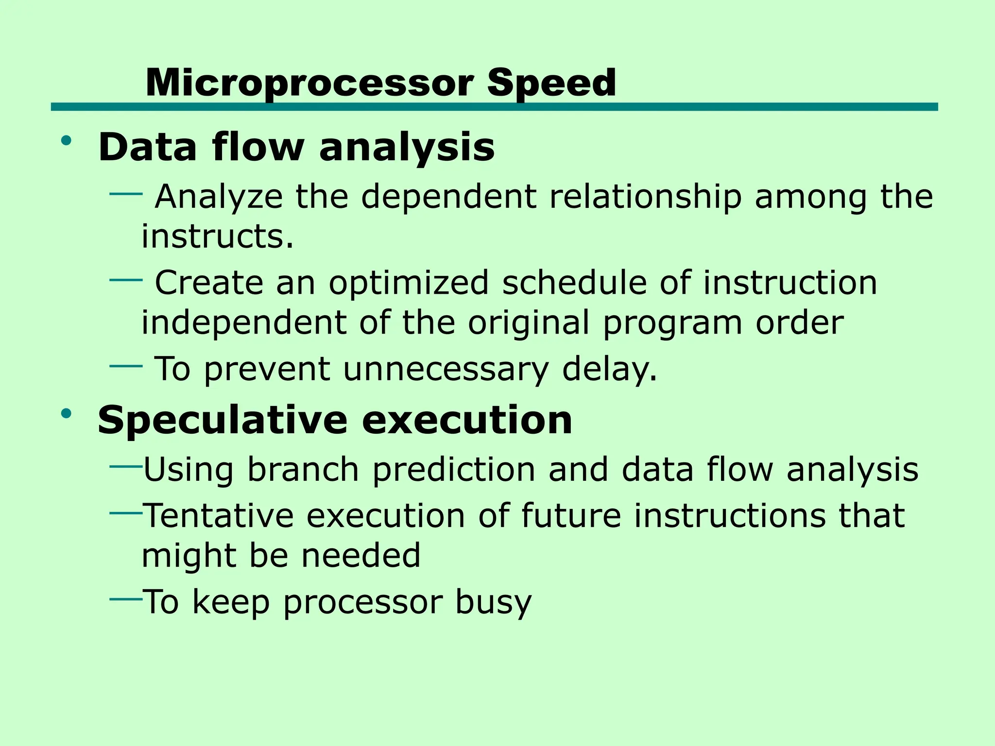
• Dataflow analysis
— Analyze the dependent relationship among the
instructs.
— Create an optimized schedule of instruction
independent of the original program order
— To prevent unnecessary delay.
• Speculative execution
—Using branch prediction and data flow analysis
—Tentative execution of future instructions that
might be needed
—To keep processor busy
36.
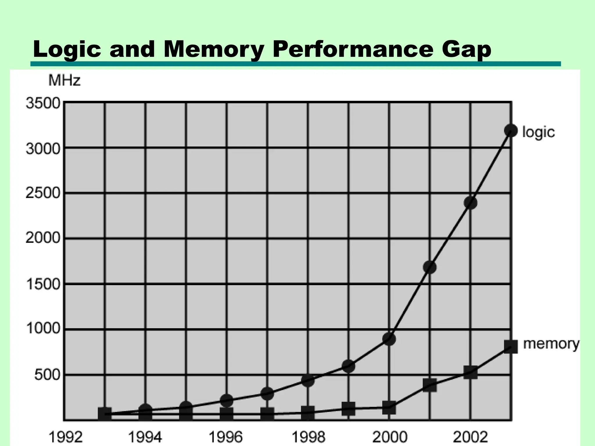
Performance Balance
• Processorspeed increased
• Memory capacity increased
• The speed with which data can be transferred
between main memory and the processor has lagged
badly(i.e. Memory speed lags behind processor
speed)
• The interface between processor and main memory
is the most crucial pathway in the entire Computer
because it is responsible for carrying a constant flow
of program instructions and data between memory
chips and the processor.
• If memory or the pathway fails to keep pace with the
processor’s insistent demands, the processor stalls in
a wait state, and valuable processing time is lost.
Solutions
• Increase numberof bits retrieved at one time by
making DRAMs “wider” rather than “deeper” and
by using wide bus data paths
• Change the DRAM interface to make it more
efficient by including a cache or other buffering
scheme on the DRAM chip.
• Reduce frequency of memory access
—More complex cache and cache on chip
• Increase interconnection bandwidth by using
—High speed buses
—Hierarchy of buses
39.
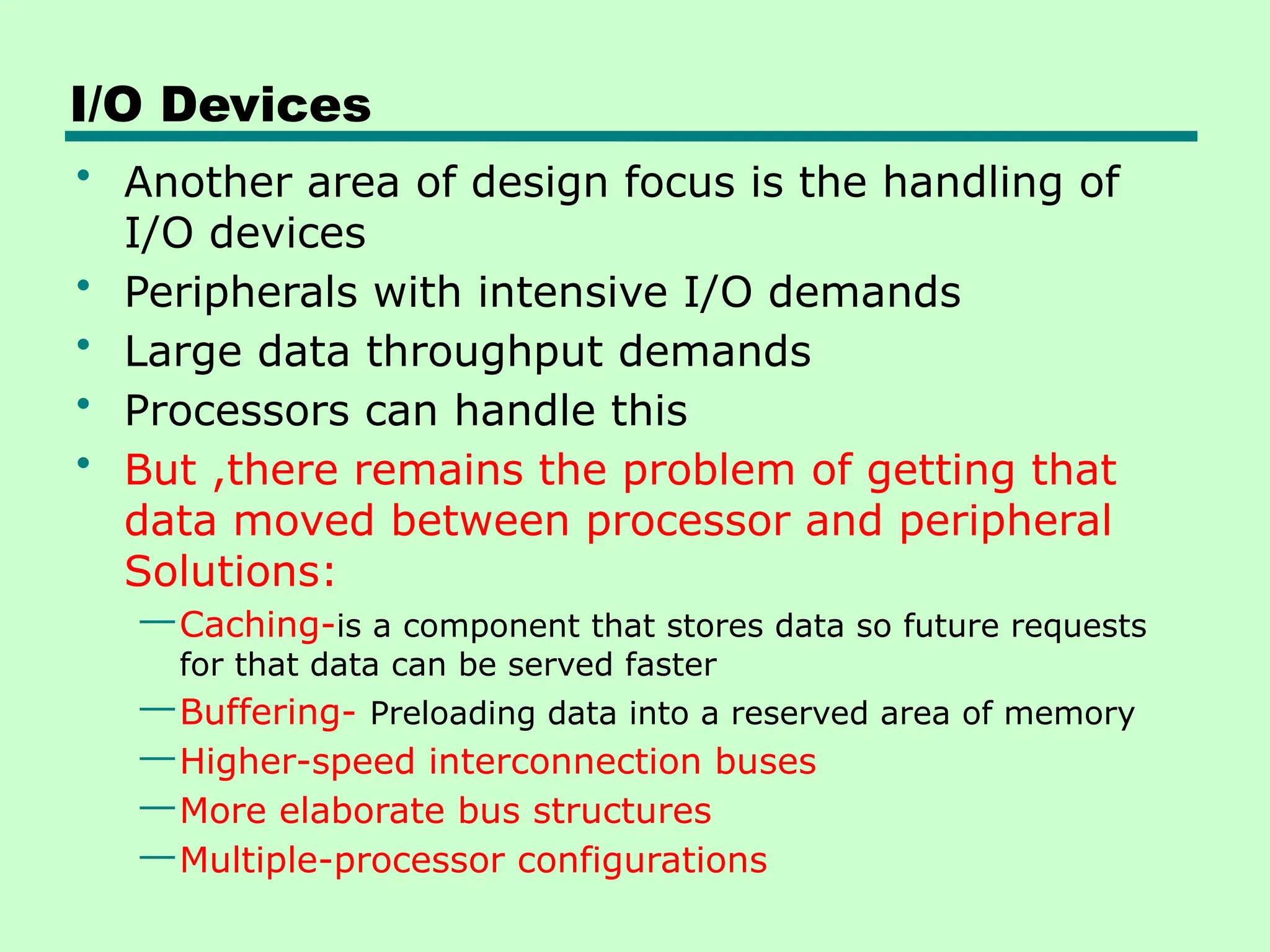
I/O Devices
• Anotherarea of design focus is the handling of
I/O devices
• Peripherals with intensive I/O demands
• Large data throughput demands
• Processors can handle this
• But ,there remains the problem of getting that
data moved between processor and peripheral
Solutions:
—Caching-is a component that stores data so future requests
for that data can be served faster
—Buffering- Preloading data into a reserved area of memory
—Higher-speed interconnection buses
—More elaborate bus structures
—Multiple-processor configurations
40.
Key is Balance
•Designers constantly strive to balance the
throughput and processing demands of the
—Processor components
—Main memory
—I/O devices
—Interconnection structures
41.
Improvements in ChipOrganization and
Architecture
• There are three approaches to achieving increased processor
speed
• Increase hardware speed of processor
—Fundamentally due to shrinking logic gate size on CPU
—More gates can be packed together more tightly and to
increasing the clock rate.
—With gates closer together, the propagation time for signals
is significantly reduced, enabling a speeding up of the
processor.
—An increase in clock rate means that individual
operations are executed more rapidly.
• Increase size and speed of caches
• Change processor organization and architecture
—Increase effective speed of execution
—Parallelism
42.
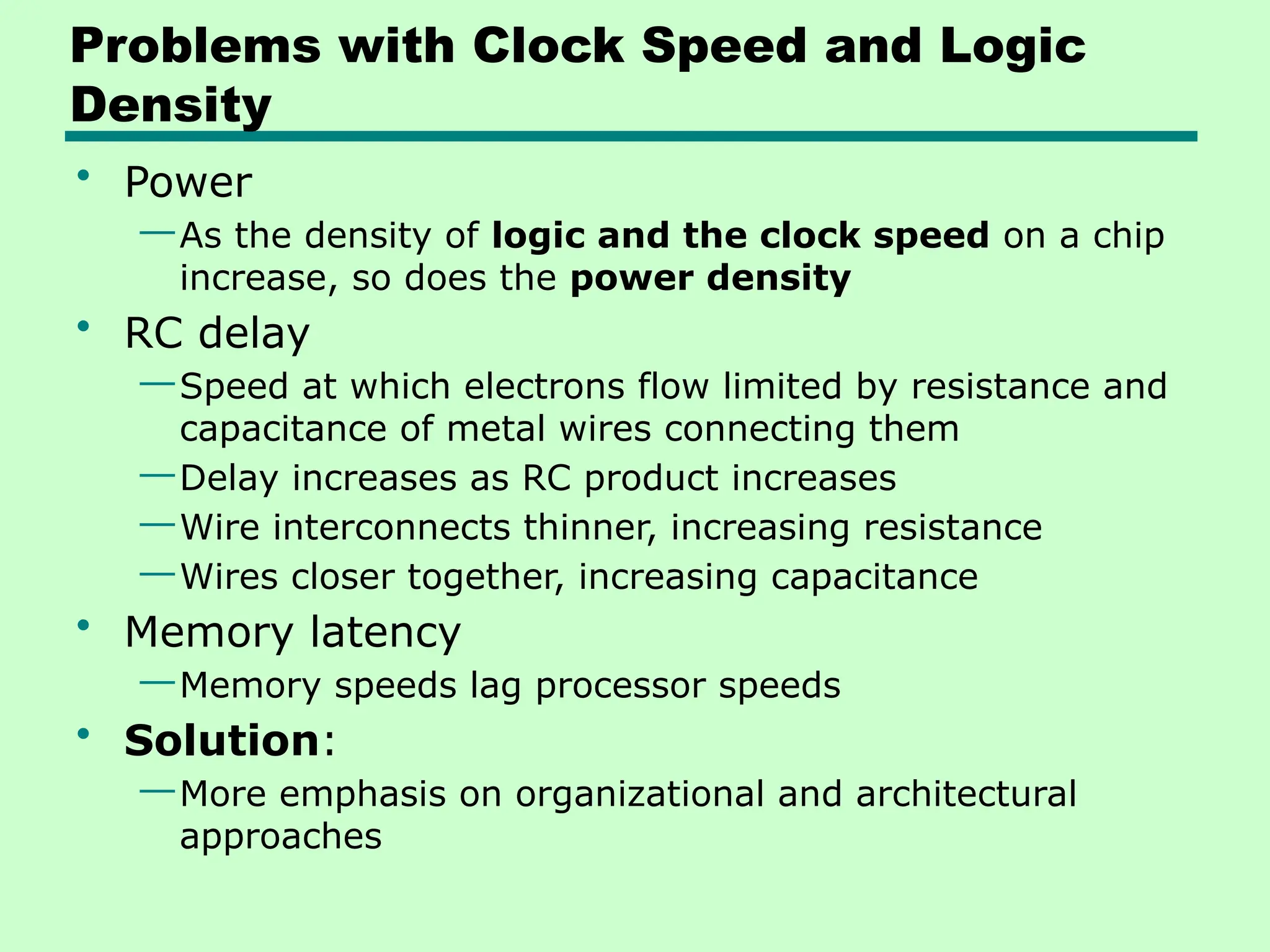
Problems with ClockSpeed and Logic
Density
• Power
—As the density of logic and the clock speed on a chip
increase, so does the power density
• RC delay
—Speed at which electrons flow limited by resistance and
capacitance of metal wires connecting them
—Delay increases as RC product increases
—Wire interconnects thinner, increasing resistance
—Wires closer together, increasing capacitance
• Memory latency
—Memory speeds lag processor speeds
• Solution:
—More emphasis on organizational and architectural
approaches
Intel microprocessor performance
•In late 1980s, two main strategies have been
used to increase performance beyond what can
be achieved simply by increasing clock speed.
• First , there has been an increase in cache
Capacity,
• Secondly, the instruction execution logic within a
processor has become increasingly complex to
enable parallel execution of instructions within
processor.
45.
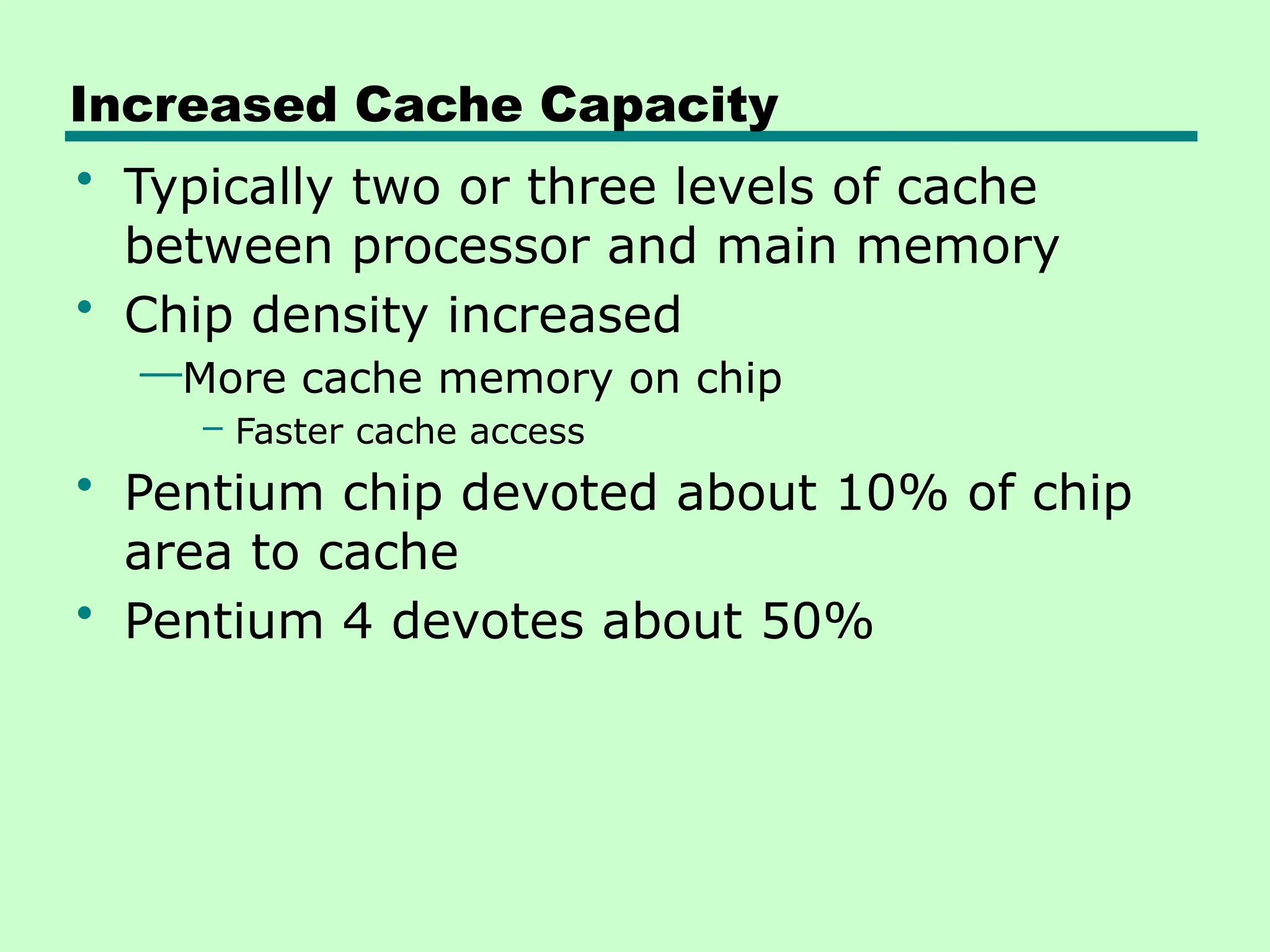
Increased Cache Capacity
•Typically two or three levels of cache
between processor and main memory
• Chip density increased
—More cache memory on chip
– Faster cache access
• Pentium chip devoted about 10% of chip
area to cache
• Pentium 4 devotes about 50%
46.
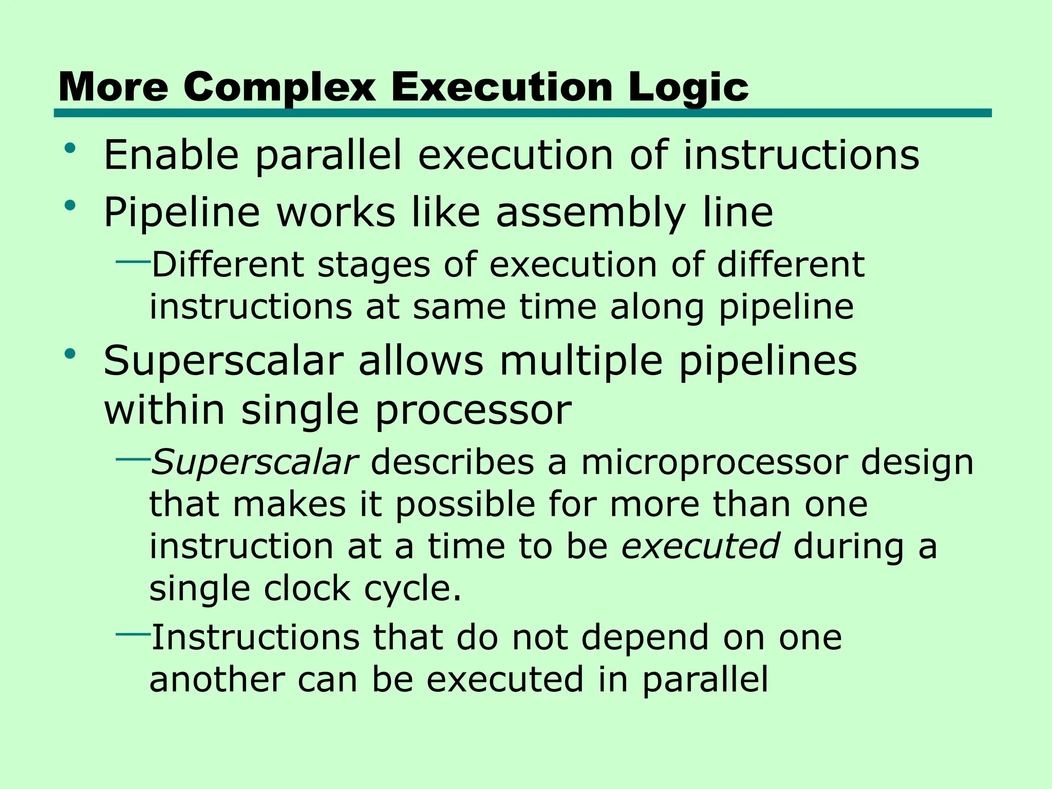
More Complex ExecutionLogic
• Enable parallel execution of instructions
• Pipeline works like assembly line
—Different stages of execution of different
instructions at same time along pipeline
• Superscalar allows multiple pipelines
within single processor
—Superscalar describes a microprocessor design
that makes it possible for more than one
instruction at a time to be executed during a
single clock cycle.
—Instructions that do not depend on one
another can be executed in parallel
47.
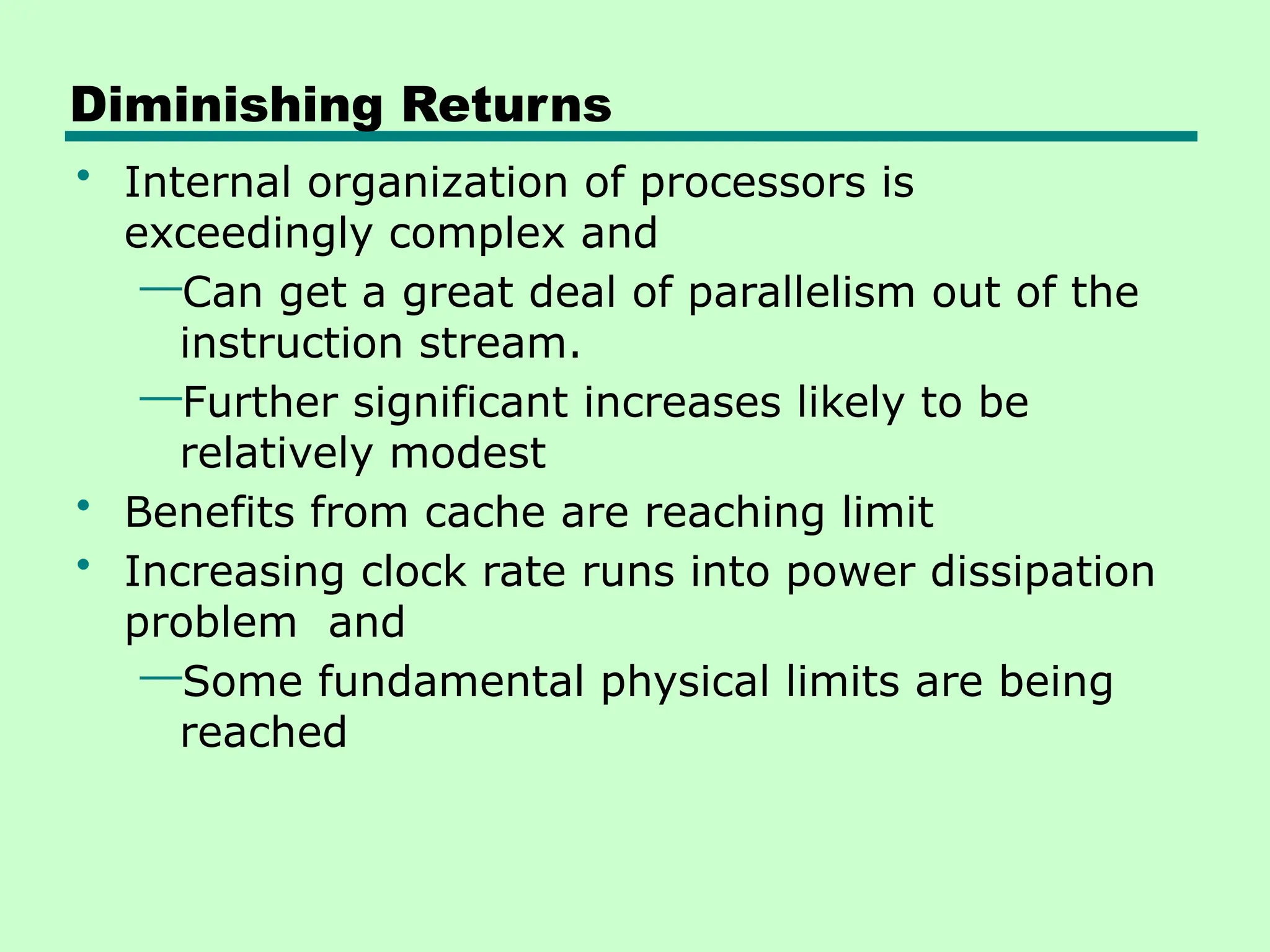
Diminishing Returns
• Internalorganization of processors is
exceedingly complex and
—Can get a great deal of parallelism out of the
instruction stream.
—Further significant increases likely to be
relatively modest
• Benefits from cache are reaching limit
• Increasing clock rate runs into power dissipation
problem and
—Some fundamental physical limits are being
reached
48.
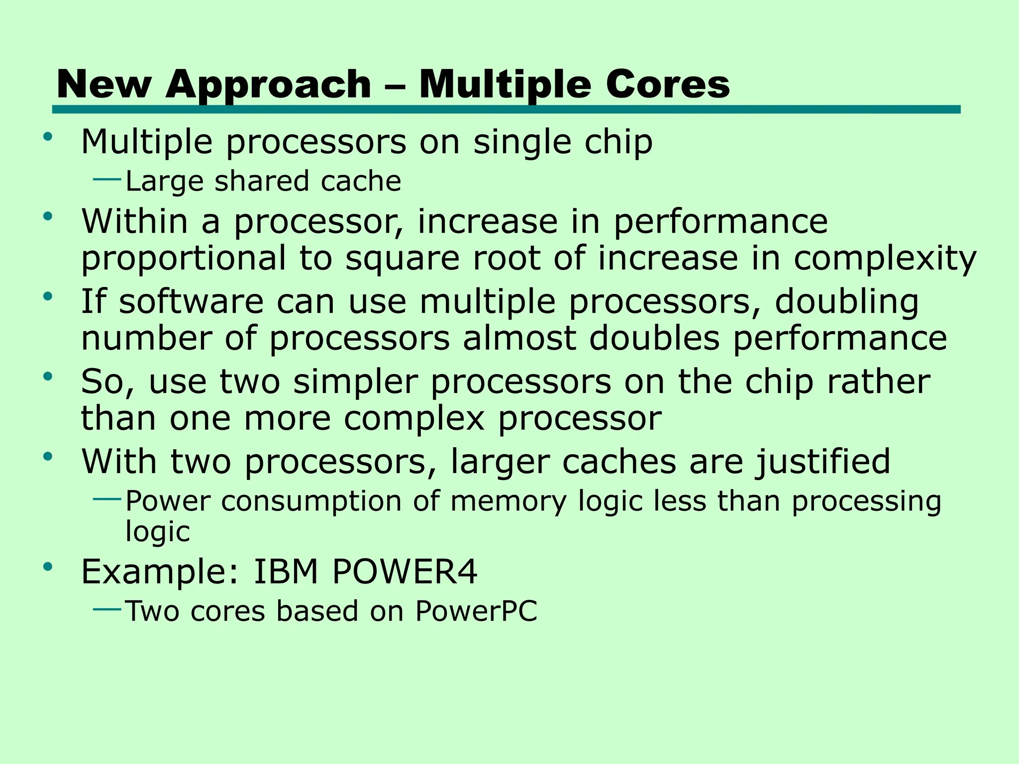
New Approach –Multiple Cores
• Multiple processors on single chip
—Large shared cache
• Within a processor, increase in performance
proportional to square root of increase in complexity
• If software can use multiple processors, doubling
number of processors almost doubles performance
• So, use two simpler processors on the chip rather
than one more complex processor
• With two processors, larger caches are justified
—Power consumption of memory logic less than processing
logic
• Example: IBM POWER4
—Two cores based on PowerPC
49.
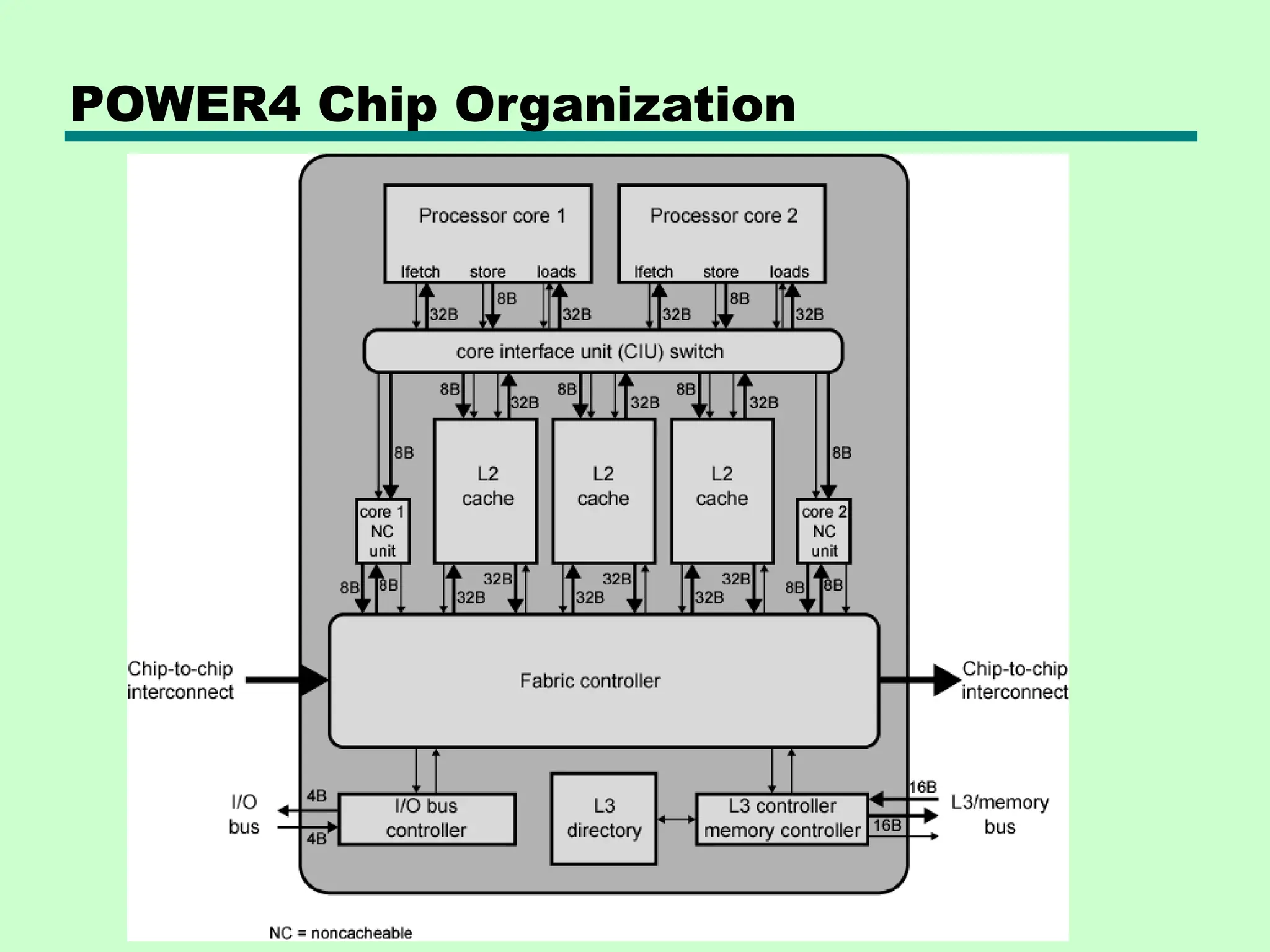
The POWER4 chip
•The POWER4 is a microprocessor developed by
International Business Machines (IBM) that implemented the
64-bit PowerPC and PowerPC AS instruction set architectures
• The POWER4 chip has a maximum of two microprocessors, each
of which is a fully functional 64-bit implementation of the
PowerPC AS Architecture specification
• Physically, there are three key components: the POWER4
processor chip, the L3 merged logic DRAM (MLD) chip and the
memory controller chip.
— The POWER4 processor chip has two 64-bit microprocessors, a microprocessor
interface controller unit, a 1.41-MB L2 cache, an L3 cache directory, a fabric
controller responsible for controlling the flow of data and controls on and off the
chip, and chip/system pervasive functions.
— The L3 MLD chip contains 16 MB of cache. Two such chips, mounted on their
own module, are used for the 32 MB of L3 attached to each POWER4 chip. An 8-
way POWER4 SMP module shares 128 MB of L3 cache.
— The memory controller chip features one or two memory data ports and
connects to the L3 MLD chips on one side and to the synchronous memory
interface (SMI) chips on the other.
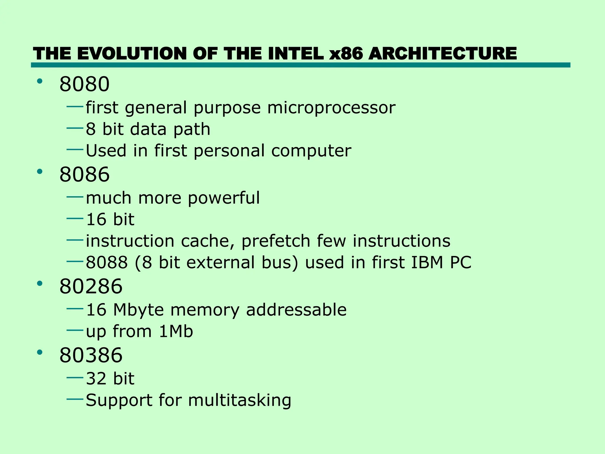
THE EVOLUTION OFTHE INTEL x86 ARCHITECTURE
• 8080
—first general purpose microprocessor
—8 bit data path
—Used in first personal computer
• 8086
—much more powerful
—16 bit
—instruction cache, prefetch few instructions
—8088 (8 bit external bus) used in first IBM PC
• 80286
—16 Mbyte memory addressable
—up from 1Mb
• 80386
—32 bit
—Support for multitasking
52.
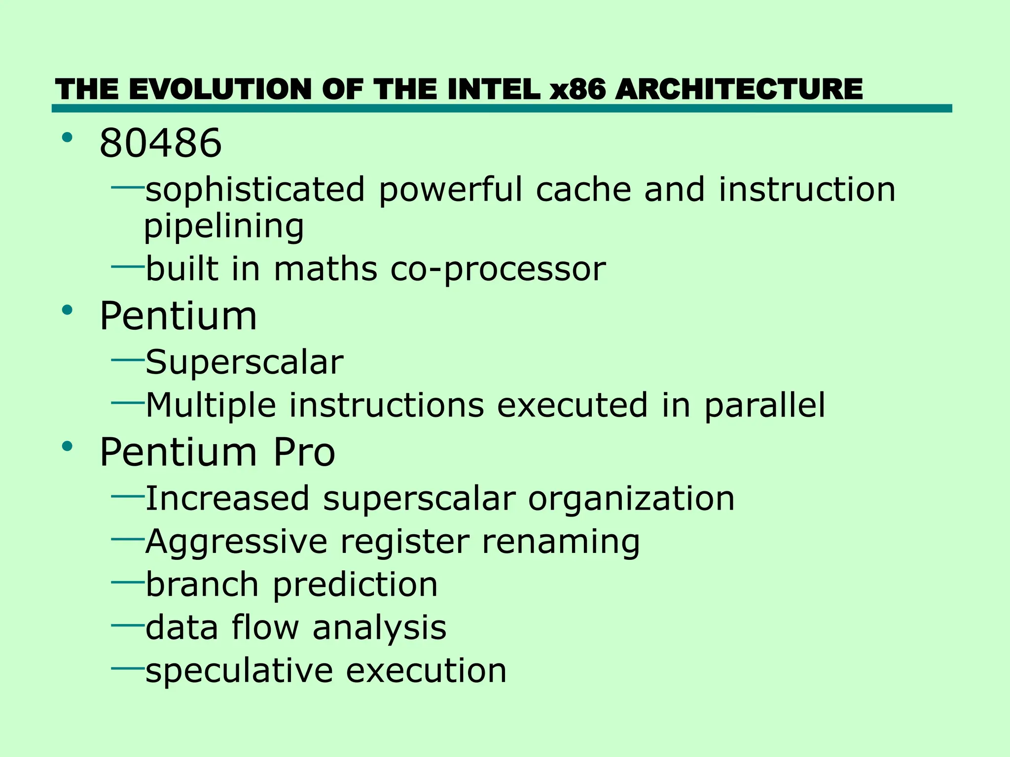
THE EVOLUTION OFTHE INTEL x86 ARCHITECTURE
• 80486
—sophisticated powerful cache and instruction
pipelining
—built in maths co-processor
• Pentium
—Superscalar
—Multiple instructions executed in parallel
• Pentium Pro
—Increased superscalar organization
—Aggressive register renaming
—branch prediction
—data flow analysis
—speculative execution
53.
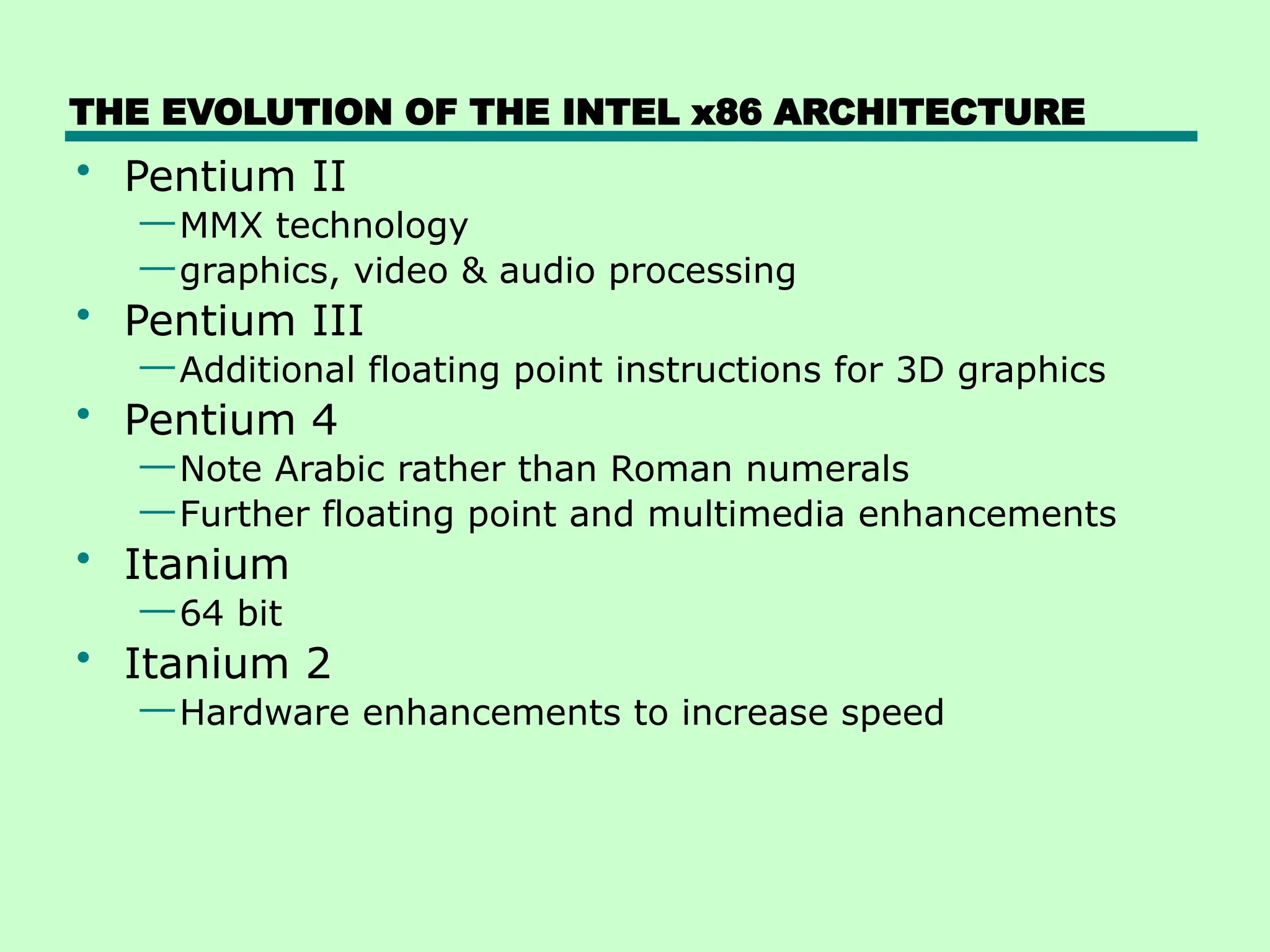
THE EVOLUTION OFTHE INTEL x86 ARCHITECTURE
• Pentium II
—MMX technology
—graphics, video & audio processing
• Pentium III
—Additional floating point instructions for 3D graphics
• Pentium 4
—Note Arabic rather than Roman numerals
—Further floating point and multimedia enhancements
• Itanium
—64 bit
• Itanium 2
—Hardware enhancements to increase speed
54.
THE EVOLUTION OFTHE INTEL x86 ARCHITECTURE
• Core
— First x86 with dual core,
— referring to the implementation of two processors on a single chip
• Core 2
— 64 bit architecture
— two processors on a single chip
• Core 2 Quad
—Four processors on chip
• x86 architecture dominant outside embedded
systems
• Organization and technology changed dramatically
• Instruction set architecture evolved with backwards
compatibility
55.
PowerPC
• PowerPC isa microprocessor architecture that was
developed jointly by Apple, IBM, and Motorola.
• 1986, IBM commercial RISC workstation product, RT PC.
— Not commercial success
— Many rivals with comparable or better performance
• 1990, IBM RISC System/6000
— RISC-like superscalar machine
— POWER architecture
• IBM alliance with Motorola (68000 microprocessors), and
Apple, (used 68000 in Macintosh)
• Result is PowerPC architecture
— Derived from the POWER architecture
— Superscalar RISC
— Apple Macintosh
— Embedded chip applications
56.
PowerPC Family
• 601:
—Quicklyto market. 32-bit machine
• 603:
—Low-end desktop and portable
—32-bit
—Comparable performance with 601
—Lower cost and more efficient implementation
• 604:
—Desktop and low-end servers
—32-bit machine
—Much more advanced superscalar design
—Greater performance
• 620:
—High-end servers
—64-bit architecture
57.
PowerPC Family
• 740/750:
—Alsoknown as G3
—Two levels of cache on chip
• G4:
—Increases parallelism and internal speed
• G5:
—Improvements in parallelism and internal
speed
—64-bit organization
Group Assignment (10%)
•For the following microprocessors
—8086,
—Dual core,
—Core i3 processors,
1. Explain the basic architecture and key
distinguishing features of each processor
2. Compare each microprocessor by bus
width ,number of transistor, addressable
memory, performance, cost,etc