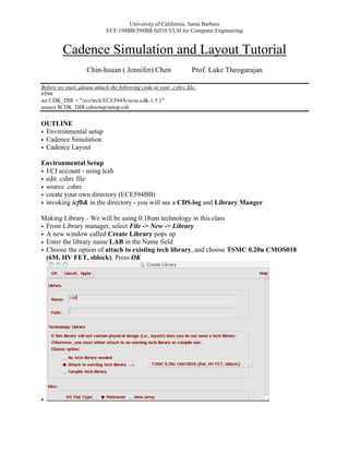
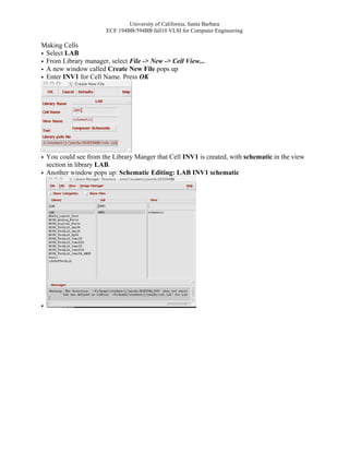
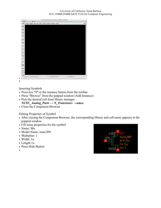
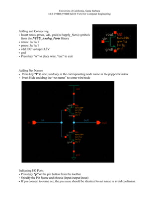
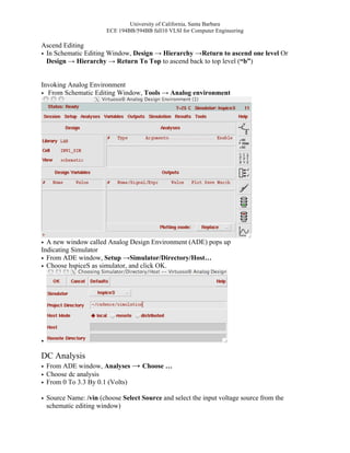
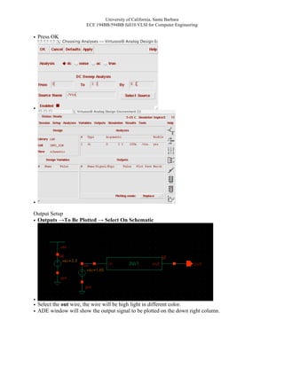
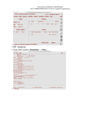
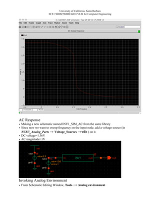
University of California, Santa Barbara
                             ECE 194BB/594BB fall10 VLSI for Computer Engineering


         Cadence Simulation and Layout Tutorial
                    Chin-hsuan ( Jennifer) Chen                     Prof. Luke Theogarajan

Before we start, please attach the following code in your .cshrc file:
#594
set CDK_DIR = "/eci/tech/ECE594A/ncsu-cdk-1.5.1"
source $CDK_DIR/cdssetup/setup.csh

OUTLINE
• Environmental setup
• Cadence Simulation
• Cadence Layout

Environmental Setup
• ECI account - using tcsh
• edit .cshrc file
• source .cshrc
• create your own directory (ECE594BB)
• invoking icfb& in the directory - you will see a CDS.log and Library Manger

Making Library - We will be using 0.18um technology in this class
• From Library manager, select File -> New -> Library
• A new window called Create Library pops up
• Enter the library name LAB in the Name field
• Choose the option of attach to existing tech library, and choose TSMC 0.20u CMOS018
  (6M, HV FET, sblock). Press OK


•
University of California, Santa Barbara
                       ECE 194BB/594BB fall10 VLSI for Computer Engineering

Making Cells
• Select LAB
• From Library manager, select File -> New -> Cell View...
• A new window called Create New File pops up
• Enter INV1 for Cell Name. Press OK


• You could see from the Library Manger that Cell INV1 is created, with schematic in the view
  section in library LAB.
• Another window pops up: Schematic Editing: LAB INV1 schematic


•
University of California, Santa Barbara
                       ECE 194BB/594BB fall10 VLSI for Computer Engineering


•
•

Inserting Symbols
• Press key “i” or the instance button from the toolbar
• Press “Browse” from the popped window (Add Instance)
• Pick the desired cell from library manager
  NCSU_Analog_Parts → N_Transistors →nmos
• Close the Component Browser

Editing Properties of Symbol
• After closing the Component Browser, the corresponding library and cell name appears in the
  popped window
• Fill some properties for the symbol
• Name: Mn
• Model Name: tsmc20N
• Multiplier: 1
• Width: 1u
• Length:1u
• Press Hide Button
•
University of California, Santa Barbara
                       ECE 194BB/594BB fall10 VLSI for Computer Engineering


Adding and Connecting
• Insert nmos, pmos, vdd, gnd (in Supply_Nets) symbols
  from the NCSU_Analog_Parts library
• nmos: 1u/1u/1
• pmos: 3u/1u/1
• vdd: DC voltage=3.3V
• gnd
• Press key “w” to place wire, “esc” to exit


Adding Net Names
• Press key “l” (Label) and key in the corresponding node name in the popped window
• Press Hide and drag the “net name” to some wire/node


Indicating I/O Ports
• Press key “p” or the pin button from the toolbar
• Specify the Pin Name and choose (input/output/inout)
• If pin connect to some net, the pin name should be identical to net name to avoid confusion.
University of California, Santa Barbara
                        ECE 194BB/594BB fall10 VLSI for Computer Engineering

• Press Hide and drag the pin to the right place


Saving the Schematic
• Press key “X” or check and save button from the toolbar
• To save the schematic and make sure schematic is error free
• The main window reports the status of schematic


Open Existing Cell
• From main window, choose File → Open
• In the popped window, choose the Library and Cell Name you want
• Choose the desired View Name, and Press OK


Creating Symbol
• Open INV1 schematic first
• From schematic editing window, Design → Create Cellview → From Cellview…
• Make sure that Library and Cell Name are correct.
• Choose Composer-Symbol and Press OK
University of California, Santa Barbara
                       ECE 194BB/594BB fall10 VLSI for Computer Engineering


Symbol Editing Window
• Symbol Editing Window pops up
• You can edit the position of Pins and the shape of the symbol


An Inverter Example
• Making a new schematic named INV1_SIM from the same library
University of California, Santa Barbara
                       ECE 194BB/594BB fall10 VLSI for Computer Engineering


Inserting Custom Symbols
• Follow the steps of Inserting Symbols
• Inserting Cell INV1 from Library Lab
• Press Close and Hide


•
Inverter Schematic
• Place the INV1 symbol on the Schematic Editing Window, output pin, input source and VDD
• vdc: DC voltage=1.65V
University of California, Santa Barbara
                     ECE 194BB/594BB fall10 VLSI for Computer Engineering


•


Hierarchical Editing
• In Schematic Editing Window, Design → Hierarchy →Descend Edit…
• Pop up window: Descend, press Hide
• Pick the symbol you want to edit
• Choose Schematic View and press OK

Hierarchical Editing
• After Choosing Schematic View, the Schematic Editing Window descends to view of INV1
  schematic
• Any symbol in this schematic can be modified arbitrarily
• Remember to save changes
University of California, Santa Barbara
                       ECE 194BB/594BB fall10 VLSI for Computer Engineering

Ascend Editing
• In Schematic Editing Window, Design → Hierarchy →Return to ascend one level Or
  Design → Hierarchy → Return To Top to ascend back to top level (“b”)


Invoking Analog Environment
• From Schematic Editing Window, Tools → Analog environment


• A new window called Analog Design Environment (ADE) pops up
Indicating Simulator
• From ADE window, Setup →Simulator/Directory/Host…
• Choose hspiceS as simulator, and click OK.


•

DC Analysis
• From ADE window, Analyses → Choose …
• Choose dc analysis
• From 0 To 3.3 By 0.1 (Volts)

• Source Name: /vin (choose Select Source and select the input voltage source from the
  schematic editing window)
University of California, Santa Barbara
                      ECE 194BB/594BB fall10 VLSI for Computer Engineering

• Press OK


•


•
Output Setup
• Outputs →To Be Plotted → Select On Schematic


•
• Select the out wire, the wire will be high light in different color.
• ADE window will show the output signal to be plotted on the down right column.
University of California, Santa Barbara
                  ECE 194BB/594BB fall10 VLSI for Computer Engineering


•
• DC Analysis
• From ADE window, Simulation → Run…


•
University of California, Santa Barbara
                       ECE 194BB/594BB fall10 VLSI for Computer Engineering


AC Response
• Making a new schematic named INV1_SIM_AC from the same library
• Since now we want to sweep frequency on the input node, add a voltage source (in
  NCSU_Analog_Parts → Voltage_Sources →vdc ) on it.
• DC voltage=1.56V
• AC magnitude=1V


Invoking Analog Environment
• From Schematic Editing Window, Tools → Analog environment
University of California, Santa Barbara
                      ECE 194BB/594BB fall10 VLSI for Computer Engineering

• A new window called Analog Design Environment (ADE) pops up

AC Analysis
• From ADE window, Analyses → Choose …
• Analysis: ac
• Start from 1Hz, end to 10GHz
• Sweep type: logarithmic
• Point per Decade: 10


• Run simulation

AC analysis result


• From ADE window, Results → Direct Plot → AC Magnitude & Phase
• Back to the cellview, select the nodes (out)
• Then, press ESC to get the figure
University of California, Santa Barbara
                         ECE 194BB/594BB fall10 VLSI for Computer Engineering


•

Layout Turtorial: We are using a different example!
•   From Library manager, select File -> New -> Cellview...
•   Library Name: LAB
•   Cell Name: test_layout
•   View Name: layout         Tool: Virtuoso
University of California, Santa Barbara
ECE 194BB/594BB fall10 VLSI for Computer Engineering
University of California, Santa Barbara
                        ECE 194BB/594BB fall10 VLSI for Computer Engineering

Environmental Setting:
 Change the display:
 Options→ Display...
select Pin Names, and change the display levels start from 0 to 20


Inserting Layout component
• Press key “i” or the instance button from the toolbar
• Press “Browse” from the popped window
• Pick the desired cell from library manager
  NCSU_TechLib_tsmc02 → nmos →layout
University of California, Santa Barbara
                         ECE 194BB/594BB fall10 VLSI for Computer Engineering


•   In the Create Instance window:
•   Multiplier: 1
•   Width: 1u
•   Length:1u
•   press Hide


•
For PMOS 3um/1um,
• Multiplier: 1
• Width: 3u
• Length:1u
• press Hide
University of California, Santa Barbara
                       ECE 194BB/594BB fall10 VLSI for Computer Engineering


•
connect the poly gate and the drain of pmos and nmos together
r: rectangular - choose the layer you would like to make connection
o: contact - connection from layer to layer
s: stretch - stretch the size of the rectangular
you can find more option from: edit->...
Please check the design rules to see the minimum spacing between layers and other
consideration.
Remember to add body contact!


Design rule check (DRC)
Verify->DRC
University of California, Santa Barbara
                        ECE 194BB/594BB fall10 VLSI for Computer Engineering


After doing the design rule check, and the design is design rule error free...
We will extract the circuit from your layout
Verify->Extract


LVS: Layout versus Schematics
create Schematics
University of California, Santa Barbara
                       ECE 194BB/594BB fall10 VLSI for Computer Engineering


Verify->LVS...


press run


After the analysis job succeed, go to Artist LVS->info, there will be a display run information,
click on Log file to see whether the net-lists match or not and the detail analysis.

Cadence SImulation

  • 1.
    University of California,Santa Barbara ECE 194BB/594BB fall10 VLSI for Computer Engineering Cadence Simulation and Layout Tutorial Chin-hsuan ( Jennifer) Chen Prof. Luke Theogarajan Before we start, please attach the following code in your .cshrc file: #594 set CDK_DIR = "/eci/tech/ECE594A/ncsu-cdk-1.5.1" source $CDK_DIR/cdssetup/setup.csh OUTLINE • Environmental setup • Cadence Simulation • Cadence Layout Environmental Setup • ECI account - using tcsh • edit .cshrc file • source .cshrc • create your own directory (ECE594BB) • invoking icfb& in the directory - you will see a CDS.log and Library Manger Making Library - We will be using 0.18um technology in this class • From Library manager, select File -> New -> Library • A new window called Create Library pops up • Enter the library name LAB in the Name field • Choose the option of attach to existing tech library, and choose TSMC 0.20u CMOS018 (6M, HV FET, sblock). Press OK •
  • 2.
    University of California,Santa Barbara ECE 194BB/594BB fall10 VLSI for Computer Engineering Making Cells • Select LAB • From Library manager, select File -> New -> Cell View... • A new window called Create New File pops up • Enter INV1 for Cell Name. Press OK • You could see from the Library Manger that Cell INV1 is created, with schematic in the view section in library LAB. • Another window pops up: Schematic Editing: LAB INV1 schematic •
  • 3.
    University of California,Santa Barbara ECE 194BB/594BB fall10 VLSI for Computer Engineering • • Inserting Symbols • Press key “i” or the instance button from the toolbar • Press “Browse” from the popped window (Add Instance) • Pick the desired cell from library manager NCSU_Analog_Parts → N_Transistors →nmos • Close the Component Browser Editing Properties of Symbol • After closing the Component Browser, the corresponding library and cell name appears in the popped window • Fill some properties for the symbol • Name: Mn • Model Name: tsmc20N • Multiplier: 1 • Width: 1u • Length:1u • Press Hide Button •
  • 4.
    University of California,Santa Barbara ECE 194BB/594BB fall10 VLSI for Computer Engineering Adding and Connecting • Insert nmos, pmos, vdd, gnd (in Supply_Nets) symbols from the NCSU_Analog_Parts library • nmos: 1u/1u/1 • pmos: 3u/1u/1 • vdd: DC voltage=3.3V • gnd • Press key “w” to place wire, “esc” to exit Adding Net Names • Press key “l” (Label) and key in the corresponding node name in the popped window • Press Hide and drag the “net name” to some wire/node Indicating I/O Ports • Press key “p” or the pin button from the toolbar • Specify the Pin Name and choose (input/output/inout) • If pin connect to some net, the pin name should be identical to net name to avoid confusion.
  • 5.
    University of California,Santa Barbara ECE 194BB/594BB fall10 VLSI for Computer Engineering • Press Hide and drag the pin to the right place Saving the Schematic • Press key “X” or check and save button from the toolbar • To save the schematic and make sure schematic is error free • The main window reports the status of schematic Open Existing Cell • From main window, choose File → Open • In the popped window, choose the Library and Cell Name you want • Choose the desired View Name, and Press OK Creating Symbol • Open INV1 schematic first • From schematic editing window, Design → Create Cellview → From Cellview… • Make sure that Library and Cell Name are correct. • Choose Composer-Symbol and Press OK
  • 6.
    University of California,Santa Barbara ECE 194BB/594BB fall10 VLSI for Computer Engineering Symbol Editing Window • Symbol Editing Window pops up • You can edit the position of Pins and the shape of the symbol An Inverter Example • Making a new schematic named INV1_SIM from the same library
  • 7.
    University of California,Santa Barbara ECE 194BB/594BB fall10 VLSI for Computer Engineering Inserting Custom Symbols • Follow the steps of Inserting Symbols • Inserting Cell INV1 from Library Lab • Press Close and Hide • Inverter Schematic • Place the INV1 symbol on the Schematic Editing Window, output pin, input source and VDD • vdc: DC voltage=1.65V
  • 8.
    University of California,Santa Barbara ECE 194BB/594BB fall10 VLSI for Computer Engineering • Hierarchical Editing • In Schematic Editing Window, Design → Hierarchy →Descend Edit… • Pop up window: Descend, press Hide • Pick the symbol you want to edit • Choose Schematic View and press OK Hierarchical Editing • After Choosing Schematic View, the Schematic Editing Window descends to view of INV1 schematic • Any symbol in this schematic can be modified arbitrarily • Remember to save changes
  • 9.
    University of California,Santa Barbara ECE 194BB/594BB fall10 VLSI for Computer Engineering Ascend Editing • In Schematic Editing Window, Design → Hierarchy →Return to ascend one level Or Design → Hierarchy → Return To Top to ascend back to top level (“b”) Invoking Analog Environment • From Schematic Editing Window, Tools → Analog environment • A new window called Analog Design Environment (ADE) pops up Indicating Simulator • From ADE window, Setup →Simulator/Directory/Host… • Choose hspiceS as simulator, and click OK. • DC Analysis • From ADE window, Analyses → Choose … • Choose dc analysis • From 0 To 3.3 By 0.1 (Volts) • Source Name: /vin (choose Select Source and select the input voltage source from the schematic editing window)
  • 10.
    University of California,Santa Barbara ECE 194BB/594BB fall10 VLSI for Computer Engineering • Press OK • • Output Setup • Outputs →To Be Plotted → Select On Schematic • • Select the out wire, the wire will be high light in different color. • ADE window will show the output signal to be plotted on the down right column.
  • 11.
    University of California,Santa Barbara ECE 194BB/594BB fall10 VLSI for Computer Engineering • • DC Analysis • From ADE window, Simulation → Run… •
  • 12.
    University of California,Santa Barbara ECE 194BB/594BB fall10 VLSI for Computer Engineering AC Response • Making a new schematic named INV1_SIM_AC from the same library • Since now we want to sweep frequency on the input node, add a voltage source (in NCSU_Analog_Parts → Voltage_Sources →vdc ) on it. • DC voltage=1.56V • AC magnitude=1V Invoking Analog Environment • From Schematic Editing Window, Tools → Analog environment
  • 13.
    University of California,Santa Barbara ECE 194BB/594BB fall10 VLSI for Computer Engineering • A new window called Analog Design Environment (ADE) pops up AC Analysis • From ADE window, Analyses → Choose … • Analysis: ac • Start from 1Hz, end to 10GHz • Sweep type: logarithmic • Point per Decade: 10 • Run simulation AC analysis result • From ADE window, Results → Direct Plot → AC Magnitude & Phase • Back to the cellview, select the nodes (out) • Then, press ESC to get the figure
  • 14.
    University of California,Santa Barbara ECE 194BB/594BB fall10 VLSI for Computer Engineering • Layout Turtorial: We are using a different example! • From Library manager, select File -> New -> Cellview... • Library Name: LAB • Cell Name: test_layout • View Name: layout Tool: Virtuoso
  • 15.
    University of California,Santa Barbara ECE 194BB/594BB fall10 VLSI for Computer Engineering
  • 16.
    University of California,Santa Barbara ECE 194BB/594BB fall10 VLSI for Computer Engineering Environmental Setting: Change the display: Options→ Display... select Pin Names, and change the display levels start from 0 to 20 Inserting Layout component • Press key “i” or the instance button from the toolbar • Press “Browse” from the popped window • Pick the desired cell from library manager NCSU_TechLib_tsmc02 → nmos →layout
  • 17.
    University of California,Santa Barbara ECE 194BB/594BB fall10 VLSI for Computer Engineering • In the Create Instance window: • Multiplier: 1 • Width: 1u • Length:1u • press Hide • For PMOS 3um/1um, • Multiplier: 1 • Width: 3u • Length:1u • press Hide
  • 18.
    University of California,Santa Barbara ECE 194BB/594BB fall10 VLSI for Computer Engineering • connect the poly gate and the drain of pmos and nmos together r: rectangular - choose the layer you would like to make connection o: contact - connection from layer to layer s: stretch - stretch the size of the rectangular you can find more option from: edit->... Please check the design rules to see the minimum spacing between layers and other consideration. Remember to add body contact! Design rule check (DRC) Verify->DRC
  • 19.
    University of California,Santa Barbara ECE 194BB/594BB fall10 VLSI for Computer Engineering After doing the design rule check, and the design is design rule error free... We will extract the circuit from your layout Verify->Extract LVS: Layout versus Schematics create Schematics
  • 20.
    University of California,Santa Barbara ECE 194BB/594BB fall10 VLSI for Computer Engineering Verify->LVS... press run After the analysis job succeed, go to Artist LVS->info, there will be a display run information, click on Log file to see whether the net-lists match or not and the detail analysis.