EN160: VLSI Project
             Spring 2008


Cache Memory Simulation
      By: Holiano, Chaka, and Rotor
Index   Title                                          Page no.
0.0     Tables of Contents                                1
1.0     System Overview                                   2
1.1     -System Diagram                                   2
1.2     -Specifications                                   2
1.3     -I/O List                                         3
1.4     -Direct-mapped Cache Algorithm                    3
1.5     -Main Components Description                      4
2.0     Components Descriptions
2.1     -Memory Cell                                       5
2.2     -Memory Cell Tests and Timing                      6
2.3     -Demux 1-to-4                                      7
2.4     -Mux 4-to-1                                        7
2.5     -Demux 1-to-4 Tests                                8
2.6     -Mux 1-to-4 Tests                                  9
2.7     -4-bit Tag Comparator                             10
2.8     -4-bit Tag Comparator Tests                       10
3.0     Final System
3.0     -Core Layout                                      11
3.1     -Core + Pads + Test Signal Layout                 11
3.2     -Core Placement and Layout                        12
3.3     -SPR Setup                                        12
3.4     -PADFrame Placement and Layout                    13
3.5     -Placement and Routing Summary                    13
3.6     -DRC Error Check                                  14
3.7     -DRE Geometry Error Details (disabled check)      15
4.0     Systems Testing
4.1     -Read/Write Test                                  16
4.2     -Hit/Miss Test                                    17
4.3     -Hit/Miss Timing Analysis                         17
5.0     Conclusion                                        18
6.0     Pin Layout                                        19


                                                       1|P a ge
System Diagram:

           Tag_In                        Line_In      Data_In
            4bits                          2bit        8bit                                                         We


                Tag                   Line         Data                                                     F2


                                                                                                     Tag            Data
                    Re


                                                               Demux
                                                                                 4 bits
                                                                                                     Tag            Data

4 bits
                                                                                                     Tag            Data


                                                                                                     Tag            Data
                         Comparator


                                                               Demux


                                                                                   4 bits
                                              F1


                                                                                                                          32 bits

                                                                                4 bits


                                                                                                                    Mux
                                                                       2 bits

                                                                                                           8 bits
                                                      Status                                                                  Data_Out


         Specification:

           Data width: 8-bit
           Tag: 4-bit
           Address: 4-bit
           Index 2-bit
           Replacement Policy: Direct Mapped Cache Fill
           Perform the following functions:
                   Operation       Read_en      Write_en                                    Status         Data Out
                   Read-Hit        1            X                                           1              Mem[index]
                   Read-Miss       1            X                                           0              Previous Data
                   Write-Hit       0            1                                           X              X
                   Write-Miss      0            1                                           X              X


                                                                                                                                    2|P a ge
Inputs:

From CPU:
       New Data: 8-bit
       Address: 6-bit
              Address<5:2> Tag: 4-bit
              Address<1:0> Index: 2-bit
       Read enable: 1-bit
       Write enable: 1-bit

Outputs:
To CPU:
        Dataout: 8-bit
        Status: 1-bit [Signifies when data is ready]
Total pins required: 25pins + 1 Vdd + 1 gnd.
Extra outputs:
Ring Oscillator Test Signal: 1-bit
Ring Oscillator Test Signal w/En: 2-bits
Inverter: 2-bits

Replacement Algorithm: Direct Mapped Cache Fill

This is the fastest algorithm for cache replacement where the cache takes 2 least significant bits of the
address as index. It essentially takes the main memory address and indexes the address by using
modulus.


                                                                                                3|P a ge
Main components:

Muxes/Demuxes – The memory design simulates a cache memory, similar to a register memory. Muxes
are essential in ensuring that data from the memory cells can be selected for the output. The demuxes is
essential in ensuring that the signals between the components arrive at the correct memory cell for
proper operation.

Memory – Stores all the cache memory data, read or write only. In the design, read is prominent, you
cannot write while read is on, but you can read while write is on. The memory cells are designed using
flip-flops, and modified to have two signals for read and write enables. In each memory line/cell we
store 8-bits of actual data, and 4-bit for tag comparison.

Comparator – Compares the Tag of the data from the memory, and the Tag of the data requested.


                                                                                             4|P a ge
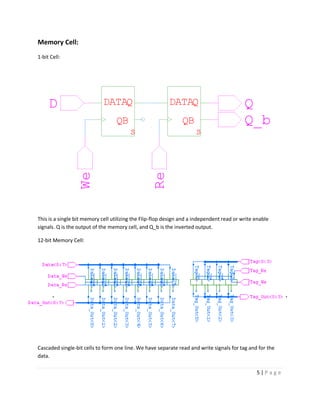
Memory Cell:
1-bit Cell:


This is a single bit memory cell utilizing the Flip-flop design and a independent read or write enable
signals. Q is the output of the memory cell, and Q_b is the inverted output.

12-bit Memory Cell:


Cascaded single-bit cells to form one line. We have separate read and write signals for tag and for the
data.

                                                                                                5|P a ge
Read/Write Test:


                   6|P a ge
1-bit Demux 1-to-4


1-bit Mux 4-to-1


                     7|P a ge
Demux 1-to-4 Test:


                     8|P a ge
Mux 4-to-1 Test:


                   9|P a ge
4-bit Tag Comparator:


Comparator Test:


                        10 | P a g e
Core Layout:


Core + Pads + Test Signals Layout:


                                     11 | P a g e
Core Placement and Layout:


Core = 2448λ x 1232.5λ

SPR Setup:

3-metal Layers:
H2: Metal3
V-H2: Via2
V: Metal2
H1-V: Via1
H1: Metal1


                             12 | P a g e
PadFrame Placement and Layout:


Placement and Routing Summary:
SPR SUMMARY 'mAMIs050DL_AND_PADS.tdb'
Date and time : 05/22/2008-21:12
1 Lambda = 1.000 Lambda = 3.333 Micron(s)
Design file : E:reda en160 proj BUmAMIs050DL_AND_PADS.tdb
Netlist file : Projectcache_pads.tpr
Library file : mAMIs050DL_AND_PADS.tdb

Placement optimization factor : 1.00
Routing optimization (3 layer) : Netlength and via reduction

Standard Cell Place and Route done :
- Core cell "Core" generated.
- Padframe cell "Min_Frame" generated.
- Chip cell "Library_Test_s" generated.
-------------------------------------------------------------
Number of standard cells : 184
Number of signals in netlist : 336

Core size in Lambda : 2438.5 x 1128.5
Core area (Lambda^2) : 2751847.25

Frame size in Lambda : 5000.00 x 5000.00
Frame area (Lambda^2) : 25000000.00

Length of nets in core : 161951.00 Lambda
Generated vias in core : 647

SPR elapsed time : 0:00:04
                                                                13 | P a g e
DRC Error Check:
L-Edit DRC SUMMARY REPORT

                              EXECUTION SUMMARY
Execution Start Time                                              May 22 2008 21:20:11
L-Edit Version                                    L-Edit Win32 12.10.20060718.19:30:32
Rule Set Name        MOSIS AMI 0.50UM - SUBMICRON RULES_ Last Updated 10/08/2001
File Name                          E:reda en160 proj BUmAMIs050DL_AND_PADS.tdb
Cell Name                                              Channel_4 (May 22 21:20:08 2008)
User Name                                                                         Rotor
Computer Name                                                             SREDA-XP1
Memory used at start                                                             46.5M

 DRC JOB RESULTS SUMMARY
Total DRC Errors Generated        0
CPU Time                   00:00:05
Real Time                  00:00:05
Rules Executed                   93

                              DRC Errors Generated by Rule Set
DRC Standard Rule Set                                                                     0

                        RUN-TIME DRC ERRORS AND WARNINGS


                       GEOMETRY FLAG SUMMARY
ACUTE ANGLES                                                                      Disabled
ALL ANGLE EDGES                                                                          0
OFFGRID                                                                           Disabled
ZERO-WIDTH WIRES                                                                         0
POLYGONS WITH OVER 199 VERTICES                                                          0
WIRES WITH OVER 200 VERTICES                                                             0
SELF INTERSECTIONS                                                                       0
WIRE JOIN/END STYLES                                                                     0


                              CELLS WITH ERRORS FOUND

      RESULTS SUMMARY
DRC Errors Generated            0
CPU Time                 00:00:05
REAL Time                00:00:05
Input Objects           404 (404)
Rules Executed                 93
Geometry Flags Executed         6
Disabled Rules                 18


                                                                                              14 | P a g e
DRC Geometry Error Details (Acute Angles):


Error #1


Error #6


These error checks were disabled.

                                             15 | P a g e
Systems Analysis:
Single-bit Read/Write Systems Test:


                                      16 | P a g e
Status Hit/Miss Systems Test:


Timing Analysis:

Read time:

      tdf = 17ns

      tdr = 9ns


                                17 | P a g e
Conclusion:

We successfully implemented a Cache Memory Simulation device. All verification data appears to meet
the design criteria. There were unpredictable design errors on the way, but none that stopped the cache
memory to function normally. DRC errors turned up geometrical errors on the Padless frame generated
by SPR. The DRC errors also determined that there were some metal to metal spacing errors in the core
after SPR. There were also disconnected Metal layers on the Padless Frame that had to be manually
connected.

We have not yet expanded the design to include fetching control systems to a Main Memory system.
This is a functionality that can be added on in the future. We also have not expanded the cache size, to
determine the maximum size of cache that is possible using the type of memory cells that we have.

Other improvements would be to actually use 6T SRAM cell design for the memory cell instead of Flip-
flops that requires more area due to more transistors in each memory cell.


                                                                                             18 | P a g e
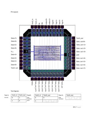
Pin Layout:


                                                                                                                            Index<0>
                                                                                                                                            Index<1>
                                                    Test2_in

                                                                  Test1_in


                                                                                                                                                            Tag<0>

                                                                                                                                                                               Tag<1>
                                                                                                                                                                                                 Tag<2>
                                                                                                                                                                                                             Tag<3>
                                                                                                 We
                                                                                  Re
           Data<7>                                                                                                                                                                                                                  Test1_out
           Data<6>                                                                                                                                                                                                                  Data_out<0>
           Data<5>                                                                                                                                                                                                                  Data_out <1>

           Data<4>                                                                                                                                                                                                                  Data_out <2>
           Vd-d                                                                                                                                                                                                                     Data_out <3>
           Data<3>                                                                                                                                                                                                                  gnd
           Data<2>                                                                                                                                                                                                                  Data_out <4>
           Data<1>                                                                                                                                                                                                                  Data_out <5>
           Data<0>                                                                                                                                                                                                                  Data_out <6>
           Test3_out                                                                                                                                                                                                                Data_out <7>
                                                Status

                                                               Data_out_sl<7>

                                                                                Data_out_sl<6>
                                                                                                 Data_out_sl<5>

                                                                                                                      Data_out_sl<4>

                                                                                                                                       Data_out_sl<3>

                                                                                                                                                        Data_out_sl<2>

                                                                                                                                                                         Data_out_sl<1>


                                                                                                                                                                                                           Test2_out
                                                                                                                                                                                          Data_out_sl<0>


           Test Signals:

Test 1:     Test1_in       Test1_out   Test2:                    Test2_in                                         Test2_out                                                                     Test 3:                Test3_out
Inverter    0              1           Ring                      0                                                0                                                                             Ring
                                       Oscillator                                                                                                                                               Oscillator
            1              0           w/En                      1


                                                                                                                                                                                                                               19 | P a g e

Cache

  • 1.
    EN160: VLSI Project Spring 2008 Cache Memory Simulation By: Holiano, Chaka, and Rotor
  • 2.
    Index Title Page no. 0.0 Tables of Contents 1 1.0 System Overview 2 1.1 -System Diagram 2 1.2 -Specifications 2 1.3 -I/O List 3 1.4 -Direct-mapped Cache Algorithm 3 1.5 -Main Components Description 4 2.0 Components Descriptions 2.1 -Memory Cell 5 2.2 -Memory Cell Tests and Timing 6 2.3 -Demux 1-to-4 7 2.4 -Mux 4-to-1 7 2.5 -Demux 1-to-4 Tests 8 2.6 -Mux 1-to-4 Tests 9 2.7 -4-bit Tag Comparator 10 2.8 -4-bit Tag Comparator Tests 10 3.0 Final System 3.0 -Core Layout 11 3.1 -Core + Pads + Test Signal Layout 11 3.2 -Core Placement and Layout 12 3.3 -SPR Setup 12 3.4 -PADFrame Placement and Layout 13 3.5 -Placement and Routing Summary 13 3.6 -DRC Error Check 14 3.7 -DRE Geometry Error Details (disabled check) 15 4.0 Systems Testing 4.1 -Read/Write Test 16 4.2 -Hit/Miss Test 17 4.3 -Hit/Miss Timing Analysis 17 5.0 Conclusion 18 6.0 Pin Layout 19 1|P a ge
  • 3.
    System Diagram: Tag_In Line_In Data_In 4bits 2bit 8bit We Tag Line Data F2 Tag Data Re Demux 4 bits Tag Data 4 bits Tag Data Tag Data Comparator Demux 4 bits F1 32 bits 4 bits Mux 2 bits 8 bits Status Data_Out Specification: Data width: 8-bit Tag: 4-bit Address: 4-bit Index 2-bit Replacement Policy: Direct Mapped Cache Fill Perform the following functions: Operation Read_en Write_en Status Data Out Read-Hit 1 X 1 Mem[index] Read-Miss 1 X 0 Previous Data Write-Hit 0 1 X X Write-Miss 0 1 X X 2|P a ge
  • 4.
    Inputs: From CPU: New Data: 8-bit Address: 6-bit Address<5:2> Tag: 4-bit Address<1:0> Index: 2-bit Read enable: 1-bit Write enable: 1-bit Outputs: To CPU: Dataout: 8-bit Status: 1-bit [Signifies when data is ready] Total pins required: 25pins + 1 Vdd + 1 gnd. Extra outputs: Ring Oscillator Test Signal: 1-bit Ring Oscillator Test Signal w/En: 2-bits Inverter: 2-bits Replacement Algorithm: Direct Mapped Cache Fill This is the fastest algorithm for cache replacement where the cache takes 2 least significant bits of the address as index. It essentially takes the main memory address and indexes the address by using modulus. 3|P a ge
  • 5.
    Main components: Muxes/Demuxes –The memory design simulates a cache memory, similar to a register memory. Muxes are essential in ensuring that data from the memory cells can be selected for the output. The demuxes is essential in ensuring that the signals between the components arrive at the correct memory cell for proper operation. Memory – Stores all the cache memory data, read or write only. In the design, read is prominent, you cannot write while read is on, but you can read while write is on. The memory cells are designed using flip-flops, and modified to have two signals for read and write enables. In each memory line/cell we store 8-bits of actual data, and 4-bit for tag comparison. Comparator – Compares the Tag of the data from the memory, and the Tag of the data requested. 4|P a ge
  • 6.
    Memory Cell: 1-bit Cell: Thisis a single bit memory cell utilizing the Flip-flop design and a independent read or write enable signals. Q is the output of the memory cell, and Q_b is the inverted output. 12-bit Memory Cell: Cascaded single-bit cells to form one line. We have separate read and write signals for tag and for the data. 5|P a ge
  • 7.
  • 8.
    1-bit Demux 1-to-4 1-bitMux 4-to-1 7|P a ge
  • 9.
  • 10.
  • 11.
  • 12.
    Core Layout: Core +Pads + Test Signals Layout: 11 | P a g e
  • 13.
    Core Placement andLayout: Core = 2448λ x 1232.5λ SPR Setup: 3-metal Layers: H2: Metal3 V-H2: Via2 V: Metal2 H1-V: Via1 H1: Metal1 12 | P a g e
  • 14.
    PadFrame Placement andLayout: Placement and Routing Summary: SPR SUMMARY 'mAMIs050DL_AND_PADS.tdb' Date and time : 05/22/2008-21:12 1 Lambda = 1.000 Lambda = 3.333 Micron(s) Design file : E:reda en160 proj BUmAMIs050DL_AND_PADS.tdb Netlist file : Projectcache_pads.tpr Library file : mAMIs050DL_AND_PADS.tdb Placement optimization factor : 1.00 Routing optimization (3 layer) : Netlength and via reduction Standard Cell Place and Route done : - Core cell "Core" generated. - Padframe cell "Min_Frame" generated. - Chip cell "Library_Test_s" generated. ------------------------------------------------------------- Number of standard cells : 184 Number of signals in netlist : 336 Core size in Lambda : 2438.5 x 1128.5 Core area (Lambda^2) : 2751847.25 Frame size in Lambda : 5000.00 x 5000.00 Frame area (Lambda^2) : 25000000.00 Length of nets in core : 161951.00 Lambda Generated vias in core : 647 SPR elapsed time : 0:00:04 13 | P a g e
  • 15.
    DRC Error Check: L-EditDRC SUMMARY REPORT EXECUTION SUMMARY Execution Start Time May 22 2008 21:20:11 L-Edit Version L-Edit Win32 12.10.20060718.19:30:32 Rule Set Name MOSIS AMI 0.50UM - SUBMICRON RULES_ Last Updated 10/08/2001 File Name E:reda en160 proj BUmAMIs050DL_AND_PADS.tdb Cell Name Channel_4 (May 22 21:20:08 2008) User Name Rotor Computer Name SREDA-XP1 Memory used at start 46.5M DRC JOB RESULTS SUMMARY Total DRC Errors Generated 0 CPU Time 00:00:05 Real Time 00:00:05 Rules Executed 93 DRC Errors Generated by Rule Set DRC Standard Rule Set 0 RUN-TIME DRC ERRORS AND WARNINGS GEOMETRY FLAG SUMMARY ACUTE ANGLES Disabled ALL ANGLE EDGES 0 OFFGRID Disabled ZERO-WIDTH WIRES 0 POLYGONS WITH OVER 199 VERTICES 0 WIRES WITH OVER 200 VERTICES 0 SELF INTERSECTIONS 0 WIRE JOIN/END STYLES 0 CELLS WITH ERRORS FOUND RESULTS SUMMARY DRC Errors Generated 0 CPU Time 00:00:05 REAL Time 00:00:05 Input Objects 404 (404) Rules Executed 93 Geometry Flags Executed 6 Disabled Rules 18 14 | P a g e
  • 16.
    DRC Geometry ErrorDetails (Acute Angles): Error #1 Error #6 These error checks were disabled. 15 | P a g e
  • 17.
    Systems Analysis: Single-bit Read/WriteSystems Test: 16 | P a g e
  • 18.
    Status Hit/Miss SystemsTest: Timing Analysis: Read time:  tdf = 17ns  tdr = 9ns 17 | P a g e
  • 19.
    Conclusion: We successfully implementeda Cache Memory Simulation device. All verification data appears to meet the design criteria. There were unpredictable design errors on the way, but none that stopped the cache memory to function normally. DRC errors turned up geometrical errors on the Padless frame generated by SPR. The DRC errors also determined that there were some metal to metal spacing errors in the core after SPR. There were also disconnected Metal layers on the Padless Frame that had to be manually connected. We have not yet expanded the design to include fetching control systems to a Main Memory system. This is a functionality that can be added on in the future. We also have not expanded the cache size, to determine the maximum size of cache that is possible using the type of memory cells that we have. Other improvements would be to actually use 6T SRAM cell design for the memory cell instead of Flip- flops that requires more area due to more transistors in each memory cell. 18 | P a g e
  • 20.
    Pin Layout: Index<0> Index<1> Test2_in Test1_in Tag<0> Tag<1> Tag<2> Tag<3> We Re Data<7> Test1_out Data<6> Data_out<0> Data<5> Data_out <1> Data<4> Data_out <2> Vd-d Data_out <3> Data<3> gnd Data<2> Data_out <4> Data<1> Data_out <5> Data<0> Data_out <6> Test3_out Data_out <7> Status Data_out_sl<7> Data_out_sl<6> Data_out_sl<5> Data_out_sl<4> Data_out_sl<3> Data_out_sl<2> Data_out_sl<1> Test2_out Data_out_sl<0> Test Signals: Test 1: Test1_in Test1_out Test2: Test2_in Test2_out Test 3: Test3_out Inverter 0 1 Ring 0 0 Ring Oscillator Oscillator 1 0 w/En 1 19 | P a g e