Principles of CommunicationSystems
BEC403 - IPCC
(4th Sem – ECE)
Prof. Prakasha G
Dept. Of ECE
Sri Venkateshwara College of Engineering (SVCE)
Bengaluru – 562 157
2.
SVCE - Vision& Mission
Our Vision
To be a premier institute for addressing the challenges in global perspective.
Our Mission
M1: Nurture students with professional and ethical outlook to identify
needs, analyze, design and innovate sustainable solutions through lifelong
learning in service of society as individual or a team.
M2: Establish state-of-the-art Laboratories and Information Resource centre
for education and research.
M3: Collaborate with Industry, Government Organization and Society to align
the curriculum and outreach activities.
3.
ECE Department Vision& Mission
Vision
To be a centre of excellence in Electronics, Communication and allied domains
for Education and Research.
Mission
M1: Nurture students with strong technical foundation through effective
teaching-learning processes and state-of-the-art infrastructure.
M2: Inculcate ethical values, leadership qualities, lifelong learning, individual
and teamwork abilities amongst the students through holistic education.
M3: Collaborate with industry and society to provide eco-friendly & sustainable
solutions.
4.
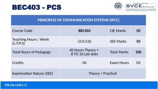
BEC403 - PCS
PRINCIPLESOF COMMUNICATION SYSTEMS (IPCC)
Course Code BEC403 CIE Marks 50
Teaching Hours / Week
(L:T:P:S) (3:0:2:0) SEE Marks 50
Total Hours of Pedagogy 40 Hours Theory +
8 TO 10 Lab slots Total Marks 100
Credits 04 Exam Hours 03
Examination Nature (SEE) Theory / Practical
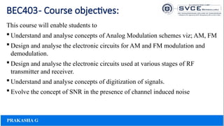
BEC403- Course objectives:
Thiscourse will enable students to
Understand and analyse concepts of Analog Modulation schemes viz; AM, FM
Design and analyse the electronic circuits for AM and FM modulation and
demodulation.
Design and analyse the electronic circuits used at various stages of RF
transmitter and receiver.
Understand and analyse concepts of digitization of signals.
Evolve the concept of SNR in the presence of channel induced noise
7.
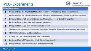
IPCC- Experiments
Sl. NoExperiments
1 Design and Test the Amplitude Modulation and demodulation using diode and transistors.
2 Design and Test the Frequency modulation using VCO and demodulation using slope detector circuit.
3 Design and test a high power a) Class A line RF amplifier. b) Class E RF amplifier
4 Design and test a mixer used for frequency translation.
5 Design and test a VCO used for local oscillator service
6 Verification of Sampling Theorem using sampling a sinusoidal signal using a sample and hold circuit.
7 TDM PAM Multiplexer and Demultiplexer
8 A String DAC and Flash Converter (Demo Experiment)
9 Design and Test a RF Transmitter circuit (Demo Experiment)
10 Design and Test a RF Receiver circuit (Demo Experiment)
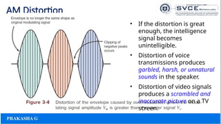
AM Distortion
• Ifthe distortion is great
enough, the intelligence
signal becomes
unintelligible.
• Distortion of voice
transmissions produces
garbled, harsh, or unnatural
sounds in the speaker.
• Distortion of video signals
produces a scrambled and
inaccurate picture on a TV
screen.
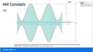
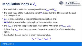
Modulation Index =Vm
• The modulation index can be computed from Vmax and Vmin
• The peak value of the modulating signal Vm is one-half the difference of the peak
and trough values.
• Vmax is the peak value of the signal during modulation, and
• Vmin is the lowest value, or trough, of the modulated wave.
• The Vmax is one-half the peak-to-peak value of the AM signal, or Vmax (p - p)/2.
• Subtracting Vmin from Vmax produces the peak to peak value of the modulating
signal.
• One-half of that, of course, is simply the peak value.
Vm = (Vmax – Vmin) / 2
12.
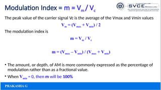
Modulation Index =m = Vm / Vc
The peak value of the carrier signal Vc is the average of the Vmax and Vmin values
Vm = (Vmax + Vmin) / 2
The modulation index is
m = Vm / Vc
m = (Vmax – Vmin) / (Vmax + Vmin)
• The amount, or depth, of AM is more commonly expressed as the percentage of
modulation rather than as a fractional value.
• When Vmin = 0, then m will be 100%
13.
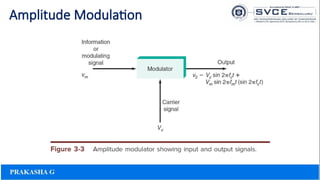
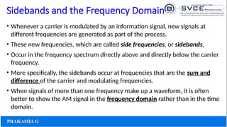
Sidebands and theFrequency Domain
• Whenever a carrier is modulated by an information signal, new signals at
different frequencies are generated as part of the process.
• These new frequencies, which are called side frequencies, or sidebands,
• Occur in the frequency spectrum directly above and directly below the carrier
frequency.
• More specifically, the sidebands occur at frequencies that are the sum and
difference of the carrier and modulating frequencies.
• When signals of more than one frequency make up a waveform, it is often
better to show the AM signal in the frequency domain rather than in the time
domain.
14.
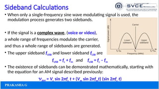
Sideband Calculations
• Whenonly a single-frequency sine wave modulating signal is used, the
modulation process generates two sidebands.
• If the signal is a complex wave, (voice or video),
a whole range of frequencies modulate the carrier,
and thus a whole range of sidebands are generated.
• The upper sideband fUSB and lower sideband fLSB are
fUSB = fc + fm and fLSB = fc – fm
• The existence of sidebands can be demonstrated mathematically, starting with
the equation for an AM signal described previously:
vAM = Vc sin 2πfc t + (Vm sin 2πfmt) (sin 2πfc t)
15.
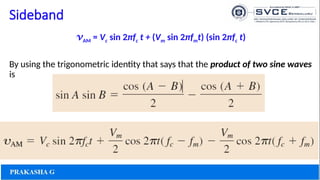
Sideband
vAM = Vcsin 2πfc t + (Vm sin 2πfmt) (sin 2πfc t)
By using the trigonometric identity that says that the product of two sine waves
is
16.
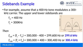
Sidebands Example
•For example,assume that a 400-Hz tone modulates a 300-
kHz carrier. The upper and lower sidebands are
fm = 400 Hz
fc = 300KHz
Then
fLSB = (fc – fm) = 300,000 - 400 = 299,600 Hz or 299.6 kHz
fUSB = (fc + fm)= 300,000 + 400 = 300,400 Hz or 300.4 kHz
17.
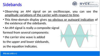
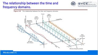
Sidebands
• Observing anAM signal on an oscilloscope, you can see the
amplitude variations of the carrier with respect to time.
• This time-domain display gives no obvious or outward indication of
the existence of the sidebands.
• An AM signal is really a composite signal
formed from several components:
• the carrier sine wave is added
to the upper and lower sidebands,
as the equation indicates.
18.
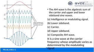
• The AMwave is the algebraic sum of
the carrier and upper and lower
sideband sine waves.
(a) Intelligence or modulating signal.
(b) Lower sideband.
(c) Carrier.
(d) Upper sideband.
(e) Composite AM wave.
It is a sine wave at the carrier
frequency whose amplitude varies as
determined by the modulating
signal.
19.
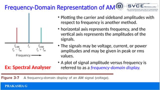
Frequency-Domain Representation ofAM
• Plotting the carrier and sideband amplitudes with
respect to frequency is another method.
• horizontal axis represents frequency, and the
vertical axis represents the amplitudes of the
signals.
• The signals may be voltage, current, or power
amplitudes and may be given in peak or rms
values.
• A plot of signal amplitude versus frequency is
referred to as a frequency-domain display.
Ex: Spectral Analyser
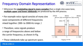
Frequency Domain Representation
•Whenever the modulating signal is more complex than a single sine wave tone,
multiple upper and lower sidebands are produced by the AM process.
• For example voice signal consists of many sine
wave components of different frequencies
mixed together. (300- to 3000-Hz range. )
• Therefore, voice signals produce
a range of frequencies above and below
the carrier frequency, as shown in Fig.
• These sidebands take up spectrum space.
22.
• The totalbandwidth of an AM signal is calculated by computing the maximum
and minimum sideband frequencies.
• This is done by finding the sum and difference of the carrier frequency and
maximum modulating frequency (3000 Hz, or 3 kHz, in Fig).
• For example, if the carrier frequency is 2.8 MHz (2800 kHz), then the
maximum and minimum sideband frequencies are
fUSB = 2800 + 3 = 2803 kHz and fLSB + 2800 - 3 = 2797 kHz


![[DSC Europe 25] Josip Saban - Career building for data professionals.pptx](https://cdn.slidesharecdn.com/ss_thumbnails/zroflcttkm1vmli0txea-josip-saban-career-building-for-data-professionals-260123083019-587cdb8c-thumbnail.jpg?width=640&height=640&fit=bounds)


