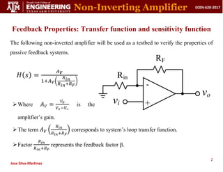
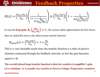
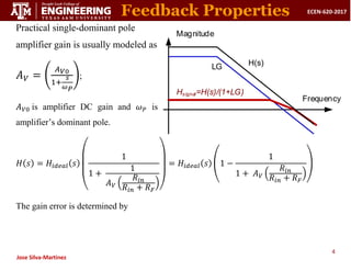
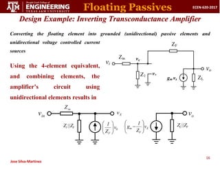
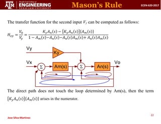
SlideShare a Scribd company logo
1 of 39
Download to read offline
1
ECEN-620-2017
Jose Silva-Martinez
Basic Concepts: Amplifiers and Feedback
Jose Silva-Martinez
Department of Electrical & Computer Engineering
Texas A&M University
2
ECEN-620-2017
Jose Silva-Martinez
Feedback Properties: Transfer function and sensitivity function
The following non-inverted amplifier will be used as a testbed to verify the properties of
passive feedback systems.
𝐻(𝑠) =
𝐴𝑉
1+𝐴𝑉(
𝑅𝑖𝑛
𝑅𝑖𝑛+𝑅𝐹
)
Where 𝐴𝑉 =
𝑉0
𝑉+−𝑉−
is the
amplifier’s gain.
The term 𝐴𝑉 (
𝑅𝑖𝑛
𝑅𝑖𝑛+𝑅𝐹
) corresponds to system’s loop transfer function.
Factor
𝑅𝑖𝑛
𝑅𝑖𝑛+𝑅𝐹
represents the feedback factor .
vi
+
-
vo
RF
Rin
Non-Inverting Amplifier
3
ECEN-620-2017
Jose Silva-Martinez
𝐻(𝑠) = (
𝑅𝑖𝑛+𝑅𝐹
𝑅𝑖𝑛
) (
1
1+
1
𝐴𝑉(
𝑅𝑖𝑛
𝑅𝑖𝑛+𝑅𝐹
)
) ≅ (
𝑅𝑖𝑛+𝑅𝐹
𝑅𝑖𝑛
) (1 −
1
𝐴𝑉(
𝑅𝑖𝑛
𝑅𝑖𝑛+𝑅𝐹
)
)
In case the loop gain 𝑨𝑽 (
𝑹𝒊𝒏
𝑹𝒊𝒏+𝑹𝑭
) ≫ 𝟏 , the system safely approximates the first factor,
then we called this term as the ideal system transfer function
𝐻𝑖𝑑𝑒𝑎𝑙(𝑠) = (
𝑅𝑖𝑛+𝑅𝐹
𝑅𝑖𝑛
) = 1 +
𝑅𝐹
𝑅𝑖𝑛
This is a very desirable result since the transfer function is a ratio of passive
elements connected through the feedback network; in fact the gain becomes
equal to 1/.
The overall (closed loop) transfer function is then low sensitive to amplifier’s gain
(AV) variations. AV is usually very sensitive to Process-Voltage-Temperature variations
Feedback Properties
4
ECEN-620-2017
Jose Silva-Martinez
Practical single-dominant pole
amplifier gain is usually modeled as
𝐴𝑉 = (
𝐴𝑉0
1+
𝑠
𝜔𝑃
);
𝐴𝑉0 is amplifier DC gain and 𝜔𝑃 is
amplifier’s dominant pole.
𝐻(𝑠) = 𝐻𝑖𝑑𝑒𝑎𝑙(𝑠)
(
1
1 +
1
𝐴𝑉 (
𝑅𝑖𝑛
𝑅𝑖𝑛 + 𝑅𝐹
)
)
= 𝐻𝑖𝑑𝑒𝑎𝑙(𝑠) (1 −
1
1 + 𝐴𝑉 (
𝑅𝑖𝑛
𝑅𝑖𝑛 + 𝑅𝐹
)
)
The gain error is determined by
Feedback Properties
LG
Hsignal=H(s)/(1+LG)
Magnitude
Frequency
H(s)
5
ECEN-620-2017
Jose Silva-Martinez







 



















in
F
in
V
P
R
R
R
A
s
Gain
Loop
Gain
Loop
s
0
1
1
1
1
)
(


.
It is important to recognize that the error function is equal to 1/(loop gain).
Error function monotonically increases after the first pole of loop gain.
High frequency signals do not benefit from feedback as much as in-band (low
frequency) signals
Error Function
6
ECEN-620-2017
Jose Silva-Martinez







 














in
F
in
0
V
P
R
R
R
A
s
1
)
s
(


.
 The error function is inversely proportional to amplifier’s frequency
response.
f (Hz)
20 log10(|AV(s)|)
-20 dB/decade

106 dB
unity-gain
frequency
0 dB
20 dB/decade
Error (dB)
7
ECEN-620-2017
Jose Silva-Martinez
To maintain good accuracy, loop gain must be high enough until the
maximum frequency of interest.
For a closed loop system with a
targeted error 0, we must satisfy the
following condition:
0
in
F
in
0
V
2
P
max
R
R
R
A
f
f
1
)
s
( 
 







 


























max is the maximum frequency of interest, often defined as system
bandwidth.
f (Hz)

0 dB
unity-gain
frequency
20 dB/decade
Error (dB)
-100 dB

fmax
fP
Error Function
8
ECEN-620-2017
Jose Silva-Martinez
For the case max /P >10, the condition for limited
overall gain error can be simplified to
0
in
F
in
0
V
P
max
R
R
R
A
f
f
)
s
( 
 







 













.
If AV0 = 105
V/V (considered very large for CMOS
solutions), the error measured at different frequencies
is listed in this Table.
1+RF/Rin ωmax/ ωP
Error
magnitude
10 0.01 ~ 10-4
10 1 ~1.4∙10-4
10 10 ~10-3
10 100 ~10-2
10 1000 ~10-1
100 10 ~10-2
1000 10 ~10-1
10000 10 ~100
Error Function
9
ECEN-620-2017
Jose Silva-Martinez
Inverting Amplifier. The case of the inverting amplifier is a bit more complex than the
case of the non-inverting amplifier. Assume that the amplifier’s gain includes the effect of
the feedback network.
The voltage at the amplifier’s inverting
terminal (ERROR VOLTAGE) is:
𝑉
− = (
𝑅𝐹
𝑅𝑖𝑛+𝑅𝐹
) 𝑉𝑖 + (
𝑅𝑖𝑛
𝑅𝑖𝑛+𝑅𝐹
) 𝑉0
Output voltage
𝑉0 = −𝐴𝑉𝑉
− = −𝐴𝑉 (
𝑅𝐹
𝑅𝑖𝑛+𝑅𝐹
) 𝑉𝑖 − 𝐴𝑉 (
𝑅𝑖𝑛
𝑅𝑖𝑛+𝑅𝐹
) 𝑉0
The first term of the right most term is the so-called direct path gain
The second right hand most term is obtained in this case by breaking the loop and
grounding Vi terminal.
+
-
vo
RF
Rin
vi
Inverting Amplifiers
10
ECEN-620-2017
Jose Silva-Martinez

It can be found that signal transfer function
is determined as
𝑽𝟎
𝑽𝒊
= − (
𝑹𝑭
𝑹𝒊𝒏
) (
𝟏
𝟏+
𝟏
𝑨𝑽(
𝑹𝒊𝒏
𝑹𝒊𝒏+𝑹𝑭
)
)
Error factor is the same for both
inverting and non-inverting
configurations
+
-
vo
RF
Rin
vi
f (Hz)
20 log10(|AV(s)|)
-20 dB/decade

106 dB
unity-gain
frequency
0 dB
20 dB/decade
Error (dB)
Inverting Amplifiers
11
ECEN-620-2017
Jose Silva-Martinez
The ERROR VOLTAGE (inverting
terminal of the amplifier) is determined by
𝑉
− = (
𝑅𝐹
𝑅𝑖𝑛+𝑅𝐹
) 𝑉𝑖 + (
𝑅𝑖𝑛
𝑅𝑖𝑛+𝑅𝐹
) 𝑉0
If the amplifier gain is given by AV
and it is not affected by RF, then the error
voltage is computed as
𝑉
− =
(
𝑅𝐹
𝑅𝑖𝑛+𝑅𝐹
)
1+(𝐴𝑉)(
𝑅𝑖𝑛
𝑅𝑖𝑛+𝑅𝐹
)
𝑉𝑖 ≅ (
𝑅𝐹
𝑅𝑖𝑛
𝐴𝑉
) 𝑉𝑖
The larger the loop gain, the smaller the value of the error voltage is.
+
-
vo
RF
Rin
vi
Inverting Amplifier
LG
Herror=1/(1+LG)
Magnitude
Frequency
12
ECEN-620-2017
Jose Silva-Martinez
Let us go a bit deeper: Systematic and Intuitive Analysis
Transconductance amplifiers with floating elements in feedback Network
Typically the CMOS amplifier does not have a low-impedance output stage: these
are the most practical cases since buffers
present voltage headroom issues.
The analysis of this type of amplifiers is
cumbersome, and often we get lost on
the algebra.
The results of typical analysis are not
evident and hard to be properly interpreted; results are not intuitive!
We would like to get insights and so guidelines to optimize our architecture and design
procedures.
vi
vo
Zin
Zi
ZF
ZL
+
-
Transconductance Amplifiers
13
ECEN-620-2017
Jose Silva-Martinez
Let us first consider the case of the inverting amplifier including amplifier’s input and
output impedance.
 The transimpedance amplifier’s small signal model employing a voltage controlled
current source is used here.
Using KCL at both nodes vx
and vo we find
𝑉𝑋 (
1
𝑍𝑖𝑛
+
1
𝑍1
+
1
𝑍𝐹
) −
𝑉0
𝑍𝐹
=
𝑉𝑖
𝑍𝑖𝑛
𝑉𝑋 (𝑔𝑚 −
1
𝑍𝐹
) + 𝑉0 (
1
𝑍𝐿
+
1
𝑍𝐹
) = 0
Solving these equations result in
𝑉0
𝑉𝑖
= −
𝑌𝑖𝑛
𝑌𝐹(1+(
𝑌𝑖𝑛+𝑌1+𝑌𝐹
𝑌𝐹
)(
𝑌𝐿+𝑌𝐹
𝑔𝑚−𝑌𝐹
))
Notice that loop gain is then given by 𝐿𝐺 = (
𝑌𝐹
𝑌𝑖𝑛+𝑌1+𝑌𝐹
) (
𝑔𝑚− 𝑌𝐹
𝑌𝐿+𝑌𝐹
)
vi
vo
Zin
Z1
ZF
vx
i1 ii
io
ZL
gm vx
v+
Transconductance Amplifiers
14
ECEN-620-2017
Jose Silva-Martinez
𝐿𝐺 = (
𝑍𝑖𝑛 ∥ 𝑍1
𝑍𝑖𝑛 ∥ 𝑍1 + 𝑍𝐹
) [(𝑔𝑚 −
1
𝑍𝐹
) (𝑍𝐿 ∥ 𝑍𝐹)]
The first term is the feedback factor,
The 2nd factor is the amplifier’s gain.
Notice that amplifier’s transconductance gain is affected by the feedback element!
A right hand plane zero arises when ZF is capacitive; that may hurt your phase margin.
When considering capacitors
or more complex networks it
is not evident where the poles
and zeros are located.
The culprit for these
complications is the floating
element ZF.
vi
vo
Zin
Z1
ZF
vx
ZL
gm vx
v+
Transconductance Amplifiers
15
ECEN-620-2017
Jose Silva-Martinez
Modeling Bi-Directional Floating Impedances
A major issue is the mapping of circuits that have bi-directional elements connecting
different nodes.
The representation of the floating element ZF through the four components
depicted above is consistent and accurate.
The 4-element representation uses unidirectional (without floating passives)
Resulting passive components are grounded (unidirectional)
This model can be easily incorporated into the block diagram’s representation and then
solved by using Mason’s rule.
va vb
iab
Zab Zab
vb
iab
Zab
Zab
va
va vb
iab
Zab
Floating Passives
16
ECEN-620-2017
Jose Silva-Martinez
Design Example: Inverting Transconductance Amplifier
Converting the floating element into grounded (unidirectional) passive elements and
unidirectional voltage controlled current
sources
Using the 4-element equivalent,
and combining elements, the
amplifier’s circuit using
unidirectional elements results in
vi
vo
Zin
Z1
ZF
vx
ZL
gm vx
v+
X
F
m v
Z
1
g 







 F
L Z
||
Z
0
F
v
Z
1








F
1 Z
||
Z
in
v o
v
in
Z
X
v
Floating Passives
17
ECEN-620-2017
Jose Silva-Martinez
Feedforward gain and loop Gain can be easily found as
𝐹𝐹 = (
𝑍1||𝑍𝐹
𝑍𝑖𝑛+𝑍1||𝑍𝐹
) ((𝑔𝑚 −
1
𝑍𝐹
) 𝑍𝐿||𝑍𝐹) ;
𝐿𝐺 = (
𝑍𝑖𝑛||𝑍1||𝑍𝐹
𝑍𝐹
) ((𝑔𝑚 −
1
𝑍𝐹
) 𝑍𝐿||𝑍𝐹)
The effect of the feedback impedance on the amplifier’s transconductance is
evident in this model.
Exact location of poles and zeros are now captured, and exact computation of
both loop gain and closed loop transfer function is straightforward.
X
F
m v
Z
1
g 







 F
L Z
||
Z
0
F
v
Z
1








F
1 Z
||
Z
in
v o
v
in
Z
X
v
Floating Passives
18
ECEN-620-2017
Jose Silva-Martinez
Unidirectional Block Diagrams and Mason Rule
An elegant yet more insightful solution for unidirectional networks employs the
Mason rule.
 Unidirectional building blocks means that the output is driven by the input, but
variations at the output does not affect at all the block’s input.
 Examples of these blocks are
a)Voltage controlled voltage sources, voltage controlled current sources,
current controlled voltage sources and current controlled current sources.
b)Grounded passives (resistors, capacitors and inductors)
c)Examples of non-directional elements are the transformers, and floating
impedances
 The transfer function of a given linear system represented by “unidirectional
building blocks” can always be obtained by identifying loops and direct
trajectories.
Mason’s Rule
19
ECEN-620-2017
Jose Silva-Martinez
Once the system is represented by unidirectional elements, we must:
 Identify the direct trajectories(paths) from the input(s) to output
KyAn(s) from Vy to output
AmAn from Vx to output
 The loops must also be
identified
Am(s)
 Loops that are not touched by certain direct paths; e.g.
The loop is not touched by the direct path KyAn
 The loops that are not sharing elements or nodes (un-touched loops) have to be
identified. In this case we do not find any of these loops.
Feedback Properties
S An(s)
S
Am(s)
Ky
Vy
Vx Vo
20
ECEN-620-2017
Jose Silva-Martinez
For the schematic, the following paths and loop can be identified:
i) Direct path 1 from Vy: KyAnVy
ii) Direct path 2 from Vx:
Am(s) An(s)Vx
iii) Loop1: Am(s)
iv) Loop2: An(s)
v) Loop3: Am(s)An(s)
vi) Notice that Am(s) and An(s) do not have any element in common. This is an
example of un-touched loops
MASON Rule: If the system is linear, then every single input generates an output
component that can be computed according to the following rule:
 
 






.....
loops
untouched
of
product
loops
1
....
.....
loops
untouched
and
paths
direct
of
product
paths
direct
vi
vo
Mason’s Rule
S An(s)
S
Am(s)
Ky
Vy
Vx Vo
21
ECEN-620-2017
Jose Silva-Martinez
In the case of the following block diagram composed by unidirectional blocks we can obtain the
following transfer functions:
𝐻𝑜𝑥 =
𝑉0
𝑉𝑥
=
𝐴𝑚(𝑠)𝐴𝑛(𝑠)
1−𝐴𝑚(𝑠)
𝐻𝑜𝑦 =
𝑉0
𝑉𝑦
=
𝐾𝑦𝐴𝑛(𝑠)−{𝐾𝑦𝐴𝑛(𝑠)}{𝐴𝑚(𝑠)}
1−𝐴𝑚(𝑠)
Once all transfer functions are identified, the overall output voltage is computed as follows:
𝑉0 = 𝐻𝑜𝑦𝑉
𝑦 + 𝐻𝑜𝑥𝑉
𝑥
For the case of the second schematic, the transfer
functions can be computed as
𝐻𝑜𝑥 =
𝐴𝑚(𝑠)𝐴𝑛(𝑠)
1−𝐴𝑚(𝑠)−𝐴𝑛(𝑠)−𝐴𝑛(𝑠)𝐴𝑚(𝑠)−𝐴𝑛(𝑠)𝐴𝑚(𝑠)
The denominator is the result of the single loop
Am(s), the single loop An(s), the loop involving Am(s)An(s) and last term is due to the
product of the two non-touching loops An(s)Am(s).
Am(s) An(s)
+ +
Vx
Vy Ky
loop is not touched
by Vy path
Am(s) An(s)
+ +
Vx
Vy Ky
Untouched loops
Mason’s Rule
S An(s)
S
Am(s)
Ky
Vy
Vx Vo
22
ECEN-620-2017
Jose Silva-Martinez
The transfer function for the second input Vy can be computed as follows:
𝐻𝑜𝑦 =
𝑉0
𝑉
𝑦
=
𝐾𝑦𝐴𝑛(𝑠) − {𝐾𝑦𝐴𝑛(𝑠)}{𝐴𝑚(𝑠)}
1 − 𝐴𝑚(𝑠)−𝐴𝑛(𝑠)−𝐴𝑛(𝑠)𝐴𝑚(𝑠)+ 𝐴𝑛(𝑠)𝐴𝑚(𝑠)
The direct path does not touch the loop determined by Am(s), then the term
{𝐾𝑦𝐴𝑛(𝑠)}{𝐴𝑚(𝑠)} arises in the numerator.
Mason’s Rule
S An(s)
S
Am(s)
Ky
Vy
Vx Vo
23
ECEN-620-2017
Jose Silva-Martinez
MASON Rule: If the system is linear, then every single input generates an output
component that can be computed according to the following rule:
 
 






.....
loops
untouched
of
product
loops
1
....
.....
loops
untouched
and
paths
direct
of
product
paths
direct
vi
vo
 Zeros (numerator) are fully determined by direct paths in absence of untouched
loops.
 Direct paths that do not touch loops create additional terms and play relevant role
on the definition of the zeros
 Poles are entirely determined by the loops
 Noise shaping and sensitivity functions are quite related to the direct paths
 System quality and stability are quite related to loop transfer function
Relevant remarks from Mason’s Rule
24
ECEN-620-2017
Jose Silva-Martinez
 See some examples related to Sigma-Delta Modulators
25
ECEN-620-2017
Jose Silva-Martinez
Sensitivity Function
When dealing with multivariable functions and when some of the parameters may have
significant variations then it is useful to compute the sensitivity functions to quantify
the individual variability effects on system performance.
The sensitivity of a multivariable function H(x, y, z, …) as function of the parameter
x is defined as
 ∫
𝐻
𝑥
= (
𝑥
𝐻
) (
𝑑𝐻
𝑑𝑥
) =
(
𝑑𝐻
𝑑𝑥
)
𝐻
𝑥
or
𝑑𝐻
𝐻
= ∫ (
𝑑𝑋
𝑋
)
𝐻
𝑥
The sensitivity function represents the first order variation of H as function of
the parameter x, normalized by the factor H/x.
Properties of Sensitivity Function
26
ECEN-620-2017
Jose Silva-Martinez
To get more insight, let us consider the following approximation:
∫
𝑯
𝒙
=
𝒅𝑯
𝑯
𝒅𝒙
𝒙
≅
∆𝑯
𝑯
∆𝒙
𝒙
The sensitivity function then measures the variation of the normalized transfer
function
∆𝐻
𝐻
(percentage) as function of the variation of normalized parameter
∆𝑥
𝑥
(percentage).
If the sensitivity function is computed as 10, then 1% variation in parameter x will
produce a variation of 10% in the overall transfer function H.
Then, it is highly desirable to maintaining the sensitivity function of H with respect to
critical parameters lesser than 1.
For the case of large parameter variations such as gain and bandwidth of the
operational amplifier, it is highly desirable to keep the sensitivity functions well below
unity.
Properties of Sensitivity Function
27
ECEN-620-2017
Jose Silva-Martinez
Be careful with circuit enhancing devices such as the ones that make use of
negative resistors (positive feedback) to boost amplifier’s gain! Example:
Typical DC Amplifier’s gain: 𝐴𝑉𝑇 =
𝑔𝑚
𝐺𝐿
Enhanced voltage gain: 𝐴𝑉𝐸 =
𝑔𝑚
𝐺𝐿−𝑮𝑪
= 𝐴𝑉𝑇 (
𝟏
𝟏−
𝑮𝑪
𝑮𝑳
) = 𝐴𝑉𝑇 (
1
1− 𝑋
)
Enhancing gain factor =
1
1−
𝐺𝐶
𝐺𝐿
; for more gain boosting, GC  GL
Sensitivity function: ∫
𝑨𝑽𝑬
𝑿
= −
𝑿
𝟏− 𝑿
= −
𝑮𝑪
𝑮𝑳
𝟏−
𝑮𝑪
𝑮𝑳
=
𝟏
𝟏−
𝑮𝑳
𝑮𝑪
The design trade-off is evident! The larger the gain boosting is, the larger the amplifier
sensitivity to GC, GL tolerances is. Sweet Spots result, in most of the cases, in
very sensitive systems! Corner and Montecarlo simulations are
mandatory in these cases.
Properties of Sensitivity Function
28
ECEN-620-2017
Jose Silva-Martinez
Similar results are obtained when cancelling signal components!
Typical blocker canceling circuit: 𝐴𝑉𝑇 = 𝑔𝑚(𝑍1 − 𝑍2) = 𝑔𝑚𝑍1 (1 −
𝑍2
𝑍1
)
Z1 and Z2 are usually function of frequency; for noise or signal canceling at certain
frequency it is desirable to design the system such that Z1(c)= Z2(c) and Z1() Z2()
when c
: 𝐴𝑉𝑇 = 0 𝑤ℎ𝑒𝑛 𝜔 = 𝜔𝑐
Sensitivity function: ∫
𝟏−𝑿
𝑿
= −
𝑿
𝟏− 𝑿
= −
𝒁𝟐
𝒁𝟏
𝟏−
𝒁𝟐
𝒁𝟏
=
𝟏
𝟏−
𝒁𝟏
𝒁𝟐
The signal cancelling system is very sensitive to variations on either one of the two
impedances (or components) involved in the cancellation.
If you use partial positive feedback, be sure that you are not very aggressive in your
design; e.g.
𝒁𝟐
𝒁𝟏
(= 0.8 at 𝝎 = 𝝎𝒄)
𝒈𝒎𝒁𝟏 (𝟏 −
𝒁𝟐
𝒁𝟏
) = 𝒈𝒎𝒁𝟏(𝟎. 𝟐) 𝒘𝒉𝒊𝒍𝒆 ∫
𝒈𝒎𝒁𝟏(𝟏−
𝒁𝟐
𝒁𝟏
)
𝒁𝟐
𝒁𝟏
= 𝟓
Sensitivity Function
29
ECEN-620-2017
Jose Silva-Martinez
These results mean:
Signal attenuation by a factor of 5 (14dB) at the critical frequency, no bad
at all
If Z2/Z1 presents tolerances of 5%, then the attenuation factor will change
by 25%; worst case attenuation will be more than -11dB.
What about circuits like this: ∫
𝟏+𝑿
𝑿
?
∫
𝟏+𝑿
𝑿
= +
𝑿
𝟏 + 𝑿
The sensitivity function is <1 if and only if X > 0.
Some systems like Doherty RF Power Amplifiers make use of this
property
30
ECEN-620-2017
Jose Silva-Martinez
Non-Inverting Amplifier. Let us consider the case of the non-inverting amplifier:
𝐻(𝑠) = (
𝑅𝑖𝑛+𝑅𝐹
𝑅𝑖𝑛
) (
1
1+
1
𝐴𝑉(
𝑅𝑖𝑛
𝑅𝑖𝑛+𝑅𝐹
)
) = (
𝑅𝑖𝑛+𝑅𝐹
𝑅𝑖𝑛
) (
1
1+𝜉
)
The computation of the sensitivity of H with respect to the error function 𝜉LGyields,
∫
𝐻
𝜉
= (
𝜉
(
𝑅𝑖𝑛+𝑅𝐹
𝑅𝑖𝑛
)(
1
1+𝜉
)
) (
𝑑
𝑑𝜉
(
𝑅𝑖𝑛+𝑅𝐹
𝑅𝑖𝑛
) (
1
1+𝜉
)) = −
𝜉
1+𝜉
 In case 𝜉 ≪ 1, the sensitivity function can be approximated as ∫
𝐻
𝜉
≅ −𝜉
 The error function is computed as 𝜉 =
1
𝐿𝑜𝑜𝑝 𝐺𝑎𝑖𝑛
=
1
𝐴𝑉(
𝑅𝑖𝑛
𝑅𝑖𝑛+𝑅𝐹
)
 If, we expect variations of 𝜉 in the range of 100% but we do want the effects on H(s) to be more
than 1%, then 𝜉 must be maintained under 0.01; e.g. overall loop gain > 40dB.
Main Concepts behind Feedback
31
ECEN-620-2017
Jose Silva-Martinez
Better Linearity: Intuitively, when loop gain is large, the error function
decreases, thus better linearity figures are obtained; error voltage is the
input of your OPAMP. Assumption: the feedback network is linear!
The ERROR VOLTAGE is determined by
𝑽− =
(
𝑹𝑭
𝑹𝒊𝒏 + 𝑹𝑭
)
𝟏 + (𝑨𝑽) (
𝑹𝒊𝒏
𝑹𝒊𝒏 + 𝑹𝑭
)
𝑽𝒊
≅ (
𝑹𝑭
𝑹𝒊𝒏
𝑨𝑽
) 𝑽𝒊
 If loop gain is large, then amplifier’s (true) input signal swing reduces at the same time!
 Non-linearities due to AV are drastically attenuated (small signal operation mode)
+
-
vo
RF
Rin
vi
Properties of Feedback: Linearity
32
ECEN-620-2017
Jose Silva-Martinez
General Remarks:
 Entire loop transfer function is
important. Be careful when breaking the
loop; be sure the loading effects are
included in your model.
 Pay special attention to the error voltage
Verror (in this specific model)
 𝑉
𝑒𝑟𝑟𝑜𝑟 = (
1
1+𝛽 𝐻(𝑠)
) 𝑉𝑖𝑛 = (
1
1+𝐿𝐺
) 𝑉𝑖𝑛; (similar to NTF shaping in S modulators)
 Large loop gain reduces the error voltage
 If 𝑉
𝑒𝑟𝑟𝑜𝑟 ≅ 0; 𝑡ℎ𝑒𝑛 𝑉𝑖𝑛 ≅ 𝛽 𝑉𝑜𝑢𝑡 ; then 𝛽 becomes the most sensitive block of the closed
loop system. Accuracy on the absolute value of 𝛽 is critical.
 Noise and non-linearities in the feedback network have direct impact on closed loop system
performance.
 Since 𝑉
𝑒𝑟𝑟𝑜𝑟 is very small in the range where the gain of the high-gain network is high,
then closed loop system linearity is superior.
High Gain
Network
S
Verror
Feedback
Network
Vin
Vout
+
-
 Vout
Properties of Feedback: Linearity
33
ECEN-620-2017
Jose Silva-Martinez
 Linearity improves if and only if LG is large.
 If LG is small, then 𝑉
𝑒𝑟𝑟𝑜𝑟 ≈ 𝑉𝑖𝑛 then the high-gain network has to manage the entire input
signal range; but OPAMPs are non-linear. Large signal non-linearities are quite large and
usually can not be tolerated.
 𝑉𝑜𝑢𝑡 = (
𝐻(𝑠)
1+𝛽 𝐻(𝑠)
) 𝑉𝑖𝑛
 𝑉𝑜𝑢𝑡 ≅ (
1
𝛽
) 𝑉𝑖𝑛 𝑖𝑓 1 ≪ 𝛽𝐻(𝑠)
 𝑉𝑜𝑢𝑡 ≅ (𝐻(𝑠))𝑉𝑖𝑛 𝑖𝑓 1 > 𝛽𝐻(𝑠)
 On top of this, since this is a closed loop system 𝐿𝐺 = 𝛽 𝐻(𝑠) is critical for loop stability.
 Phase margin is relevant to avoid excessive closed loop peaking.
Properties of Feedback: Linearity
34
ECEN-620-2017
Jose Silva-Martinez
 Root Locus provides more information on system stability. Root locus show how open-
loop poles move when the loop is closed and 𝛽 changes
 How the poles move when feedback factor changes?
 How stability is affected if poles and zeros move with process variations?
35
ECEN-620-2017
Jose Silva-Martinez
Intuitive explanation on the linearity issue: Let us consider 3 cases for different frequencies
𝑉
𝑒𝑟𝑟𝑜𝑟 = (
1
1 + 𝐿𝐺
) 𝑉𝑖𝑛 = (𝐻𝑒𝑟𝑟𝑜𝑟(𝑠))𝑉𝑖𝑛
𝑉𝑜𝑢𝑡 = (
𝐻(𝑠)
1 + 𝛽 𝐻(𝑠)
) 𝑉𝑖𝑛 = (𝐻𝑠𝑖𝑔𝑛𝑎𝑙(𝑠)) 𝑉𝑖𝑛
High Gain
Network
S
Verror
Feedback
Network
Vin
Vout
+
-
 Vout
Properties of Feedback: Linearity
Herror=1/(1+LG)
f1 f2
f3
Magnitude
Frequency
Hsignal=H(s)/(1+LG)
36
ECEN-620-2017
Jose Silva-Martinez
 Case 1: f=f1 in the graph
 LG is large then error transfer
function is quite small
 Closed loop system linearity is
superior!
Case 2: f=f2 in the graph is such that loop
gain is 10 (20dB)
 LG is not quite large then error
transfer function is small and error
voltage increases
-1
-0.5
0
0.5
1
Vin
Verror
-1
-0.5
0
0.5
1
Vin
Verror
Properties of Feedback: Linearity
37
ECEN-620-2017
Jose Silva-Martinez
Case 3: f=f3 in the graph is such that loop gain is close to unity (0dB)
 LG gain is modest, then error
voltage is comparable to Vin.
 Remark: error voltage is the input
of the non-linear amplifier’s first
stage!
 HD3 is proportional to Verror
2
 Usually the magnitude of LG decreases with frequency, then high
frequency linearity is more limited than low-frequency linearity.
-1
-0.5
0
0.5
1
Vin
Verror
Properties of Feedback: Linearity
38
ECEN-620-2017
Jose Silva-Martinez
𝑉
𝑒 = (
1
1+𝐿𝐺
) 𝑉𝑖𝑛 ; 𝑉𝑜𝑢𝑡 = (
∝ 𝐻(𝑠)
1+𝛽 𝐻(𝑠)
) 𝑉𝑖𝑛
Z1
Vin
Zout
Ve
Vout
Gm2Ve
2
GmVe
Gm3Ve
3
Z2
 Gm2 and Gm3 are obtained from modeling the large signal transconductance gain of your amplifier. For a
Diff Pair (gain compression), Gm2 =0 and Gm3 is inversely proportional the square and cubic power the
overdrive voltage.
 The smaller the error voltage, the better the linearity is. Keep Ve small; this happen when loop gain is
large. Fundamental observation for multi-standard applications wherein cross-products must be minimized.
 Worst case linearity happen at high frequency where loop gain is limited!
 What about (out-of-band) blockers? Can blockers affect in-band linearity?
 How high frequency blocker effects can be minimized? Intermodulation products?
iout
Ve
Very linear
Limited
linearity
Keep Ve small!
39
ECEN-620-2017
Jose Silva-Martinez
 Although Root locus is not covered in this course due to lack
of time, it is highly recommended to be knowledgeable on this
topic.
Recommended book by Melsa and Schultz:
Very enjoyable chapters on Stability
Analysis and also on Root Locus
Methodologies.

More Related Content

Similar to Amplifiers-and-Feedback.pdf

Types of Multistage Transistor Amplifiers
Types of Multistage Transistor AmplifiersTypes of Multistage Transistor Amplifiers
Types of Multistage Transistor Amplifierssherifhanafy4
 
Lecture Notes: EEEE6490345 RF and Microwave Electronics - Noise In Two-Port ...
Lecture Notes:  EEEE6490345 RF and Microwave Electronics - Noise In Two-Port ...Lecture Notes:  EEEE6490345 RF and Microwave Electronics - Noise In Two-Port ...
Lecture Notes: EEEE6490345 RF and Microwave Electronics - Noise In Two-Port ...AIMST University
 
Design and Analysis of Active Bandpass Filter
Design and Analysis of Active Bandpass FilterDesign and Analysis of Active Bandpass Filter
Design and Analysis of Active Bandpass FilterKyla Marino
 
Section 7 Active FIlters.pdf Electrical fundamentals
Section 7 Active FIlters.pdf Electrical fundamentalsSection 7 Active FIlters.pdf Electrical fundamentals
Section 7 Active FIlters.pdf Electrical fundamentalsmadventre16
 
Lect2 up220 (100327)
Lect2 up220 (100327)Lect2 up220 (100327)
Lect2 up220 (100327)aicdesign
 
Wiener filters
Wiener filtersWiener filters
Wiener filtersRayeesa
 
fault analysis.pptx
fault analysis.pptxfault analysis.pptx
fault analysis.pptxlovish34
 
ECE 626 project report Switched Capacitor
ECE 626 project report Switched CapacitorECE 626 project report Switched Capacitor
ECE 626 project report Switched CapacitorKarthik Rathinavel
 
Active RC Filters Design Techniques
Active RC Filters Design TechniquesActive RC Filters Design Techniques
Active RC Filters Design TechniquesHoopeer Hoopeer
 
High Speed Amplifiers Part 1
High Speed Amplifiers Part 1High Speed Amplifiers Part 1
High Speed Amplifiers Part 1Premier Farnell
 
射頻電子 - [第一章] 知識回顧與通訊系統簡介
射頻電子 - [第一章] 知識回顧與通訊系統簡介射頻電子 - [第一章] 知識回顧與通訊系統簡介
射頻電子 - [第一章] 知識回顧與通訊系統簡介Simen Li
 
HW3 – Nichols plots and frequency domain specifications FORM.docx
HW3 – Nichols plots and frequency domain specifications FORM.docxHW3 – Nichols plots and frequency domain specifications FORM.docx
HW3 – Nichols plots and frequency domain specifications FORM.docxsheronlewthwaite
 
Transmission line By Lipun
Transmission line By LipunTransmission line By Lipun
Transmission line By LipunNanigopal Jena
 
射頻電子 - [第六章] 低雜訊放大器設計
射頻電子 - [第六章] 低雜訊放大器設計射頻電子 - [第六章] 低雜訊放大器設計
射頻電子 - [第六章] 低雜訊放大器設計Simen Li
 
Active filters
Active filtersActive filters
Active filtersfaisal_18
 
20EC401-EC-II -COURSE MATERIAL - Course material ECE.pdf
20EC401-EC-II -COURSE MATERIAL - Course material ECE.pdf20EC401-EC-II -COURSE MATERIAL - Course material ECE.pdf
20EC401-EC-II -COURSE MATERIAL - Course material ECE.pdfdineshkumarT17
 

Similar to Amplifiers-and-Feedback.pdf (20)

Ee gate-2011
Ee gate-2011 Ee gate-2011
Ee gate-2011
 
Types of Multistage Transistor Amplifiers
Types of Multistage Transistor AmplifiersTypes of Multistage Transistor Amplifiers
Types of Multistage Transistor Amplifiers
 
Lecture Notes: EEEE6490345 RF and Microwave Electronics - Noise In Two-Port ...
Lecture Notes:  EEEE6490345 RF and Microwave Electronics - Noise In Two-Port ...Lecture Notes:  EEEE6490345 RF and Microwave Electronics - Noise In Two-Port ...
Lecture Notes: EEEE6490345 RF and Microwave Electronics - Noise In Two-Port ...
 
Design and Analysis of Active Bandpass Filter
Design and Analysis of Active Bandpass FilterDesign and Analysis of Active Bandpass Filter
Design and Analysis of Active Bandpass Filter
 
Lecture 13
Lecture 13Lecture 13
Lecture 13
 
Section 7 Active FIlters.pdf Electrical fundamentals
Section 7 Active FIlters.pdf Electrical fundamentalsSection 7 Active FIlters.pdf Electrical fundamentals
Section 7 Active FIlters.pdf Electrical fundamentals
 
Lect2 up220 (100327)
Lect2 up220 (100327)Lect2 up220 (100327)
Lect2 up220 (100327)
 
Wiener filters
Wiener filtersWiener filters
Wiener filters
 
fault analysis.pptx
fault analysis.pptxfault analysis.pptx
fault analysis.pptx
 
ECE 626 project report Switched Capacitor
ECE 626 project report Switched CapacitorECE 626 project report Switched Capacitor
ECE 626 project report Switched Capacitor
 
Active RC Filters Design Techniques
Active RC Filters Design TechniquesActive RC Filters Design Techniques
Active RC Filters Design Techniques
 
High Speed Amplifiers Part 1
High Speed Amplifiers Part 1High Speed Amplifiers Part 1
High Speed Amplifiers Part 1
 
射頻電子 - [第一章] 知識回顧與通訊系統簡介
射頻電子 - [第一章] 知識回顧與通訊系統簡介射頻電子 - [第一章] 知識回顧與通訊系統簡介
射頻電子 - [第一章] 知識回顧與通訊系統簡介
 
HW3 – Nichols plots and frequency domain specifications FORM.docx
HW3 – Nichols plots and frequency domain specifications FORM.docxHW3 – Nichols plots and frequency domain specifications FORM.docx
HW3 – Nichols plots and frequency domain specifications FORM.docx
 
Transmission line By Lipun
Transmission line By LipunTransmission line By Lipun
Transmission line By Lipun
 
Digital design chap 6
Digital design  chap 6Digital design  chap 6
Digital design chap 6
 
6173701.ppt
6173701.ppt6173701.ppt
6173701.ppt
 
射頻電子 - [第六章] 低雜訊放大器設計
射頻電子 - [第六章] 低雜訊放大器設計射頻電子 - [第六章] 低雜訊放大器設計
射頻電子 - [第六章] 低雜訊放大器設計
 
Active filters
Active filtersActive filters
Active filters
 
20EC401-EC-II -COURSE MATERIAL - Course material ECE.pdf
20EC401-EC-II -COURSE MATERIAL - Course material ECE.pdf20EC401-EC-II -COURSE MATERIAL - Course material ECE.pdf
20EC401-EC-II -COURSE MATERIAL - Course material ECE.pdf
 

Recently uploaded

(SHREYA) Chakan Call Girls Just Call 7001035870 [ Cash on Delivery ] Pune Esc...
(SHREYA) Chakan Call Girls Just Call 7001035870 [ Cash on Delivery ] Pune Esc...(SHREYA) Chakan Call Girls Just Call 7001035870 [ Cash on Delivery ] Pune Esc...
(SHREYA) Chakan Call Girls Just Call 7001035870 [ Cash on Delivery ] Pune Esc...ranjana rawat
 
HARDNESS, FRACTURE TOUGHNESS AND STRENGTH OF CERAMICS
HARDNESS, FRACTURE TOUGHNESS AND STRENGTH OF CERAMICSHARDNESS, FRACTURE TOUGHNESS AND STRENGTH OF CERAMICS
HARDNESS, FRACTURE TOUGHNESS AND STRENGTH OF CERAMICSRajkumarAkumalla
 
SPICE PARK APR2024 ( 6,793 SPICE Models )
SPICE PARK APR2024 ( 6,793 SPICE Models )SPICE PARK APR2024 ( 6,793 SPICE Models )
SPICE PARK APR2024 ( 6,793 SPICE Models )Tsuyoshi Horigome
 
Top Rated Pune Call Girls Budhwar Peth ⟟ 6297143586 ⟟ Call Me For Genuine Se...
Top Rated  Pune Call Girls Budhwar Peth ⟟ 6297143586 ⟟ Call Me For Genuine Se...Top Rated  Pune Call Girls Budhwar Peth ⟟ 6297143586 ⟟ Call Me For Genuine Se...
Top Rated Pune Call Girls Budhwar Peth ⟟ 6297143586 ⟟ Call Me For Genuine Se...Call Girls in Nagpur High Profile
 
Structural Analysis and Design of Foundations: A Comprehensive Handbook for S...
Structural Analysis and Design of Foundations: A Comprehensive Handbook for S...Structural Analysis and Design of Foundations: A Comprehensive Handbook for S...
Structural Analysis and Design of Foundations: A Comprehensive Handbook for S...Dr.Costas Sachpazis
 
Sheet Pile Wall Design and Construction: A Practical Guide for Civil Engineer...
Sheet Pile Wall Design and Construction: A Practical Guide for Civil Engineer...Sheet Pile Wall Design and Construction: A Practical Guide for Civil Engineer...
Sheet Pile Wall Design and Construction: A Practical Guide for Civil Engineer...Dr.Costas Sachpazis
 
MANUFACTURING PROCESS-II UNIT-2 LATHE MACHINE
MANUFACTURING PROCESS-II UNIT-2 LATHE MACHINEMANUFACTURING PROCESS-II UNIT-2 LATHE MACHINE
MANUFACTURING PROCESS-II UNIT-2 LATHE MACHINESIVASHANKAR N
 
High Profile Call Girls Nagpur Meera Call 7001035870 Meet With Nagpur Escorts
High Profile Call Girls Nagpur Meera Call 7001035870 Meet With Nagpur EscortsHigh Profile Call Girls Nagpur Meera Call 7001035870 Meet With Nagpur Escorts
High Profile Call Girls Nagpur Meera Call 7001035870 Meet With Nagpur EscortsCall Girls in Nagpur High Profile
 
UNIT-V FMM.HYDRAULIC TURBINE - Construction and working
UNIT-V FMM.HYDRAULIC TURBINE - Construction and workingUNIT-V FMM.HYDRAULIC TURBINE - Construction and working
UNIT-V FMM.HYDRAULIC TURBINE - Construction and workingrknatarajan
 
Porous Ceramics seminar and technical writing
Porous Ceramics seminar and technical writingPorous Ceramics seminar and technical writing
Porous Ceramics seminar and technical writingrakeshbaidya232001
 
IMPLICATIONS OF THE ABOVE HOLISTIC UNDERSTANDING OF HARMONY ON PROFESSIONAL E...
IMPLICATIONS OF THE ABOVE HOLISTIC UNDERSTANDING OF HARMONY ON PROFESSIONAL E...IMPLICATIONS OF THE ABOVE HOLISTIC UNDERSTANDING OF HARMONY ON PROFESSIONAL E...
IMPLICATIONS OF THE ABOVE HOLISTIC UNDERSTANDING OF HARMONY ON PROFESSIONAL E...RajaP95
 
VIP Call Girls Service Kondapur Hyderabad Call +91-8250192130
VIP Call Girls Service Kondapur Hyderabad Call +91-8250192130VIP Call Girls Service Kondapur Hyderabad Call +91-8250192130
VIP Call Girls Service Kondapur Hyderabad Call +91-8250192130Suhani Kapoor
 
Processing & Properties of Floor and Wall Tiles.pptx
Processing & Properties of Floor and Wall Tiles.pptxProcessing & Properties of Floor and Wall Tiles.pptx
Processing & Properties of Floor and Wall Tiles.pptxpranjaldaimarysona
 
(RIA) Call Girls Bhosari ( 7001035870 ) HI-Fi Pune Escorts Service
(RIA) Call Girls Bhosari ( 7001035870 ) HI-Fi Pune Escorts Service(RIA) Call Girls Bhosari ( 7001035870 ) HI-Fi Pune Escorts Service
(RIA) Call Girls Bhosari ( 7001035870 ) HI-Fi Pune Escorts Serviceranjana rawat
 
(MEERA) Dapodi Call Girls Just Call 7001035870 [ Cash on Delivery ] Pune Escorts
(MEERA) Dapodi Call Girls Just Call 7001035870 [ Cash on Delivery ] Pune Escorts(MEERA) Dapodi Call Girls Just Call 7001035870 [ Cash on Delivery ] Pune Escorts
(MEERA) Dapodi Call Girls Just Call 7001035870 [ Cash on Delivery ] Pune Escortsranjana rawat
 
The Most Attractive Pune Call Girls Budhwar Peth 8250192130 Will You Miss Thi...
The Most Attractive Pune Call Girls Budhwar Peth 8250192130 Will You Miss Thi...The Most Attractive Pune Call Girls Budhwar Peth 8250192130 Will You Miss Thi...
The Most Attractive Pune Call Girls Budhwar Peth 8250192130 Will You Miss Thi...ranjana rawat
 
Booking open Available Pune Call Girls Koregaon Park 6297143586 Call Hot Ind...
Booking open Available Pune Call Girls Koregaon Park  6297143586 Call Hot Ind...Booking open Available Pune Call Girls Koregaon Park  6297143586 Call Hot Ind...
Booking open Available Pune Call Girls Koregaon Park 6297143586 Call Hot Ind...Call Girls in Nagpur High Profile
 
MANUFACTURING PROCESS-II UNIT-5 NC MACHINE TOOLS
MANUFACTURING PROCESS-II UNIT-5 NC MACHINE TOOLSMANUFACTURING PROCESS-II UNIT-5 NC MACHINE TOOLS
MANUFACTURING PROCESS-II UNIT-5 NC MACHINE TOOLSSIVASHANKAR N
 
OSVC_Meta-Data based Simulation Automation to overcome Verification Challenge...
OSVC_Meta-Data based Simulation Automation to overcome Verification Challenge...OSVC_Meta-Data based Simulation Automation to overcome Verification Challenge...
OSVC_Meta-Data based Simulation Automation to overcome Verification Challenge...Soham Mondal
 

Recently uploaded (20)

(SHREYA) Chakan Call Girls Just Call 7001035870 [ Cash on Delivery ] Pune Esc...
(SHREYA) Chakan Call Girls Just Call 7001035870 [ Cash on Delivery ] Pune Esc...(SHREYA) Chakan Call Girls Just Call 7001035870 [ Cash on Delivery ] Pune Esc...
(SHREYA) Chakan Call Girls Just Call 7001035870 [ Cash on Delivery ] Pune Esc...
 
HARDNESS, FRACTURE TOUGHNESS AND STRENGTH OF CERAMICS
HARDNESS, FRACTURE TOUGHNESS AND STRENGTH OF CERAMICSHARDNESS, FRACTURE TOUGHNESS AND STRENGTH OF CERAMICS
HARDNESS, FRACTURE TOUGHNESS AND STRENGTH OF CERAMICS
 
SPICE PARK APR2024 ( 6,793 SPICE Models )
SPICE PARK APR2024 ( 6,793 SPICE Models )SPICE PARK APR2024 ( 6,793 SPICE Models )
SPICE PARK APR2024 ( 6,793 SPICE Models )
 
Top Rated Pune Call Girls Budhwar Peth ⟟ 6297143586 ⟟ Call Me For Genuine Se...
Top Rated  Pune Call Girls Budhwar Peth ⟟ 6297143586 ⟟ Call Me For Genuine Se...Top Rated  Pune Call Girls Budhwar Peth ⟟ 6297143586 ⟟ Call Me For Genuine Se...
Top Rated Pune Call Girls Budhwar Peth ⟟ 6297143586 ⟟ Call Me For Genuine Se...
 
Structural Analysis and Design of Foundations: A Comprehensive Handbook for S...
Structural Analysis and Design of Foundations: A Comprehensive Handbook for S...Structural Analysis and Design of Foundations: A Comprehensive Handbook for S...
Structural Analysis and Design of Foundations: A Comprehensive Handbook for S...
 
Sheet Pile Wall Design and Construction: A Practical Guide for Civil Engineer...
Sheet Pile Wall Design and Construction: A Practical Guide for Civil Engineer...Sheet Pile Wall Design and Construction: A Practical Guide for Civil Engineer...
Sheet Pile Wall Design and Construction: A Practical Guide for Civil Engineer...
 
MANUFACTURING PROCESS-II UNIT-2 LATHE MACHINE
MANUFACTURING PROCESS-II UNIT-2 LATHE MACHINEMANUFACTURING PROCESS-II UNIT-2 LATHE MACHINE
MANUFACTURING PROCESS-II UNIT-2 LATHE MACHINE
 
High Profile Call Girls Nagpur Meera Call 7001035870 Meet With Nagpur Escorts
High Profile Call Girls Nagpur Meera Call 7001035870 Meet With Nagpur EscortsHigh Profile Call Girls Nagpur Meera Call 7001035870 Meet With Nagpur Escorts
High Profile Call Girls Nagpur Meera Call 7001035870 Meet With Nagpur Escorts
 
UNIT-V FMM.HYDRAULIC TURBINE - Construction and working
UNIT-V FMM.HYDRAULIC TURBINE - Construction and workingUNIT-V FMM.HYDRAULIC TURBINE - Construction and working
UNIT-V FMM.HYDRAULIC TURBINE - Construction and working
 
Porous Ceramics seminar and technical writing
Porous Ceramics seminar and technical writingPorous Ceramics seminar and technical writing
Porous Ceramics seminar and technical writing
 
IMPLICATIONS OF THE ABOVE HOLISTIC UNDERSTANDING OF HARMONY ON PROFESSIONAL E...
IMPLICATIONS OF THE ABOVE HOLISTIC UNDERSTANDING OF HARMONY ON PROFESSIONAL E...IMPLICATIONS OF THE ABOVE HOLISTIC UNDERSTANDING OF HARMONY ON PROFESSIONAL E...
IMPLICATIONS OF THE ABOVE HOLISTIC UNDERSTANDING OF HARMONY ON PROFESSIONAL E...
 
VIP Call Girls Service Kondapur Hyderabad Call +91-8250192130
VIP Call Girls Service Kondapur Hyderabad Call +91-8250192130VIP Call Girls Service Kondapur Hyderabad Call +91-8250192130
VIP Call Girls Service Kondapur Hyderabad Call +91-8250192130
 
Processing & Properties of Floor and Wall Tiles.pptx
Processing & Properties of Floor and Wall Tiles.pptxProcessing & Properties of Floor and Wall Tiles.pptx
Processing & Properties of Floor and Wall Tiles.pptx
 
★ CALL US 9953330565 ( HOT Young Call Girls In Badarpur delhi NCR
★ CALL US 9953330565 ( HOT Young Call Girls In Badarpur delhi NCR★ CALL US 9953330565 ( HOT Young Call Girls In Badarpur delhi NCR
★ CALL US 9953330565 ( HOT Young Call Girls In Badarpur delhi NCR
 
(RIA) Call Girls Bhosari ( 7001035870 ) HI-Fi Pune Escorts Service
(RIA) Call Girls Bhosari ( 7001035870 ) HI-Fi Pune Escorts Service(RIA) Call Girls Bhosari ( 7001035870 ) HI-Fi Pune Escorts Service
(RIA) Call Girls Bhosari ( 7001035870 ) HI-Fi Pune Escorts Service
 
(MEERA) Dapodi Call Girls Just Call 7001035870 [ Cash on Delivery ] Pune Escorts
(MEERA) Dapodi Call Girls Just Call 7001035870 [ Cash on Delivery ] Pune Escorts(MEERA) Dapodi Call Girls Just Call 7001035870 [ Cash on Delivery ] Pune Escorts
(MEERA) Dapodi Call Girls Just Call 7001035870 [ Cash on Delivery ] Pune Escorts
 
The Most Attractive Pune Call Girls Budhwar Peth 8250192130 Will You Miss Thi...
The Most Attractive Pune Call Girls Budhwar Peth 8250192130 Will You Miss Thi...The Most Attractive Pune Call Girls Budhwar Peth 8250192130 Will You Miss Thi...
The Most Attractive Pune Call Girls Budhwar Peth 8250192130 Will You Miss Thi...
 
Booking open Available Pune Call Girls Koregaon Park 6297143586 Call Hot Ind...
Booking open Available Pune Call Girls Koregaon Park  6297143586 Call Hot Ind...Booking open Available Pune Call Girls Koregaon Park  6297143586 Call Hot Ind...
Booking open Available Pune Call Girls Koregaon Park 6297143586 Call Hot Ind...
 
MANUFACTURING PROCESS-II UNIT-5 NC MACHINE TOOLS
MANUFACTURING PROCESS-II UNIT-5 NC MACHINE TOOLSMANUFACTURING PROCESS-II UNIT-5 NC MACHINE TOOLS
MANUFACTURING PROCESS-II UNIT-5 NC MACHINE TOOLS
 
OSVC_Meta-Data based Simulation Automation to overcome Verification Challenge...
OSVC_Meta-Data based Simulation Automation to overcome Verification Challenge...OSVC_Meta-Data based Simulation Automation to overcome Verification Challenge...
OSVC_Meta-Data based Simulation Automation to overcome Verification Challenge...
 

Amplifiers-and-Feedback.pdf

  • 1. 1 ECEN-620-2017 Jose Silva-Martinez Basic Concepts: Amplifiers and Feedback Jose Silva-Martinez Department of Electrical & Computer Engineering Texas A&M University
  • 2. 2 ECEN-620-2017 Jose Silva-Martinez Feedback Properties: Transfer function and sensitivity function The following non-inverted amplifier will be used as a testbed to verify the properties of passive feedback systems. 𝐻(𝑠) = 𝐴𝑉 1+𝐴𝑉( 𝑅𝑖𝑛 𝑅𝑖𝑛+𝑅𝐹 ) Where 𝐴𝑉 = 𝑉0 𝑉+−𝑉− is the amplifier’s gain. The term 𝐴𝑉 ( 𝑅𝑖𝑛 𝑅𝑖𝑛+𝑅𝐹 ) corresponds to system’s loop transfer function. Factor 𝑅𝑖𝑛 𝑅𝑖𝑛+𝑅𝐹 represents the feedback factor . vi + - vo RF Rin Non-Inverting Amplifier
  • 3. 3 ECEN-620-2017 Jose Silva-Martinez 𝐻(𝑠) = ( 𝑅𝑖𝑛+𝑅𝐹 𝑅𝑖𝑛 ) ( 1 1+ 1 𝐴𝑉( 𝑅𝑖𝑛 𝑅𝑖𝑛+𝑅𝐹 ) ) ≅ ( 𝑅𝑖𝑛+𝑅𝐹 𝑅𝑖𝑛 ) (1 − 1 𝐴𝑉( 𝑅𝑖𝑛 𝑅𝑖𝑛+𝑅𝐹 ) ) In case the loop gain 𝑨𝑽 ( 𝑹𝒊𝒏 𝑹𝒊𝒏+𝑹𝑭 ) ≫ 𝟏 , the system safely approximates the first factor, then we called this term as the ideal system transfer function 𝐻𝑖𝑑𝑒𝑎𝑙(𝑠) = ( 𝑅𝑖𝑛+𝑅𝐹 𝑅𝑖𝑛 ) = 1 + 𝑅𝐹 𝑅𝑖𝑛 This is a very desirable result since the transfer function is a ratio of passive elements connected through the feedback network; in fact the gain becomes equal to 1/. The overall (closed loop) transfer function is then low sensitive to amplifier’s gain (AV) variations. AV is usually very sensitive to Process-Voltage-Temperature variations Feedback Properties
  • 4. 4 ECEN-620-2017 Jose Silva-Martinez Practical single-dominant pole amplifier gain is usually modeled as 𝐴𝑉 = ( 𝐴𝑉0 1+ 𝑠 𝜔𝑃 ); 𝐴𝑉0 is amplifier DC gain and 𝜔𝑃 is amplifier’s dominant pole. 𝐻(𝑠) = 𝐻𝑖𝑑𝑒𝑎𝑙(𝑠) ( 1 1 + 1 𝐴𝑉 ( 𝑅𝑖𝑛 𝑅𝑖𝑛 + 𝑅𝐹 ) ) = 𝐻𝑖𝑑𝑒𝑎𝑙(𝑠) (1 − 1 1 + 𝐴𝑉 ( 𝑅𝑖𝑛 𝑅𝑖𝑛 + 𝑅𝐹 ) ) The gain error is determined by Feedback Properties LG Hsignal=H(s)/(1+LG) Magnitude Frequency H(s)
  • 5. 5 ECEN-620-2017 Jose Silva-Martinez                             in F in V P R R R A s Gain Loop Gain Loop s 0 1 1 1 1 ) (   . It is important to recognize that the error function is equal to 1/(loop gain). Error function monotonically increases after the first pole of loop gain. High frequency signals do not benefit from feedback as much as in-band (low frequency) signals Error Function
  • 6. 6 ECEN-620-2017 Jose Silva-Martinez                        in F in 0 V P R R R A s 1 ) s (   .  The error function is inversely proportional to amplifier’s frequency response. f (Hz) 20 log10(|AV(s)|) -20 dB/decade  106 dB unity-gain frequency 0 dB 20 dB/decade Error (dB)
  • 7. 7 ECEN-620-2017 Jose Silva-Martinez To maintain good accuracy, loop gain must be high enough until the maximum frequency of interest. For a closed loop system with a targeted error 0, we must satisfy the following condition: 0 in F in 0 V 2 P max R R R A f f 1 ) s (                                       max is the maximum frequency of interest, often defined as system bandwidth. f (Hz)  0 dB unity-gain frequency 20 dB/decade Error (dB) -100 dB  fmax fP Error Function
  • 8. 8 ECEN-620-2017 Jose Silva-Martinez For the case max /P >10, the condition for limited overall gain error can be simplified to 0 in F in 0 V P max R R R A f f ) s (                          . If AV0 = 105 V/V (considered very large for CMOS solutions), the error measured at different frequencies is listed in this Table. 1+RF/Rin ωmax/ ωP Error magnitude 10 0.01 ~ 10-4 10 1 ~1.4∙10-4 10 10 ~10-3 10 100 ~10-2 10 1000 ~10-1 100 10 ~10-2 1000 10 ~10-1 10000 10 ~100 Error Function
  • 9. 9 ECEN-620-2017 Jose Silva-Martinez Inverting Amplifier. The case of the inverting amplifier is a bit more complex than the case of the non-inverting amplifier. Assume that the amplifier’s gain includes the effect of the feedback network. The voltage at the amplifier’s inverting terminal (ERROR VOLTAGE) is: 𝑉 − = ( 𝑅𝐹 𝑅𝑖𝑛+𝑅𝐹 ) 𝑉𝑖 + ( 𝑅𝑖𝑛 𝑅𝑖𝑛+𝑅𝐹 ) 𝑉0 Output voltage 𝑉0 = −𝐴𝑉𝑉 − = −𝐴𝑉 ( 𝑅𝐹 𝑅𝑖𝑛+𝑅𝐹 ) 𝑉𝑖 − 𝐴𝑉 ( 𝑅𝑖𝑛 𝑅𝑖𝑛+𝑅𝐹 ) 𝑉0 The first term of the right most term is the so-called direct path gain The second right hand most term is obtained in this case by breaking the loop and grounding Vi terminal. + - vo RF Rin vi Inverting Amplifiers
  • 10. 10 ECEN-620-2017 Jose Silva-Martinez  It can be found that signal transfer function is determined as 𝑽𝟎 𝑽𝒊 = − ( 𝑹𝑭 𝑹𝒊𝒏 ) ( 𝟏 𝟏+ 𝟏 𝑨𝑽( 𝑹𝒊𝒏 𝑹𝒊𝒏+𝑹𝑭 ) ) Error factor is the same for both inverting and non-inverting configurations + - vo RF Rin vi f (Hz) 20 log10(|AV(s)|) -20 dB/decade  106 dB unity-gain frequency 0 dB 20 dB/decade Error (dB) Inverting Amplifiers
  • 11. 11 ECEN-620-2017 Jose Silva-Martinez The ERROR VOLTAGE (inverting terminal of the amplifier) is determined by 𝑉 − = ( 𝑅𝐹 𝑅𝑖𝑛+𝑅𝐹 ) 𝑉𝑖 + ( 𝑅𝑖𝑛 𝑅𝑖𝑛+𝑅𝐹 ) 𝑉0 If the amplifier gain is given by AV and it is not affected by RF, then the error voltage is computed as 𝑉 − = ( 𝑅𝐹 𝑅𝑖𝑛+𝑅𝐹 ) 1+(𝐴𝑉)( 𝑅𝑖𝑛 𝑅𝑖𝑛+𝑅𝐹 ) 𝑉𝑖 ≅ ( 𝑅𝐹 𝑅𝑖𝑛 𝐴𝑉 ) 𝑉𝑖 The larger the loop gain, the smaller the value of the error voltage is. + - vo RF Rin vi Inverting Amplifier LG Herror=1/(1+LG) Magnitude Frequency
  • 12. 12 ECEN-620-2017 Jose Silva-Martinez Let us go a bit deeper: Systematic and Intuitive Analysis Transconductance amplifiers with floating elements in feedback Network Typically the CMOS amplifier does not have a low-impedance output stage: these are the most practical cases since buffers present voltage headroom issues. The analysis of this type of amplifiers is cumbersome, and often we get lost on the algebra. The results of typical analysis are not evident and hard to be properly interpreted; results are not intuitive! We would like to get insights and so guidelines to optimize our architecture and design procedures. vi vo Zin Zi ZF ZL + - Transconductance Amplifiers
  • 13. 13 ECEN-620-2017 Jose Silva-Martinez Let us first consider the case of the inverting amplifier including amplifier’s input and output impedance.  The transimpedance amplifier’s small signal model employing a voltage controlled current source is used here. Using KCL at both nodes vx and vo we find 𝑉𝑋 ( 1 𝑍𝑖𝑛 + 1 𝑍1 + 1 𝑍𝐹 ) − 𝑉0 𝑍𝐹 = 𝑉𝑖 𝑍𝑖𝑛 𝑉𝑋 (𝑔𝑚 − 1 𝑍𝐹 ) + 𝑉0 ( 1 𝑍𝐿 + 1 𝑍𝐹 ) = 0 Solving these equations result in 𝑉0 𝑉𝑖 = − 𝑌𝑖𝑛 𝑌𝐹(1+( 𝑌𝑖𝑛+𝑌1+𝑌𝐹 𝑌𝐹 )( 𝑌𝐿+𝑌𝐹 𝑔𝑚−𝑌𝐹 )) Notice that loop gain is then given by 𝐿𝐺 = ( 𝑌𝐹 𝑌𝑖𝑛+𝑌1+𝑌𝐹 ) ( 𝑔𝑚− 𝑌𝐹 𝑌𝐿+𝑌𝐹 ) vi vo Zin Z1 ZF vx i1 ii io ZL gm vx v+ Transconductance Amplifiers
  • 14. 14 ECEN-620-2017 Jose Silva-Martinez 𝐿𝐺 = ( 𝑍𝑖𝑛 ∥ 𝑍1 𝑍𝑖𝑛 ∥ 𝑍1 + 𝑍𝐹 ) [(𝑔𝑚 − 1 𝑍𝐹 ) (𝑍𝐿 ∥ 𝑍𝐹)] The first term is the feedback factor, The 2nd factor is the amplifier’s gain. Notice that amplifier’s transconductance gain is affected by the feedback element! A right hand plane zero arises when ZF is capacitive; that may hurt your phase margin. When considering capacitors or more complex networks it is not evident where the poles and zeros are located. The culprit for these complications is the floating element ZF. vi vo Zin Z1 ZF vx ZL gm vx v+ Transconductance Amplifiers
  • 15. 15 ECEN-620-2017 Jose Silva-Martinez Modeling Bi-Directional Floating Impedances A major issue is the mapping of circuits that have bi-directional elements connecting different nodes. The representation of the floating element ZF through the four components depicted above is consistent and accurate. The 4-element representation uses unidirectional (without floating passives) Resulting passive components are grounded (unidirectional) This model can be easily incorporated into the block diagram’s representation and then solved by using Mason’s rule. va vb iab Zab Zab vb iab Zab Zab va va vb iab Zab Floating Passives
  • 16. 16 ECEN-620-2017 Jose Silva-Martinez Design Example: Inverting Transconductance Amplifier Converting the floating element into grounded (unidirectional) passive elements and unidirectional voltage controlled current sources Using the 4-element equivalent, and combining elements, the amplifier’s circuit using unidirectional elements results in vi vo Zin Z1 ZF vx ZL gm vx v+ X F m v Z 1 g          F L Z || Z 0 F v Z 1         F 1 Z || Z in v o v in Z X v Floating Passives
  • 17. 17 ECEN-620-2017 Jose Silva-Martinez Feedforward gain and loop Gain can be easily found as 𝐹𝐹 = ( 𝑍1||𝑍𝐹 𝑍𝑖𝑛+𝑍1||𝑍𝐹 ) ((𝑔𝑚 − 1 𝑍𝐹 ) 𝑍𝐿||𝑍𝐹) ; 𝐿𝐺 = ( 𝑍𝑖𝑛||𝑍1||𝑍𝐹 𝑍𝐹 ) ((𝑔𝑚 − 1 𝑍𝐹 ) 𝑍𝐿||𝑍𝐹) The effect of the feedback impedance on the amplifier’s transconductance is evident in this model. Exact location of poles and zeros are now captured, and exact computation of both loop gain and closed loop transfer function is straightforward. X F m v Z 1 g          F L Z || Z 0 F v Z 1         F 1 Z || Z in v o v in Z X v Floating Passives
  • 18. 18 ECEN-620-2017 Jose Silva-Martinez Unidirectional Block Diagrams and Mason Rule An elegant yet more insightful solution for unidirectional networks employs the Mason rule.  Unidirectional building blocks means that the output is driven by the input, but variations at the output does not affect at all the block’s input.  Examples of these blocks are a)Voltage controlled voltage sources, voltage controlled current sources, current controlled voltage sources and current controlled current sources. b)Grounded passives (resistors, capacitors and inductors) c)Examples of non-directional elements are the transformers, and floating impedances  The transfer function of a given linear system represented by “unidirectional building blocks” can always be obtained by identifying loops and direct trajectories. Mason’s Rule
  • 19. 19 ECEN-620-2017 Jose Silva-Martinez Once the system is represented by unidirectional elements, we must:  Identify the direct trajectories(paths) from the input(s) to output KyAn(s) from Vy to output AmAn from Vx to output  The loops must also be identified Am(s)  Loops that are not touched by certain direct paths; e.g. The loop is not touched by the direct path KyAn  The loops that are not sharing elements or nodes (un-touched loops) have to be identified. In this case we do not find any of these loops. Feedback Properties S An(s) S Am(s) Ky Vy Vx Vo
  • 20. 20 ECEN-620-2017 Jose Silva-Martinez For the schematic, the following paths and loop can be identified: i) Direct path 1 from Vy: KyAnVy ii) Direct path 2 from Vx: Am(s) An(s)Vx iii) Loop1: Am(s) iv) Loop2: An(s) v) Loop3: Am(s)An(s) vi) Notice that Am(s) and An(s) do not have any element in common. This is an example of un-touched loops MASON Rule: If the system is linear, then every single input generates an output component that can be computed according to the following rule:           ..... loops untouched of product loops 1 .... ..... loops untouched and paths direct of product paths direct vi vo Mason’s Rule S An(s) S Am(s) Ky Vy Vx Vo
  • 21. 21 ECEN-620-2017 Jose Silva-Martinez In the case of the following block diagram composed by unidirectional blocks we can obtain the following transfer functions: 𝐻𝑜𝑥 = 𝑉0 𝑉𝑥 = 𝐴𝑚(𝑠)𝐴𝑛(𝑠) 1−𝐴𝑚(𝑠) 𝐻𝑜𝑦 = 𝑉0 𝑉𝑦 = 𝐾𝑦𝐴𝑛(𝑠)−{𝐾𝑦𝐴𝑛(𝑠)}{𝐴𝑚(𝑠)} 1−𝐴𝑚(𝑠) Once all transfer functions are identified, the overall output voltage is computed as follows: 𝑉0 = 𝐻𝑜𝑦𝑉 𝑦 + 𝐻𝑜𝑥𝑉 𝑥 For the case of the second schematic, the transfer functions can be computed as 𝐻𝑜𝑥 = 𝐴𝑚(𝑠)𝐴𝑛(𝑠) 1−𝐴𝑚(𝑠)−𝐴𝑛(𝑠)−𝐴𝑛(𝑠)𝐴𝑚(𝑠)−𝐴𝑛(𝑠)𝐴𝑚(𝑠) The denominator is the result of the single loop Am(s), the single loop An(s), the loop involving Am(s)An(s) and last term is due to the product of the two non-touching loops An(s)Am(s). Am(s) An(s) + + Vx Vy Ky loop is not touched by Vy path Am(s) An(s) + + Vx Vy Ky Untouched loops Mason’s Rule S An(s) S Am(s) Ky Vy Vx Vo
  • 22. 22 ECEN-620-2017 Jose Silva-Martinez The transfer function for the second input Vy can be computed as follows: 𝐻𝑜𝑦 = 𝑉0 𝑉 𝑦 = 𝐾𝑦𝐴𝑛(𝑠) − {𝐾𝑦𝐴𝑛(𝑠)}{𝐴𝑚(𝑠)} 1 − 𝐴𝑚(𝑠)−𝐴𝑛(𝑠)−𝐴𝑛(𝑠)𝐴𝑚(𝑠)+ 𝐴𝑛(𝑠)𝐴𝑚(𝑠) The direct path does not touch the loop determined by Am(s), then the term {𝐾𝑦𝐴𝑛(𝑠)}{𝐴𝑚(𝑠)} arises in the numerator. Mason’s Rule S An(s) S Am(s) Ky Vy Vx Vo
  • 23. 23 ECEN-620-2017 Jose Silva-Martinez MASON Rule: If the system is linear, then every single input generates an output component that can be computed according to the following rule:           ..... loops untouched of product loops 1 .... ..... loops untouched and paths direct of product paths direct vi vo  Zeros (numerator) are fully determined by direct paths in absence of untouched loops.  Direct paths that do not touch loops create additional terms and play relevant role on the definition of the zeros  Poles are entirely determined by the loops  Noise shaping and sensitivity functions are quite related to the direct paths  System quality and stability are quite related to loop transfer function Relevant remarks from Mason’s Rule
  • 24. 24 ECEN-620-2017 Jose Silva-Martinez  See some examples related to Sigma-Delta Modulators
  • 25. 25 ECEN-620-2017 Jose Silva-Martinez Sensitivity Function When dealing with multivariable functions and when some of the parameters may have significant variations then it is useful to compute the sensitivity functions to quantify the individual variability effects on system performance. The sensitivity of a multivariable function H(x, y, z, …) as function of the parameter x is defined as  ∫ 𝐻 𝑥 = ( 𝑥 𝐻 ) ( 𝑑𝐻 𝑑𝑥 ) = ( 𝑑𝐻 𝑑𝑥 ) 𝐻 𝑥 or 𝑑𝐻 𝐻 = ∫ ( 𝑑𝑋 𝑋 ) 𝐻 𝑥 The sensitivity function represents the first order variation of H as function of the parameter x, normalized by the factor H/x. Properties of Sensitivity Function
  • 26. 26 ECEN-620-2017 Jose Silva-Martinez To get more insight, let us consider the following approximation: ∫ 𝑯 𝒙 = 𝒅𝑯 𝑯 𝒅𝒙 𝒙 ≅ ∆𝑯 𝑯 ∆𝒙 𝒙 The sensitivity function then measures the variation of the normalized transfer function ∆𝐻 𝐻 (percentage) as function of the variation of normalized parameter ∆𝑥 𝑥 (percentage). If the sensitivity function is computed as 10, then 1% variation in parameter x will produce a variation of 10% in the overall transfer function H. Then, it is highly desirable to maintaining the sensitivity function of H with respect to critical parameters lesser than 1. For the case of large parameter variations such as gain and bandwidth of the operational amplifier, it is highly desirable to keep the sensitivity functions well below unity. Properties of Sensitivity Function
  • 27. 27 ECEN-620-2017 Jose Silva-Martinez Be careful with circuit enhancing devices such as the ones that make use of negative resistors (positive feedback) to boost amplifier’s gain! Example: Typical DC Amplifier’s gain: 𝐴𝑉𝑇 = 𝑔𝑚 𝐺𝐿 Enhanced voltage gain: 𝐴𝑉𝐸 = 𝑔𝑚 𝐺𝐿−𝑮𝑪 = 𝐴𝑉𝑇 ( 𝟏 𝟏− 𝑮𝑪 𝑮𝑳 ) = 𝐴𝑉𝑇 ( 1 1− 𝑋 ) Enhancing gain factor = 1 1− 𝐺𝐶 𝐺𝐿 ; for more gain boosting, GC  GL Sensitivity function: ∫ 𝑨𝑽𝑬 𝑿 = − 𝑿 𝟏− 𝑿 = − 𝑮𝑪 𝑮𝑳 𝟏− 𝑮𝑪 𝑮𝑳 = 𝟏 𝟏− 𝑮𝑳 𝑮𝑪 The design trade-off is evident! The larger the gain boosting is, the larger the amplifier sensitivity to GC, GL tolerances is. Sweet Spots result, in most of the cases, in very sensitive systems! Corner and Montecarlo simulations are mandatory in these cases. Properties of Sensitivity Function
  • 28. 28 ECEN-620-2017 Jose Silva-Martinez Similar results are obtained when cancelling signal components! Typical blocker canceling circuit: 𝐴𝑉𝑇 = 𝑔𝑚(𝑍1 − 𝑍2) = 𝑔𝑚𝑍1 (1 − 𝑍2 𝑍1 ) Z1 and Z2 are usually function of frequency; for noise or signal canceling at certain frequency it is desirable to design the system such that Z1(c)= Z2(c) and Z1() Z2() when c : 𝐴𝑉𝑇 = 0 𝑤ℎ𝑒𝑛 𝜔 = 𝜔𝑐 Sensitivity function: ∫ 𝟏−𝑿 𝑿 = − 𝑿 𝟏− 𝑿 = − 𝒁𝟐 𝒁𝟏 𝟏− 𝒁𝟐 𝒁𝟏 = 𝟏 𝟏− 𝒁𝟏 𝒁𝟐 The signal cancelling system is very sensitive to variations on either one of the two impedances (or components) involved in the cancellation. If you use partial positive feedback, be sure that you are not very aggressive in your design; e.g. 𝒁𝟐 𝒁𝟏 (= 0.8 at 𝝎 = 𝝎𝒄) 𝒈𝒎𝒁𝟏 (𝟏 − 𝒁𝟐 𝒁𝟏 ) = 𝒈𝒎𝒁𝟏(𝟎. 𝟐) 𝒘𝒉𝒊𝒍𝒆 ∫ 𝒈𝒎𝒁𝟏(𝟏− 𝒁𝟐 𝒁𝟏 ) 𝒁𝟐 𝒁𝟏 = 𝟓 Sensitivity Function
  • 29. 29 ECEN-620-2017 Jose Silva-Martinez These results mean: Signal attenuation by a factor of 5 (14dB) at the critical frequency, no bad at all If Z2/Z1 presents tolerances of 5%, then the attenuation factor will change by 25%; worst case attenuation will be more than -11dB. What about circuits like this: ∫ 𝟏+𝑿 𝑿 ? ∫ 𝟏+𝑿 𝑿 = + 𝑿 𝟏 + 𝑿 The sensitivity function is <1 if and only if X > 0. Some systems like Doherty RF Power Amplifiers make use of this property
  • 30. 30 ECEN-620-2017 Jose Silva-Martinez Non-Inverting Amplifier. Let us consider the case of the non-inverting amplifier: 𝐻(𝑠) = ( 𝑅𝑖𝑛+𝑅𝐹 𝑅𝑖𝑛 ) ( 1 1+ 1 𝐴𝑉( 𝑅𝑖𝑛 𝑅𝑖𝑛+𝑅𝐹 ) ) = ( 𝑅𝑖𝑛+𝑅𝐹 𝑅𝑖𝑛 ) ( 1 1+𝜉 ) The computation of the sensitivity of H with respect to the error function 𝜉LGyields, ∫ 𝐻 𝜉 = ( 𝜉 ( 𝑅𝑖𝑛+𝑅𝐹 𝑅𝑖𝑛 )( 1 1+𝜉 ) ) ( 𝑑 𝑑𝜉 ( 𝑅𝑖𝑛+𝑅𝐹 𝑅𝑖𝑛 ) ( 1 1+𝜉 )) = − 𝜉 1+𝜉  In case 𝜉 ≪ 1, the sensitivity function can be approximated as ∫ 𝐻 𝜉 ≅ −𝜉  The error function is computed as 𝜉 = 1 𝐿𝑜𝑜𝑝 𝐺𝑎𝑖𝑛 = 1 𝐴𝑉( 𝑅𝑖𝑛 𝑅𝑖𝑛+𝑅𝐹 )  If, we expect variations of 𝜉 in the range of 100% but we do want the effects on H(s) to be more than 1%, then 𝜉 must be maintained under 0.01; e.g. overall loop gain > 40dB. Main Concepts behind Feedback
  • 31. 31 ECEN-620-2017 Jose Silva-Martinez Better Linearity: Intuitively, when loop gain is large, the error function decreases, thus better linearity figures are obtained; error voltage is the input of your OPAMP. Assumption: the feedback network is linear! The ERROR VOLTAGE is determined by 𝑽− = ( 𝑹𝑭 𝑹𝒊𝒏 + 𝑹𝑭 ) 𝟏 + (𝑨𝑽) ( 𝑹𝒊𝒏 𝑹𝒊𝒏 + 𝑹𝑭 ) 𝑽𝒊 ≅ ( 𝑹𝑭 𝑹𝒊𝒏 𝑨𝑽 ) 𝑽𝒊  If loop gain is large, then amplifier’s (true) input signal swing reduces at the same time!  Non-linearities due to AV are drastically attenuated (small signal operation mode) + - vo RF Rin vi Properties of Feedback: Linearity
  • 32. 32 ECEN-620-2017 Jose Silva-Martinez General Remarks:  Entire loop transfer function is important. Be careful when breaking the loop; be sure the loading effects are included in your model.  Pay special attention to the error voltage Verror (in this specific model)  𝑉 𝑒𝑟𝑟𝑜𝑟 = ( 1 1+𝛽 𝐻(𝑠) ) 𝑉𝑖𝑛 = ( 1 1+𝐿𝐺 ) 𝑉𝑖𝑛; (similar to NTF shaping in S modulators)  Large loop gain reduces the error voltage  If 𝑉 𝑒𝑟𝑟𝑜𝑟 ≅ 0; 𝑡ℎ𝑒𝑛 𝑉𝑖𝑛 ≅ 𝛽 𝑉𝑜𝑢𝑡 ; then 𝛽 becomes the most sensitive block of the closed loop system. Accuracy on the absolute value of 𝛽 is critical.  Noise and non-linearities in the feedback network have direct impact on closed loop system performance.  Since 𝑉 𝑒𝑟𝑟𝑜𝑟 is very small in the range where the gain of the high-gain network is high, then closed loop system linearity is superior. High Gain Network S Verror Feedback Network Vin Vout + -  Vout Properties of Feedback: Linearity
  • 33. 33 ECEN-620-2017 Jose Silva-Martinez  Linearity improves if and only if LG is large.  If LG is small, then 𝑉 𝑒𝑟𝑟𝑜𝑟 ≈ 𝑉𝑖𝑛 then the high-gain network has to manage the entire input signal range; but OPAMPs are non-linear. Large signal non-linearities are quite large and usually can not be tolerated.  𝑉𝑜𝑢𝑡 = ( 𝐻(𝑠) 1+𝛽 𝐻(𝑠) ) 𝑉𝑖𝑛  𝑉𝑜𝑢𝑡 ≅ ( 1 𝛽 ) 𝑉𝑖𝑛 𝑖𝑓 1 ≪ 𝛽𝐻(𝑠)  𝑉𝑜𝑢𝑡 ≅ (𝐻(𝑠))𝑉𝑖𝑛 𝑖𝑓 1 > 𝛽𝐻(𝑠)  On top of this, since this is a closed loop system 𝐿𝐺 = 𝛽 𝐻(𝑠) is critical for loop stability.  Phase margin is relevant to avoid excessive closed loop peaking. Properties of Feedback: Linearity
  • 34. 34 ECEN-620-2017 Jose Silva-Martinez  Root Locus provides more information on system stability. Root locus show how open- loop poles move when the loop is closed and 𝛽 changes  How the poles move when feedback factor changes?  How stability is affected if poles and zeros move with process variations?
  • 35. 35 ECEN-620-2017 Jose Silva-Martinez Intuitive explanation on the linearity issue: Let us consider 3 cases for different frequencies 𝑉 𝑒𝑟𝑟𝑜𝑟 = ( 1 1 + 𝐿𝐺 ) 𝑉𝑖𝑛 = (𝐻𝑒𝑟𝑟𝑜𝑟(𝑠))𝑉𝑖𝑛 𝑉𝑜𝑢𝑡 = ( 𝐻(𝑠) 1 + 𝛽 𝐻(𝑠) ) 𝑉𝑖𝑛 = (𝐻𝑠𝑖𝑔𝑛𝑎𝑙(𝑠)) 𝑉𝑖𝑛 High Gain Network S Verror Feedback Network Vin Vout + -  Vout Properties of Feedback: Linearity Herror=1/(1+LG) f1 f2 f3 Magnitude Frequency Hsignal=H(s)/(1+LG)
  • 36. 36 ECEN-620-2017 Jose Silva-Martinez  Case 1: f=f1 in the graph  LG is large then error transfer function is quite small  Closed loop system linearity is superior! Case 2: f=f2 in the graph is such that loop gain is 10 (20dB)  LG is not quite large then error transfer function is small and error voltage increases -1 -0.5 0 0.5 1 Vin Verror -1 -0.5 0 0.5 1 Vin Verror Properties of Feedback: Linearity
  • 37. 37 ECEN-620-2017 Jose Silva-Martinez Case 3: f=f3 in the graph is such that loop gain is close to unity (0dB)  LG gain is modest, then error voltage is comparable to Vin.  Remark: error voltage is the input of the non-linear amplifier’s first stage!  HD3 is proportional to Verror 2  Usually the magnitude of LG decreases with frequency, then high frequency linearity is more limited than low-frequency linearity. -1 -0.5 0 0.5 1 Vin Verror Properties of Feedback: Linearity
  • 38. 38 ECEN-620-2017 Jose Silva-Martinez 𝑉 𝑒 = ( 1 1+𝐿𝐺 ) 𝑉𝑖𝑛 ; 𝑉𝑜𝑢𝑡 = ( ∝ 𝐻(𝑠) 1+𝛽 𝐻(𝑠) ) 𝑉𝑖𝑛 Z1 Vin Zout Ve Vout Gm2Ve 2 GmVe Gm3Ve 3 Z2  Gm2 and Gm3 are obtained from modeling the large signal transconductance gain of your amplifier. For a Diff Pair (gain compression), Gm2 =0 and Gm3 is inversely proportional the square and cubic power the overdrive voltage.  The smaller the error voltage, the better the linearity is. Keep Ve small; this happen when loop gain is large. Fundamental observation for multi-standard applications wherein cross-products must be minimized.  Worst case linearity happen at high frequency where loop gain is limited!  What about (out-of-band) blockers? Can blockers affect in-band linearity?  How high frequency blocker effects can be minimized? Intermodulation products? iout Ve Very linear Limited linearity Keep Ve small!
  • 39. 39 ECEN-620-2017 Jose Silva-Martinez  Although Root locus is not covered in this course due to lack of time, it is highly recommended to be knowledgeable on this topic. Recommended book by Melsa and Schultz: Very enjoyable chapters on Stability Analysis and also on Root Locus Methodologies.