AKHIL RAVI KUMAR
509 Nagle Street,Apt 103, akhilkumar1791@gmail.com
College Station,TX-77840 M:(281)-786-6166
EDUCATION:
Texas A&M University,College StationGPA:3.70 Aug 2013-Aug 2016
MasterofScience in ElectricalEngineering
University ofPune,IndiaGPA:3.70 July 2008-Dec 2012
Bachelorof Engineering in Electronics
PUBLICATIONS:
Research paper:“Micromachined silicon acoustic delay line with 3D-printed micro linkers and tapered input for improved
structural stability and acoustic directivity. ” Publisher-IOP Science Aug 2016
TECHNICAL SKILLS:
Experimental: Design ofExperiments (DOE), Reactive Ion Etching,E-beamEvaporation,Plasma EnhancedCVD,
Photolithography,Wet andDry Oxidation,Thermal Annealing,Anodic Bonding,PIDcontrolstrategies
Characterization: Fourpoint probe electricalanalysis,LCR Meter,SpectrumAnalyzer,Parametric Analyzer,Oscilloscope,
Ocean Optics (Ellipsometer),Function Generators,Interferometry
Computational: C, Cadence,Spice,Verilog HDL, MATLAB,Python,Comsol,SolidWorks,Synopsys Sentaurus,L-edit,LaTeX,
R Programming ,Lab View
WORK EXPERIENCE & PROJECTS:
Process TDEngineer -Intel (Hillsboro, Oregon,USA) Sept 2016
 Process Engineerin the Research and Development wing working on next-generationIntelproducts.
 Responsibilities include developmentofequipment andprocess techniques to meet the quality,yield,productionand
cost expectationsforInteltechnologies.
Graduate ResearchAssistant(Texas A&M) -Dr. JunZou Sept 2014-Sept 2016
High FrequencyDelay Lines:
 Developed a methodtofabricatesilicon delaylines forreceivingUltrasoundsignals at frequencies between 2.2MHzto
20 MHz.
 Gained experience in Reactive Ion Etching processes at Cryogenic temperatures in orderto create micro-structures on Si
wafers that are 100 umthick.
Take Away:Successfully demonstratedthe working ofmicro-machined Si delay lines.The fabrication process allowed acoustic
signals to be transmitted with minimal distortion andattenuation.
Micromachining ofSingle Cell Arrays forOxygen Consumption Rate Characterization:
 Designed a high densitysingle cellarray systemwith vertically stacked chambers forcapturingsingle cells using
existing CMOS compatible microfabrication techniques.
 SU8 polymerwas used to create thecatchment forthe cells while a micro-machined silicon substrate create an isolation
for an oxygen diffusion limited environment foraccurate OCRcharacterization.
Take Away:Reactive Ion Etching at Cryogenic temperatures helpedcreatedhigh density arrays (>2500 cells)on a 2” Silicon
wafer. The SU8 film allows for the creation ofhigh aspect ratio structures to capture individual cells whose diameters are
between 10um – 40 um. Future work includes the testing ofdevices forOCR capabilities.
OpticalPressure Sensor:
 Tasked with creatinga novelPressureSensorthat would fit on the headofan OpticalFiberto be usedforin-vivo
biomedicalapplications.
 Developed a methodtofabricateuniformO-ring PDMSstructures thatwouldforma micro scale Fabry Perot
Cavity.Also,developedalignment techniques using MA6MaskAlignerfordouble sidedalignmentonthe same
wafer.
 Materialand OpticalCharacterization ofthesensorto measure the performance.
Take Away:Fabricated FabryPerot Cavities with a heightof5umand diameters between 250umto 400 umthat fit on the head
of a bare opticalfiber(50 um/125 um). Spectroscopyand Interferometry Techniques were used to measure Pressure Response
Linearity and Sensitivityofthe Device overa Pressure Rangeof10kPa to 100kPa.
AKHIL RAVI KUMAR
ResearchScholar (Pontificate UniversityDe Chile)-Dr.Angel Abusleme June 2014-Sept 2014
 Recipient ofan internationalscholarship programthatofferedan opportunity topursue a ResearchInternship in Chile
 Developed anexperimentalsetupforTransistorModelExtraction at lowtemperatures.
 Cryogenic pumps,Four-point probes andsemiconductorparameteranalyzerwas setupto measure device characteristics.
 Data obtainedusingMATLABforanalysis usingBSIM4extraction rules.
Take Away:Berkley’s BSIM4 was used to judge the device performance oftransistors.The Extraction Strategy used involved
using 3sets oftransistors with differentW/Lgeometries tomeasure fourdistinct bias conditions andobtain a Threshold Voltage
Modelthat measures long channel,short channeland DIBLeffects in transistors.
Graduate Teaching Assistant– (Electrical Properties ofMaterials)-Dr. Eknoyan Aug 2015
 Assistedthe professorin developinga course frameworkto maximize studentlearning.
 Responsible forintroducingstudents to solid state physics concepts suchasband diagrams,Schrodinger’s equation,
Fermi-Dirac Distribution,wave-particle duality andp-njunctionbehavior.
Trainer – Aggie FabLab May 2015
 Responsible fortrainingnewusers onhighendfabrication instruments with emphasis on safety and properhandling.
KPIT Cummins Corporation (Internship) Oct 2011-May 2012
 Embedded Systems Development ofa multi-purpose devicethatobtains data froman analogdevice.
 Data was transferredovera networkto a phone orservervia GSM.
Take Away:Gained valuable experience in an industrialsettingthat providedan opportunityto provideembeddedsystems
solutions forthe company.Datastoredin old energy meters was retrieved and passedontothecompany serversystem.
MEMS Projects
 Designed andFabricateda micro gravity Lab on Chip thatcan aid in diagnosis during NASAspace explorations as part
ofAggies Inventchallenge.
 SLA resin and 3Dprinters were usedforfabricatinga microfluidic channeland membrane structure while an ohmmeter
was used fordetectionofcollagenglobules in a flowing liquid.
 Design and Simulation ofa comb drive actuated Single Axis Gyroscopic to observetheeffects ofmismatch in drive and
sense frequencymodes.
COURSEWORK
IntegratedCircuitFabrication: Jan 2014-May 2014
 Development ofmathematicalanalysis andsystematic modelling ofsolid statedevices suchasp-n junction,BJTs and
MOSFETS.
 Fabricated and tested a 4” Siwaferto work as a MOSFET,Diode and Capacitorby usingStandard CMOSFabrication
process.
 Electrical characterization ofjunctions; C-V,G-V, I-V to understanddevice performance.
Digital Integrated CircuitDesign: Jan 2014-May 2015
 Design and Analysis ofdigitaldevices and integratedcircuits usingCadence,NCVerilog and Spice.
 Designing a Cruise Controlleras usedin Automobiles usingNCVerilog,Design Vision,Prime Time, SoCEncounter.
 Designed an8-Bit Pipelined adderwith H-ClockTree involvingschematics andlayout design.
Microprocessor SystemDesign: Aug 2015-Dec 2015
 Studying hardwareandsoftware co-designusingXilinxPlatform Studio and FPGA boards.
 Involves implementation ofan audio playerwith IR-remote controland AC’97Codec device.
 Application willplay WAVfiles storedin compactflash.
Experimental Optics: Aug 2014-Dec 2014
 Physically setupdifferentinterferometry systems including Fabry-Perot,SanacandMach-Zender.
 Setup a PIDcontrollerusingan opto-electronic servosystemforlaserintensity stabilization andfrequencytracking.
 Extensive use ofOscilloscopes,SpectrumAnalysers andLock-In Amplifiers forphase sensitive detection,noise-
reduction andcavityresonance.
 Developed a low-cost,hightemperature Rapid ThermalAnnealsystemforcreatingNitrogen Vacancies in Diamonds.
AKHIL RAVI KUMAR
DSP basedmotion control: Jan 2015-May 2015
 Study ofelectromechanicalmotion devices with differentcontrolstrategies.
 Used Timers,ADC,PWM and QEPmodules in Texas Instrument’s F28035Piccolo microcontrollerto controlthe
operation ofBrushlessDCMotors.
Certifications
 Certified LabviewAssociate Developer-NationalInstruments (NI),April2014
 Certified PHPDeveloper
 Coursera certificates in Interactive PythonProgramming,Data Scientist’s Toolboxand MathematicalLogic.
 Certified Black Belt in IsshinryuKarate.
AUTHORIZATION: Authorized to workin the U.S. for OptionalPracticalTraining (OPT)/F-1 VISA(Indian citizenship.
AKHIL RAVI KUMAR

Akhil Kumar-resume

  • 1.
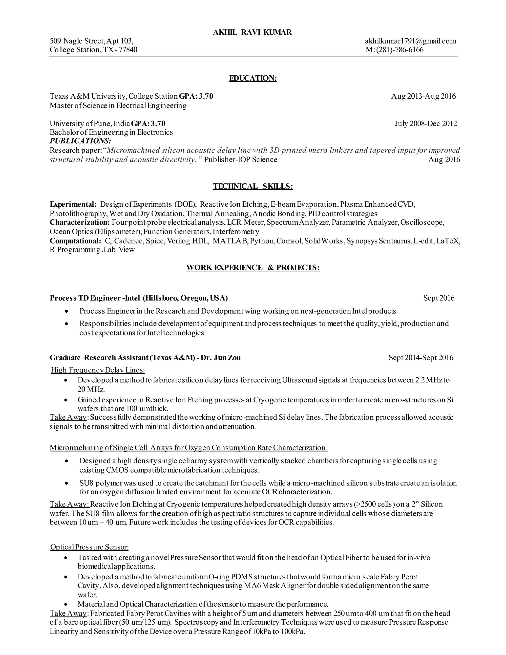
    AKHIL RAVI KUMAR 509Nagle Street,Apt 103, akhilkumar1791@gmail.com College Station,TX-77840 M:(281)-786-6166 EDUCATION: Texas A&M University,College StationGPA:3.70 Aug 2013-Aug 2016 MasterofScience in ElectricalEngineering University ofPune,IndiaGPA:3.70 July 2008-Dec 2012 Bachelorof Engineering in Electronics PUBLICATIONS: Research paper:“Micromachined silicon acoustic delay line with 3D-printed micro linkers and tapered input for improved structural stability and acoustic directivity. ” Publisher-IOP Science Aug 2016 TECHNICAL SKILLS: Experimental: Design ofExperiments (DOE), Reactive Ion Etching,E-beamEvaporation,Plasma EnhancedCVD, Photolithography,Wet andDry Oxidation,Thermal Annealing,Anodic Bonding,PIDcontrolstrategies Characterization: Fourpoint probe electricalanalysis,LCR Meter,SpectrumAnalyzer,Parametric Analyzer,Oscilloscope, Ocean Optics (Ellipsometer),Function Generators,Interferometry Computational: C, Cadence,Spice,Verilog HDL, MATLAB,Python,Comsol,SolidWorks,Synopsys Sentaurus,L-edit,LaTeX, R Programming ,Lab View WORK EXPERIENCE & PROJECTS: Process TDEngineer -Intel (Hillsboro, Oregon,USA) Sept 2016  Process Engineerin the Research and Development wing working on next-generationIntelproducts.  Responsibilities include developmentofequipment andprocess techniques to meet the quality,yield,productionand cost expectationsforInteltechnologies. Graduate ResearchAssistant(Texas A&M) -Dr. JunZou Sept 2014-Sept 2016 High FrequencyDelay Lines:  Developed a methodtofabricatesilicon delaylines forreceivingUltrasoundsignals at frequencies between 2.2MHzto 20 MHz.  Gained experience in Reactive Ion Etching processes at Cryogenic temperatures in orderto create micro-structures on Si wafers that are 100 umthick. Take Away:Successfully demonstratedthe working ofmicro-machined Si delay lines.The fabrication process allowed acoustic signals to be transmitted with minimal distortion andattenuation. Micromachining ofSingle Cell Arrays forOxygen Consumption Rate Characterization:  Designed a high densitysingle cellarray systemwith vertically stacked chambers forcapturingsingle cells using existing CMOS compatible microfabrication techniques.  SU8 polymerwas used to create thecatchment forthe cells while a micro-machined silicon substrate create an isolation for an oxygen diffusion limited environment foraccurate OCRcharacterization. Take Away:Reactive Ion Etching at Cryogenic temperatures helpedcreatedhigh density arrays (>2500 cells)on a 2” Silicon wafer. The SU8 film allows for the creation ofhigh aspect ratio structures to capture individual cells whose diameters are between 10um – 40 um. Future work includes the testing ofdevices forOCR capabilities. OpticalPressure Sensor:  Tasked with creatinga novelPressureSensorthat would fit on the headofan OpticalFiberto be usedforin-vivo biomedicalapplications.  Developed a methodtofabricateuniformO-ring PDMSstructures thatwouldforma micro scale Fabry Perot Cavity.Also,developedalignment techniques using MA6MaskAlignerfordouble sidedalignmentonthe same wafer.  Materialand OpticalCharacterization ofthesensorto measure the performance. Take Away:Fabricated FabryPerot Cavities with a heightof5umand diameters between 250umto 400 umthat fit on the head of a bare opticalfiber(50 um/125 um). Spectroscopyand Interferometry Techniques were used to measure Pressure Response Linearity and Sensitivityofthe Device overa Pressure Rangeof10kPa to 100kPa.
  • 2.
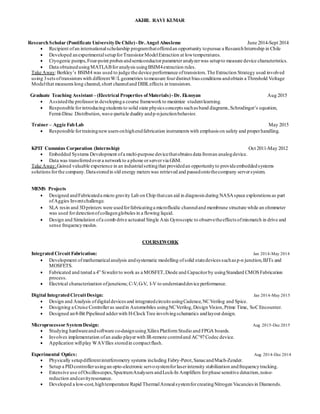
    AKHIL RAVI KUMAR ResearchScholar(Pontificate UniversityDe Chile)-Dr.Angel Abusleme June 2014-Sept 2014  Recipient ofan internationalscholarship programthatofferedan opportunity topursue a ResearchInternship in Chile  Developed anexperimentalsetupforTransistorModelExtraction at lowtemperatures.  Cryogenic pumps,Four-point probes andsemiconductorparameteranalyzerwas setupto measure device characteristics.  Data obtainedusingMATLABforanalysis usingBSIM4extraction rules. Take Away:Berkley’s BSIM4 was used to judge the device performance oftransistors.The Extraction Strategy used involved using 3sets oftransistors with differentW/Lgeometries tomeasure fourdistinct bias conditions andobtain a Threshold Voltage Modelthat measures long channel,short channeland DIBLeffects in transistors. Graduate Teaching Assistant– (Electrical Properties ofMaterials)-Dr. Eknoyan Aug 2015  Assistedthe professorin developinga course frameworkto maximize studentlearning.  Responsible forintroducingstudents to solid state physics concepts suchasband diagrams,Schrodinger’s equation, Fermi-Dirac Distribution,wave-particle duality andp-njunctionbehavior. Trainer – Aggie FabLab May 2015  Responsible fortrainingnewusers onhighendfabrication instruments with emphasis on safety and properhandling. KPIT Cummins Corporation (Internship) Oct 2011-May 2012  Embedded Systems Development ofa multi-purpose devicethatobtains data froman analogdevice.  Data was transferredovera networkto a phone orservervia GSM. Take Away:Gained valuable experience in an industrialsettingthat providedan opportunityto provideembeddedsystems solutions forthe company.Datastoredin old energy meters was retrieved and passedontothecompany serversystem. MEMS Projects  Designed andFabricateda micro gravity Lab on Chip thatcan aid in diagnosis during NASAspace explorations as part ofAggies Inventchallenge.  SLA resin and 3Dprinters were usedforfabricatinga microfluidic channeland membrane structure while an ohmmeter was used fordetectionofcollagenglobules in a flowing liquid.  Design and Simulation ofa comb drive actuated Single Axis Gyroscopic to observetheeffects ofmismatch in drive and sense frequencymodes. COURSEWORK IntegratedCircuitFabrication: Jan 2014-May 2014  Development ofmathematicalanalysis andsystematic modelling ofsolid statedevices suchasp-n junction,BJTs and MOSFETS.  Fabricated and tested a 4” Siwaferto work as a MOSFET,Diode and Capacitorby usingStandard CMOSFabrication process.  Electrical characterization ofjunctions; C-V,G-V, I-V to understanddevice performance. Digital Integrated CircuitDesign: Jan 2014-May 2015  Design and Analysis ofdigitaldevices and integratedcircuits usingCadence,NCVerilog and Spice.  Designing a Cruise Controlleras usedin Automobiles usingNCVerilog,Design Vision,Prime Time, SoCEncounter.  Designed an8-Bit Pipelined adderwith H-ClockTree involvingschematics andlayout design. Microprocessor SystemDesign: Aug 2015-Dec 2015  Studying hardwareandsoftware co-designusingXilinxPlatform Studio and FPGA boards.  Involves implementation ofan audio playerwith IR-remote controland AC’97Codec device.  Application willplay WAVfiles storedin compactflash. Experimental Optics: Aug 2014-Dec 2014  Physically setupdifferentinterferometry systems including Fabry-Perot,SanacandMach-Zender.  Setup a PIDcontrollerusingan opto-electronic servosystemforlaserintensity stabilization andfrequencytracking.  Extensive use ofOscilloscopes,SpectrumAnalysers andLock-In Amplifiers forphase sensitive detection,noise- reduction andcavityresonance.  Developed a low-cost,hightemperature Rapid ThermalAnnealsystemforcreatingNitrogen Vacancies in Diamonds.
  • 3.
    AKHIL RAVI KUMAR DSPbasedmotion control: Jan 2015-May 2015  Study ofelectromechanicalmotion devices with differentcontrolstrategies.  Used Timers,ADC,PWM and QEPmodules in Texas Instrument’s F28035Piccolo microcontrollerto controlthe operation ofBrushlessDCMotors. Certifications  Certified LabviewAssociate Developer-NationalInstruments (NI),April2014  Certified PHPDeveloper  Coursera certificates in Interactive PythonProgramming,Data Scientist’s Toolboxand MathematicalLogic.  Certified Black Belt in IsshinryuKarate. AUTHORIZATION: Authorized to workin the U.S. for OptionalPracticalTraining (OPT)/F-1 VISA(Indian citizenship.
  • 4.