CS3691 Embedded Systems
and IoT
UNIT I 8-BIT EMBEDDED PROCESSOR
8-Bit Microcontroller – Architecture – Instruction Set
and Programming – Programming Parallel
Ports – Timers and Serial Port – Interrupt Handling.
UNIT II EMBEDDED C PROGRAMMING
Memory And I/O Devices Interfacing –Programming
Embedded Systems in C – Need For RTOS Multiple
Tasks and Processes – Context Switching – Priority
Based Scheduling Policies.
UNIT III : IOT AND ARDUINO PROGRAMMING
Introduction to the Concept of IoT Devices – IoT Devices Versus Computers
– IoT Configurations – Basic Components – Introduction to Arduino –
Types of Arduino – Arduino Toolchain – Arduino Programming Structure –
Sketches – Pins – Input/Output From Pins Using Sketches – Introduction to
Arduino Shields – Integration of Sensors and Actuators with
Arduino.
UNIT IV: IOT COMMUNICATION AND OPEN PLATFORMS
IoT Communication Models and APIs – IoT Communication Protocols –
Bluetooth – WiFi – ZigBee – GPS – GSM modules – Open Platform (like
Raspberry Pi) – Architecture – Programming – Interfacing – Accessing
GPIO Pins – Sending and Receiving Signals Using GPIO Pins –
Connecting to the Cloud.
UNIT V: APPLICATIONS DEVELOPMENT
Complete Design of Embedded Systems – Development of IoT
Applications – Home Automation– Smart Agriculture – Smart
Cities – Smart Healthcare.
TEXTBOOK
1. Muhammed Ali Mazidi, Janice Gillispie Mazidi, Rolin D. McKinlay,
“The 8051 icrocontroller and Embedded Systems”, Pearson Education,
Second Edition, 2014
2. Robert Barton, Patrick Grossetete, David Hanes, Jerome Henry, Gonzalo
Salgueiro, “IoT Fundamentals: Networking Technologies, Protocols, and
Use Cases for the Internet of Things”, CISCO Press, 2017.
REFERENCES :
1. Michael J. Pont, “Embedded C”, Pearson Education, 2007.
2. Wayne Wolf, “Computers as Components: Principles of Embedded
Computer System Design”, Elsevier, 2006.
3. Andrew N Sloss, D. Symes, C. Wright, “Arm System Developer’s
Guide”, Morgan Kauffman/ Elsevier, 2006.
4. Arshdeep Bahga, Vijay Madisetti, “Internet of Things – A hands-on
approach”, Universities Press, 2015
COURSE OBJECTIVES:
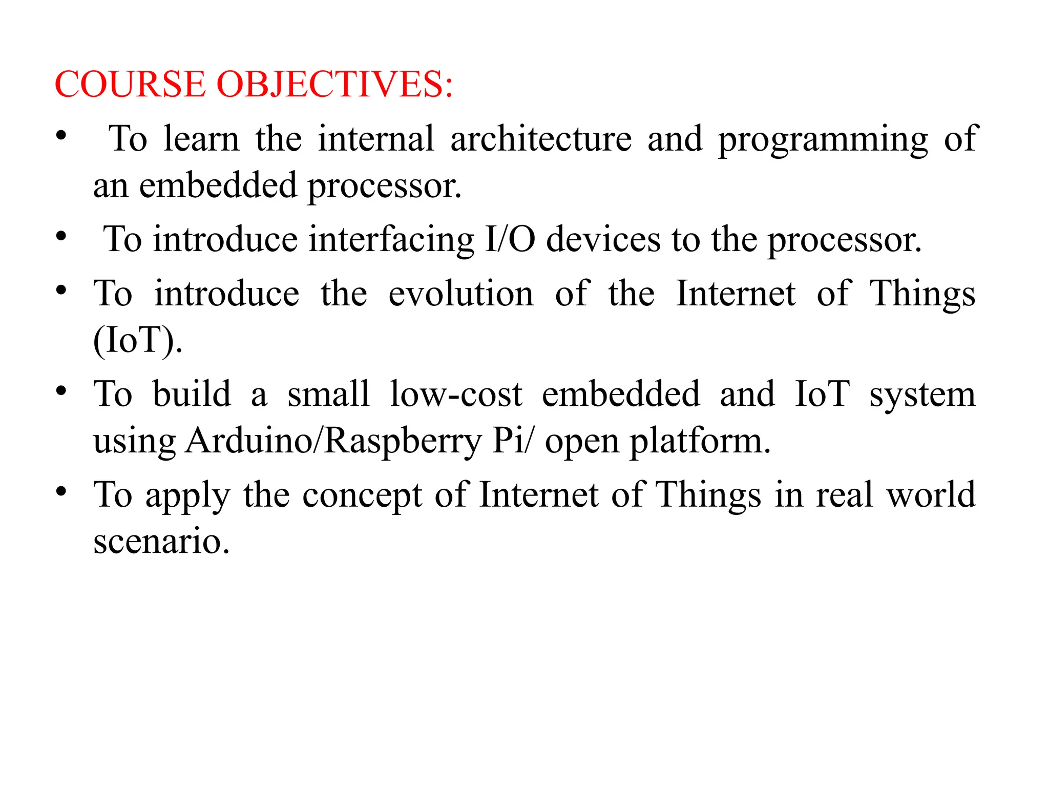
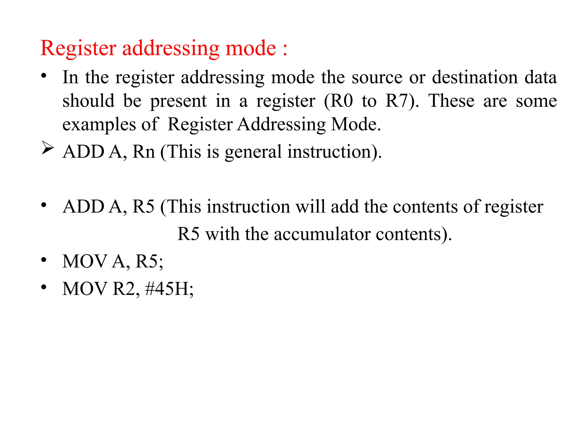
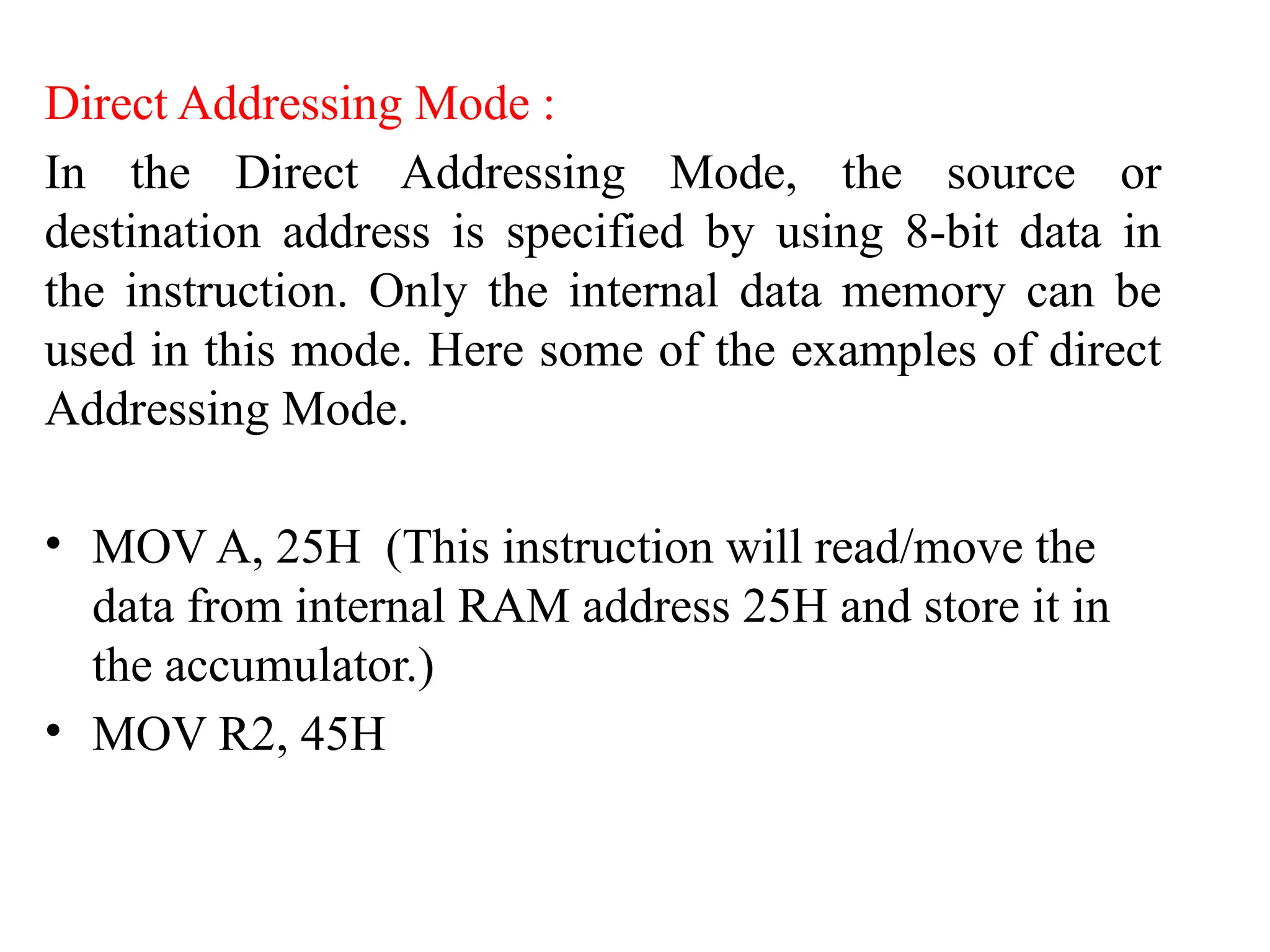
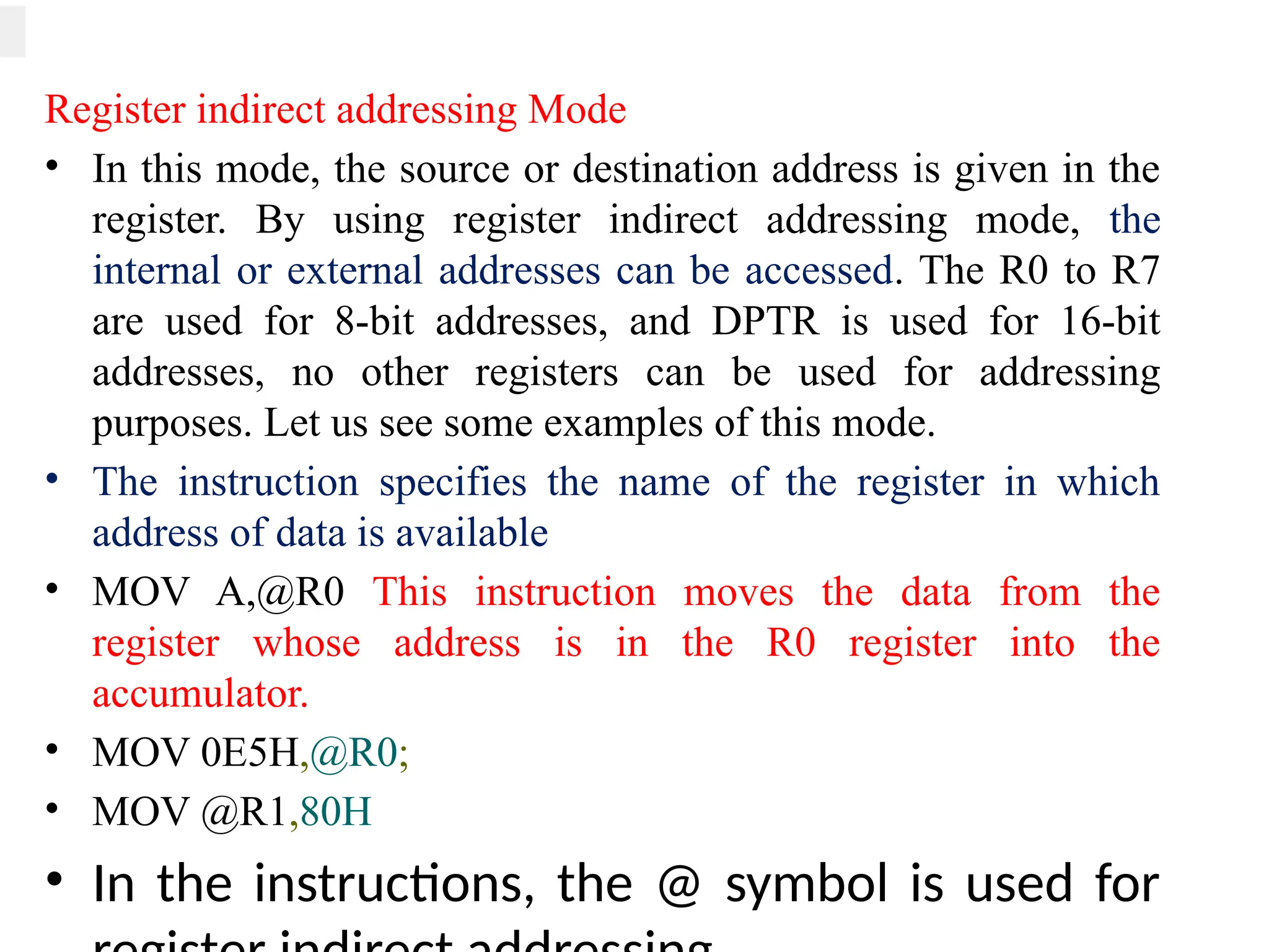
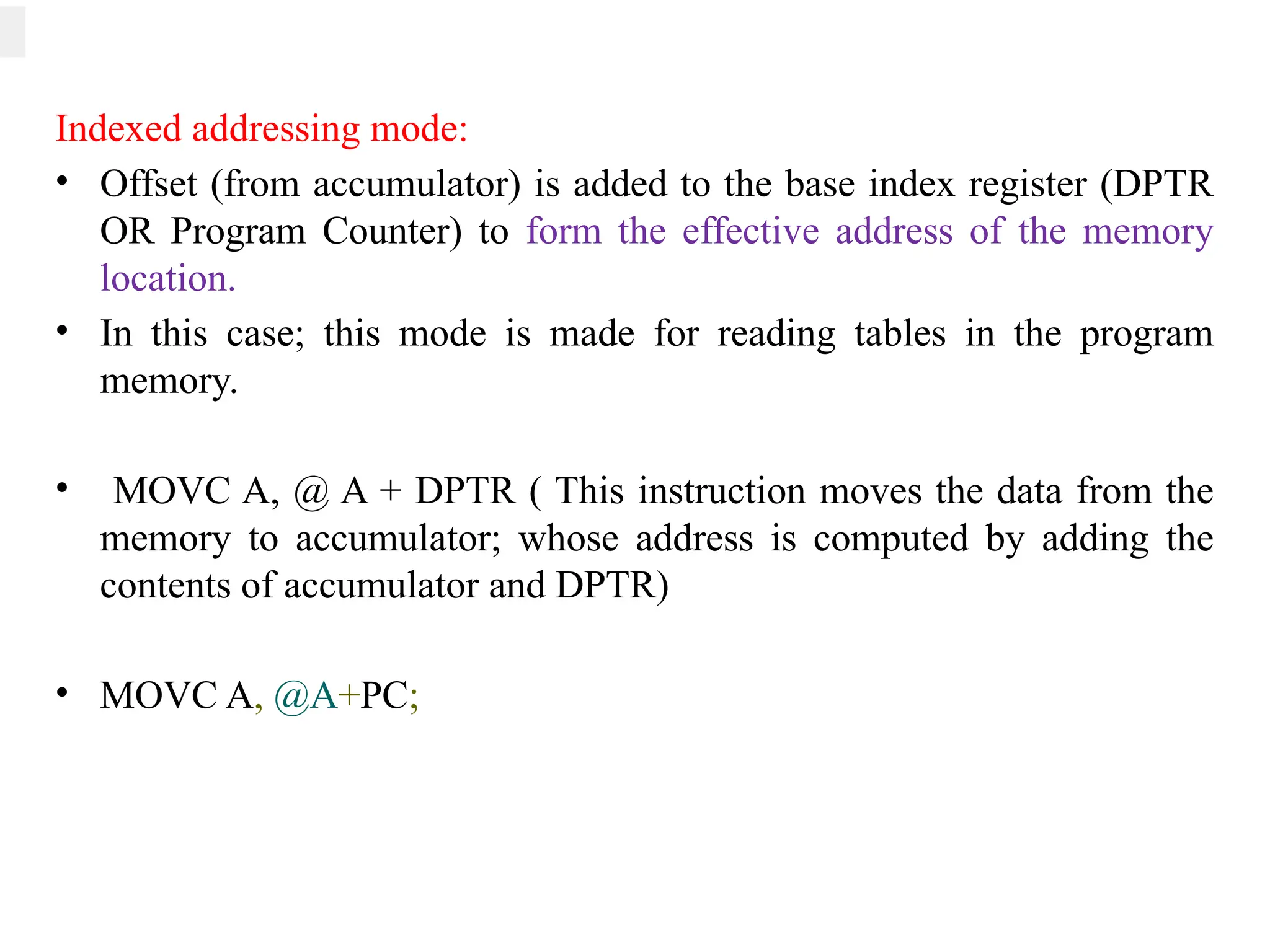
• To learn the internal architecture and programming of
an embedded processor.
• To introduce interfacing I/O devices to the processor.
• To introduce the evolution of the Internet of Things
(IoT).
• To build a small low-cost embedded and IoT system
using Arduino/Raspberry Pi/ open platform.
• To apply the concept of Internet of Things in real world
scenario.
What is a Microprocessor?
• It is a processing device that converts data into
information based on some sets of instructions. It is a very
compact electronic chip due to which it is referred to as
the microprocessor.
OR
• A microprocessor is a computer processor for which the
data processing logic and control is included on a single
integrated circuit (IC), or a small number of Ics
• The microprocessor is used as the CPU (Central
Processing Unit). A typical microprocessor consists of
two major parts namely ALU (Arithmetic Logic Unit)
and CU (Control Unit). Intel 8085 or 8086 processing
chips are the examples of microprocessors.
What is a Microcontroller?
• A microcontroller is an electronic system which
consists of a processing element, a small memory
(RAM, ROM, EPROM), I/O ports, etc. on a single
chip.
• In electronic systems such washing machines,
air conditioners, refrigerators, etc.,
microcontrollers are used to automate the
operation of the device based on user’s
instructions.
S.No Microprocessor Microcontroller
1
Microprocessor acts as a heart of
computer system.
Microcontroller acts as a heart of
embedded system.
2
It is a processor in which memory and
I/O output component is connected
externally.
It is a controlling device in which memory
and I/O output component is present
internally.
3
Since memory and I/O output is to be
connected externally. Therefore the
circuit is more complex.
Since on chip memory and I/O output
component is available. Therefore the
circuit is less complex.
4
It cannot be used in compact system.
Therefore microprocessor is
inefficient.
It can be used in compact system.
Therefore microcontroller is more
efficient.
5
Microprocessor has less number of
registers. Therefore most of the
operations are memory based.
Microcontroller has more number of
registers. Therefore a program is easier to
write.
6
A microprocessor having a zero status
flag.
A microcontroller has no zero flag.
7
It is mainly used in personal
computers.
It is mainly used in washing machines, air
conditioners etc.
On the basis of architecture the types of
microcontroller are:
Von Neumann architecture:
• In a Von Neumann architecture, instructions and data are
stored in a single memory system. This memory is usually
implemented as random access memory (RAM) and is
connected to the CPU and I/O devices through a common bus.
Havard Architecture:
•Harvard architecture is a type of computer architecture that has
separate memory spaces for instructions and data.
•In a Harvard architecture system, the CPU accesses instruction
and data memory spaces separately, which can lead to improved
performance.
Types of Microcontroller on the basis of Service
Provider
AVR microcontroller is developed by Atmel
service provider.
Peripheral Interface Controller
8051 Microcontroller Architecture:
• 4 KB on-chip ROM (Program memory).
• 128 bytes on-chip RAM (Data memory).
• The 8-bit data bus (bidirectional).
• 16-bit address bus (unidirectional).
• Two 16-bit timers.
• Instruction cycle of 1 microsecond with 12 MHz crystal.
• Four 8-bit input/output ports.
• 128 user-defined flags.
• Four register banks of 8 bit each.
• 16-byte bit-addressable RAM.
• The general purpose registers are 32 each is 8-bit.
• 8051 has two external and three internal interrupts.
• 8051 microcontroller specifies some special function features like UARTs,
ADC, Op-amp, etc.
•It has a 16-bit program counter and data pointer.
Key features of the 8051 Microcontroller:
Arithmetic and Logic Unit (ALU):
• All arithmetic and logical functions are carried out by the ALU.
• Addition, subtraction with carry, and multiplication come under arithmetic
operations.
• Logical AND, OR and EXOR come under logical operations.
Program Counter(PC):
• A program counter is a 16-bit register .
• The basic function of program counter is to fetch the next instruction to be executed.
The PC increments automatically, holding the address of the next instruction.
Accumulator (A) and B Registers:
• Registers are usually known as data storage devices. 8051 microcontroller has 2
registers, namely Register A and Register B. These registers are used to store
the output of mathematical and logical operations. B register is mainly used
for multiplication and division operation along with A register.
• The Accumulator or Register A: is the most important and
most used 8051 Microcontroller SFRs.
• The Accumulator is used to hold the data for almost all the
ALU Operations.
• Some of the operations where the Accumulator is used are:
• Arithmetic Operations like Addition, Subtraction,
Multiplication etc.
• Logical Operations like AND, OR, NOT etc.
• Data Transfer Operations (between 8051 and External
Memory)
Stack pointer (SP):
The stack pointer in the 8051 holds the 8-bits address at
the top of the stack, it supports the LIFO(Last In First
Out) and it can take a value of 00 to FFH. The stack can
be accessed using PUSH and POP instructions.
DPTR (Data pointer) Register:
DPTR is a 16 bit register used to hold the 16 bit
address of data memory. The 16 bit data pointer can
also be used as two 8 bit data pointer namely DPH,
DPL. 8 bit data pointer used to accessing RAM and
SFR.
Bus :
Bus is a group of wires which uses as a communication canal or
acts as means of data transfer. The different bus configuration
includes 8, 16 or more cables. Therefore, a bus can bear 8 bits, 16
bits all together.
Types of buses in 8051 Microcontroller:
Let's see the two types of bus used in 8051 microcontroller:
Address Bus: 8051 microcontrollers is consisting of 16 bit address
bus. It is generally be used for transferring the data from Central
Processing Unit to Memory.
Data bus: 8051 microcontroller is consisting of 8 bits data bus. It is
generally be used for transferring the data from one peripherals
position to other peripherals.
Program Status Word Register (PSW):
• Program Status Word Register is also called as Flag Register and
is one of the important Special function Register (SFRs).
• The PSW Register consists of Flag Bits, which help the
programmer in checking the condition of the result and also make
decisions.
• Flags are 1-bit storage elements that store and indicate the nature
of the result that is generated by execution of certain instructions.
The following image shows the contents of the PSW Register.
• Parity Bit (P)
– This parity flag bit is used to show the number of 1s in the accumulator
only. If the accumulator register contains an odd number of 1s, then this
flag set to 1.
– If accumulator contains even number of 1s, then this flag cleared to 0.
• Overflow Flag (OV)
– This flag is set during ALU operations, to indicate overflow in the result. It
is set to 1 if there is a carry out of either the D7 bit or the D6 bit of the
accumulator.
– Overflow flag is set when arithmetic operations such as add and subtract
result in sign conflict.
Register Bank Select Bits (RS1 And RS0)
– These two bits are used to select one of four register banks of RAM. By
setting and clearing these bits, registers R0-R7 are stored in one of four
banks of RAM as follows.
Program Status Word Register (PSW)…
• General-Purpose Flag (F0)
– This is a user-programmable flag; the user can program and
store any bit of his/her choice in this flag, using the bit
address.
• Auxiliary Carry Flag (AC)
– It is used in association with BCD arithmetic. This flag is set
when there is a carry out of the D3 bit of the accumulator.
• Carry Flag (CY)
– This flag is used to indicate the carry generated after arithmetic
operations. It can also be used as an accumulator, to store one
of the data bits for bit-related Boolean instructions.
Program Status Word Register (PSW)…
Input/Output (I/O) Ports:
• The I/O ports of the 8051 microcontroller are used to interface with the
outside world. The 8051 microcontroller has four ports, each of which can
be configured as either input or output. The ports are named Port 0, Port 1,
Port 2, and Port 3.
• Port 0 is an 8-bit bidirectional port that can be used to interface with external
devices.
• Port 1 is also an 8-bit bidirectional port that can be used to interface with
external devices.
• Port 2 is an 8-bit port that is used to interface with external memory devices.
• Port 3 is an 8-bit port that is used to interface with external interrupt sources.
• In addition to the four I/O ports, the 8051 microcontroller also has several
other I/O pins, including the Reset pin, the XTAL1 and XTAL2 pins, and the
ALE (Address Latch Enable) pin. These pins are used for various purposes,
such as system reset, clock input, and address bus control.
Data Memory:
• The data memory of the 8051 microcontroller is used to store data that is
used by the microcontroller during operation. The data memory can be
either internal RAM or external RAM.
• The size of the data memory varies from 128 bytes to 256 bytes for
internal RAM, and up to 64K bytes for external RAM.
• The data memory is divided into two sections: the general-purpose
registers and the SFRs (special function registers).
• The general-purpose registers are used to store data during program
execution, while the SFRs are used to control the operation of the
microcontroller and to interface with external devices.
Program Memory:
 The program memory of the 8051 microcontroller is used to store the
program code that the microcontroller executes. The program memory
can be either ROM or Flash memory.
 The size of the program memory varies from 2K to 64K bytes,
depending on the specific model of the microcontroller.
SCON (Serial Control) Register:
• The Serial Control or SCON SFR is used to control the 8051
Microcontroller’s Serial Port. It is located as an address of
98H. SCON, control the Operation Modes of the Serial Port.
• SCON Register also consists of bits that are automatically
SET when a byte of data is transmitted or received.
Power Control (PCON) Register:
IDLE MODE:
In this mode the clock is cut from the processor only, other parts of the
microcontroller such as timers. In this mode 80% of power is saved. The 20%
power is used to get the microcontroller from idle mode to normal mode.
POWER DOWN MODE:
In this mode, clock supply is cut from the whole system. In this power saving
mode maximum amount of power is saved.
The PCON register is used for power control and baud rate selection.It also
consists of general purpose user flags.
TCON (Timer Control register):
TCON is an 8-bit register. Its bits are used for generating
interrupts internal or external. The most important bits of the
timer TR and TF are also in it. TR (timer run) and TF (timer
overflow) bits which we use in almost all over timer
applications are in it.
TMOD (Timer Mode register):
• 8-bit register used to select timer mode. There are 4 modes in which timer can be
loaded.
1. Mode 0 : 13-bit timer
2. Mode 1: 16-bit timer
3. Mode 2 : 8-bit auto reload
4. Mode 3 : Split timer mode
• TH0/TL0->Timer 0 :16 bit register (byte addressable only) 8 bits can be send at a
time.
• TH1/TL1-> Timer 1: 16 bit register (byte addressable only) 8 bits can be send at a
time.
The TMOD register is used to select the operating mode and the timer/Counter
operation. The Lower 4 bits used to control timer 0 and the upper two bits used
to control timer 1.
C/T – 0 TIMER
- 1 Counter
IE (Interrupt Enable) Register:
• This register is responsible for enabling and disabling the
interrupt. EA register is set to one for enabling interrupts
and set to 0 for disabling the interrupts. Its bit sequence
and their meanings are shown in the following figure.
IP (Interrupt Priority) Register:
• We can change the priority levels of the interrupts by changing
the corresponding bit in the Interrupt Priority (IP) register as
shown in the following figure.
• A low priority interrupt can only be interrupted by the high
priority interrupt, but not interrupted by another low priority
interrupt.
• If two interrupts of different priority levels are received
simultaneously, the request of higher priority level is served.
• If the requests of the same priority levels are received
simultaneously, then the internal polling sequence determines
which request is to be serviced.
Timer and Control Unit:
• The main function of a timer is to make a delay otherwise
time gap among two events.
• This microcontroller includes two timers where each
timer is 16-bit where the system can generate two delays
concurrently to produce the suitable delay.
• The delay can be generated through the timer based on
the requirement of the processor & transmits the signal to
the processor whenever the particular delay gets
generated.
Types of interrupt in 8051 Microcontroller:
• Timer 0 overflow interrupt - TF0
• Timer 1 overflow interrupt - TF1
• External hardware interrupt - INT0
• External hardware interrupt - INT1
• Serial communication interrupt - RI/TI
8051 microcontroller Pin Diagram :
8051 microcontroller is a 40
pin Dual Inline Package (DIP).
These 40 pins serve different
functions like read, write, I/O
operations, interrupts etc.,
8051 has four I/O ports
wherein each port has 8 pins
which can be configured as
input or output depending
upon the logic state of the
pins. Therefore, 32 out of
these 40 pins are dedicated to
I/O ports. The rest of the pins
are dedicated to VCC, GND,
XTAL1, XTAL2, RST, ALE,
EA’ and PSEN
• Port 0 (P0.1 – P0.7) - Pin 32 to Pin 39 : This is an 8-bit
bidirectional input/output pins. The output drives and inputs buffers
of port 0 are used to access external memory.
• Port 1 (P1.0-P0.7) - Pin 1 to Pin 8 – Pin 1 to Pin 8 are assigned to
Port 1 for simple I/O operations. They can be configured as input or
output pins depending on the logic control i.e. if logic zero (0) is
applied to the I/O port it will act as an output pin and if logic one (1)
is applied the pin will act as an input pin. These pins are also
referred to as P1.0 to P1.7
• // (where P1 indicates that it is a pin in port 1 and the number after
‘.’ tells the pin number i.e. 0 indicates first pin of the port. So, P1.0
means first pin of port 1, P1.1 means second pin of the port 1 and so
on). These pins are bidirectional pins.//
• Port 2 (Pin 21 to Pin 28) – Pin 21 to pin 28 are port 2 pins also
referred to as P2.0 to P2.7. When additional external memory is
interfaced with the 8051 microcontroller, pins of port 2 act as
higher-order address bytes. These pins are bidirectional.
Port 3 (Pin 10 to Pin 17)– Pin 10 to pin 17 are port 3 pins which are also referred to
as P3.0 to P3.7. These pins are similar to port 1 and can be used as universal input or
output pins. These pins are bidirectional pins. These pins also have some additional
functions which are as follows:
– P3.0 (RXD) : 10th pin is RXD (serial data receive pin) which is for serial
input. Through this input signal microcontroller receives data for serial
communication.
– P3.1 (TXD) : 11th pin is TXD (serial data transmit pin) which is serial output
pin. Through this output signal microcontroller transmits data for serial
communication.
– P3.2 and P3.3 (INT0′, INT1′ ) : 12th and 13th pins are for External Hardware
Interrupt 0 and Interrupt 1 respectively. When this interrupt is activated (i.e.
when it is low), 8051 gets interrupted in whatever it is doing and jumps to the
vector value of the interrupt (0003H for INT0 and 0013H for INT1) and starts
performing Interrupt Service Routine (ISR) from that vector location.
– P3.4 and P3.5 (T0 and T1) : 14th and 15th pin are for Timer 0 and Timer 1
external input. They can be connected with 16 bit timer/counter.
– P3.6 (WR’) : 16th pin is for external memory write i.e. writing data to the
external memory.
– P3.7 (RD’) : 17th pin is for external memory read i.e. reading data from
external memory.
• Pin 9 (RST) – Reset pin. It is an active-high, input pin. Therefore if
the RST pin is high for a minimum of 2 machine cycles, the
microcontroller will reset i.e. it will close and terminate all
activities. It is often referred as “power-on-reset” pin because it is
used to reset the microcontroller to it’s initial values when power is
on (high).
• Pin 18 and Pin 19 (XTAL2 And XTAL1) – These pins are
connected to an external oscillator which is generally a quartz
crystal oscillator. They are used to provide an external clock
frequency of 4MHz to 30MHz.
• Pin 20 (GND) – This pin is connected to the ground. It has to be
provided with 0V power supply. Hence it is connected to the
negative terminal of the power supply.
• Pin 29 (PSEN) – PSEN stands for Program Store Enable. It is
output, active-low pin. This is used to read external memory. In
8031 based system where external ROM holds the program code,
this pin is connected to the OE pin of the ROM.
• Pin 30 (ALE/ PROG) – ALE stands for Address Latch Enable. It is
input, active-high pin. This pin is used to distinguish between memory
chips when multiple memory chips are used. It is also used to de-
multiplex the multiplexed address and data signals available at port 0.
During flash programming i.e. Programming of EPROM, this pin acts as
program pulse input (PROG).
• Pin 31 (EA/ VPP) – EA stands for External Access input. It is used to
enable/disable external memory interfacing. In 8051, EA is connected to
VCC as it comes with on-chip ROM to store programs.
• Pin 40 (VCC) – This pin provides power supply voltage i.e. +5 Volts to
the circuit.
Addressing modes of 8051
• Immediate Addressing Mode
• Register Addressing Mode
• Direct Addressing Mode
• Register Indirect Addressing Mode
• Indexed Addressing Mode
• Implied Addressing Mode
The way in which an operand is given to an instruction is known
as addressing modes. Different addressing modes of the 8051
microcontrollers. In 8051 there are 1-byte, 2-byte instructions and
very few 3-byte instructions are present. The opcodes are 8-bit
long. As the opcodes are 8-bit data, there are 256 possibilities.
Immediate addressing mode :
• In this Immediate Addressing Mode, the data is provided in
the instruction itself. The data is provided immediately after
the opcode. These are some examples of Immediate
Addressing Mode.
MOV A, #0AFH;
MOV R3, #45H;
MOV DPTR, #FE00H
• In these instructions, the # symbol is used for immediate data.
In the last instruction, there is DPTR. The DPTR stands for
Data Pointer. Using this, it points the external data memory
location
Register addressing mode :
• In the register addressing mode the source or destination data
should be present in a register (R0 to R7). These are some
examples of Register Addressing Mode.
 ADD A, Rn (This is general instruction).
• ADD A, R5 (This instruction will add the contents of register
R5 with the accumulator contents).
• MOV A, R5;
• MOV R2, #45H;
Direct Addressing Mode :
In the Direct Addressing Mode, the source or
destination address is specified by using 8-bit data in
the instruction. Only the internal data memory can be
used in this mode. Here some of the examples of direct
Addressing Mode.
• MOV A, 25H (This instruction will read/move the
data from internal RAM address 25H and store it in
the accumulator.)
• MOV R2, 45H
Register indirect addressing Mode
• In this mode, the source or destination address is given in the
register. By using register indirect addressing mode, the
internal or external addresses can be accessed. The R0 to R7
are used for 8-bit addresses, and DPTR is used for 16-bit
addresses, no other registers can be used for addressing
purposes. Let us see some examples of this mode.
• The instruction specifies the name of the register in which
address of data is available
• MOV A,@R0 This instruction moves the data from the
register whose address is in the R0 register into the
accumulator.
• MOV 0E5H,@R0;
• MOV @R1,80H
• In the instructions, the @ symbol is used for
Indexed addressing mode:
• Offset (from accumulator) is added to the base index register (DPTR
OR Program Counter) to form the effective address of the memory
location.
• In this case; this mode is made for reading tables in the program
memory.
• MOVC A, @ A + DPTR ( This instruction moves the data from the
memory to accumulator; whose address is computed by adding the
contents of accumulator and DPTR)
• MOVC A, @A+PC;
Implied Addressing Mode:
• In the implied addressing mode, there will be a single operand.
These types of instruction can work on specific registers only.
These types of instructions are also known as register specific
instruction. Here are some examples of Implied Addressing
Mode.
RLA;
SWAP A;
Types of instructions:-
Depending on operation they perform, all instructions are
divided in several groups:
• Data Transfer Instructions
• Arithmetic Instructions
• Logic Instructions
• Data exchange
• Push and Pop Instructions
• Rotate and Swap Instructions
• Bit-oriented Instructions
• Branch Instructions
Data Transfer Instructions:-
• Data transfer instructions move the content of one
register to another.
• The register the content of which is moved remains
unchanged.
• Data can be transferred within the internal Memory/to
and from external RAM.
• If they have the suffix “X” (MOVX), the data is
exchanged with external memory.
Data Transfer Instructions…
Instruction to Access External Data Memory:
Arithmetic Instructions:
Mnemonics Description Bytes Instruction Cycles
ADD A, Rn AA + Rn (Add register to Accumulator) 1 1
ADD A, direct AA + (direct) (Add direct byte to Accumulator) 2 1
ADD A, @Ri AA + @Ri(Add indirect RAM to Accumulator) 1 1
ADD A, #data AA + data (Add immediate data to Accumulator) 2 1
ADDC A, Rn AA + Rn + C (Add register to Accumulator with Carry) 1 1
ADDC A, direct A A + (direct) + C (Add direct byte to Accumulator with Carry) 2 1
ADDC A, @Ri AA + @Ri + C (Add indirect RAM to Accumulator with Carry) 1 1
ADDC A, #data AA + data + C (Add immediate data to Acc with Carr) 2 1
SUBB A, Rn AA - Rn - C (Accumulator Subtract Register from Acc with borrow) 1 1
SUBB A, direct AA - (direct) - C (Subtract direct byte from Acc with borrow) 2 1
SUBB A, @Ri AA - @Ri - C (Subtract indirect RAM from ACC with borrow) 1 1
SUBB A, #data AA - data - C (Subtract immediate data from Acc with borrow) 2 1
DIV AB
Divide A by B (Divide A by B)
A quotient
B remainder
1 4
MUL AB
Multiply A by B (Multiply A & B)
A low byte (A*B)
B high byte (A* B)
1 4
INCREMENT & DECREMNT INSTRUCTIONS
INC A AA+1 (Increment Accumulator) 1 1
INC Rn Rn Rn + 1 (Increment register) 1 1
INC direct (direct) (direct) + 1 (Increment direct byte) 2 1
INC @Ri @Ri @Ri +1 (Increment direct RAM) 1 1
INC DPTR DPTR DPTR +1 (Increment Data Pointer) 1 2
DEC A AA -1 (Decrement Accumulator) 1 1
DEC Rn Rn Rn - 1 (Decrement Register) 1 1
DEC direct (direct) (direct) - 1 (Decrement direct byte) 2 1
DEC @Ri @Ri @Ri - 1 (Decrement indirect RAM) 1 1
DAA Decimal Adjust (Decimal Adjust Accumulator) 1 1
Logic Instructions :
Bit Level Logical Instructions:
Push and Pop Instructions:
Data Exchange instructions:
Programming Parallel Ports
• The 8051 microcontroller has four parallel I/O ports,
each of 8-bits. So, it provides the user 32 I/O lines
for connecting the microcontroller to the peripherals.
• The four ports are P0 (Port 0), P1(Port1),P2(Port 2)
and P3 (Port3).
• Upon reset all the ports are output ports.
• In order to make them input, all the ports must
be set i.e a high bit must be sent to all the port
pins. This is normally done by the instruction
“SETB”.
Ex: MOV A,#0FFH ; A = FF
MOV P0,A ; make P0 an input port
PORT 0:
• Port 0 is an 8-bit I/O port with
dual purpose. If external memory
is used, these port pins are used
for the lower address byte
address/data (AD0-AD7),
otherwise all bits of the port are
either input or output. Unlike
other ports, Port 0 is not provided
with pull-up resistors internally ,so
for PORT0 pull-up resistors of
nearly 10k are to be connected
externally as shown.
ALE indicates whether P0 has address or data. When ALE = 0, it
provides data D0-D7 and when ALE =1 it provides address and data
Port 1:
• Port 1 occupies a total of 8 pins (pins 1 through 8). It
has no dual application and acts only as input or
output port. In contrast to port 0, this port does not
need any pull-up resistors since pull-up resistors
connected internally. Upon reset, Port 1 is configured
as an output port. To configure it as an input port,
port bits must be set i.e a high bit must be sent to all
the port pins. This is normally done by the instruction
“SETB”.
Ex:
MOV A, #0FFH; A=FF HEX
MOV P1, A; make P1 an input port by writing 1’s to all
of its pins
Port 2:
• Port 2 is also an eight-bit parallel port. (pins 21- 28).
It can be used as input or output port. As this port is
provided with internal pull-up resistors it does not
need any external pull-up resistors.
• Upon reset, Port 2 is configured as an output port. If
the port is to be used as input port, all the port bits
must be made high by sending FF to the port.
For Ex:
MOV A, #0FFH ; A=FF hex
MOV P2, A ; make P2 an input port by writing all
1’s to it
PORT 3:
• Port3 is also an 8-bit parallel port with dual function. (pins 10
to 17). The port pins can be used for I/O operations as well as
for control operations. The details of these additional operatio
• ns are given below in the table. Port 3 also do not need any
external pull-up resistors as they are provided internally
similar to the case of Port2 & Port 1. Upon reset port 3 is
configured as an output port. If the port is to be used as input
port, all the port bits must be made high by sending FF to the
port.
• MOV A, #0FFH ; A= FF hex
• MOV P3, A ; make P3 an input port by writing all 1’s to it
TIMER’S CLOCK FREQUENCY AND ITS PERIOD
• In 8051-based system, the crystal oscillator has a frequency of
11.0592 MHz when C/T bit of TMOD is 0. Each machine
cycle is made up of 12 clock cycles.
• Hence for a single machine cycle, the frequency becomes
1/12 × 11.0529 MHz = 921.6 KHz.
• For a single machine cycle, the time taken is
T = 1/921.6 KHz = 1.085 us
• so the oscillator takes 1.085us for completing a single machine
cycle.
MODE 0 :
• Mode 0 is exactly same like mode 1 except that it is a
13-bit timer instead of 16-bit. The 13- bit counter can
hold values between 0000 to 1FFFH in TH-TL.
• Therefore, when the timer reaches its maximum of
1FFH, it rolls over to 0000, and TF is raised.
MODES OF OPERATION:
MODE 1:
• It is a 16-bit timer; therefore it allows values from 0000 to FFFFH to be loaded
into the timer’s registers TL and TH as shown in Fig.
• After TH and TL are loaded with a 16-bit initial value, the timer must be
started. We can do it by “SETB TR0” for timer 0 and “SETB TR1” for timer 1.
• After the timer is started, it starts count up until it reaches its limit of FFFFH.
When it rolls over from FFFF to 0000H, it sets high a flag bit called TFx
(timer flag).
• This timer flag can be monitored. When this timer flag
is raised, one option would be stop the timer with the
instructions “CLR TR0“ or CLR TR1 for timer 0 and
timer 1 respectively. Again, it must be noted that each
timer flag TF0 for timer 0 and TF1 for timer1.
• After the timer reaches its limit and rolls over, in order
to repeat the process the registers TH and TL must be
reloaded with the original value and TF must be reset
to 0.
MODE 2:
• It is an 8 bit timer that allows only values of 00 to FFH to be
loaded into the timer’s register TH as shown in Figure.
• After THx is loaded with 8 bit value, the 8051 gives a copy of
it to TLx. Then the timer must be started. It is done by the
instruction “SETB TR0” for timer 0 and “SETB TR1” for
timer1. This is like mode 1.
• After timer is started, it starts to count up by incrementing the TLx
register. It counts up until it reaches its limit of FFH. When it rolls
over from FFH to 00, it sets high the TFx (timer flag).
 If we are using timer 0, TF0 goes high; if using TF1 then TF1 is raised.
• When TLx register rolls from FFH to 00 and TF is set to 1, TLx is
reloaded automatically with the original value kept by the THx
register.
• To repeat the process, we must simply clear TFx and let it go
without any need by the programmer to reload the original value.
This makes mode 2 auto reload, in contrast in mode 1 in which
programmer has to reload THx and TLx.
MODE 2…
MODE 3:
• Mode 3 is also known as a split timer mode. Timer 0
and 1 may be programmed to be in mode 0, 1 and 2
independently of similar mode for other timer. This is
not true for mode 3.
• Timers do not operate independently if mode 3 is
chosen for timer 0. Placing timer 1 in mode 3 causes
it to stop counting; the control bit TR1 and the timer
1 flag TF1 are then used by timer 0.
Example:
Generate Delay =10ms with Clock frequency= 11.0592 MHz, using
Timer 0 in mode1.
Solution:
Time delay=10ms; Clock frequency=11.0592 MHz
Step 1: Divide the desired time delay by 1.085 us
Count =10 ms/1.085 us= 9216
Step 2: Perform 65536 – n
65536-9216=56320= DC00H
Step 3: Set TL = xx and TH = yy
Here xx=DC and yy=00, Hence, TH0=DC and TL0=00.
The assembly code program to generate a delay
of 10ms
MOV TMOD, #01 ;Timer 0, mode 1, 16-bitmode
HERE: MOV TL0, #00 ;TL0=0, the low byte
MOV TH0,#0DCH ;TH0=DC, the high byte
SETB TR0 ;Start timer 0
AGAIN: JNB TF0,AGAIN ;Monitor timer flag 0
CLR TR0 ;Stop the timer 0
CLR TF0 ;Clear timer 0 flag
Program to generate a square wave of 5 kHz
frequency on pin P1.0, clock frequency =11.0592 MHz
Given:
Square wave frequency=5 kHz
Clock frequency=11.0592 MHz
Step 1: Calculate the Time delay
T=1/f=1/5 kHz =0.2 ms
T=0.2 ms which is the period of square wave
T/2 =0.2/2=0.1 ms delay for high and low
Step 2: Divide the desired time delay by 1.085 us
Count=0.1ms/1.085 us = 92
Step 3: Perform 65536 – n
TH0-TL0= 65536-92=65444= FFA4 H
MOV TMOD,#10 ;Timer 1, mode 1, 16-bitmode
AGAIN: MOV TL1,#A4H ;TL1=A4, low byte of timer
MOV TH1,#0FFH ;TH1=FF, the high byte
SETB TR1 ;Start timer
BACK: JNB TF1,BACK ;until timer rolls over
CPL P1.0 ; compliment P1.0
CLR TR1 ;Stop the timer 1
CLR TF1 ;Clear timer 1 flag
SJMP AGAIN ;Reload timer
Toggle LED connected at P1.0 with 5
microsec delay using timer1 and mode 2
MOV TMOD,#20 ;Timer 1 mode 2, 8-bit auto reload
AGAIN: MOV TH1,#-5 ;TL1=256-5, low byte of timer
SETB TR1 ;Start timer 1
BACK: JNB TF1, BACK ;until timer rolls over
CPL P1.0 ; compliment P1.0 toggle LED
CLR TF1 ;Stop the timer 1
SJMP BACK
Serial Ports in 8051 Microcontroller
• Microcontrollers can communicate data in either parallel form or
serial form.
• In parallel communication, data is transferred over more than
one wire for example if 8 wires of one microcontroller are
connected to any other peripheral device or another
microcontroller then at a particular time 8 data bits are
transferred.
• On the other hand, in serial communication, data is transferred
in bit by bit manner over a single wire.
• Serial communication is preferred when the distance between
transmitter and receiver is large and it is required to save the
cabling cost and reduce hardware complexity but definitely this
comes at the cost of reduced speed of data transfer.
Fig. shows parallel data transmission
Fig. shows serial data transmission
In 8051 in built UART
(Universal Asynchronous
Receiver Transmitter) module
performs the job of serial
communication of data.
In 8051 microcontroller serial communication of data is
performed with the help of following special purpose
registers:
• SBUF (Serial buffer register)
• SCON (serial control register)
• TMOD (Timer mode register)
• TCON (Timer control register)
• TH1 (Timer1 register higher byte)
SBUF (Serial buffer register) :
• It is an 8-bit register and is used for serial communication of
data in 8051 microcontroller.
• Whatever data is required to be transmitted via TXD line must be
placed in the SBUF register.
• Similarly, the received data via RXD line is saved in SBUF
register.
• When data is written to SBUF register then it is framed in
between start and stop bit before it is transmitted via TXD line
and similarly during reception of data start and stop bits are
removed and actual data bits are extracted from the received
frame and then it is placed in the SBUF register.
SCON (Serial Control) Register:
• The Serial Control or SCON SFR is used to control the 8051 Microcontroller’s
Serial Port. It is located as an address of 98H. SCON, control the Operation
Modes of the Serial Port.
• SCON Register also consists of bits that are automatically SET when a byte of
data is transmitted or received.
Example: set baud rate at 9600
MOV TMOD, #20H ; timer 1,mode 2(auto reload)
MOV TH1, #-3 ; To set 9600 baud rate
SETB TR1 ; start timer 1
For the crystal oscillator frequency of 11.0592MHz the below given
table can be used as a reference for getting the value that is required
to be loaded into TH1 register for the desired baud rate generation.
Baud Rate TH1 (Decimal) TH1 (Hex)
9600 -3 FD
4800 -6 FA
2400 -12 F4
1200 -24 E8
Write a program for the 8051 to transfer letter ‘A’ serially
a 4800 baud rate continuously.
MOV TMOD, #20H ; Timer 1, Mode 2 (Auto reload)
MOV TH1, #-6 ; 4800 baud rate
MOV SCON, #50H ; 8-bit, 1 stop, REN enabled
SETB TR1 ; Star Timer 1
AGAIN: MOV SBUF, # “A” ; Letter A to be transferred
HERE: JNB TI HERE
CLR T1 ; Clear TI for next char
SJMP AGAIN
Write a program to transfer the message “YES” serially at 9600 baud rate, 8-bit data, 1 stop
bit. Do this continuously.
MOV TMOD, #20H ;Timer 1, Mode 2 (Auto reload)
MOV TH1, #FD ; 9600 baud rate
MOV SCON, #50H ; 8-bit, 1 stop, REN enabled
SETB TR1 ; Star Timer 1
AGAIN: MOV A, #”Y” ; transfer Y
ACALL TRANS
MOV A, #”E” ; transfer E
ACALL TRANS
MOV A, #”S” ; transfer S
ACALL TRANS
SJMP AGAIN
TRANS: MOV SBUF, A ; Load SBUF
HERE: JNB TI, HERE ; wait for last bit to transfer
RET
Write a program for the 8051 to receive byte of data serially, and
put them in P1. Set the 4800 baud rate, 8-bit data and 1 stop bit.
MOV TMOD, #20H ;Timer 1, Mode 2 (Auto reload)
MOV TH1, #-6 ; 4800 baud rate
MOV SCON, #50H ; 8-bit, 1 stop, REN enabled
SETB TR1 ; Star Timer 1
HERE: JNB RI, HERE ; wait for char to come
MOV A, SBUF;save incoming byte in A
MOV P1, A ;sent to port 1
CLR RI ;get ready to receive next byte
SJMP HERE
815081695-CS3691-Embedded-Systems-and-IoT.pptx

815081695-CS3691-Embedded-Systems-and-IoT.pptx

  • 1.
  • 2.
    UNIT I 8-BITEMBEDDED PROCESSOR 8-Bit Microcontroller – Architecture – Instruction Set and Programming – Programming Parallel Ports – Timers and Serial Port – Interrupt Handling. UNIT II EMBEDDED C PROGRAMMING Memory And I/O Devices Interfacing –Programming Embedded Systems in C – Need For RTOS Multiple Tasks and Processes – Context Switching – Priority Based Scheduling Policies.
  • 3.
    UNIT III :IOT AND ARDUINO PROGRAMMING Introduction to the Concept of IoT Devices – IoT Devices Versus Computers – IoT Configurations – Basic Components – Introduction to Arduino – Types of Arduino – Arduino Toolchain – Arduino Programming Structure – Sketches – Pins – Input/Output From Pins Using Sketches – Introduction to Arduino Shields – Integration of Sensors and Actuators with Arduino. UNIT IV: IOT COMMUNICATION AND OPEN PLATFORMS IoT Communication Models and APIs – IoT Communication Protocols – Bluetooth – WiFi – ZigBee – GPS – GSM modules – Open Platform (like Raspberry Pi) – Architecture – Programming – Interfacing – Accessing GPIO Pins – Sending and Receiving Signals Using GPIO Pins – Connecting to the Cloud.
  • 4.
    UNIT V: APPLICATIONSDEVELOPMENT Complete Design of Embedded Systems – Development of IoT Applications – Home Automation– Smart Agriculture – Smart Cities – Smart Healthcare.
  • 5.
    TEXTBOOK 1. Muhammed AliMazidi, Janice Gillispie Mazidi, Rolin D. McKinlay, “The 8051 icrocontroller and Embedded Systems”, Pearson Education, Second Edition, 2014 2. Robert Barton, Patrick Grossetete, David Hanes, Jerome Henry, Gonzalo Salgueiro, “IoT Fundamentals: Networking Technologies, Protocols, and Use Cases for the Internet of Things”, CISCO Press, 2017. REFERENCES : 1. Michael J. Pont, “Embedded C”, Pearson Education, 2007. 2. Wayne Wolf, “Computers as Components: Principles of Embedded Computer System Design”, Elsevier, 2006. 3. Andrew N Sloss, D. Symes, C. Wright, “Arm System Developer’s Guide”, Morgan Kauffman/ Elsevier, 2006. 4. Arshdeep Bahga, Vijay Madisetti, “Internet of Things – A hands-on approach”, Universities Press, 2015
  • 6.
    COURSE OBJECTIVES: • Tolearn the internal architecture and programming of an embedded processor. • To introduce interfacing I/O devices to the processor. • To introduce the evolution of the Internet of Things (IoT). • To build a small low-cost embedded and IoT system using Arduino/Raspberry Pi/ open platform. • To apply the concept of Internet of Things in real world scenario.
  • 7.
    What is aMicroprocessor? • It is a processing device that converts data into information based on some sets of instructions. It is a very compact electronic chip due to which it is referred to as the microprocessor. OR • A microprocessor is a computer processor for which the data processing logic and control is included on a single integrated circuit (IC), or a small number of Ics • The microprocessor is used as the CPU (Central Processing Unit). A typical microprocessor consists of two major parts namely ALU (Arithmetic Logic Unit) and CU (Control Unit). Intel 8085 or 8086 processing chips are the examples of microprocessors.
  • 8.
    What is aMicrocontroller? • A microcontroller is an electronic system which consists of a processing element, a small memory (RAM, ROM, EPROM), I/O ports, etc. on a single chip. • In electronic systems such washing machines, air conditioners, refrigerators, etc., microcontrollers are used to automate the operation of the device based on user’s instructions.
  • 9.
    S.No Microprocessor Microcontroller 1 Microprocessoracts as a heart of computer system. Microcontroller acts as a heart of embedded system. 2 It is a processor in which memory and I/O output component is connected externally. It is a controlling device in which memory and I/O output component is present internally. 3 Since memory and I/O output is to be connected externally. Therefore the circuit is more complex. Since on chip memory and I/O output component is available. Therefore the circuit is less complex. 4 It cannot be used in compact system. Therefore microprocessor is inefficient. It can be used in compact system. Therefore microcontroller is more efficient. 5 Microprocessor has less number of registers. Therefore most of the operations are memory based. Microcontroller has more number of registers. Therefore a program is easier to write. 6 A microprocessor having a zero status flag. A microcontroller has no zero flag. 7 It is mainly used in personal computers. It is mainly used in washing machines, air conditioners etc.
  • 10.
    On the basisof architecture the types of microcontroller are:
  • 11.
    Von Neumann architecture: •In a Von Neumann architecture, instructions and data are stored in a single memory system. This memory is usually implemented as random access memory (RAM) and is connected to the CPU and I/O devices through a common bus.
  • 12.
    Havard Architecture: •Harvard architectureis a type of computer architecture that has separate memory spaces for instructions and data. •In a Harvard architecture system, the CPU accesses instruction and data memory spaces separately, which can lead to improved performance.
  • 13.
    Types of Microcontrolleron the basis of Service Provider AVR microcontroller is developed by Atmel service provider. Peripheral Interface Controller
  • 14.
    8051 Microcontroller Architecture: •4 KB on-chip ROM (Program memory). • 128 bytes on-chip RAM (Data memory). • The 8-bit data bus (bidirectional). • 16-bit address bus (unidirectional). • Two 16-bit timers. • Instruction cycle of 1 microsecond with 12 MHz crystal. • Four 8-bit input/output ports. • 128 user-defined flags. • Four register banks of 8 bit each. • 16-byte bit-addressable RAM. • The general purpose registers are 32 each is 8-bit. • 8051 has two external and three internal interrupts. • 8051 microcontroller specifies some special function features like UARTs, ADC, Op-amp, etc. •It has a 16-bit program counter and data pointer. Key features of the 8051 Microcontroller:
  • 16.
    Arithmetic and LogicUnit (ALU): • All arithmetic and logical functions are carried out by the ALU. • Addition, subtraction with carry, and multiplication come under arithmetic operations. • Logical AND, OR and EXOR come under logical operations. Program Counter(PC): • A program counter is a 16-bit register . • The basic function of program counter is to fetch the next instruction to be executed. The PC increments automatically, holding the address of the next instruction. Accumulator (A) and B Registers: • Registers are usually known as data storage devices. 8051 microcontroller has 2 registers, namely Register A and Register B. These registers are used to store the output of mathematical and logical operations. B register is mainly used for multiplication and division operation along with A register.
  • 17.
    • The Accumulatoror Register A: is the most important and most used 8051 Microcontroller SFRs. • The Accumulator is used to hold the data for almost all the ALU Operations. • Some of the operations where the Accumulator is used are: • Arithmetic Operations like Addition, Subtraction, Multiplication etc. • Logical Operations like AND, OR, NOT etc. • Data Transfer Operations (between 8051 and External Memory)
  • 18.
    Stack pointer (SP): Thestack pointer in the 8051 holds the 8-bits address at the top of the stack, it supports the LIFO(Last In First Out) and it can take a value of 00 to FFH. The stack can be accessed using PUSH and POP instructions. DPTR (Data pointer) Register: DPTR is a 16 bit register used to hold the 16 bit address of data memory. The 16 bit data pointer can also be used as two 8 bit data pointer namely DPH, DPL. 8 bit data pointer used to accessing RAM and SFR.
  • 19.
    Bus : Bus isa group of wires which uses as a communication canal or acts as means of data transfer. The different bus configuration includes 8, 16 or more cables. Therefore, a bus can bear 8 bits, 16 bits all together. Types of buses in 8051 Microcontroller: Let's see the two types of bus used in 8051 microcontroller: Address Bus: 8051 microcontrollers is consisting of 16 bit address bus. It is generally be used for transferring the data from Central Processing Unit to Memory. Data bus: 8051 microcontroller is consisting of 8 bits data bus. It is generally be used for transferring the data from one peripherals position to other peripherals.
  • 20.
    Program Status WordRegister (PSW): • Program Status Word Register is also called as Flag Register and is one of the important Special function Register (SFRs). • The PSW Register consists of Flag Bits, which help the programmer in checking the condition of the result and also make decisions. • Flags are 1-bit storage elements that store and indicate the nature of the result that is generated by execution of certain instructions. The following image shows the contents of the PSW Register.
  • 21.
    • Parity Bit(P) – This parity flag bit is used to show the number of 1s in the accumulator only. If the accumulator register contains an odd number of 1s, then this flag set to 1. – If accumulator contains even number of 1s, then this flag cleared to 0. • Overflow Flag (OV) – This flag is set during ALU operations, to indicate overflow in the result. It is set to 1 if there is a carry out of either the D7 bit or the D6 bit of the accumulator. – Overflow flag is set when arithmetic operations such as add and subtract result in sign conflict. Register Bank Select Bits (RS1 And RS0) – These two bits are used to select one of four register banks of RAM. By setting and clearing these bits, registers R0-R7 are stored in one of four banks of RAM as follows. Program Status Word Register (PSW)…
  • 22.
    • General-Purpose Flag(F0) – This is a user-programmable flag; the user can program and store any bit of his/her choice in this flag, using the bit address. • Auxiliary Carry Flag (AC) – It is used in association with BCD arithmetic. This flag is set when there is a carry out of the D3 bit of the accumulator. • Carry Flag (CY) – This flag is used to indicate the carry generated after arithmetic operations. It can also be used as an accumulator, to store one of the data bits for bit-related Boolean instructions. Program Status Word Register (PSW)…
  • 23.
    Input/Output (I/O) Ports: •The I/O ports of the 8051 microcontroller are used to interface with the outside world. The 8051 microcontroller has four ports, each of which can be configured as either input or output. The ports are named Port 0, Port 1, Port 2, and Port 3. • Port 0 is an 8-bit bidirectional port that can be used to interface with external devices. • Port 1 is also an 8-bit bidirectional port that can be used to interface with external devices. • Port 2 is an 8-bit port that is used to interface with external memory devices. • Port 3 is an 8-bit port that is used to interface with external interrupt sources. • In addition to the four I/O ports, the 8051 microcontroller also has several other I/O pins, including the Reset pin, the XTAL1 and XTAL2 pins, and the ALE (Address Latch Enable) pin. These pins are used for various purposes, such as system reset, clock input, and address bus control.
  • 24.
    Data Memory: • Thedata memory of the 8051 microcontroller is used to store data that is used by the microcontroller during operation. The data memory can be either internal RAM or external RAM. • The size of the data memory varies from 128 bytes to 256 bytes for internal RAM, and up to 64K bytes for external RAM. • The data memory is divided into two sections: the general-purpose registers and the SFRs (special function registers). • The general-purpose registers are used to store data during program execution, while the SFRs are used to control the operation of the microcontroller and to interface with external devices. Program Memory:  The program memory of the 8051 microcontroller is used to store the program code that the microcontroller executes. The program memory can be either ROM or Flash memory.  The size of the program memory varies from 2K to 64K bytes, depending on the specific model of the microcontroller.
  • 25.
    SCON (Serial Control)Register: • The Serial Control or SCON SFR is used to control the 8051 Microcontroller’s Serial Port. It is located as an address of 98H. SCON, control the Operation Modes of the Serial Port. • SCON Register also consists of bits that are automatically SET when a byte of data is transmitted or received.
  • 26.
    Power Control (PCON)Register: IDLE MODE: In this mode the clock is cut from the processor only, other parts of the microcontroller such as timers. In this mode 80% of power is saved. The 20% power is used to get the microcontroller from idle mode to normal mode. POWER DOWN MODE: In this mode, clock supply is cut from the whole system. In this power saving mode maximum amount of power is saved. The PCON register is used for power control and baud rate selection.It also consists of general purpose user flags.
  • 27.
    TCON (Timer Controlregister): TCON is an 8-bit register. Its bits are used for generating interrupts internal or external. The most important bits of the timer TR and TF are also in it. TR (timer run) and TF (timer overflow) bits which we use in almost all over timer applications are in it.
  • 28.
    TMOD (Timer Moderegister): • 8-bit register used to select timer mode. There are 4 modes in which timer can be loaded. 1. Mode 0 : 13-bit timer 2. Mode 1: 16-bit timer 3. Mode 2 : 8-bit auto reload 4. Mode 3 : Split timer mode • TH0/TL0->Timer 0 :16 bit register (byte addressable only) 8 bits can be send at a time. • TH1/TL1-> Timer 1: 16 bit register (byte addressable only) 8 bits can be send at a time. The TMOD register is used to select the operating mode and the timer/Counter operation. The Lower 4 bits used to control timer 0 and the upper two bits used to control timer 1. C/T – 0 TIMER - 1 Counter
  • 29.
    IE (Interrupt Enable)Register: • This register is responsible for enabling and disabling the interrupt. EA register is set to one for enabling interrupts and set to 0 for disabling the interrupts. Its bit sequence and their meanings are shown in the following figure.
  • 30.
    IP (Interrupt Priority)Register: • We can change the priority levels of the interrupts by changing the corresponding bit in the Interrupt Priority (IP) register as shown in the following figure.
  • 31.
    • A lowpriority interrupt can only be interrupted by the high priority interrupt, but not interrupted by another low priority interrupt. • If two interrupts of different priority levels are received simultaneously, the request of higher priority level is served. • If the requests of the same priority levels are received simultaneously, then the internal polling sequence determines which request is to be serviced.
  • 32.
    Timer and ControlUnit: • The main function of a timer is to make a delay otherwise time gap among two events. • This microcontroller includes two timers where each timer is 16-bit where the system can generate two delays concurrently to produce the suitable delay. • The delay can be generated through the timer based on the requirement of the processor & transmits the signal to the processor whenever the particular delay gets generated.
  • 33.
    Types of interruptin 8051 Microcontroller: • Timer 0 overflow interrupt - TF0 • Timer 1 overflow interrupt - TF1 • External hardware interrupt - INT0 • External hardware interrupt - INT1 • Serial communication interrupt - RI/TI
  • 34.
    8051 microcontroller PinDiagram : 8051 microcontroller is a 40 pin Dual Inline Package (DIP). These 40 pins serve different functions like read, write, I/O operations, interrupts etc., 8051 has four I/O ports wherein each port has 8 pins which can be configured as input or output depending upon the logic state of the pins. Therefore, 32 out of these 40 pins are dedicated to I/O ports. The rest of the pins are dedicated to VCC, GND, XTAL1, XTAL2, RST, ALE, EA’ and PSEN
  • 35.
    • Port 0(P0.1 – P0.7) - Pin 32 to Pin 39 : This is an 8-bit bidirectional input/output pins. The output drives and inputs buffers of port 0 are used to access external memory. • Port 1 (P1.0-P0.7) - Pin 1 to Pin 8 – Pin 1 to Pin 8 are assigned to Port 1 for simple I/O operations. They can be configured as input or output pins depending on the logic control i.e. if logic zero (0) is applied to the I/O port it will act as an output pin and if logic one (1) is applied the pin will act as an input pin. These pins are also referred to as P1.0 to P1.7 • // (where P1 indicates that it is a pin in port 1 and the number after ‘.’ tells the pin number i.e. 0 indicates first pin of the port. So, P1.0 means first pin of port 1, P1.1 means second pin of the port 1 and so on). These pins are bidirectional pins.// • Port 2 (Pin 21 to Pin 28) – Pin 21 to pin 28 are port 2 pins also referred to as P2.0 to P2.7. When additional external memory is interfaced with the 8051 microcontroller, pins of port 2 act as higher-order address bytes. These pins are bidirectional.
  • 36.
    Port 3 (Pin10 to Pin 17)– Pin 10 to pin 17 are port 3 pins which are also referred to as P3.0 to P3.7. These pins are similar to port 1 and can be used as universal input or output pins. These pins are bidirectional pins. These pins also have some additional functions which are as follows: – P3.0 (RXD) : 10th pin is RXD (serial data receive pin) which is for serial input. Through this input signal microcontroller receives data for serial communication. – P3.1 (TXD) : 11th pin is TXD (serial data transmit pin) which is serial output pin. Through this output signal microcontroller transmits data for serial communication. – P3.2 and P3.3 (INT0′, INT1′ ) : 12th and 13th pins are for External Hardware Interrupt 0 and Interrupt 1 respectively. When this interrupt is activated (i.e. when it is low), 8051 gets interrupted in whatever it is doing and jumps to the vector value of the interrupt (0003H for INT0 and 0013H for INT1) and starts performing Interrupt Service Routine (ISR) from that vector location. – P3.4 and P3.5 (T0 and T1) : 14th and 15th pin are for Timer 0 and Timer 1 external input. They can be connected with 16 bit timer/counter. – P3.6 (WR’) : 16th pin is for external memory write i.e. writing data to the external memory. – P3.7 (RD’) : 17th pin is for external memory read i.e. reading data from external memory.
  • 37.
    • Pin 9(RST) – Reset pin. It is an active-high, input pin. Therefore if the RST pin is high for a minimum of 2 machine cycles, the microcontroller will reset i.e. it will close and terminate all activities. It is often referred as “power-on-reset” pin because it is used to reset the microcontroller to it’s initial values when power is on (high). • Pin 18 and Pin 19 (XTAL2 And XTAL1) – These pins are connected to an external oscillator which is generally a quartz crystal oscillator. They are used to provide an external clock frequency of 4MHz to 30MHz. • Pin 20 (GND) – This pin is connected to the ground. It has to be provided with 0V power supply. Hence it is connected to the negative terminal of the power supply. • Pin 29 (PSEN) – PSEN stands for Program Store Enable. It is output, active-low pin. This is used to read external memory. In 8031 based system where external ROM holds the program code, this pin is connected to the OE pin of the ROM.
  • 38.
    • Pin 30(ALE/ PROG) – ALE stands for Address Latch Enable. It is input, active-high pin. This pin is used to distinguish between memory chips when multiple memory chips are used. It is also used to de- multiplex the multiplexed address and data signals available at port 0. During flash programming i.e. Programming of EPROM, this pin acts as program pulse input (PROG). • Pin 31 (EA/ VPP) – EA stands for External Access input. It is used to enable/disable external memory interfacing. In 8051, EA is connected to VCC as it comes with on-chip ROM to store programs. • Pin 40 (VCC) – This pin provides power supply voltage i.e. +5 Volts to the circuit.
  • 39.
    Addressing modes of8051 • Immediate Addressing Mode • Register Addressing Mode • Direct Addressing Mode • Register Indirect Addressing Mode • Indexed Addressing Mode • Implied Addressing Mode The way in which an operand is given to an instruction is known as addressing modes. Different addressing modes of the 8051 microcontrollers. In 8051 there are 1-byte, 2-byte instructions and very few 3-byte instructions are present. The opcodes are 8-bit long. As the opcodes are 8-bit data, there are 256 possibilities.
  • 40.
    Immediate addressing mode: • In this Immediate Addressing Mode, the data is provided in the instruction itself. The data is provided immediately after the opcode. These are some examples of Immediate Addressing Mode. MOV A, #0AFH; MOV R3, #45H; MOV DPTR, #FE00H • In these instructions, the # symbol is used for immediate data. In the last instruction, there is DPTR. The DPTR stands for Data Pointer. Using this, it points the external data memory location
  • 41.
    Register addressing mode: • In the register addressing mode the source or destination data should be present in a register (R0 to R7). These are some examples of Register Addressing Mode.  ADD A, Rn (This is general instruction). • ADD A, R5 (This instruction will add the contents of register R5 with the accumulator contents). • MOV A, R5; • MOV R2, #45H;
  • 42.
    Direct Addressing Mode: In the Direct Addressing Mode, the source or destination address is specified by using 8-bit data in the instruction. Only the internal data memory can be used in this mode. Here some of the examples of direct Addressing Mode. • MOV A, 25H (This instruction will read/move the data from internal RAM address 25H and store it in the accumulator.) • MOV R2, 45H
  • 43.
    Register indirect addressingMode • In this mode, the source or destination address is given in the register. By using register indirect addressing mode, the internal or external addresses can be accessed. The R0 to R7 are used for 8-bit addresses, and DPTR is used for 16-bit addresses, no other registers can be used for addressing purposes. Let us see some examples of this mode. • The instruction specifies the name of the register in which address of data is available • MOV A,@R0 This instruction moves the data from the register whose address is in the R0 register into the accumulator. • MOV 0E5H,@R0; • MOV @R1,80H • In the instructions, the @ symbol is used for
  • 44.
    Indexed addressing mode: •Offset (from accumulator) is added to the base index register (DPTR OR Program Counter) to form the effective address of the memory location. • In this case; this mode is made for reading tables in the program memory. • MOVC A, @ A + DPTR ( This instruction moves the data from the memory to accumulator; whose address is computed by adding the contents of accumulator and DPTR) • MOVC A, @A+PC;
  • 45.
    Implied Addressing Mode: •In the implied addressing mode, there will be a single operand. These types of instruction can work on specific registers only. These types of instructions are also known as register specific instruction. Here are some examples of Implied Addressing Mode. RLA; SWAP A;
  • 46.
    Types of instructions:- Dependingon operation they perform, all instructions are divided in several groups: • Data Transfer Instructions • Arithmetic Instructions • Logic Instructions • Data exchange • Push and Pop Instructions • Rotate and Swap Instructions • Bit-oriented Instructions • Branch Instructions
  • 47.
    Data Transfer Instructions:- •Data transfer instructions move the content of one register to another. • The register the content of which is moved remains unchanged. • Data can be transferred within the internal Memory/to and from external RAM. • If they have the suffix “X” (MOVX), the data is exchanged with external memory.
  • 48.
  • 49.
    Instruction to AccessExternal Data Memory:
  • 50.
  • 51.
    Mnemonics Description BytesInstruction Cycles ADD A, Rn AA + Rn (Add register to Accumulator) 1 1 ADD A, direct AA + (direct) (Add direct byte to Accumulator) 2 1 ADD A, @Ri AA + @Ri(Add indirect RAM to Accumulator) 1 1 ADD A, #data AA + data (Add immediate data to Accumulator) 2 1 ADDC A, Rn AA + Rn + C (Add register to Accumulator with Carry) 1 1 ADDC A, direct A A + (direct) + C (Add direct byte to Accumulator with Carry) 2 1 ADDC A, @Ri AA + @Ri + C (Add indirect RAM to Accumulator with Carry) 1 1 ADDC A, #data AA + data + C (Add immediate data to Acc with Carr) 2 1 SUBB A, Rn AA - Rn - C (Accumulator Subtract Register from Acc with borrow) 1 1 SUBB A, direct AA - (direct) - C (Subtract direct byte from Acc with borrow) 2 1 SUBB A, @Ri AA - @Ri - C (Subtract indirect RAM from ACC with borrow) 1 1 SUBB A, #data AA - data - C (Subtract immediate data from Acc with borrow) 2 1 DIV AB Divide A by B (Divide A by B) A quotient B remainder 1 4 MUL AB Multiply A by B (Multiply A & B) A low byte (A*B) B high byte (A* B) 1 4 INCREMENT & DECREMNT INSTRUCTIONS INC A AA+1 (Increment Accumulator) 1 1 INC Rn Rn Rn + 1 (Increment register) 1 1 INC direct (direct) (direct) + 1 (Increment direct byte) 2 1 INC @Ri @Ri @Ri +1 (Increment direct RAM) 1 1 INC DPTR DPTR DPTR +1 (Increment Data Pointer) 1 2 DEC A AA -1 (Decrement Accumulator) 1 1 DEC Rn Rn Rn - 1 (Decrement Register) 1 1 DEC direct (direct) (direct) - 1 (Decrement direct byte) 2 1 DEC @Ri @Ri @Ri - 1 (Decrement indirect RAM) 1 1 DAA Decimal Adjust (Decimal Adjust Accumulator) 1 1
  • 52.
  • 53.
    Bit Level LogicalInstructions: Push and Pop Instructions:
  • 54.
  • 55.
    Programming Parallel Ports •The 8051 microcontroller has four parallel I/O ports, each of 8-bits. So, it provides the user 32 I/O lines for connecting the microcontroller to the peripherals. • The four ports are P0 (Port 0), P1(Port1),P2(Port 2) and P3 (Port3). • Upon reset all the ports are output ports.
  • 56.
    • In orderto make them input, all the ports must be set i.e a high bit must be sent to all the port pins. This is normally done by the instruction “SETB”. Ex: MOV A,#0FFH ; A = FF MOV P0,A ; make P0 an input port
  • 57.
    PORT 0: • Port0 is an 8-bit I/O port with dual purpose. If external memory is used, these port pins are used for the lower address byte address/data (AD0-AD7), otherwise all bits of the port are either input or output. Unlike other ports, Port 0 is not provided with pull-up resistors internally ,so for PORT0 pull-up resistors of nearly 10k are to be connected externally as shown. ALE indicates whether P0 has address or data. When ALE = 0, it provides data D0-D7 and when ALE =1 it provides address and data
  • 58.
    Port 1: • Port1 occupies a total of 8 pins (pins 1 through 8). It has no dual application and acts only as input or output port. In contrast to port 0, this port does not need any pull-up resistors since pull-up resistors connected internally. Upon reset, Port 1 is configured as an output port. To configure it as an input port, port bits must be set i.e a high bit must be sent to all the port pins. This is normally done by the instruction “SETB”. Ex: MOV A, #0FFH; A=FF HEX MOV P1, A; make P1 an input port by writing 1’s to all of its pins
  • 59.
    Port 2: • Port2 is also an eight-bit parallel port. (pins 21- 28). It can be used as input or output port. As this port is provided with internal pull-up resistors it does not need any external pull-up resistors. • Upon reset, Port 2 is configured as an output port. If the port is to be used as input port, all the port bits must be made high by sending FF to the port. For Ex: MOV A, #0FFH ; A=FF hex MOV P2, A ; make P2 an input port by writing all 1’s to it
  • 60.
    PORT 3: • Port3is also an 8-bit parallel port with dual function. (pins 10 to 17). The port pins can be used for I/O operations as well as for control operations. The details of these additional operatio • ns are given below in the table. Port 3 also do not need any external pull-up resistors as they are provided internally similar to the case of Port2 & Port 1. Upon reset port 3 is configured as an output port. If the port is to be used as input port, all the port bits must be made high by sending FF to the port. • MOV A, #0FFH ; A= FF hex • MOV P3, A ; make P3 an input port by writing all 1’s to it
  • 61.
    TIMER’S CLOCK FREQUENCYAND ITS PERIOD • In 8051-based system, the crystal oscillator has a frequency of 11.0592 MHz when C/T bit of TMOD is 0. Each machine cycle is made up of 12 clock cycles. • Hence for a single machine cycle, the frequency becomes 1/12 × 11.0529 MHz = 921.6 KHz. • For a single machine cycle, the time taken is T = 1/921.6 KHz = 1.085 us • so the oscillator takes 1.085us for completing a single machine cycle.
  • 62.
    MODE 0 : •Mode 0 is exactly same like mode 1 except that it is a 13-bit timer instead of 16-bit. The 13- bit counter can hold values between 0000 to 1FFFH in TH-TL. • Therefore, when the timer reaches its maximum of 1FFH, it rolls over to 0000, and TF is raised.
  • 63.
    MODES OF OPERATION: MODE1: • It is a 16-bit timer; therefore it allows values from 0000 to FFFFH to be loaded into the timer’s registers TL and TH as shown in Fig. • After TH and TL are loaded with a 16-bit initial value, the timer must be started. We can do it by “SETB TR0” for timer 0 and “SETB TR1” for timer 1. • After the timer is started, it starts count up until it reaches its limit of FFFFH. When it rolls over from FFFF to 0000H, it sets high a flag bit called TFx (timer flag).
  • 64.
    • This timerflag can be monitored. When this timer flag is raised, one option would be stop the timer with the instructions “CLR TR0“ or CLR TR1 for timer 0 and timer 1 respectively. Again, it must be noted that each timer flag TF0 for timer 0 and TF1 for timer1. • After the timer reaches its limit and rolls over, in order to repeat the process the registers TH and TL must be reloaded with the original value and TF must be reset to 0.
  • 65.
    MODE 2: • Itis an 8 bit timer that allows only values of 00 to FFH to be loaded into the timer’s register TH as shown in Figure. • After THx is loaded with 8 bit value, the 8051 gives a copy of it to TLx. Then the timer must be started. It is done by the instruction “SETB TR0” for timer 0 and “SETB TR1” for timer1. This is like mode 1.
  • 67.
    • After timeris started, it starts to count up by incrementing the TLx register. It counts up until it reaches its limit of FFH. When it rolls over from FFH to 00, it sets high the TFx (timer flag).  If we are using timer 0, TF0 goes high; if using TF1 then TF1 is raised. • When TLx register rolls from FFH to 00 and TF is set to 1, TLx is reloaded automatically with the original value kept by the THx register. • To repeat the process, we must simply clear TFx and let it go without any need by the programmer to reload the original value. This makes mode 2 auto reload, in contrast in mode 1 in which programmer has to reload THx and TLx. MODE 2…
  • 68.
    MODE 3: • Mode3 is also known as a split timer mode. Timer 0 and 1 may be programmed to be in mode 0, 1 and 2 independently of similar mode for other timer. This is not true for mode 3. • Timers do not operate independently if mode 3 is chosen for timer 0. Placing timer 1 in mode 3 causes it to stop counting; the control bit TR1 and the timer 1 flag TF1 are then used by timer 0.
  • 70.
    Example: Generate Delay =10mswith Clock frequency= 11.0592 MHz, using Timer 0 in mode1. Solution: Time delay=10ms; Clock frequency=11.0592 MHz Step 1: Divide the desired time delay by 1.085 us Count =10 ms/1.085 us= 9216 Step 2: Perform 65536 – n 65536-9216=56320= DC00H Step 3: Set TL = xx and TH = yy Here xx=DC and yy=00, Hence, TH0=DC and TL0=00.
  • 71.
    The assembly codeprogram to generate a delay of 10ms MOV TMOD, #01 ;Timer 0, mode 1, 16-bitmode HERE: MOV TL0, #00 ;TL0=0, the low byte MOV TH0,#0DCH ;TH0=DC, the high byte SETB TR0 ;Start timer 0 AGAIN: JNB TF0,AGAIN ;Monitor timer flag 0 CLR TR0 ;Stop the timer 0 CLR TF0 ;Clear timer 0 flag
  • 72.
    Program to generatea square wave of 5 kHz frequency on pin P1.0, clock frequency =11.0592 MHz Given: Square wave frequency=5 kHz Clock frequency=11.0592 MHz Step 1: Calculate the Time delay T=1/f=1/5 kHz =0.2 ms T=0.2 ms which is the period of square wave T/2 =0.2/2=0.1 ms delay for high and low Step 2: Divide the desired time delay by 1.085 us Count=0.1ms/1.085 us = 92 Step 3: Perform 65536 – n TH0-TL0= 65536-92=65444= FFA4 H
  • 73.
    MOV TMOD,#10 ;Timer1, mode 1, 16-bitmode AGAIN: MOV TL1,#A4H ;TL1=A4, low byte of timer MOV TH1,#0FFH ;TH1=FF, the high byte SETB TR1 ;Start timer BACK: JNB TF1,BACK ;until timer rolls over CPL P1.0 ; compliment P1.0 CLR TR1 ;Stop the timer 1 CLR TF1 ;Clear timer 1 flag SJMP AGAIN ;Reload timer
  • 74.
    Toggle LED connectedat P1.0 with 5 microsec delay using timer1 and mode 2 MOV TMOD,#20 ;Timer 1 mode 2, 8-bit auto reload AGAIN: MOV TH1,#-5 ;TL1=256-5, low byte of timer SETB TR1 ;Start timer 1 BACK: JNB TF1, BACK ;until timer rolls over CPL P1.0 ; compliment P1.0 toggle LED CLR TF1 ;Stop the timer 1 SJMP BACK
  • 75.
    Serial Ports in8051 Microcontroller • Microcontrollers can communicate data in either parallel form or serial form. • In parallel communication, data is transferred over more than one wire for example if 8 wires of one microcontroller are connected to any other peripheral device or another microcontroller then at a particular time 8 data bits are transferred. • On the other hand, in serial communication, data is transferred in bit by bit manner over a single wire. • Serial communication is preferred when the distance between transmitter and receiver is large and it is required to save the cabling cost and reduce hardware complexity but definitely this comes at the cost of reduced speed of data transfer.
  • 76.
    Fig. shows paralleldata transmission Fig. shows serial data transmission In 8051 in built UART (Universal Asynchronous Receiver Transmitter) module performs the job of serial communication of data.
  • 77.
    In 8051 microcontrollerserial communication of data is performed with the help of following special purpose registers: • SBUF (Serial buffer register) • SCON (serial control register) • TMOD (Timer mode register) • TCON (Timer control register) • TH1 (Timer1 register higher byte)
  • 78.
    SBUF (Serial bufferregister) : • It is an 8-bit register and is used for serial communication of data in 8051 microcontroller. • Whatever data is required to be transmitted via TXD line must be placed in the SBUF register. • Similarly, the received data via RXD line is saved in SBUF register. • When data is written to SBUF register then it is framed in between start and stop bit before it is transmitted via TXD line and similarly during reception of data start and stop bits are removed and actual data bits are extracted from the received frame and then it is placed in the SBUF register.
  • 79.
    SCON (Serial Control)Register: • The Serial Control or SCON SFR is used to control the 8051 Microcontroller’s Serial Port. It is located as an address of 98H. SCON, control the Operation Modes of the Serial Port. • SCON Register also consists of bits that are automatically SET when a byte of data is transmitted or received.
  • 80.
    Example: set baudrate at 9600 MOV TMOD, #20H ; timer 1,mode 2(auto reload) MOV TH1, #-3 ; To set 9600 baud rate SETB TR1 ; start timer 1 For the crystal oscillator frequency of 11.0592MHz the below given table can be used as a reference for getting the value that is required to be loaded into TH1 register for the desired baud rate generation. Baud Rate TH1 (Decimal) TH1 (Hex) 9600 -3 FD 4800 -6 FA 2400 -12 F4 1200 -24 E8
  • 81.
    Write a programfor the 8051 to transfer letter ‘A’ serially a 4800 baud rate continuously. MOV TMOD, #20H ; Timer 1, Mode 2 (Auto reload) MOV TH1, #-6 ; 4800 baud rate MOV SCON, #50H ; 8-bit, 1 stop, REN enabled SETB TR1 ; Star Timer 1 AGAIN: MOV SBUF, # “A” ; Letter A to be transferred HERE: JNB TI HERE CLR T1 ; Clear TI for next char SJMP AGAIN
  • 82.
    Write a programto transfer the message “YES” serially at 9600 baud rate, 8-bit data, 1 stop bit. Do this continuously. MOV TMOD, #20H ;Timer 1, Mode 2 (Auto reload) MOV TH1, #FD ; 9600 baud rate MOV SCON, #50H ; 8-bit, 1 stop, REN enabled SETB TR1 ; Star Timer 1 AGAIN: MOV A, #”Y” ; transfer Y ACALL TRANS MOV A, #”E” ; transfer E ACALL TRANS MOV A, #”S” ; transfer S ACALL TRANS SJMP AGAIN TRANS: MOV SBUF, A ; Load SBUF HERE: JNB TI, HERE ; wait for last bit to transfer RET
  • 83.
    Write a programfor the 8051 to receive byte of data serially, and put them in P1. Set the 4800 baud rate, 8-bit data and 1 stop bit. MOV TMOD, #20H ;Timer 1, Mode 2 (Auto reload) MOV TH1, #-6 ; 4800 baud rate MOV SCON, #50H ; 8-bit, 1 stop, REN enabled SETB TR1 ; Star Timer 1 HERE: JNB RI, HERE ; wait for char to come MOV A, SBUF;save incoming byte in A MOV P1, A ;sent to port 1 CLR RI ;get ready to receive next byte SJMP HERE