This document summarizes recent advances in a space photovoltaic concentrator technology being developed by a team under a NASA Phase II SBIR program. Key advances include a flat Fresnel lens made of silicone prisms on glass, use of more efficient 4-junction solar cells, and an articulating receiver that enables single-axis sun tracking while maintaining focus over a wide range of incidence angles. Outdoor tests show the lens maintains high optical efficiency from 0-50 degree angles as the receiver articulates. The concentrator achieves a high power-to-weight ratio of around 900W/kg based on initial performance metrics of the key components.
Optimization of multijunction solar cell by wafer ray tracer for development ...eSAT Journals
Abstract Optical losses limit the excess carriers generation in absorber part of multijuction (MJ) solar cell. The generation of excess carriers is directly proportional to photogenerated current solar cell. Therefore, reduction of optical losses is fundamentally important for improving the power conversion efficiency. Thickness of layers strongly influences the performance of MJ solar cell. In this study we simulated a MJ solar cell of Air/ZnO/SiC/c-Si/a-Si(n)/Al structure using Wafer Ray Tracer (WRT) simulation software and optimized the thicknesses of the layers for photogenerated current. The simulation result shows that without SiC layer, only 57.48% of incident light is absorbed and generates 26.85 mA/cm2 photogenerated current in solar cell. A 70 nm thickness of optimized SiC layer is increasing the light absorption 22.16% and photogenerated current 38.54%. Result shows that there is no transmission of light through the absorber layer. The MJ solar cell without Back Surface Field (BSF) layer of a-Si(n) shows photogenerated current of 37.05 mA/cm2 which can be improved to 37.24 mA/cm2 with a 100 nm thickness of a-Si(n). The c-Si absorber layer shows highest absorptance within 500 nm-1000 nm wavelength of light spectrum with 100 nm thickness of a-Si(n). An a-Si(n) BSF layer at the back surface minimizes the effective back-surface recombination velocity and improves the collection probability of minority carriers of solar cell. Furthermore a 100 nm Al rear contact improves the photogenerated current of MJ solar cell to 37.25 mA/cm2. An Al rear contact layer improves the mechanical strength of c-Si absorber layer. The electrical property of Al improves the excess carriers’ collection probability of MJ solar cell. Keywords: Wafer Ray Tracer, Simulation, Multijunction Solar Cell, Photogeneration, Back Surface Field.
CIGS solar cells are one of the leading thin film solar cells to be made commercially viable. There are a lot of ways in manufacturing it and we have specialized a two stage process which gives advantages over material growth during commercial manufacture. An advancement of the two stage process is done to increase the throughput and maximize profits. A lab scale emulation of the commercial process is done to study device performance as a result of the advanced process. Factors such as reproducibility and elemental optimization were a concern and the reason behind these concerns were researched. This thesis serves as an experimental test bed to study device performance before up-scaling the growth recipe for pilot production.
Huge demand of silicon in photovoltaic cells caused a shortage of silicon which results in demand
for new technology in this field and so another revolutionary cheap method is innovated namely thin film solar
cell. In this paper, various types of thin film solar cells are reviewed. They have less efficiency and also low cost
compared to 1st generation solar cell. They are based on silicon Thin film implies that less material is used
which makes the solar cells cheaper.
This presentation focuses on the ability to measure a single protective coating on an acrylic substrate using the Shimadzu UV-2600 with 5 degree relative specular reflectance accessory and film thickness software.
Superresolution Correlative Light and Electron Microscopy - DELMICDelmic B.V.
In recent years, super-resolution microscopy has proven itself to be an extremely powerful technique in biological research. With the invention of SR microscopy, it is now possible to precisely localize biomolecules at length scales that were previously only accessible using electron microscopy. Especially at this length scale, it is important to visualize and understand the microenvironment of these biomolecules; resolution only becomes truly valuable with contextual information.
The SECOM SR is an integrated platform for correlative light and electron microscopy which uses super-resolution (SR) optical microscopy in combination with an electron microscope. This system possesses all the features of the SECOM system, but is equipped with an extremely powerful optical microscope for yet more detail down to the nanoscale to study the complex relation between form and function in biology.
For questions about superresolution correlative microscopy and the SECOM SR, please leave a comment below or visit www.delmic.com and send us a message. We will respond to your questions as soon as possible!
Design and Analysis of Modified Photonic Crystal Fiber with Low Confinement Lossijsrd.com
Fluorine doped silica tubes are used instead of air holes to reduce the problem associated with deformities during manufacturing of Photonic Crystal Fiber (PCF). But when fluorine doped silica tubes are used the confinement loss of fiber will be greater than that of air holed one. In this paper, we propose a new structure for this type of modified PCF which gives very low confinement loss. Also, we analyze some of the optical properties of the proposed structure such as effective refractive index, effective area and compared it with the normal hexagonal PCF.
Electron Beam Lithography review paper - EE541 Dublin City UniversityRay Tyndall
Nano and Microelectronic device manufacturing review paper on Electron Beam Lithography for the semiconductor industry for grading in the end of term assignment for Dublin City University module EE541.
Effects of Different Parameters in Enhancing the Efficiency of Plasmonic Thin...IJAMSE Journal
Efficiency of thin film solar cells are less comparing to thick film solar cells which can be enhanced by utilizing the metal nanoparticles near their localized Plasmon resonance. In this paper, we have reviewed the Plasmon resonance of metallic nanoparticles and its application in solar cell technology. Beside this, we have also reviewed about different parameters which dominate the nanoparticles to increase optical absorption. Thus a cost-effective model has been proposed.
Black Silicon Photovoltaics: Fabrication methods and propertiesIJRESJOURNAL
Abstract: Black Silicon (BSi) is an interesting surface texture for solar cells because of its extremely low reflectance on a wide wavelength range and acceptance angle. This might lead to both an increase in efficiency and a reduction in the manufacturing costs of solar cells. The rise of BSi as a focus of study for its fundamental properties and potentially lucrative practical applications is shown by several recent results. A review of some common fabrication methods of black silicon, including metal-assisted chemical etching, reactive ion etching and laser irradiation process are discussed in the paper. Their resulting morphologies and a quantitative analysis of the optoelectronic properties are also presented and discussed. The utilization of BSi as an antireflection coating in solar cells is then critically examined and appraised. This review paper will serve as a useful introduction to this neoteric material and its properties and provide a general overview of recent progress in research currently being undertaken for renewable energy applications.
Performance Improvement of Microstrip antenna using Fractal EBG structure and...iosrjce
IOSR Journal of Electrical and Electronics Engineering(IOSR-JEEE) is a double blind peer reviewed International Journal that provides rapid publication (within a month) of articles in all areas of electrical and electronics engineering and its applications. The journal welcomes publications of high quality papers on theoretical developments and practical applications in electrical and electronics engineering. Original research papers, state-of-the-art reviews, and high quality technical notes are invited for publications.
The attached narrated power point presentation attempts to trace the necessity for cabling of optical fibers, reasons for different kinds of losses that occur in optical fibers, methods for mitigation of losses and a few examples of practical optical fiber cable structures. The material will be useful for KTU final year B Tech students who prepare for the subject EC 405, Optical Communications.
Electromagnetic Bandgap Structure for Antenna Design iosrjce
A dual band electromagnetic band gap structure is designed, simulated and measured. This is
carried out using CST microwave studio software, the design is carried out on FR-4 substrate by Method of
Suspended Transmission Line. The structure posses a dual band gap that effectively suppress surface wave at
the dual frequencies. The result from the simulation gives dual band gaps that resonate at 1.8GHz and 4.0GHz
and the measured result resonate at 1.8GHz and 4.3GHz, this show there is a good agreement between the two
results. The structure is simple and easily incorporated with microwave and wireless devices
Comparison of Different types of Solar Cells – a Reviewiosrjce
IOSR Journal of Electrical and Electronics Engineering(IOSR-JEEE) is a double blind peer reviewed International Journal that provides rapid publication (within a month) of articles in all areas of electrical and electronics engineering and its applications. The journal welcomes publications of high quality papers on theoretical developments and practical applications in electrical and electronics engineering. Original research papers, state-of-the-art reviews, and high quality technical notes are invited for publications.
International Journal of Engineering Inventions (IJEI) provides a multidisciplinary passage for researchers, managers, professionals, practitioners and students around the globe to publish high quality, peer-reviewed articles on all theoretical and empirical aspects of Engineering and Science.
Numerical Simulation and Efficiency Improvement of Solar Cell using Multi Lay...Dr. Amarjeet Singh
Efficiency improvement of solar cell has been
achieved using design and simulation of anti-reflecting
coating. Anti-Reflecting coating helps in deploying new
geometries shape for the evaluation of different methods to
provide for light trapping in all directions and enables full
space utilization when bringing together into device arrays.
Efficiency improvement strategies have been discussed using
efficient selection of modules and surface texturing using
TCAD tools. Significant improvement in yield and
minimization of losses was achieved using device simulation
and process simulation platform using silvaco tools. Multilayer anti reflecting coating has been designed which can be
studied to analyze the performance of system. It was observed
that multi-layer coating helps in improvement of available
current for similar light beam under simulation.
International Journal of Engineering and Science Invention (IJESI)inventionjournals
International Journal of Engineering and Science Invention (IJESI) is an international journal intended for professionals and researchers in all fields of computer science and electronics. IJESI publishes research articles and reviews within the whole field Engineering Science and Technology, new teaching methods, assessment, validation and the impact of new technologies and it will continue to provide information on the latest trends and developments in this ever-expanding subject. The publications of papers are selected through double peer reviewed to ensure originality, relevance, and readability. The articles published in our journal can be accessed online.
International Journal of Computational Engineering Research(IJCER) is an intentional online Journal in English monthly publishing journal. This Journal publish original research work that contributes significantly to further the scientific knowledge in engineering and Technology.
A New Design in Parabolic Trough Using Heat RetentionIOSRJEEE
The paper gives the summary of new design of parabolic trough using heat retention method. It gives a brief idea of on heat retention and describes about the components and operation of parabolic trough. This is an updating of parabolic trough collector system. The advantages collectors are also discussed
A Comprehensive Review on Recent MPPT of a Solar PV Systems using Intelligent...ssuser793b4e
The uncertainty associated with modelling and performance of solar photovoltaic systems could be easily and efficiently solved by using Maximum power point techniques. During the past decade of 2010 to 2021, the classification of techniques based on intelligent, non- intelligent and their hybrid models are found as potential techniques for detecting the maximum power point of a photovoltaic system. In addition, for this decade there is no extensive and comprehensive review on applicability of intelligent, non-intelligent and their hybrid models for performance prediction and modelling of solar photovoltaic systems. Therefore, this article focuses on extensive review on design, modelling, maximum power point tracking, advantages, disadvantages of each technique, evolutionary trend, convergence and tracking speed, and output efficiency prediction of solar photovoltaic systems under partial shading conditions and non-partial shading conditions using intelligent, non-intelligent and their hybrid techniques. Furthermore, a total of 77 selected articles on the solar PV tracking technique and their hybrid models together with the PV technology were reviewed. Total of 22 articles are reviewed and summarized in this review paper for the period of 2010 to 2021 with 12 articles in non- intelligent technique, 7 articles in intelligent technique and 3 articles in their hybrid form. The review showed the suitability and reliability of intelligent, non-intelligent and their hybrid models for accurate detection of maximum power point and the performance characteristics of solar photovoltaic systems. Finally, this review presents the guidance for the researchers and engineers in the field of solar photovoltaic systems to select the suitable techniques for enhancement of the performance characteristics of the solar photovoltaic systems and the utilization of the available solar radiation.
CIGS Solar Cells: How and Why is their Cost Falling?Jeffrey Funk
My master's students use concepts from my (Jeff Funk) forthcoming book (Technology Change and the Rise of New Industries) to analyze the economic feasibility of CIGS (Cadmium Indium Gallium Selenide) Solar Cells. Improvements in efficiencies and reductions in cost per area (through new processes and increasing the substrate size) are causing steady reductions in the cost of electricity from them. See my other slides for details on concepts, methodology, and other new industries..
Solar energy recovery has begun to take its place all over the world on the energy market due
to the pureness of its electricity production. Commercial use of solar energy is unfortunately
still rather small, mostly due to high prices and low efficiency compared to other sources.
This report presents a literary review of the developing process of solar panels. A key part in
any products prosperity lies in the product development process, the way from a products
idea to final product. In the making of solar panels knowledge in areas of engineering,
materials, structures, design, electronics, economy, marketing and much more are needed;
making the process expensive. A lot of research is put on the solar cells material to try to
increase their efficiency but very little effort is put down to the product development process
of the panels and improvement of these processes.
Analysis Of Carbon Nanotubes And Quantum Dots In A Photovoltaic DeviceM. Faisal Halim
Analysis of Carbon Nanotubes and Quantum Dots in a Photovoltaic Device
A poster prepared by Francis and me; presented by Francis. I modified on of the photographs used, in this copy.
An Research Article on Fabrication and Characterization of Nickel Oxide Coate...ijtsrd
In this paper we have produced NiO thin film based solar cells. The NiO thin film was then studied for their structural, optical and electrical properties. By the help of these results we have capable to know about the structure of NiO the phase purity of the thin film X ray diffraction XRD pattern of NiO showed the diffraction planes corresponding to cubic phase respectively. The optical properties showed that with the increase in the deposition time of NiO the energy band gap varied between 3.1 to 3.24 eV. In the end, IV characteristics of the thin films were obtained by the help of matlab in the presence of light as will as dark region. Vijay Aithekar "An Research Article on Fabrication and Characterization of Nickel Oxide Coated Solar Cell" Published in International Journal of Trend in Scientific Research and Development (ijtsrd), ISSN: 2456-6470, Volume-3 | Issue-5 , August 2019, URL: https://www.ijtsrd.com/papers/ijtsrd25300.pdfPaper URL: https://www.ijtsrd.com/physics/nanotechnology/25300/an-research-article-on-fabrication-and-characterization-of-nickel-oxide-coated-solar-cell/vijay-aithekar
1. Space Photovoltaic Concentrator Using Robust Fresnel Lenses,
4-Junction Cells, Graphene Radiators, and Articulating Receivers
Mark O’Neill1
, A.J. McDanal1
, Henry Brandhorst2
, Brian Spence3
, Shawn Iqbal3
, Paul Sharps4
,
Clay McPheeters4
, Jeff Steinfeldt4
, Michael Piszczor5
, Matt Myers5
1
Mark O’Neill, LLC, Keller, TX 76248 USA, 2
Carbon-Free Energy, LLC, Auburn, AL 36830 USA,
3
Deployable Space Systems, Inc., Goleta, CA 93117 USA, 4
SolAero Technologies, Albuquerque, NM
87123 USA, 5
NASA Glenn Research Center, Cleveland, OH USA
Abstract — At the 42nd PVSC, our team presented recent
advances in our space photovoltaic concentrator technology.
These advances include more robust Fresnel lenses for optical
concentration, more thermally conductive graphene radiators for
waste heat rejection. improved color-mixing lens technology to
minimize chromatic aberration losses with 4-junction solar cells,
and an articulating photovoltaic receiver enabling single-axis sun-
tracking, while maintaining a sharp focal line despite large beta
angles of incidence. In the past year, under a NASA Phase II
SBIR program, our team has made much additional progress in
the development of this new space photovoltaic concentrator
technology, as described in this paper.
Index Terms — concentrator, Fresnel lens, multijunction cells,
ultralight, graphene. color-mixing.
I. INTRODUCTION AND SUMMARY
As discussed in our team’s paper at the 42nd
PVSC, the
TacSat 4 flight experiment (2011-2012) included one stretched
linear Fresnel lens focusing sunlight at 8.5X geometric
concentration ratio (8.5 cm wide lens) onto three series-
connected Emcore ATJM cells (1.0 cm active width)
assembled into a fully encapsulated dielectrically isolated
photovoltaic receiver with a single 500 micron thick CMG
coverglass over the receiver (about 11 cm long). Over the first
six months of the mission, the power degradation of this
photovoltaic concentrator unit was only 13% compared to 30%
for neighboring Emcore BTJM one-sun cells under 150 micron
thick CMG coverglass, as expected [1]. But, between the
seventh month and the thirteenth month of the flight, the weak
pre-tensioned silicone lens material suffered a mechanical
failure after radiation embrittlement led to higher tear stress
and lower tear strength [2]. Since this failure, our team has
developed far more robust lenses and made significant
improvements in all areas for the Fresnel lens photovoltaic
concentrator technology. This paper summarizes technology
advances in the past year, since our paper at the last PVSC [3].
Since May 2015, our team has been working under a NASA
Phase II SBIR contract to develop a new photovoltaic
concentrator including the following three key elements:
• A flat Fresnel lens comprising 100-micron tall silicone
prisms (DC 93-500) molded onto a 50 micron thick ceria-
doped glass superstrate.
• 4-junction inverted metamorphic (IMM) solar cells.
• Ultra-thin graphene sheet waste-heat radiator.
II. NEW BASELINE CONCENTRATOR MODULE
To minimize the parts-count and to enable later mass-
production of the new concentrator technology, our team has
selected a baseline concentrator module, shown in Fig. 1, as the
basic building block of the new array. The size of the optical
element was selected to match the largest available size for a
50 micron thick toughened ceria-doped microsheet glass
superstrate. Qioptiq is making the 10 cm x 10 cm CMG glass.
We are molding silicone (Dow Corning DC93-500) prisms
onto the inner surface of the glass superstrate to form two side-
by-side linear Fresnel lenses. The triangular prisms have a max
height of 100 microns, with a mass-effective thickness of only
50 microns since the prisms only fill up half the volume of the
prismatic pattern layer thickness (the other half is void).
The two lenses produce two focal lines on two photovoltaic
receivers, each employing three 4-junction IMM cells. The
lens aperture (5 cm) is 4X wider than the cell active width (1.25
cm), to enable ±2° sun-pointing tolerance in the critical lateral
(alpha) direction and ±50° in the longitudinal (beta) direction.
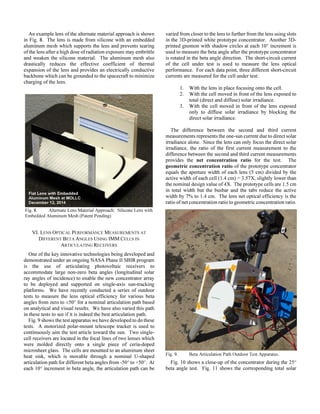
Fig. 1. New Baseline Concentrator Module.
Presented at the 43rd IEEE Photovoltaic Specialists Conference (PVSC), Portland, Oregon, June 2016
2. The photovoltaic receivers are mounted onto 25-micron
thick graphene sheet radiators for spreading and radiating the
waste heat from the photovoltaic cells.
The lenses are specially designed and optimized to focus
well despite large variations in beta angle, by employing a
small articulation of the receivers relative to the lens. Fig. 2
shows a 3D-printed model with simulated articulating
photovoltaic receivers properly positioned in the focal lines
produced by the glass-silicone lens for both zero and 50° beta
angles. Note that the focal lines are sharp for both conditions.
This 3D model will be used to fine-tune the articulation path to
maximize cell current and power. Note the slots to allow for
variation in receiver position relative to the nominal U-shaped
path.
III. 4-JUNCTION IMM CELLS AND RECEIVERS
The prismatic pattern of the new lens is optimized to provide
exceptional color-mixing to avoid chromatic aberration losses
in the 4-junction IMM cells used in the new concentrator
module. Fig. 3 shows one of the three-cell circuits produced
by SolAero for the new concentrator module. Each cell has a
length of 3.2 cm and a total width of 1.5 cm. The three cells
are wired in parallel with a single bypass diode protecting the
three-cell group. The cell string is slightly shorter than the 10
cm focal line produced by the lens. The tabbing and
interconnection scheme provides a robust assembly for ground
testing. Later flight units will be narrower and lighter. The 4-
junction IMM cells are supported on glass carriers beneath the
cells. We believe this program is the first to use 4-junction
IMM cells in a space concentrator application. Outstanding
performance is expected from the new concentrator module.
IV. GRAPHENE RADIATOR DEVELOPMENT
The 25-micron thick graphene sheet is not as robust as we
would prefer, so our team has been investigating ways of
strengthening the graphene sheet. One method is based on our
alternate lens strengthening approach of adding a mesh to the
silicone lens. Fig. 4 shows a small sample of graphene with an
aluminum mesh bonded to it. This approach is attractive.
Fig. 2. Glass-Silicone Lens Showing Focal Lines on Simulated
Articulating Photovoltaic Receivers at 0° and 50° Beta Angles (Patent
Pending).
Fig. 4. Graphene Sheet with Aluminum Mesh Bonded to Surface.
Fig. 3. SolAero 4-Junction IMM Cell Receiver Circuit.
3. As presented in our paper at the last PVSC, graphene sheet
offers a thermal conductivity to density ratio 10X better than
aluminum sheet, and 5X better than carbon-fiber-reinforced
sheet, and a 25-micron thickness is more than adequate for the
concentrator module size shown in Fig. 1. However, our team
was concerned about the emittance of the raw graphene, and
AFRL measured the infrared properties which confirmed a
relatively low 33% emittance, as shown in Fig. 5. We then
coated the graphene with a very thin layer of silicone and
AFRL confirmed much better infrared properties, yielding
more than double the emittance at 70%, as also shown in Fig. 5.
V. ALTERNATE LENS MATERIAL APPROACHES
While the glass-silicone lens is our baseline design, we are
also continuing to develop alternate lens material approaches
which require no glass. Our present favorite alternate approach
is a silicone lens with embedded aluminum mesh. Such a lens
will of course employ a UV-rejection coating on the sun-
exposed surface, as have our non-glass-superstrate lenses for
several successful flight experiments (including the silicone
mini-dome lenses on PASP+ in 1994-1995, the 4-year-exposed
MISSE UVR-coated silicone samples on ISS, the UVR-coated
stretched lens on TacSat 4), as well as many ground tests. To
further explore this option, we previously conducted high-
energy proton exposure testing at Auburn University at 5E12
p+/cm2
of 2.7 MeV protons, with no measurable change in
spectral transmittance. More recently, we conducted low-
energy proton exposure testing of the samples shown in Fig. 6.
Dr. Scott Messenger of SRM Consulting LLC tested these
samples at the Japan Atomic Energy Agency (JAEA), and they
held up well for 1E15 p+/cm2
of 30 keV protons, but suffered
some darkening for 10X higher fluence. The spectral
transmittance curves for the four samples were measured by
Dr. Dave Wilt at AFRL, with results shown in Fig. 7. These
samples were uncoated. We believe a thin UV-rejection
coating would greatly extend the radiation hardness of this lens
material approach. The mesh certainly strengthens the parts.
Fig. 5. Emittance of Silicone-Coated Graphene Sheet.
Fig. 6. Low-Energy Proton Exposed Samples.
Fig. 7. AFRL-Measured Spectral Transmittance of Samples.
4. An example lens of the alternate material approach is shown
in Fig. 8. The lens is made from silicone with an embedded
aluminum mesh which supports the lens and prevents tearing
of the lens after a high dose of radiation exposure may embrittle
and weaken the silicone material. The aluminum mesh also
drastically reduces the effective coefficient of thermal
expansion of the lens and provides an electrically conductive
backbone which can be grounded to the spacecraft to minimize
charging of the lens.
VI. LENS OPTICAL PERFORMANCE MEASUREMENTS AT
DIFFERENT BETA ANGLES USING IMM CELLS IN
ARTICULATING RECEIVERS
One of the key innovative technologies being developed and
demonstrated under an ongoing NASA Phase II SBIR program
is the use of articulating photovoltaic receivers to
accommodate large non-zero beta angles (longitudinal solar
ray angles of incidence) to enable the new concentrator array
to be deployed and supported on single-axis sun-tracking
platforms. We have recently conducted a series of outdoor
tests to measure the lens optical efficiency for various beta
angles from zero to ±50° for a nominal articulation path based
on analytical and visual results. We have also varied this path
in these tests to see if it is indeed the best articulation path.
Fig. 9 shows the test apparatus we have developed to do these
tests. A motorized polar-mount telescope tracker is used to
continuously aim the test article toward the sun. Two single-
cell receivers are located in the focal lines of two lenses which
were molded directly onto a single piece of ceria-doped
microsheet glass. The cells are mounted to an aluminum sheet
heat sink, which is movable through a nominal U-shaped
articulation path for different beta angles from -50° to +50°. At
each 10° increment in beta angle, the articulation path can be
varied from closer to the lens to further from the lens using slots
in the 3D-printed white prototype concentrator. Another 3D-
printed gnomon with shadow circles at each 10° increment is
used to measure the beta angle after the prototype concentrator
is rotated in the beta angle direction. The short-circuit current
of the cell under test is used to measure the lens optical
performance. For each data point, three different short-circuit
currents are measured for the cell under test:
1. With the lens in place focusing onto the cell.
2. With the cell moved in front of the lens exposed to
total (direct and diffuse) solar irradiance.
3. With the cell moved in front of the lens exposed
only to diffuse solar irradiance by blocking the
direct solar irradiance.
The difference between the second and third current
measurements represents the one-sun current due to direct solar
irradiance alone. Since the lens can only focus the direct solar
irradiance, the ratio of the first current measurement to the
difference between the second and third current measurements
provides the net concentration ratio for the test. The
geometric concentration ratio of the prototype concentrator
equals the aperture width of each lens (5 cm) divided by the
active width of each cell (1.4 cm) = 3.57X, slightly lower than
the nominal design value of 4X. The prototype cells are 1.5 cm
in total width but the busbar and the tabs reduce the active
width by 7% to 1.4 cm. The lens net optical efficiency is the
ratio of net concentration ratio to geometric concentration ratio.
Fig. 10 shows a close-up of the concentrator during the 25°
beta angle test. Fig. 11 shows the corresponding total solar
Fig. 8. Alternate Lens Material Approach: Silicone Lens with
Embedded Aluminum Mesh (Patent Pending)
Fig. 9. Beta Articulation Path Outdoor Test Apparatus.
5. irradiance one-sun test of the cell at 25° beta angle. Fig. 12
shows the concentrator test at 50° beta angle. The nominal U-
shaped path for receiver articulation is visible on the right side
of the prototype concentrator in Fig. 12, with a nylon threaded
rod and wingnuts securing the position. Slots to vary the
position from closer to the lens to further away from the lens
are also visible.
Fig. 13 shows the concentrator test for a zero beta angle. A
grid is visible in this photo on the inner wall of the
concentrator module. This grid is used to visually align the
photovoltaic cell plane to be parallel to the lens plane.
Fig. 14 shows the measured net lens optical efficiency versus
beta angle for the nominal receiver articulation path, and
compares the measured results to predicted results. Two
predicted curves are shown, the higher with zero
absorption/scattering loss and the lower with 2%
absorption/scattering loss (more realistic). The experimental
data are shown with ± 4% error bars, a rough estimate of the
probable error in these measurements. Note the greatly
expanded non-zero vertical axis in the graph. The predicted
and measured results show excellent agreement.
Fig. 15 shows the results of varying the articulation path for
50° beta angle. Note that the nominal path is best, which
measurements at other beta angles also confirmed.
Fig. 10. Concentrator Test at 25° Beta Angle.
Fig. 11. One-Sun Test at 25° Beta Angle. Fig. 13. Concentrator Test at Zero Beta Angle.
Fig. 12. Concentrator Test at 50° Beta Angle.
6. VII. UPDATED MASS AND PERFORMANCE METRICS
A refined areal mass density estimate for the three key
concentrator blanket elements is shown in Table 1. These key
elements are the lens, heavily shielded photovoltaic receiver
(150-micron equivalent coverglass front and back), and
graphene radiator. Later in the program we will also estimate
the remaining array mass elements for the complete solar array
wing, including the solar array deployment and support
platform being developed by DSS using their patented roll-out
solar array approach [4]. For the limited elements shown in
Table 1, the total areal mass density if about 0.43 kg/m2
.
As discussed above, SolAero has recently developed and
produced a pilot run of 4-junction IMM cells for the new
concentrator. The average one-sun efficiency (AM0 spectrum,
room temperature) of these cells was approximately 31% on a
total area basis, or 33% on an active area basis. With the
normal anticipated gain in performance at the 4X concentration
of the new concentrator, the average cell efficiency should be
about 35%. With the 92% lens efficiency from the tests
described above, the combined lens-cell efficiency should be
about 32%. While there will of course be additional loss
factors for the array, including cell operating temperature
effects, wiring and mismatch losses, etc., a target beginning-
of-life blanket efficiency value of 28% for higher earth orbits
is reasonable, yielding an areal power density of about
380 W/m2
. With the 0.43 kg/m2
areal mass value for the lens
plus heavily shielded photovoltaic receiver plus radiator
combination from Table 1, this yields approximately 900 W/kg
at the blanket level, a remarkable number.
Compared to a conventional one-sun space array, the new
concentrator uses about 75% less of the expensive IMM cell
area to produce each Watt of power in space. Since the
remaining concentrator blanket materials (glass, silicone,
graphene, etc.) are relatively reasonable in cost, a realistic
target cost for the new concentrator array is at least 50% lower
than for a one-sun array of the same power rating. Compared
to a conventional one-sun space array, the areal mass density
of the concentrator blanket is less than half the value for the
one-sun array, and the specific power at the blanket level is
more than double the value for the one-sun array.
ACKNOWLEDGEMENT
The work reported in this paper was made possible by a
NASA Phase II SBIR contract from NASA GRC to Mark
O’Neill, LLC. Our team is grateful to NASA for supporting
this work. We are also grateful to Dr. Scott Messenger of SRM
Consulting and Dr. Dave Wilt of the Air Force Research Lab
(AFRL) for their important contributions in radiation testing
and optical property measurements, respectively.
REFERENCES
[1] P. Jenkins et al., “Initial Results from the TacSat-4 Solar
Cell Experiment,” 39th IEEE PVSC, 2013.
[2] M. O’Neill et al., “Development of More Robust Stretched
Lens Array (SLA) Technology with Improved
Performance Metrics and Significantly Expanded
Applications,” 23rd Space Photovoltaic Research and
Technology (SPRAT) Conference, 2014.
[3] M. O’Neill et al., “Recent Space PV Concentrator
Advances: More Robust, Lighter, and Easier to Track,”
42nd IEEE PVSC, New Orleans, 2015.
[4] B. Spence et al., “Rollable and Accordion Foldable
Refractive Concentrator Space Solar Array Panel, U.S.
Patent 8,636,253, 2014.
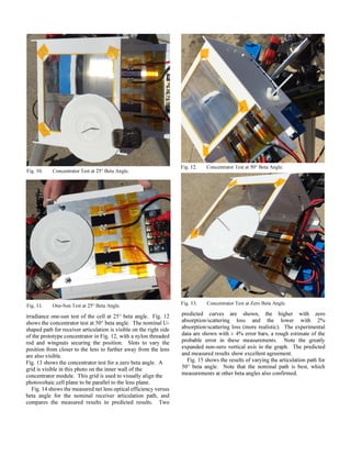
Fig. 14. Measured and Predicted Net Lens Optical Efficiency
Versus Beta Angle.
Fig. 15. Receiver Articulation Path Variation from Nominal at 50°
Beta Angle.
4.00 X 3.03 X
5.00 cm Cell Width 1.45 cm
Receiver
Width
1.65 cm
Major
Subsystem
Element
Element
Area per
sq.m.
Aperture
Thickness Density
Mass/
Aperture
Subtotals:
Mass/Aperture
(sq.m.) (cm) (g/cu.cm.) (kg/sq.m.) (kg/sq.m.)
Lens 50 micron CMG/50 micron Silicone 1.000 0.010 1.790 0.179 0.179
Radiator Silicone-Coated Graphene Radiator 1.000 0.005 1.420 0.071 0.071
CMG Microsheet Cover Glass 0.330 0.008 2.550 0.063
Cover Glass Adhesive 0.330 0.003 1.030 0.009
IMM Cell 0.330 0.001 5.300 0.017
Glass Carrier 0.330 0.008 2.550 0.063
Thermally Conductive Adhesive 0.330 0.005 1.500 0.025
0.427 kg/sq.m.
Aperture Width
Total Areal Mass Density:
Areal Mass Density for 4X Line-Focus SLA with Glass/Silicone Lens, Graphene Radiator
Sheet, and Photovoltaic Receiver Elements for IMM Cell with 150 micron (6 mil) Equivalent
Cover Glass Shielding Front and Back
Geometric Concentration Ratio Physical Concentration Ratio
Receiver 0.177
TABLE 1. AREAL MASS BREAKDOWN OF LENS + RECEIVER
+ RADIATOR.