1. Abstract When we say that an electric motor
is a device that transforms electric power into
mechanical power, we say two things. First, that
the motor is ?and behaves as ?a transformer.
Second, that it stands at the dividing line
between electrical and mechanical phenomena.
In the case of permanent magnet motors, this
power transformation works in both directions
so that the electrical impedance depends on the
mechanical load, while the mechanical behavior
of the motor depends on the conditions at the
electrical end. This being the case, it should be
possible to represent a motor ?s mechanical
load, on the electrical side, by a set of familiar
electrical components such as capacitors or
resistors.
Introduction
The metric system of units has undergone a
number of changes in its history, of which the
latest is the SI (Systeme International d’Unites).
This system has become popular in most of the
industrialized world, largely because it is a
coherent system, in which the product or
quotient of two or more units is the unit of the
resulting quantity. Certain simplifications result
from using this form of the metric system.
In the Sl system, force IS measured in Newtons
(N) and distance in meters (m). Consequently,
the units of torque are Nm (see Table 1.). If a
motor shaft rotates at an angular velocity of
ωM radians per second, with torque TM, the
mechanical power output will be equal to the
product TM, and ωM and the units will be watts
if TM is in Nm.
Motor manufacturers usually specify a torque
constant (KT) and a voltage constant (KV) for
their motors. These constants have different
values when the torque and speed are
measured in
English units, but they have the same numerical
value when Sl units are used. This becomes
obvious when you consider that the electrical
input power must be equal to the mechanical
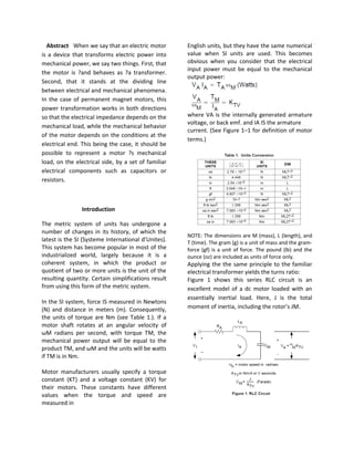
output power:
where VA is the internally generated armature
voltage, or back emf. and IA IS the armature
current. (See Figure 1–1 for definition of motor
terms.)
NOTE: The dimensions are M (mass), L (length), and
T (time). The gram (g) is a unit of mass and the gram-force
(gf) is a unit of force. The pound (lb) and the
ounce (oz) are included as units of force only.
Applying the the same principle to the familiar
electrical transformer yields the turns ratio:
Figure 1 shows this series RLC circuit is an
excellent model of a dc motor loaded with an
essentially inertial load. Here, J is the total
moment of inertia, including the rotor’s JM.
2. Thus, the non-dimensional turns ratio N1/N2 is
analogous to the dimensional torque (or
voltage) constant KTV. Furthermore, equations
(2) and (4) give us a clear hint that the angular
velocity (ωM) is analogous to voltage, while the
torque (TM) is analogous to current.
The units of Km may be either Nm/A. or
Vsec/rad. Thus, specifying both KT and KV for a
motor is like measuring and specifying both the
voltage ratio and the current ratio of a
transformer, and can only make sense where
redundancy is required.
LITERATURE REVIEW
Power quality issues and remedies are relevant
research topics and a lot of advanced
researches are being carried out in this area.
These issues are mainly due to increased use of
power electronic devices, nonlinear loads and
unbalance in power systems. Dynamic loads
cause power quality problems usually by
voltage or current variations such as voltage
dips, fluctuations, momentary interruptions,
oscillatory transients, harmonics, harmonic
resonance etc.[2]. Various publications define
power quality in different aspects.
According to IEEE Recommended Practice for
Monitoring Power Quality (IEEE Std 1159-
1995), Power quality is defined as “concept of
powering and grounding sensitive equipment in
a manner that is suitable for operation of that
equipment.”
Power quality issues- Definitions
Definitions for power quality issues in power
systems with non sinusoidal waveforms and
unbalanced loads are detailed in [5-9]. The
definitions and terminology used in conjunction
with power quality are as follows:
Voltage quality can be interpreted as the quality
of voltage delivered by the utility to the
consumers and is concerned with the deviations
of the voltage from the ideal one. The ideal
voltage is a single frequency sine wave of
constant frequency and constant magnitude.
Current quality deals with the deviations of the
current from the ideal one which should be
sinusoidal wave current of constant frequency
and required magnitude and should also be in
phase with the supply voltage. Voltage quality
deals with what the utility delivers to the
customer and current quality deals with what
the customers take from the utility and are
mutually dependent.
Power quality is the combination of voltage
quality and current quality. Power quality is
concerned with deviations of voltage and/or
current from the ideal. 7 Voltage magnitude
variation is the increase or decrease in voltage
magnitude due to load variations, transformer
tap–changing, switching of capacitor banks or
reactors etc.
Voltage frequency variation is the variation in
frequency of supply voltage due to the
imbalance between load and generation units.
Current magnitude variation is the variation of
the load current magnitude which also results in
voltage magnitude variations.
Current phase variation – Ideally, the voltage
and current waveforms should be in phase so
that the power factor perceived by the source is
unity. Deviation from this situation is termed as
current phase variation.
Voltage and current imbalances – Voltage
imbalance in three phase systems where the
rms values of the voltages in each phase or the
phase angle differences between consecutive
phases are not equal, can affect the ratio of
negative sequence and positive sequence
voltage components. This can result in large
differences between the highest and lowest
values of voltage magnitude and phase
difference. The voltage imbalance leads to large
load current imbalances.
Voltage fluctuation –The fast variation in
voltage magnitude is called voltage fluctuation
or ‘voltage flicker’ and can affect the
performance of the equipment.
Harmonic voltage distortion – The ideal voltage
waveform is a sinusoidal wave of constant
frequency. But, when there is voltage
distortion, it may be a sum of sine waves with
frequencies which are multiples of fundamental
frequency. These non-fundamental components
3. contribute to harmonic distortion. The
harmonic current components result in
harmonic voltage components and hence a
non-sinusoidal voltage in the system.
Harmonic current distortion – Harmonic current
distortion is the complementary phenomenon
of harmonic voltage distortion. They are
mutually dependent as harmonic voltage
distortion is mainly due to non-sinusoidal load
currents.
Inter-harmonic voltage and current components
are generated by equipment such as cyclo-converters,
heating controllers and arc
furnaces, which generate current components
at such frequencies which are not integral
multiples of fundamental frequency. In fact,
there may be sub-harmonic frequency currents
as well. These inter-harmonic components can
cause resonance between the line inductances
and capacitor banks. The sub-harmonic currents
can lead to saturation of transformers and in
turn to damage of synchronous generators and
turbines.
Voltage notching - In three phase converters
during commutation from one device to
another, short circuits for short durations can
cause voltage reduction or notching. Voltage
notching leads to higher order harmonics.
Interruptions – Supply interruption is a
condition in which the voltage at the supply
terminals is close to zero or less than 10%
according to IEEE Standard 1159 -1995. Faults
or protection equipment mal-tripping can cause
interruptions.
Under voltages –Short duration under voltages
are known as voltage sags and longer duration
under voltages are called under voltages.
Voltage sag is a reduction in the supply voltage
magnitude followed by a voltage recovery after
a short period of time. Voltage sags are mostly
caused by short circuit faults in the system and
by starting of large motors.
Over voltages- Over voltages of very short
duration and high magnitude are called
transient over voltages/voltage spikes/voltage
surges. Over voltages with duration between
one cycle and one minute are called voltage
swells or temporary power frequency over
voltages. Longer duration over voltages are
called over voltages. Over voltages are caused
by lightning strokes, switching operations,
sudden load reduction, single phase short
circuits and nonlinearities.
Electromagnetic compatibility (EMC) – EMC is
defined by IEC (International Electrotechnical
Commission) as the ability of a device,
equipment or system to function satisfactorily
in its electromagnetic environment without
introducing intolerable electromagnetic
disturbances to anything in that environment
.
Sources of power quality issues
The increasing cost of energy led to the
introduction of efficient adjustable speed drives
using static power converters in 1970’s. This
brought about a wide change in application of
utilisation equipment in industrial power
systems. To minimise the electrical energy
costs, which are made up of kVA demand and
kWh charges, users began to apply capacitors in
their system to lower the demand charges.
Wide usage of capacitor banks with static
power 9 converters introduced harmonic
resonance problems. The causes of these power
quality problems are generally complex and
difficult to detect. In earlier days, the main
sources of waveform distortion were electric
arc furnaces, fluorescent lamps, electrical
machines and transformers.
(i) Arc-furnace: In Arc furnace, the voltage-current
characteristics of electric arcs are highly
nonlinear. Following arc ignition, the voltage
decreases due to the short-circuit current,
which is limited only by the power system
impedance.
(ii) Fluorescent lamp: In a fluorescent lamp, the
voltage builds up in each half cycle till it emits
light. Its current is limited by the non-linear
reactive ballast and hence distorted.
4. (iii) Rotating machines: They also generate
harmonics because the windings are embedded
in slots which are not exactly sinusoidally
distributed and mmf becomes distorted.
Generally, harmonics produced by rotating
machines are considered negligible compared
to those produced by other sources. Also, large
generators are usually connected to power grid
through delta-connected transformers thus
blocking the flow of third harmonic current.
(iv) Power transformers: They use magnetic
materials that are operated often in the
nonlinear region for economic purposes
resulting in the distorted (mainly third
harmonics) transformer magnetizing current
even if the applied voltage is sinusoidal. Large
numbers of power electronic loads installed in
power systems, also generate harmonics. Major
sources are identified as Desktop computers,
TVs, Fax Machines, Copiers, Microwave ovens,
Electric vehicle battery chargers, Thyristor
converters, UPS, ASDs, Welding machines, Static
var compensators, Inverters, SMPS, Fluorescent
lighting etc. The switching or commutation of
power semiconductor devices generates
voltage or current transients that are
characterized by a spectrum of frequencies.
Static VAR compensators are balanced three-phase
devices that use thyristors to control the
conduction time of shunt capacitors or
inductors during each half cycle in order to
maintain a desired terminal voltage. It
generates non sinusoidal currents Harmonics is
considered to be a major power quality issue.
The generation of harmonic currents by typical
harmonic loads are illustrated in the following
subsection.
Typical harmonic generating loads Of the
several harmonic producing loads such as
transformers, arc furnaces, welding equipments
etc., for the purpose of this work, it is decided
to consider four types of widely used loads,
both steady state and dynamic, which will
introduce non sinusoidal currents in three
phase AC network. The major harmonic loads
considered in this work are:
(a) Three phase diode bridge rectifier
(b) Three phase thyristor converter
(c) DC motor drive and
(d) Induction motor drive
OPERATIONAL PRINCIPLES
The proposed converter is depicted in Fig. 1. It
is derived from a flyback converter whose two
transformers are connected in series input and
parallel output. The upper transformer T1 is
used for delivering energy stored in the dc link
capacitor C1 to the output. The lower
transformer T2 delivers the input energy
directly to the output, as well as dc-link energy,
and has an additional function to limit the
current charging into the link capacitor by
controlling the input-current dead zone.
Accordingly, the proposed converter shows
different operations depending on the input-current
flow that is influenced by the voltage
applied to the anode of D2. Fig. 2 depicts a
powerflow diagram of the proposed converter.
The power flow is controlled by the imaginary
switch S, which is on or off based on the
relationship between the rectified line voltage
Vg and the link voltage VC1 scaled by k. k is a
constant value between 0 and 1 that is
determined by the primary inductances of the
two transformers. If Vg is greater than kVC1,
the switch S is on, and the input power is
supplied to the link capacitor and output stage.
In the opposite case, power transmission from
the ac line is stopped, and the output power is
supplied only by the link capacitor. Because the
decision of the switching point of S varies
according to the link capacitor voltage level, the
charge current of the link capacitor can be
further reduced as the link capacitor voltage is
increased. It follows that an excessive
5. increase of the link voltage can be suppressed.
Fig. shows the simplified diagram of the
proposed converter when the main switch Q is
turned on. Assuming that the anode voltage of
D2 is lower than the cathode voltage, D2 is
blocked, and the anode voltage ofD2 can be
written as follows by applying Kirchhoff’s
voltage law (KVL) along C1, L2, and L3:
where L2 and L3 are primary inductances of T1
and T2, respectively. Therefore, the critical
rectified line voltage Vg,critical that determines
the diode state is defined as
Introducing N, the inductance ratio of L2 to L3,
(2) can be rewritten as
DCM condition is successfully satisfied by
selecting the inductance ratio of L2 to L3.
Because the main switch carries input inductor
current as well as load current, the current
stress is heavy in general. Accordingly, it is
important to choose a proper value to make the
current stress as low as possible. Referring to
this, the maximum current stress can be written
as follows:
where V3 is calculated from (10) with the peak
value of the minimum line voltage. Fig. 8 shows
the maximum current stress according to
calculated (L1,N) pairs satisfying DCM, which
shows that lower current stress can be obtained
by selecting N to be as small as possible.
Therefore, the (L1,N) = (43 μH, 1.6) pair is used
for the design, and the power factor is
predicted to be about 0.95 from (3), (4), and
Fig. shows the reset time plots of ID3 and ID4
divided
by (1 − Dmax)Ts according to the transformer
turns ratios of n1 and n2 from (23) and (24). In
this figure, the minimum transformer turns
ratios of T1 and T2 are found to be 7.8 and 7.4,
respectively, and n1 = 8 and n2 = 8 are used in
the prototype converter. With these design
parameters, the calculated maximum link
voltage is about 395 V, and the maximum
switch voltage stress is calculated as 475 V. The
key component parameters used in the
prototype.
Experimental Results
A three-level AC–DC converter is proposed.
The proposed converter integrates the
operation of the boost power factor correction
and the three-level AC–DC Converter. There is
only a single stage power factor correction
converter; it is operated with two independent
controllers. One controller is used to perform
PFC and regulate the voltage across the primary
side DC-bus capacitors. The other controller is
used to regulate the output voltage, by sending
appropriate gating signals.
6. Fig, integrates an AC–DC boost PFC converter
into a three-level DC–DC converter. The AC–DC
boost section consists of an input diode bridge,
boost inductor Lin, boost diode Dx1, and switch
S4, which is shared by the multilevel DC–DC
section.
When S4 is off, it means that no more energy
can be captured by the boost inductor. In this
case, diode Dx2 prevents input current from
flowing to the midpoint of capacitors C1 and C2
and diode Dx1
Conducts and helps to transfer the energy
stored in the boost inductor Lin to the DC bus
capacitor. Diode Dx3 bypasses Dx2 and makes a
path for circulating current.
Although there is only a single
converter, it is operated with two independent
controllers. One controller is used to perform
PFC and regulate the voltage across the primary
side DC-bus capacitors by sending appropriate
gating signals to S4. The other controller is used
to regulate the output voltage by sending
appropriate gating signals to S1 to S4. It should
be noted that the control of the input section is
decoupled from the control of the DC–DC
section and thus can be designed separately.
The gating signal of S1, however, is dependent
on that of S4, which is the output of the input
controller; how this signal is generated is
discussed in detail later in this project.
The gating signals for S2 and S3 are
easier to generate as both switches are each ON
for half a switching cycle, but are never ON at
the same time. Typical converter waveforms are
shown in Fig
1) Reduced cost compared to two-stage
converters: Although the proposed converter
may seem expensive, the reality is that it can be
cheaper than a conventional two-stage
converter. This is because replacing a switch
and its associated gate drive circuitry with four
diodes reduces cost considerably even though
the component count seems to be increased
this is especially true if the diodes are ordered
in bulk numbers.
2) Better performance than a single-stage
converter: The proposed single-stage converter
can operate with a better input power factor for
universal input line applications than a single-controller,
single-stage because it does have a
dedicated controller for its input section that
can perform PFC and regulate the DC-bus
voltage. The presence of a second controller
also allows the converter to operate with better
7. efficiency and with less output ripple as each
section of the converter can be made to
operate in an optimal manner.
3) Improved light-load efficiency: The proposed
converter can be designed so that it has a
conventional DC-bus voltage of 400 V. Since the
converter is a multilevel converter, a 400 V DC
bus means that each switch will be exposed to a
maximum voltage of 200 V. Having 200 V across
a MOSFET device instead of 400 V (as is the case
with two-level converters) results in a 75%
reduction in turn on losses when the converter
is operating under light-load conditions and
there is an insufficient amount to current
available to discharge the switch output
capacitances before the switches are turned on.
4) Increased design flexibility: Since the
converter is a multilevel converter, it can be
operated with high dc-bus voltage (800 V),
standard dc-bus voltage (400 V), or any dc-bus
voltage 400 V < Vbus <800 V. There are
advantages to operating with high dc-bus
voltage or with standard dcbus voltage. The fact
there is flexibility in the level that the dc-bus
voltage is set means that there is considerable
flexibility in the design of the converter.
CONCLUSION
In this paper a review of position control
methods for the fundamentals of various
techniques have been introduced, mainly back-
EMF schemes and estimators, as a useful
reference for preliminary investigation of
conventional methods. Advances in the position
control and applications were also discussed. To
provide insight in control techniques and their
benefits a classification of existing methods and
newer methods were presented with their
merits and drawbacks. From the above
discussion, it is obvious that the control for
BLDC motors using position sensors, such as
shaft encoders, resolvers or Hall-effect probes,
can be improved by means of the elimination of
these sensors to further reduce cost and
increase reliability. Furthermore, sensorless
control is the only choice for some applications
where those sensors cannot function reliably
due to harsh environmental conditions and a
higher performance is required.As a result be
believe that designing applications with our
motors is simpler and less risky.
References
[1] Jun-Young Lee, Student Member, IEEE
“Single-Stage AC/DC Converter With Input-
Current Dead-Zone Control for Wide Input
Voltage Ranges”IEEE Transactions On Industrial
Electronics, Vol. 54, No. 2, April 2007.
[2]Wu Chen, Student Member, IEEE, and Xinbo
Ruan, Senior Member, IEEE Zero-Voltage-
Switching PWM Hybrid Full-Bridge “Three-Level
Converter With Secondary-Voltage Clamping
Scheme”IEEE Trans On Industrial Electronic, Vol.
55, No. 2, February 2008.
[3]J. Marcos Alonsor. IEEE, Marco A. Dalla
Costa, Student Member, IEEE, and Carlos Ordiz
“Integrated Buck-Flyback Converter as High-
Power-Factor Off-Line Power Supply” IEEE
Trans. On Industrial Electron, Vol. 55, No. 3,
March 2008.
[4] H. S. Athab and D. D.-C. Lu, “A high-efficiency
ac/dc converter with quasi-active
power factor correction,” IEEE Trans. Power
Electron., vol. 25, no. 5, p. 1103-1109, May
2010.
[5] J. M. Kwon, W. Y. Choi, and B. H. Kwon,
“Single-stage quasi-resonant flyback converter
for a cost-effective PDP sustain power module,”
IEEETrans. Ind. Electron., vol. 58, no. 6, pp.
2372–2377, Jun. 2011.
[6] Jindong Zhang, Member, IEEE, Fred C. Lee,
Fellow, IEEE, and Milan M. Jovanovic´, Fellow,
IEEE “An Improved CCM Single-Stage PFC
Converter With a Low Frequency Auxiliary
Switch” IEEE Transactions On Power Electronics,
Vol. 18, No. 1, January 2003.
[7] H. Athab and D. Lu, “A single-switch ac/dc
flyback converter using a CCM/DCM quasi-active
power factor correction front-end,” IEEE
Trans.Ind. Electron., vol. 59, no. 3, pp. 1517–
1526, Mar. 2012.
[8] N. Golbon and G. Moschopoulos, “A low-power
ac–dc single-stage converter with
reduced dc bus voltage variation,” IEEE Trans.
8. Power Electron., vol. 27, no. 8, pp. 3714–3724,
Jan. 2012.
[9] P. K. Jain, J. R. Espinoza, and N. Ismail, “A
single-stage zero-voltage zero-current-switched
full-bridge DC power supply with extended load
power range,” IEEE Trans. Ind. Electron., vol. 46,
no. 2, pp. 261–270, Apr. 1999.
[10] G. Moschopoulos, “A simple AC–DC PWM
full-bridge converter with integrated power-factor
correction,” IEEE Trans. Ind. Electron.,
vol. 50, no. 6, pp. 1290–1297, Dec. 2003.
[11] G. Moschopoulos, Q. Mei, H. Pinheiro, and
P. Jain, “PWM full-bridge converter with natural
input power factor correction,” IEEE Trans.
Aerospace.Electron. Syst., vol. 39, no. 2, pp.
660–674, Apr. 2003.
[12] P. Das, S. Li, and G. Moschopoulos, “An
improved AC–DC single-stage full-bridge
converter with reduced DC bus voltage,” IEEE
Trans. Ind.Electron., vol. 56, no. 12, pp. 4882–
4893, Dec. 2009.
[13] Praveen K. Jain, Senior Member, IEEE, Jos´e
R. Espinoza, Member, IEEE, and Nasser A. Ismail
“A Single-Stage Zero-Voltage Zero-Current-
Switched Full-Bridge DC Power Supply with
Extended Load Power Range” IEEE Transactions
On Industrial Electronics, Vol. 46, No. 2, April
1999
[14] Javier Sebastián, Member, IEEE, Arturo
Fernández, Member, IEEE, Pedro Jose Villegas,
Member, IEEE, Marta Maria Hernando,
Member, IEEE, and Miguel J. Prieto, Member,
IEEE “New Active Input Current Shapers to
Allow AC-to-DC Converters with Asymmetrically
Driven Transformers” to Comply With the IEC-
1000-3-2 IEEE Transactions On Power
Electronics, Vol. 17, No. 4, July 2002.
[15] Qun Zhao, Student Member, IEEE, Fred C.
Lee, Fellow, IEEE, and Fu-sheng Tsai, Member,
IEEE Voltage and Current Stress Reduction in
“Single-Stage Power Factor Correction AC/DC
Converters With Bulk Capacitor Voltage
Feedback” IEEE Transactions On Power
Electronics, Vol. 17, No. 4, July 2002

![Thus, the non-dimensional turns ratio N1/N2 is
analogous to the dimensional torque (or
voltage) constant KTV. Furthermore, equations
(2) and (4) give us a clear hint that the angular
velocity (ωM) is analogous to voltage, while the
torque (TM) is analogous to current.
The units of Km may be either Nm/A. or
Vsec/rad. Thus, specifying both KT and KV for a
motor is like measuring and specifying both the
voltage ratio and the current ratio of a
transformer, and can only make sense where
redundancy is required.
LITERATURE REVIEW
Power quality issues and remedies are relevant
research topics and a lot of advanced
researches are being carried out in this area.
These issues are mainly due to increased use of
power electronic devices, nonlinear loads and
unbalance in power systems. Dynamic loads
cause power quality problems usually by
voltage or current variations such as voltage
dips, fluctuations, momentary interruptions,
oscillatory transients, harmonics, harmonic
resonance etc.[2]. Various publications define
power quality in different aspects.
According to IEEE Recommended Practice for
Monitoring Power Quality (IEEE Std 1159-
1995), Power quality is defined as “concept of
powering and grounding sensitive equipment in
a manner that is suitable for operation of that
equipment.”
Power quality issues- Definitions
Definitions for power quality issues in power
systems with non sinusoidal waveforms and
unbalanced loads are detailed in [5-9]. The
definitions and terminology used in conjunction
with power quality are as follows:
Voltage quality can be interpreted as the quality
of voltage delivered by the utility to the
consumers and is concerned with the deviations
of the voltage from the ideal one. The ideal
voltage is a single frequency sine wave of
constant frequency and constant magnitude.
Current quality deals with the deviations of the
current from the ideal one which should be
sinusoidal wave current of constant frequency
and required magnitude and should also be in
phase with the supply voltage. Voltage quality
deals with what the utility delivers to the
customer and current quality deals with what
the customers take from the utility and are
mutually dependent.
Power quality is the combination of voltage
quality and current quality. Power quality is
concerned with deviations of voltage and/or
current from the ideal. 7 Voltage magnitude
variation is the increase or decrease in voltage
magnitude due to load variations, transformer
tap–changing, switching of capacitor banks or
reactors etc.
Voltage frequency variation is the variation in
frequency of supply voltage due to the
imbalance between load and generation units.
Current magnitude variation is the variation of
the load current magnitude which also results in
voltage magnitude variations.
Current phase variation – Ideally, the voltage
and current waveforms should be in phase so
that the power factor perceived by the source is
unity. Deviation from this situation is termed as
current phase variation.
Voltage and current imbalances – Voltage
imbalance in three phase systems where the
rms values of the voltages in each phase or the
phase angle differences between consecutive
phases are not equal, can affect the ratio of
negative sequence and positive sequence
voltage components. This can result in large
differences between the highest and lowest
values of voltage magnitude and phase
difference. The voltage imbalance leads to large
load current imbalances.
Voltage fluctuation –The fast variation in
voltage magnitude is called voltage fluctuation
or ‘voltage flicker’ and can affect the
performance of the equipment.
Harmonic voltage distortion – The ideal voltage
waveform is a sinusoidal wave of constant
frequency. But, when there is voltage
distortion, it may be a sum of sine waves with
frequencies which are multiples of fundamental
frequency. These non-fundamental components](data:image/gif;base64,R0lGODlhAQABAIAAAAAAAP///yH5BAEAAAAALAAAAAABAAEAAAIBRAA7)