SlideShare a Scribd company logo
1 of 71
Download to read offline
Chapter 1: Semiconductor Theory
1.1 ATOM –Structure
Usually protons and electrons will be equal in number .Therefore, atoms are normally neutral,
electrically.
o If an atom loses an electron, it means that it has lost some -ve charge & hence has a net + ve
charge ……….. and vice versa.
1.1.1 Holes & Electrons (Silicon & Germanium)
Pls recall,
1. Electrons can occupy only some fixed orbits, called shells.
2. Each shell can be occupied by only some specific number of electrons.
3. The outer most shell called valence shell, may be only partially filled by electrons.
4. Figure 1.2 gives a 2 D simplified orbital arrangement of silicon & germanium atom.
5. Absence of an electron in a shell, is defined as a hole.
6. Silicon & Germanium atoms are electrically neutral (outer shell has 4 holes & 4
electrons each)
1
Fig 1.1 Atom - Structure
o Atom consists of a nucleus. Electrons in several
orbits move around the nucleus..
o Contains three basic Particles –Protons, Neutrons
& electrons.
o Nucleus contains two types of particles
o Protons : Positively charged particles.
o Neutrons : Particles with neutral charge.
o Electrons: Negatively charged particles (Charge =
1.602X 10⁻⁹
Coulombs).
Fig 1.2
1.2 Electron &Hole Dynamics
1.3 N type & P type Semiconductors
1,3,1 Intrinsic semiconductor: It is very pure chemically. It has equal numbers of electrons (-ve)
and holes (+ve). It has poor conductivity.
1,3,2 Extrinsic semiconductor:
o When a small amount, of impurity is added to a pure semiconductor, the conductivity of the
semiconductor is increased manifold.
o Such materials are known as extrinsic semiconductors.
o The deliberate addition of a desirable impurity, is called doping.
o Doping yields two types of semiconductors viz p type and n type.
o The impurity atoms are called dopants.
o Such a material is also called a doped semiconductor.
o Silicon & Germanium are the standard semiconductor atoms, used by the industry.
Some of the popular dopants used, in doping the tetravalent Si or Ge are,
Trivalent atoms such as Boron or Aluminium, for producing p type semiconductors.
Pentavalent atoms such as Arsenic or Phosphorous, for producing n type semiconductors.
n type: Refer fig 1.4. Pentavalent (5) impurities like Arsenic (As), Antimony (Sb), Phosphorous (P),
when added to either silicon or germanium, will produce N type semiconductors. Electrons are the
majority carriers.
p type: Refer fig 1.5. Trivalent (3) impurities like Indium (In), Boron (B), Aluminium (Al) when
added to either Silicon or Germanium, will produce P type semiconductors. Holes are the
majority carriers.
2
Refer fig 1.3.
o Electrons are –vely charged particles.
Electrons are repelled by –ve voltage.
Therefore, they will move towards a
terminal where + ve voltage is
applied.
o Holes are +vely charged particles.
Holes are repelled by + ve voltage. They
will move towards a terminal where -ve
Voltage is applied.
o Please note the direction of the current
flow is always opposite to the direction
of electron flow.
Fig 1.3
Fig 1.4 n-type pentavalent atom
Fig 1.5 p-type trivalent atom
1.4 pn junction
Figure 1.6 shows independent p type independent n type semi-conductor.
Fig 1.6 Semiconductor material n-type and p-type
o Majority carriers of n type are electrons.
o Majority carriers of p type are holes.
1.4.1 Diffusion
Refer fig 1.7. Due to thermal agitation, electrons and holes start moving randomly, even if there is
no bias. Look at the diffusion process below.
Few electrons close to the junction, start
crossing the junction, to reach p side
Few holes close to the junction, start
crossing the junction, to reach the n side
These electrons combine with some holes
in the p side, to create some –ve ions.
These holes combine with electrons in the
n side to create some +ve ions.
Due to these ions, a -ve voltage build up
(barrier) is created, on the p side.
Due to these ions, a +ve voltage build up
(barrier) is created on the n side.
3
Majority and minority carriers
Majority carriers:
o The more abundant charge
carriers
o Primarily responsible for
current transport in a
semiconductor.
o n-type semiconductors:
Electrons
o p-type semiconductors: Holes.
Minority Carriers:
o The less abundant charge
carriers
o n-type semiconductors: Holes
o p-type semiconductors:
Electrons.
Fig 1.7 shows a p type and n
type conductor joined together
(fabricated) to form a p-n
junction
o There is no external voltage
(bias) applied.
o Initially, pn junction is
electrically neutral.
Fig 1.7 p-n junction diode – No bias voltage
This barrier voltage build up is shown in the figure 1.8.
Fig 1.8 Barrier Voltage at p-n junction
1.4.2 Depletion region
o In the diffusion process mentioned above, when the barrier potential is reached, further
diffusion stops.
o No charge carriers (electrons or holes) will be present, closer to the junction.
o Only ionized atoms (+ve and –ve), will be present on either side of the junction.
o This region is known as depletion region.
1.5 pn junction biasing
1.5.1 Reverse biased p-n junction
Refer figure 1.9.
What is reverse bias?
An external dc voltage (bias) is applied to a diode such that, p side is connected to the –ve
terminal and n side is connected to the +ve terminal of a battery.
4
o Barrier voltage is typically 0.7 V, for Silicon.
o Barrier voltage is typically 0.3 V, for
Germanium.
o At around the barrier voltage, electrons
(from n side) are repelled by the – ve
barrier voltage in the p side.
o At around the barrier voltage, holes (from p
side) are repelled by the +ve barrier
voltage in the n side.
o Therefore further diffusion stops.
Fig 1.9 Reverse biased p-n junction
Result: Majority carriers cannot flow across junction and therefore, under reverse bias
conditions, no current flow is possible. In other words, forward current does not flow.
1.5.2 Forward biased p-n junction
Refer figure 1.10.
What is forward bias?
An external dc voltage (bias) is applied to a diode such that n side is connected to the –ve
terminal and p side is connected to the +ve terminal of a battery.
o This biasing arrangement decreases the barrier voltage, as shown in the figure 1.10.
o Barrier voltage at n, becomes less +ve and the barrier voltage at p becomes less –ve.
o Electrons (majority carriers) in the n side, are attracted across the junction, towards the p
side and are attracted towards the +ve terminal.
o Holes (majority carriers) in the p side, are attracted across the junction, towards the n side
and are attracted towards the –ve terminal.
Fig 1.10 Forward biased p-n junction
5
o This biasing arrangement increases the
barrier voltage, as shown in the figure.
o Barrier voltage at n, becomes more +ve
and the barrier voltage at p becomes
more –ve.
o Electrons (majority carriers) in the n
side, are repelled away from the junction
and are attracted towards the +ve
terminal.
o Holes (majority carriers) in the p side,
are repelled away from the junction, and
are attracted towards the –ve terminal.
o Consequently, depletion region further
widens and barrier voltage increases as
shown.
o Consequently, depletion
region decreases and the
barrier voltage also
reduces, as shown.
Result: Majority carriers will
flow across junction and
therefore, under positive
bias conditions, current flow
is possible. In other words,
forward current is flows.
Chapter 2: Semiconductor Diodes and Applications
Syllabus: Semiconductor Diodes and Applications (Text-1) : p-n junction diode, Characteristics
and Parameters, Diode approximations, DC load line analysis, Half-wave rectifier, Two-diode Full-
wave rectifier, Bridge rectifier, Capacitor filter circuit, Zener diode voltage regulators: Regulator
circuit with no load, Loaded Regulator, Series and Shunt diode Clipping Circuits, Clamping Circuits:
Negative and Positive Clamping Circuits, Numerical examples as applicable.
2.1 p-n junction diode
What is a diode?
Fig 2.1 Semiconductor diode with leads
Draw the circuit symbol and indicate current flow.
Fig 2.2
Fig 2.3
Diode size Cathode
Identification
Forward current
(mA)
Reverse voltage
(V)
Small- Color band or dot 100 75
Medium Diode Symbol 400 200
Large Threaded portion Few amperes Few hundreds
6
Refer fig 2.1 and 2.2
o It is a semiconductor device with
a p-n Junction.
o It is a one way device.
o Allows current to flow when
forward biased (p: + ve and n:
-ve).
o Almost totally blocks current flow
when reverse biased (p: - ve and
n: +ve).
o Therefore, a diode is a 2 terminal
component.
o It has two electrodes called
anode and cathode.
o Anode is attached to p side and
cathode to n side.
Diodes Power classification: Refer
fig 2.3.
o Low power diodes: Usually
small diodes can handle low
currents up to 100mA. Power
dissipation will be less than 800
milli-watts.
o High power diodes: Large
diodes can handle high currents
(1 to 10 Amperes). Power
dissipation will be less than 1
watt to 10 watts.
o Look at the table below
2.2 Characteristics and parameters:
2.2.1 Diode characteristics: Refer fig 2.4 and 2.5
Fig 2.4
2.2.2 Forward characteristics (Silicon): Refer fig 2.5
Up to 0.7 V
o As the forward bias is increased from 0.1 to 0.7 V, the diode hardly conducts the forward
current is very low (less than 100 mA).
Fig 2.5 Silicon diode – Fwd and Rev characteristics
2.2.3 Reverse characteristics (Silicon)
0 to -50 V
o Please note the change of scale, in the y axis between forward & reverse characteristics.
7
o It is the study of, ‘voltage-
across-the-diode’ versus
‘current- through-the-diode’.
o As we know, diode is a p-n
junction semi-conductor device.
o When it is forward biased,
diode characteristics is a study
of forward voltage VF &
forward current IF.
o When it is reverse biased, the
diode characteristics is a study
of reverse voltage VR &
reverse current IR.
Beyond 0.7 V
o As the forward bias is
increased beyond 0.7
V, the forward current
increases very
sharply.
o Increasing the forward
bias beyond say 1.0
V, will destroy a
diode due to
excessive forward
current.
o A current limiting
resistor is needed in
the circuit to protect
the diode.
o Reverse current IR, is often very low (not more than 1 μA) for reverse voltages up to -75 V for
silicon
o IR is negligible compared to IF.
o For all practical purposes the diode behaves like an open circuit.
Beyond -75 V:
o Reverse break down happens (we shall study this later).
o The current increases abruptly.
o This can destroy the diode, unless protected by a current limiting resistor
2.2.4 Diode characteristics (germanium)
Fig 2.6 Germanium diode – Fwd and Rev characteristics
2.5 Forward & Reverse resistance : Refer fig 2.7
Fig 2.7
Problem 2.2: In fig 2.5 fig XXX calculate the reverse resistance of the silicon diode at VR =20V.
At VR = 20 V, IR = 90 nA (approx)
Therefore, reverse resistance (RR) =
V R
I R
=
20V
90nA
= 222 Mega ohms (approx)
2.2.6 Some of the important diode parameters.
8
Refer fig 2.6.
o The characteristics are
similar to that of silicon
diode.
o Forward voltage is 0.3 V
instead of 0.7 V.
o Reverse break down
voltage is -50 V instead of
-75 V.
o Reverse current is -1.0 μA
instead of -100 nA.
Problem 2.1: In fig 2.6, calculate
the forward resistance of the
germanium diode, at IF= 60mA
At IF = 60 mA, VF = 0.33 V
(approx)
Therefore, forward resistance
(RF) =
V F
I F
=
0.33V
60mA
= 5.5 ohms.
VF - Forward voltage drop (0.3 V for Ge and 0.7 V for silicon).
IF - Forward current .
VR - Reverse voltage.
rd - Dynamic resistance =
ΔV F
ΔI F
VBR - Break down voltage {50 V for Ge and 75 V for Si).
PD - Power dissipation.
2.2.7 Dynamic resistance rd
Recall the forward resistance that was calculated in example 2.1. RF =
V F
I F
. This is the DC
resistance of the diode, at one particular value of forward current. When the input varies by ∆VF,
there will be large variation, in forward current (∆IF). This is shown in fig 2.5
Dynamic resistance rd =
ΔV F
ΔIF
. rd is also known as ac resistance or incremental resistance
There is another way of calculating dynamic resistance. It is not discussed here since it is beyond
the scope of this book.The formula is rd =
26 mV
IF
Problem 2.3: What is the dynamic resistance of a diode with a forward current of 5 mA
rd =
26 mV
5mA
= 5.2 Ω.
Problem 2.4: For the dynamic characteristic shown in fig 2.8, determine the dynamic resistance at
40 mA.
Fig 2.8
2.3 Diode approximations:
2.3.1 Ideal Diode:
In the forward bias condition
It will have no forward resistance and will not drop any voltage across it. RF = 0 Ω and VF = 0 V.
Refer fig 2.9 a
In the reverse bias condition, an ideal diode will never have any reverse current, no matter
what the reverse voltage is. VR = ∞, IR = 0
9
IF = 40 mA.
Therefore, take a small interval around
40 mA as ∆IF, say from 20 mA to 60 mA.
∆VF for this range = 0.726 V - 0.71 V =
0.016 V
∆IF for this range = 60 mA - 20 mA =
40 mA
rd =
ΔV F
ΔI F
, =
0.016V
16mV
=
0.4 Ω
Therefore, what is an ideal diode?
1. Fwd Resistance = 0 Ohm
2. Fwd Voltage drop = 0 V
3. Rev resistance = Infinity
4. Rev current = 0 amp
Refer fig 2.9 b and 2.9 c
However, in practice, it is different as seen already in figures 2.5 and 2.6.
(a) (b) (c)
Fig 2.9 Diode Characteristics
What are the assumptions of a near ideal diode (Si)?
Fwd Voltage drop = constant
Rev current = negligible (can be ignored)
2.3.2 Practical diode
What is a practical diode (Si)?
Fwd Resistance = 0 to 20 Ohms
Fwd Voltage drop = 0.6 to 1.0 Volt
Rev current = few micro amps
2.3.3 Piece-wise approximation of a diode
The smooth diode curve of fig 2.5 or 2.6 can be approximated by taking samples at very close
intervals and interconnecting adjacent samples through short straight lines.
Problem 2.5: Construct a piece wise linear characteristics of a germanium diode, given that its
dynamic resistance is 0.6 Ω and forward current is 100 mA .
Look at fig 2.10
10
Fig 2.10
Join A B. The piece wise linear characteristic is the thick line segment shown.
2.3.4 DC equivalent circuits of a diode
Fig 2.11
Some equivalent circuits of diodes are shown in fig 2.11 and 2.12. Eqvt circuit of an ideal diode is
shown in Fig 2.12 (a) . In fig 2.12 (b) a practical diode with specific voltage drop VF =0.7 V (Si) or
0.3 V (Ge) is shown. Has a constant VF and negligible DC resistance (Zero)
(a) (c)
(b)
Fig 2.12 Diode Equivalent circuits
In fig 2.11(c), a more complete equivalent circuit, with a specific VF and a specific rd is shown. rd
represents the VF part.
Fig 2.13
Ideal diode. VF = 0.7 V (Silicon, by default), IF = 10 mA (given)
11
It is a Ge diode. VF = 0.3 V
Mark Point A = (0.3 V, 0 mA)
How to find B?
∆IF = 100 mA – 0 mA = 100 mA
∆VF = ∆IF X rd
= 100 mA X 0.6 Ω = 60 mV.
= 0.06 V
Point B = {(0.3 V + 0.06 V), 100 mA)}
= {(0.36 V, 100 mA)}
What is an equivalent circuit?
The electrical behaviour of the given circuit is accurately modelled
using a combination of, simple electrical components such as Resistor
(R), Inductor (L) and Capacitor (C).
Why equivalent circuit?
Equivalent circuit simplifies analysis of a complex circuit.
Problem 2.6: For the fig 2.13, what will be the drop across the
silicon diode, if IF = I0 mA and dynamic resistance is 0.8 Ω.
Drop across rd = IF X r d = 10 mA X0.8 Ω = 8 mV.
Total drop across the diode = 0.7 V + 8 mV. = 0.708 V.
Problem 2.7: In the circuit shown in fig 2.14, calculate IF . (Unless otherwise mentioned, the
diode is silicon by default.
E = IF.R + VF
10 V = (IF X 2.2K) + 0.7 V
 IF =
10V −0.7V
2.2K
= 4.22 mA.
Problem 2.8: For the same circuit in fig 2.14, what is the new IF if the diode has a dynamic
resistance of 0.3 Ω and R = 5 Ω .
The circuit is redrawn in fig 2.15.
E = IF.R + IF.rd + VF
10 V = (IF X 5 Ω) + (IF X 0.3 Ω) + 0.7 V
I F =
E−V F
R+rd
=
10V –0.7V
5 Ω+0.3Ω
= 9.3 V / 5.3 Ω = 1.76 A
Fig 2.14 Fig 2.15
2.4 D C load line analysis (Diodes)
This topic mainly revolves around three subtopics
a) DC Load line
b) Diode V-I Characteristics
c) Q point.
2.4.1 How to draw a DC Load line? Refer fig 2.16
As per Kirchoff’s Law,
E ▬ (IF X RL) ▬ VF = 0
E ▬ VF = IF X RL
E
RL
▬
V F
RL
= IF
12
IF = VF (−1
RL
) +
E
RL
Fig 2.16
E
RL
for a given circuit, is a constant.(say C)
IF = VF
(−1
RL
) + C
This is of the form y = mx + c (Straight line equation).where slope m = ▬
1
RL
The variables are the DC conditions, IF and VF. Hence the name, DC load line.
Problem 2.9: Let us draw a DC load line for the ckt in fig 2.16 where E = 6 V and RL = 150 Ω
E = (IF X RL) + VF
6 V = 150 IF + VF
( A) If IF = 0, Then VF = 6 V. For a diode,
VF = 6 V is of course absurd but a DC
load line does not take the device
characteristics into account
 Point A = (6 V, 0 mA)
( B) If VF = 0, Then IF =
6V
150 Ω
= 40 mA.
Point B =(0 V, 40 mA)
Draw a graph using the above values.
o A has coordinates VF = 6 V , IF = 0 mA.
o B has coordinates VF = 0 V , IF = 40 mA.
o Join AB as a Straight line.
o This is the load line.
o Note, slope of this load line = m = ▬
1
RL
2.4.2 Diode VI characteristics
This is the same curve in fig 2.5 and 2.6 Diode VI characteristic is the forward bias region (first
quadrant). This curve is super- imposed on the D C load line drawn above.
2.4.3 Q point (Quiescent point, DC bias point)
This is the point of intersection of DC load line and the diode V-I characteristics.
13
Fig 2.17
Problem 2.10: The Q point is (0.7
V , 35.3 mA). How?
For a silicon diode, VF = 0.7 V.
Recall from fig 2.16,
6 V = 150 IF + VF
6 V = 150 IF + 0.7 V
5.3 V = 150 IF
IF = 35.3 mA
 Q point is (0.7 V , 35.3 mA).
Problem 2.11: Find the load resistance for this circuit in fig 2.19, for IF = 20 mA
1) Draw Load line
VF = E- IF RL
a) For IF = 0, VF = E = 7.7 V.
 Plot A at (7.7 V , 0 mA)
b) Next, plot Q (Inter-section of diode
characteristics and IF = 20 mA line)
c) Join AQ and extend it to B. You will find B
intersecting Y axis at IF = 22 mA
Why? Let us find IF through circuit analysis
Problem 2.12: What is R L from the
load line?
We know that VF= E - IF RL
∆V F = 7.7 V - 0.7 V = 7.0 V.
∆I F = 20 mA – 0 mA = 20 mA.
RL =
ΔV F
ΔI F
=
7V
20mA
= 350 ohms
Using the equation VF = E – IF RL
When V F = 0, E = IF R L
7.7 V = IF X 350 Ω
I F = 7.7 V / 350 Ω = 22 mA.
14
Fig 2.18
For the given circuit this Q point is fixed
Conclusion:
(1) For a given VF and IF, the Q point is unique.
(2) VF for diodes is generally constant (0.7 V for Si
and 0.3V for Ge)
(3) Therefore, for altering the Q point IF should be
changed
(4) IF can be changed by either changing Input
voltage E or RL
Fig 2.19
Fig 2.20
2.4.4 Diode Parameters
1. IF (max) - Maximum forward DC current permissible
2. VF - Forward voltage drop (0.7 V for Si and 0.3 V for Ge)
3. VBR - Maximum reverse voltage that can be applied, beyond which break down occurs
4. rd - Dynamic resistance
5. IR - Reverse saturation current (current flow when diode is reverse biased )
6. Knee voltage - that forward voltage beyond which, forward current increases exponentially
7. P - continuous maximum power dissipation permissible at 25 deg C
2.5 Rectifiers
Define ‘’Rectifier’’
Rectifier is a device such as diode, that converts alternating current to direct current (ac to dc).
How is diode rectification done?
The rectification is done, by converting ac current to dc current, by suppression or
inversion of alternate half cycles.
2.5.1 Half wave rectifier (HWR):
Look at figure 2.21. A simple half wave rectifier is shown.
15
HWR Operation
Refer fig 2.21
o The input is fed through a transformer primary (terminals 1 and 2.).
o During +ve cycle of input, terminal 3 is +ve and terminal 4 is –ve.
o Diode gets forward biased and the current flow is clock wise, as shown in fig (a).
o Output voltage is IL RL.
o During – ve cycle of input # 4 is +ve and # 3 is –ve. Diode is reverse biased and diode
behaves like an open circuit, as shown. No current flows in the circuit.
o The output voltage is zero. The peak inverse voltage across diode is, the input voltage
(peak value).
o The Wave forms are shown in fig 2.21
Problem 2.13: For the circuit shown, determine the peak output voltage, peak load current and
diode peak inverse voltage. The ac input is 10V, the load resistance is 1 kΩ and the diode is
germanium.
16
Fig 2.21
Half-wave rectifier
Input voltage is 10 V rms.
Input peak voltage: Vp in = 2 X 10 V = 14.14 V
Output peak voltage: Vp out = Vp in - VF
= 14.14 - 0.3 V [Germanium]
= 13.84V
Peak inverse voltage = PIV = Vp in =14.14 V.
2.5.2 Full wave rectifier (FWR):
o As the name implies rectification happens, for both +ve and –ve cycles of the input wave.
Full wave rectifier, therefore, uses 2 diodes.
o A transformer input full wave rectifier (FWR) is shown in fig 2.23. The transformer becomes
complex, with a centre-tap operation.
FWR Center tap transformer:
Look at fig 2.23.
Fig 2.23 Center-tap transformer
FWR Operation:
A full wave rectifier using two diodes is shown in fig 2.24.
NOTE center tap is at ground (0V) potential.
Note, diode anodes are returned to ground through the load resistor RL
Input: + ve half cycle (Refer fig 2.25)
o Terminal 3 is +ve, with respect to ground (center tap) and D1 is forward biased.
17
Important : Unless otherwise mentioned, the
input is always specified as rms.
The relation between peak value & rms value is
Vrms = Vpeak / √2 and Irms = Ipeak / √2 and so on.
Fig 2.22
It consists of a primary winding (1,2) and two
secondary windings (3,4 and 5,6)
One end of, each of these secondary windings, is
joined together. In the figure 4 and 5 are joined.
The windings normally have the same number of
turns and therefore the 4, 5 junction becomes truly
a center tap.
The sense of these two secondary windings is in
such a way, that the two secondary outputs
always oppose each other, in phase.
o Terminal 6 is –ve, with respect to ground (center tap) and D2 is reverse biased.
o Current flows in the Dl loop as shown. (IL1)
o Resultant output (Vout1) is a +ve half cycle (Same phase as input).
Input: - ve half cycle (Refer fig 2.26)
o Terminal 6 is +ve, with respect to ground (center tap) and D2 is forward biased.
o Terminal 3 is –ve, with respect to ground (center tap) and D1 is reverse biased.
o Current flows in the D2 loop as shown. (IL2)
o Resultant output (Vout1) is a +ve half cycle (Inverted phase as input).
o The load current flows through RL in the same direction (right to left) whether the input is a +ve
half cycle or –ve half cycle. The wave forms are shown in the figure. The load current is, the
sum of the individual diode currents.
o Waveforms are shown in fig 2.27.
Fig 2.24 Full-wave rectifier Circuit (Two diodes)
18
2.5.2.3 Transformer related parameters
Let input voltage be Vp = Vpm sin wt.
Let wt =α
 Vp = Vpm sin α (primary)
Vs= Vsm sin α.
If the transformer has a turns ratio
Np : Ns, then
NS
NP
=
V SM
VPM
Fig 2.27 Full-wave rectifier waveforms
Transformer secondary resistance: The winding resistance Rs of transformer secondary, often
comes into play during current power calculations. .
Problem 2.14: If the transformer in the previous example is used, what is the peak secondary
current in this circuit in fig 2.28? Assume secondary has a resistance of 5 ohms.
Fig 2.28 Fig 2.29
Secondary peak voltage = 32.52 V. (previous example) . Refer equivalent circuit in fig 2.29.
Look at secondary equivalent circuit im =
V S
RS+Rf +RL
ipeak (secondary) =
32.52V
5 Ω+10 Ω+1000Ω
= 32 .52 V / 1015 ohms = 32.04mA
-
19
2.5.3 RECTIFIERS EQUATIONS (Refer fig 2.30)
DC Current Idc
Idc=
1
2π
∫
0
π
Im sin α dα
¿
Im
2 π
[−cosα ]0
π
¿
−Im
2π
[−1−1]
Idc=
Im
π
Idc=
Vm
π(Rf +RL+RS)
DC Current Idc
Idc=
1
π
∫
0
π
Imsin α dα
¿
Im
π
[−cosα ]0
π
¿
−Im
π
[−1−1]
Idc=
2Im
π
Idc=
2Vm
π(Rf +RL+RS)
DC output Voltage Vdc
Vdc=Idc RL=
IM
π
RL
¿
V M
π
(1+
Rf
RL
)
( Assume RS=0)
DC output Voltage Vdc
Vdc=Idc RL=
2I M
π
RL
¿
2V M
π
(1+
Rf
RL
)
( Assume RS=0)
RMS current I RMS current I
20
Fig 2.30
Fig
2.30
I=
√ 1
2π
∫
0
2π
i
2
dα
I=
√ 1
2π
∫
0
π
Im
2
sin
2
α dα
I=
Im
2
I=
√1
π
∫
0
π
i
2
dα
I=
√1
π
∫
0
π
Im
2
sin
2
α dα
I=
IM
√2
RMS output voltage across load
Vrms=I ×RL=
Im
2
×RL
Vout=
V M
2
(1+
Rf
RL
)
RMS output voltage across load
Vrms=I ×RL=
IM
√2
×RL
Vout=
V M
√2
(1+
Rf
RL
)
DC Output Power
Pdc=Idc
2
RL=
Im
2
RL
π
2
¿
Vm
2
RL
π
2
(RL+Rf )
2
DC Output Power
Pdc=Idc
2
RL=
4 Im
2
RL
π
2
¿
4Vm
2
RL
π
2
(RL+Rf )
2
Total AC Input Power
PDiode=I
2
Rf =
Im
2
4
Rf
PRL=I
2
RL=
Im
2
4
RL
P¿=PDiode +PRL
¿
Im
2
4
(Rf +RL)
Total AC Input Power
PDiode=I
2
Rf =
Im
2
2
Rf
PRL=I
2
RL=
Im
2
2
RL
P¿=PDiode +PRL
¿
Im
2
2
(Rf +RL)
Rectifier efficiency
N=
Pdc
P¿
=
(Im
2
π
2
× RL)
⌈
Im
2
4
(Rf +RL )⌉
¿
4
π
2
RL
Rf +RL
¿
0.406
1+
(Rf
RL
)
¿
40.6
1+
(Rf
RL
)
Rectifier efficiency
N=
Pdc
P¿
=
(4 Im
2
RL
π
2 )
⌈
Im
2
2
(Rf +RL )⌉
¿
8
π
2
RL
Rf +RL
¿
0.812
1+
(Rf
RL
)
¿
81.2
1+
(Rf
RL
)
Ripple Factor
r=
Iac
Idc
Ripple Factor
r=
Iac
Idc
21
Please Note I
2
=Idc
2
+Iac
2
 r=
√I
2
−Iac
2
Idc
=
√( I
Idc
)
2
−1
¿
√(Irms
Idc
)
2
−1
Form Factor
This is defined as
F=
I
Idc
F=
(I M
2 )
(I M
π )
=
π
2
=1.57
Hence Ripple Factor r=√F
2
−1
r=√1.57
2
−1
r=1.21
Form Factor
This is defined as
F=
I
Idc
F=
I
Idc
=
(IM
√2)
(2 IM
π )
=1.11
Hence Ripple Factor r=√F
2
−1
r=√1.11
2
−1
r=0.48
Transformer utilization factor (TUF)
What is transformer utilization factor?
DC Power delivered
TUF=
¿load
AC Power ratingof transformer
¿
Half wave Rectifier Full wave Rectifier
PDC =IDC
2
×RL=(Im
π )
2
×RL PDC =IDC
2
×RL=(2 Im
π )
2
×RL
Pac(rms)=Vrms ×Irms Pac(rms)=Vrms ×Irms
Pac (rms)=
V M
√2
×
IM
2
Pac (rms)=
V M
√2
×
I M
√2
Im=
V M
RS+Rf +RL
But Vm = ImRL But Vm = Im x RL
 TUF =
(Im
2
RL
π
2 )
(Im
2
RL
2√2 )
 TUF =
(4
π
2
×Im
2
RL
)
(Im
2
RL
2 )
=
2√2
π
2 = 0.287 =
8
π
2 = 0.812
Problem 2.15 : The input signal is 50v in amplitude
22
with a frequency
of 50 HZ. Calculate
(a) Rectifier efficiency
(b) Ripple Factor
Refer fig 2.31, Before we find m, we need to find
(a) Peak, Average (DC) and rms values of load current
(b) DC power output
(c) AC Power input
(d) Note, there is no transformer,  Rs = 0
(a) Peak load current = Im=
Vm
Rf +RL+RS
=
50
20+980
= 50mA
Idc=
Im
π
=
50
3.14
=15.92mA=15.92×10
−3
A
Irms=
Im
2
=
50
2
=25mA=25×10
−3
A
(b) VDC =IDC × RL=15.92×10
−3
×980=15.6V
PDC =IDC
2
×RL=15.92
2
×980=248.4mW
(c) AC Power input = (Irms)
2
×(RL+Rf )
= (25×10
−3
)
2
×(980+20)
= 625 mw
(d) Rectifier efficiency =
Pac∈¿
Pdc
¿
=
248.4 mW
625mW
= 39.74%
(e) Ripple factor =
√(Irms
Idc
)
2
−1 =
√( 25mA
15.92mA )
2
−1 = 1.21
(f) % regulation =
V noload−V fullload
V load
X100
(g) Vno load = VDC =
V m
π
=
50
π
= 15.91 V
(h) Vload = VDC = 15.6 V
(j) Therefore % regulation =
15.91−15.6
15.6
= 1.98%
Problem 2.16: For the example 2.14, already solved, find
(a) Peak, average & rms load currents
(b) DC Power output & ac power input
(c) Efficiency
(d) Form factor
(e) Ripple Factor
Refer fig 2.32. From 2.14, the peak secondary voltage Vm = 32.52 V
23
Fig 2.31
Fig 2.32
(a) Peak, average & rms load
Im=
Vm
RS+Rf +RL
=
32.52
5+10+1000
=
32.52
1015
= = 32.04mA
IDC=
Im
π
=
32.04mA
π
=10.2mA
Irms=
Im
2
=
32.04 mA
2
=16.02mA
(b) DC Power output & ac power input
VDC =IDC × RL=10.2mA ×1000=10.2V
PDC =(IDC )
2
× RL=(10.2mA)2
×1000=104 mW
ac∈¿=(Irms )
2
×(RS+Rf +RL)=(16.02)2
×(5+10+1000)=260.5mW
P¿
(c) Efficiency
Pac∈¿ =
104 mW
260.5mW
¿
PDC
¿
= 39.92%
(d) Form factor ¿
Irms
Idc
=
16.02mA
10.02mA
= 1.57
(e) Ripple Factor ɤ ¿√F
2
−1=√1.57
2
−1=1.21
Problem 2.17: The input to a full wave rectifier is 25 sin 100t. The load resistor is 200.
Silicon diodes (0.6 V) with 50 Ω diode resistance is used. What is the peak output voltage,
peak current and peak inverse voltage?
The diodes are silicon (0.6 V).
What is the frequency of the signal?
Input = 25 sin 100t, Compare this with V = Vm Sin t.
Vm = 25V (peak)  = 2ft = 100t f = 50Hz
Input voltage (peak) = 25 V
Output voltage (peak) = 25 V ─ VF = 25 V ─ 0.6 V = 24.4 V
Output Current = 24.4V/(200 + 50) = 97.6 mA
PIV = Peak inverse voltage is the voltage across the diode, during reverse bias conditions
PIV of FWR = 2VM= 2 X 25 V= 50 V
Problem 2,18: In a full wave rectifier the secondary of the transformer used is 10 – 0 – 10 V.
The secondary resistance is 20. The diodes have forward resistor of 20  and load resistor
of 170 
(a) Calculate Peak, average and rms currents,
(b) Calculate DC output power, ac input power and efficiency
(c) Calculate form factor, ripple factor and % regulation.
The secondary of a FWR is from a center tapped transformer. Look at the figure 2.33
30V is the rms value (not peak value)
The diode is fed through one half of the secondary (0 – 30 V)
 RMS input for each diode Vrms=30V
24
Vm=30×√2=42.42V
Im=
Vm
RS+Rf +RL
Secondary resistance given = 20  (for full secondary)
Rs.= 10  for each half of the secondary.
IM=
42.42V
10+20+170
=
42.42V
200
=212mA
IDC=
2I M
π
=
2×212mA
π
=134.9mA
Irms=
I M
√2
=
212mA
√2
=149.9mA
PDC =IDC
2
×RL=(134.9)2
×170=3.1W
ac∈¿=Irms
2
×(RS+Rf + RL )=(149.9)2
×(10+20+70)=4.49W
P¿
¿
PDC
Pac
=
3.1W
4.49W
×100=69
Form Factor ¿
Irms
I DC
=
149.9
134.9
=1.11
Ripple Factor ¿√(F)
2
−1=√(1.11)
2
−1=0.48
% Regulation ¿
V NL−V FL
V FL
VDC (NoLoad)=
2VM
π
=
2×42.42
π
= 27 V
VFL=IDC ×RL=134.9×170=22.9V
% Regulation ¿
27V −22.9V
27V
×100=15.2
2.5.4 Bride rectifier (BR)
What is a bridge in a bridge rectifier?
A Basic bridge rectifier is shown in fig 2.34
It is an arrangement of 4 diodes in such a way that
o full wave rectification happens
o 2 diodes conduct during the +ve input cycle and Fig 2.34. Bridge.
the other two diodes conduct during the -ve input cycle.
It is a full wave rectifier .
It consists of 4diodes
o It does not require a center tap secondary.
o Input is applied in the primary (#1, #2 )
BR Operation:
A bridge rectifier is shown in fig 2.35
25
Fig 2.33 Equivalent
Circuit
Fig 2.35 Bridge Rectifier Circuit Fig 2.35(a) Bridge Rectifier Circuit (Redrawn)
The same bridge rectifier is redrawn to provide more clarity in fig 2.35(a).
Fig 2.36 Bridge Rectifier( +ve cycle) Fig 2.36(a) Bridge Rectifier( -ve cycle)
+ve cycle:
When the input is a +ve cycle, top of the secondary is +ve and the bottom is –ve.
Diodes D1 and D3 will conduct as shown in fig 2.36.
─ ve Cycle:
When the input is a -ve cycle, bottom of secondary is +ve and the top is –ve.
Diodes D2 and D4 will conduct as shown in fig 2.36(a).
Note, the current through RL, is in the same direction (right to left), in both cycles
Equations of bridge rectifier:
26
They are same as that of FWR, except Im
Im =
Vm
Rs+Rf +Rf +RL
[ since, 2 diodes are involved, per cycle]
IDC = 2
Im
❑
, VDC = 2
V m
❑
, Irms =
Im
√2
PDC = (IDC)2
X RL =
4
❑
2 Im
2
RL
Pac = I2
RMS (RS + 2 Rf + RL) =
Im
2
2
[RS + 2Rf + RL]
Efficiency (η) =
8
❑
2 [ RL / (RS + 2Rf + RL) ] % = 81.2 %
F = 1.11, = 0.48,ϒ TUF = 0.812
2.6 Comparison of rectifiers
Compare advantages & disadvantages of all the three rectifiers.
H W F W Bridge
Only one diode. Easy
design.
2 diodes. Complex design. 4 diodes. Complex design.
No centre-tap transformer Centre-tap transformer No centre-tap transformer
Ripple factor high. (1.21) Ripple factor Low. ( 0.48) Ripple factor low. (0.48)
TUF low. Inefficient. TUF High. Efficient. TUF high. Efficient.
Low efficiency 40.6%. High efficiency 81.2%. High efficiency 81.2%.
Output load voltage &
current low
Output load voltage &
current high.
Output load voltage &
current high.
Uni-directional current
through transformer.
Therefore transformer can
saturate.
No net dc current through
transformer.
Therefore transformer will
not saturate.
Current is continuous always
hence transformer can be
small & Inexpensive.
PIV of diode low (Vm) PIV of diode high (2 Vm) PIV of diode low (vm)
Example 2.19: In a bridge rectifier, the transformer primary voltage is 200 sin wt. The transformer
step down ratio is 4 : 1. The secondary resistance is 10 ohms. Forward resistance of the diode is
20 ohms and the load resistance is 450 ohms.
Calculate Im, IDC, Irms, VDC, Ripple factor, Efficiency (η) and PIV of the diode.
Vp = 200 sin wtN1: N2 = 4 : 1  Vs =
200sin wt
4
= 50 sin wt Vm =50 V.
Im =
V m
Rs+2Rf +R L
=
50V
10+(2X 20)+450
= 100 mA
IDC =
2 Im
π
=
200
π
= 63.6 mA
27
Irms =
Im
√2
=
100
1.414
= 70.7 mA
VDC = IDC X RL = 63.6 X 450 = 28.6 V
PDC = (IDC)2
X RL = (63.6)2
X 450 = 1.82 W
Pac = Irms
2
X (Rs + 2 Rf + RL) = (70.7)2
X (10 + 40 + 450) = 2.49 W
Efficiency =
PDC
Pac
% =
1.82W
2.49W
% =73.09 %
Ripple factor =
√(Irms
Idc
)
2
−1 =
√(70.7
63.6)
2
−1 = 0.4854
PIV for a bridge rectifier = Vm = 50 V
2.7 Rectifiers: Quick reference guide
Parameters HW FW BR
Load current Im Vm
Rs+Rf +R L
Vm
Rs+Rf +R L
V m
Rs+2Rf +R L
IDC – Average DC
current
Im
π
2 Im
π
2 Im
π
VDC - Average DC
voltage
V m
π
2Vm
π
2Vm
π
Irms Im
2
Im
√2
Im
√2
Vrms V m
2
V m
√2
V m
√2
PDC - DC Power
output (Im
π )
2
(2Im
π )
2
(2Im
π )
2
Pac - AC Power
output (Im
2 )
2
(Rs+Rf +RL)
(Im
√2 )
2
(Rs+Rf + RL)
(Im
√2 )
2
(Rs+2Rf +RL)
Efficiency 40.6% 81.2% 81.2%
Form factor 1.57 1.11 1.11
Ripple factor 1.21 0.482 0.482
TUF 0.287 0.812 0.693
Ripple freq f 2f 2f
PIV Vm 2 Vm Vm
2.8 Capacitor Filter Circuit
2.8.1 Half-wave rectifier with Capacitor filter
28
Fig 2.39 shows a HW rectifier, with a capacitor filter. Let us assume an ideal diode . VF =0
Operation
Why ? (Refer fig 2.40 and 2.41)
o Let us say the sine wave has a peak voltage Vm =5 V. Up to P, the capacitor charges, simply
following the input voltage. Therefore, the capacitor voltage will be 5V at P.
o The input voltage starts reducing beyond P (< 5 V). But the capacitor is already at 5V.
Therefore, the diode finds itself getting reverse biased beyond P.
o Refer fig 2.40. The capacitor slowly discharges from its 5 V, through the resistor RL The rate of
discharge is determined by the time constant RLC. Greater the time constant, slower will be the
discharge.
What happens in Cycle 2? (Refer Diagram 2.39.)
o The capacitor is fully charged up to 5 V at P. The capacitor discharges in the rest of the cycle 1
and up to Q in cycle 2.
o Let us say, at Q the capacitor has discharged up to 4 V.
o The input also is at 4V at Q and rising. Look at interval QR. In this interval, the input will be
more +ve than the capacitor. The diode gets forward biased in QR. Consequently the capacitor
charges again by following the input. At R, the input is 5 V & the capacitor also is at 5 V.
o Beyond R, the input voltage will be less than that of capacitor. Diode is reverse biased.
Capacitor starts its slow discharge. This cycle keeps repeating.
29
What happens in cycle 1? 0 to 90 deg (Refer
fig 2.38)
o Input is switched on. During the first
quarter positive cycle (0 to 90 deg) of
the input, the diode conducts and the
capacitor charges to the peak value of
the input .
90 deg to 360 deg [Refer fig 2.38(a)]
o From 90 deg to 360 deg of the first
cycle the diode does not conduct .
Fig 2.37
Fig 2.39 HWR Capacitor filter action (2 cycles)
2.8.2 Full wave rectifier with capacitor filter
Time constant
o The capacitor in HW rectifier, has two time constants, one for charging and one for discharging.
o Charging is through the diode whose resistance Rf is very low.
o Time constant is small and the capacitor charges very quickly. (Imagine filling up a bucket with
a very large inlet tap).
o Discharging is through the resistor RL whose value is very high.
o Time constant is large and the capacitor discharges very slowly. (Imagine emptying the bucket
through a very small outlet tap).
The theory is exactly similar to HW rectifier discussed earlier. The circuit diagram and the wave
forms are shown. FWR with filter diagram is shown in fig 2.40.
Wave forms are shown in fig 2.40(a) Fig 2.40(a) FWR - Capacitor filter action (2 cycles).
Why capacitor filter?
30
Fig 2.40
Fig 2.40
Output ripple will be less as seen above. The rip nle factor , frequency, capacitor value and theϒ
load resistor are inter-related by the equation,
=ϒ
1
4√3Cf RL
Example 2.20: If a full wave rectifier is fed a sine wave of 10 V, 400 Hz, what is the capacitor
value required, if the load current required is 20 mA and ripple factor is 2 %
Full wave rectifier .Ripple = 2f = 800 Hz.
What is RL?
VDC =
2Vm
π
IDC X RL =
2Vm
π
RL =
2Vm
π
X
1
I DC
Sine wave i/p = 10 V (rms) [unless otherwise mentioned V is rms]
Vm = 10 V X √2 = 14.14 V
IDC = 20 mA
RL =
2 X 14.14
20 X20 X 10
−3 = 450 Ω
Ripple factor ϒ =
1
4√3Cf RL
2
100
=
1
4 X 1.732 X 800 X 450
= 2 X 10-5
= 20 micro farad (μF)
2.7 Zener diode voltage regulator
2,7,1 Zener characteristics
31
Refer fig 2.41
o Zener diode is a special type of diode.
o It is widely used as a voltage reference in DC
regulated power supplies
o Zener is always used in the reverse bias
conditions.
o When the reverse bias exceeds a specified value,
reverse current (IR) flows, almost unlimited.
o This voltage is called break down voltage or
Zener voltage or Knee voltage.
o The Zener diode circuit Symbol is shown here. Fig 2.41 Zener Diode - Symbol ,
biasing and current flow
2.7.1.1 Fwd characteristics: The forward characteristics is same as that of a normal diode.
2.7.1.2 Rev characteristics (refer fig 2.42 and 2.43)
o The diode is operated in reverse bias mode (Anode: – ve, Cathode: +ve).
o Up to some reverse voltage, reverse current is low.
o Beyond a specific reverse voltage, the pn junction breaks down.
o This is known as Zener break down.
o Large unlimited reverse current flows.
o The zener diode maintains a steady voltage over a large current range as seen in the figure.
o It is necessary to limit the current by using a series resister R1.
o The break down action is reversible. Zener diode can be used again and again.
Fig 2.42 Zener Diode Characteristics Fig 2.43
What is the zener current in this circuit without a load resistor? (fig 2.43)?
Iz =
E−VZ
R1
What is the zener current in the circuit in fig 2.44, with a load resistor RL? What is the load
current in this circuit?
Iz + IL =
E−Vo
R1
=
E−VZ
R1
IL =
V Z
RL
2.7.2 Zener break down mechanism
Case 1
Very narrow depletion region
o Reverse voltage produces very high field strength.
o What is field strength? Voltage per distance (Volts / Distance.)
o Electrons break away from their atoms due to this field strength.
o Due to this electron flow, depletion region is converted into a conductor (from insulator)
o This is called ionization by electric field
32
Fig 2.42
o This is one of the Zener break down mechanisms
o Usually occurs when reverse bias is < 5V
Fig 2.44
2.7.3 Power dissipation of a Zener
What is maximum power dissipation PD of a Zener?
The Zener operates in a break down mode. (Reverse bias).
Once break down happens, current through the Zener is unlimited.
This current should be limited through a resistor.
Otherwise Zener will dissipate too much power, get heated and burn itself out.
Power dissipated in the Zener PD = VZ X IZ (refer figure 2.44)
Every Zener has a specification for Maximum power dissipation PD max and the designer should
ensure that the Zener is (by operated with in PD max (by choosing E & R carefully)
Example 2.17: What should be value of R, in fig 2.45, if the Zener break down voltage is 8 V and
PD max = 400 mW
Fig 2.45
Example 2.18: VZ =10V, R =500. For this circuit in fig 2.46, what is the current through the
Zener?
What is PD of Zener?
33
Case 2
Depletion region very wide
o In the reverse bias mode reverse saturation current
flows.
o There are electrons moving in reverse saturation
current.
o When these electrons travel in the wide
depletion region, these electrons gain a lot
of energy
o These energetic electrons collide with atoms
and cause their electrons to break-free.
o Due to these new electrons, more collisions
occur and more electrons get released
o This is known as Avalanche break-down.
o Also known as Ionization by collision
o Usually occurs when reverse voltage is > 5V
PD = VZ X IZ
400 mW = 8 V X IZ
 IZ = 50 mA
The resistor must ensure IZ is < 50 mA
Input voltage = 12 V
Zener voltage = 8 V
Voltage across resistor R = 4 V
Current through resistor R = 50 mA
Value of R =
4V
50mA
= 80 
R = 80 
Fig 2.46
2.7.4 Equivalent circuit of Zener
DC Equivalent circuit
Fig 2.47 Fig 2.48
Example 2.19: A Zener has a break down voltage of 5 V and a dynamic Impedance (Zz) =30
ohms. Zener current is 25 mA. How much will the Zener voltage change when the Zener current
changes by ±10 mA? (Refer fig 2.48)
Vz = 5 V, Iz = 25 mA, ∆IZ = ±10 mA, Zz =30 ohms.
∆VZ = ∆IZ X Zz = ± 10 mA X 30 ohms = ±300 mV
VZ ( Maximum) = VZ + ∆VZ = 5 V + 300 mV = 5.3 V
VZ (Minimum) = VZ - ∆VZ = 5 V - 300 mV = 4.7 V
2.7.5 Zener diode voltage regulator
What is a voltage regulator?
A voltage regulator ensures that the output voltage is constant for the following conditions.
a) When the input voltage is varied between a specified minimum & maximum range.
b) When the load current is varied from no load (0 A) to its rated full load current.
In practice, the output voltage cannot be rock steady. It will have minor variations up and
down.
Example 2.20: How a 5V, 200 mA regulator behaves typically, when input voltage varies
Voltage regulation (example)
Input voltage 12 V 10 V 8 V
Output Voltage 5.1 V 5.0 V 4.9V
34
VZ = 10 V. R = 500 
 Voltage across resistor = 15 V – 10 V = 5 V
Current through R =
5V
500
= 10 mA
Current thro Zener also = 10 mA
PD of zener = VZ X IZ = 10 V X 10 mA
= 100 mW.
ac Equivalent circuit
Recall, diode has a dynamic resistance (rd). Similarly,
zener also has a dynamic impedance (Zz)
Example: How a 5V, 200 mA regulator behaves typically, when load current varies
Current regulation
Load Current 200 mA 100 mA 0 mA (no load)
Output voltage 5.0 V 5.1 V 5.2 V
How zener diode acts as a regulator?
Refer Fig 2.49 (only reverse characteristics)
Fig 2.49
o The zener requires a certain minimum current, to break-down and act as a regulator. In this
example, the minimum current required, is shown as 5 mA.
o Similarly, the zener cannot support, beyond a certain maximum current. Else, it will exceed
its maximum permissible power dissipation. In this example, maximum current is 40 mA.
o Usually, it is prudent to operate the zener, halfway between these two extremes.
2.7.6 Zener diode as a shunt regulator.
Example 2.21: Find out I, Iz and IL for this circuit in fig 2.50
We are sure of two nodes here.
Node A = 12 V Node B = VZ = 6 V
Fig 2.50
35
Recall, zener diode operates in the reverse
bias conditions.
o When reverse bias reaches VZ (5 V in this
example), zener break down happens
and the reverse current shoots up.
o The zener voltage is steady around 5.0 V,
even though the current varies from 2
mA to 40 mA and beyond.
o This shows that zener can, always maintain
a constant voltage across it, for a wide
range of current variations through it.
o This is the property of a good voltage
regulator
a) Find IL
Voltage across R L = Voltage of Zener
VO = VZ = 6 V
IL =
V Z
RL
= 6 V / 2K = 3 mA
b) Find I (current through Rin)
One end of Rin is Node A and the other end is Node B.
Rin =1 K
Voltage across Rin =VA –VB = 12 V – 6 V = 6 V.
Current through Rin = 6 V / 1K = 6 mA
c) Current thro Zener
I = IZ + IL
6 mA = Iz + 3 m A
 I Z = 3 m A.
Fig 2. 51
Example 2.22: Calculate the input voltage range for which output will be constant, for the circuit in
fig 2.51. The zener must operate between 5mA and 20mA.
RL = 2.5 K, Vz = 5
 IL = 5 V / 2.5 K = 2 mA. Note IL is always 2 mA in this circuit.
1) Calculate Vin min 2) Calculate Vin max
Vin min happens when IZ is min = 5 mA
I = IL + IZ min = 2 mA + 5 mA = 7 mA
The current thro R in = I = 7 mA
Voltage drop across Rin = I X Rin = 7 mA X 1K
= 7 V
 Vin (min) required = Voltage across Rin + VZ
= 7 V + 5 V = 12 V
Vin max happens when IZ is max = 20 mA.
I = IL + IZ max = 2 mA+20 mA = 22 mA
The current thro R in = I = 22 mA
Voltage drop across Rin = I X Rin = 22 mA X1 K
= 22 V
…Vin ( max ) = Voltage across Rin +VZ
= 22 V + 5 V = 27 V.
Example 2.23: The zener in fig 2.51(a), is required to deliver a load current of 30 mA at a
constant output voltage of 6 V. The minimum current of the zener is 5 mA. PD max of zener is 240
mW. The input varies between 10 V to 12 V. What should be the value of the series limiting
resistor?
Fig 2.51(a)
36
RL = 30 mA, Voul = 6 V = Vz, PD max = 240 mW,
IZ min = 5 mA, Input : 8 V to 10 V, I L =20 mA
1) To find Iz max
Iz min = 5 mA (given) but what is Iz max?
PD max = 240 mW (given).
PD = Iz max X VZ
240 mW = Iz max X 6 V
Iz max = 40 mA
2) To find Imax and Imin
Imax = Iz max + IL = 40 +20 = 60 mA
Imax = Iz min + IL = 5 + 20 = 25 mA
4) To find R max ?
Rmax happens when Vin is minimum and I
is Imin
Vin(min ) = Vz + Imin Rmax
10 V = 6 V + 25 mA X Rmax
R max =
4V
25mA
= 160 
The value of R should be between 100 
and 160 .
Relationships to remember.
1. How to find Iz max? Use the relation: PD = Iz max X VZ
2. How to find Imax and Imin? Use the relation Imax = Iz max+IL & Imax = Iz min+ IL.
3. How to find Rmin? Rmin happens when when Vin is max and I is Imax
4. How to find Rmin? R max happens when Vin is min and I is Imin
5. How to find Vin max and Vin min? Use the relation Vmax = Vz + Imax Rmin & Vin(min)
=Vz + Imin Rmax
2.8 Series and shunt diode clipping circuits
What is clipper?
o A circuit, which removes unwanted segments of a wave-form, is called a clipper.
o A clipper is also known as a limiter.
o A half wave rectifier is an example of clipper which clips one half cycle of the input.
o Diodes are used in clippers.
o If the diode is in series with the load, it is called a series clipper.
o If the diode is in parallel with the load, it is called a parallel clipper.
2.8.1 Series clippers (refer fig 2.52)
The diode is series with the load.
If the + ve part of the input signal is clipped off, it is a +ve clipper.
If the – ve part of the input signal is clipped off , it is a –ve clipper.
2.8.1.1 Series –ve clipper (Silicon Diode)
37
3) To find Rmin
Rmin happens when when Vin is max
and I is Imax
Vin (max ) = Vz + Imax Rmin
12 V = 6 V + 60 mA X Rmin
Rmin =
6V
60mA
= 100 
Fig 2.52 Fig 2.53
Fig 2.53
Look at the cicuit diagram (fig 2.52) and the wave form (fig 2.53). Assume Silicon diode.
Input : Solid sine wave. Output : Dotted sine wave .
A  Input is at 0 V.
Diode has zero bias. (Anode is at 0 V and cathode also is at 0 V through the qrounded RL).
Diode does not conduct (cut off)
B  Input is at 0.7 V.
Diode is FWD biased (Anode is at 0.7 V and cathode is at 0 V).
Output is Vin –VF = 0.7 V - 0.7 V = 0 V.
Diode begins to conduct.
C  Input is at its peak 2 V.
Diode continues to be forward biased.
Output is Vin –VF = 2 V - 0.7 V = 1.3 V.
D  Input has reduced back to 0.7 V.
Diode is still fwd biased.
Output is Vin –VF = 0.7 V - 0.7 V = 0
Diode is about to cut-off..
E  Input = 0 V. Diode is zero biased, as at A. Diode is cut off. Output is at 0 V (since RL is
grounded).
E to F to G The input is less than 0V.Diode is reverse biased and cut off . Output is 0 V.
.
It is clear from the above that the diode, conducts during +ve input cycle and is cut off during –ve
input cycle. The output follows input, during +ve input cycle and is clipped during –ve input
cycle. it is a –ve clipper.
Note that there is a 0.7 V difference, between input & output, due to silicon diode drop of 0.7 V.
If we assume an ideal diode,
the input & output wave forms will be exactly the same (VF =0), during +ve cycle (A to
E) and
the output will be zero, during –ve cycle from E to F.
Similar wave forms are shown for triangular and square waves, assuming ideal diode. 9refer fig
2.54)
38
Fig 2.54 Clipper waveforms for triangular and square wave inputs
2.8.1.2 Transfer characteristic (–ve clipper)
What is a transfer characteristic?
Refer fig 2.55. It is the relationship between the output and input, of an electronic circuit like a
clipper, for example.
Fig 2.55 Transfer characteristics
During the -ve input cycle
As input varies between 0 and – 6 V, output also remains at 0 V (clipped)
Vo = Vin (for Vin ≥ 0 V.)
Vo = 0 (for Vin < 0 V.)
14
2.8.1.3 Series positive clipper (Ideal diode)
Circuit diagram:
39
The solid line is the input. The dotted
line is the output. (the lines actually
should coincide but are shown close to
each other, for easy under standing
During the +ve input cycle
As input varies between, 0 and + 6 V,
output also varies from 0 V to + 6 V.
(o/p follows i/p).
Fig 2.56 Fig 2.57
+ve clipper is similar to -ve clipper, except that the diode is reversed.
Refer circuit diagram (fig 2.56) and waveforms (fig 2.57) shown.
The dotted line is the input. The solid line is the output. (the lines actually should coincide but are
shown close to each other, for easy under standing
A Input (Vin) = 0 V. Diode is zero biased. Anode is at 0 V and cathode is at 0 V. Diode is cut off.
Output is at 0 V.
B  Input (Vin ) = 2 V. Diode is reverse biased . Anode is at 0 V and cathode is at 2 V. Diode is
cut off . Output is at 0 V.
C  Same as A. Output is at 0 V.
D  Vin = - 2 V. The diode is forward biased. Cathode is more –ve with respect to anode. Diode
conducts. Output follows input
E  Same as A and C. Output is at 0 V.
It is clear from the above, that the output is zero during +ve input cycle (A to B to C) and
output follows input during –ve input cycle (C to D to E). Positive cycle is clipped & hence it
is a +ve clipper..
2.8.1.4 Transfer characteristic (+ve clipper)
Fiig 2.58
Example 2.24: For the series clipper in fig 2.59 sketch input & output wave forms. If the resistor
value is 1k5 (1.5k), what is the load current? Assume Germanium diode (VF =0.3 V)
40
Vo = 0 for Vin > 0 V
Vo = Vin for Vin ≤ 0 V
Fig 2.59
The three conditions are shown in fig 2.59 and the input and output wave forms are as shown in fig
2.60.
Fig 2.60
Load current IL =
V out
RL
=
5.3V
1.5k
= 3.53 mA.
2.8.4.5 Series Noise clipper
Refer figure 2.61.and 2.62. This is a series noise clipper. Two diodes, are connected back to back,
in a parallel fashion. Let us assume both are silicon diodes.
Wave-forms
Fig 2.61
Fig 2.62
1) Vin is between + 0.7 V and – 0.7 V
Diodes D1 is not forward biased. D2 also is not forward biased.
41
D1 & D2 remain cut off. Vout = 0
2) Vin = ≥ +0.7 V.
Diode D1 is fwd biased and diode D2 is rev biased. D1 conducts. D2 is cut off. Vout = Vin (+ve cycle)
3) Vin = ≤ -0.7 V.
Diode D1 is rev biased and diode D2 is fwd biased. D2 conducts. D1 is cut off. Vout = Vin (-ve cycle).
Vin =0.7or less.
Where is this clipper used?
In communication technology, very often, signals have a constant low level noise built in. For good
reception, this low level noise, needs to be cleaned up. Series noise clipper is used in such
situations. (Refer fig 2.63)
Fig 2.63
The output has no noise, as long as the input noise is within ± 0.7 V. Of course, the output
amplitude will be less by ± 0.7 V and there will be “no-conduction” zones.
2.8.2 Shunt clippers (Parallel Clippers)
Circuit diagram is shown in fig 2.64
2.8.2.1 Positive shunt clippers
Refer fig 2.64. Let us assume an ideal diode (VF=0, RF=0)
- ve input cycle (fig 2.65)
When Vin < 0 V, the diode is reverse biased. The diode
is cut off and becomes an open circuit. Fig 2.64
It is, as if, the diode is not there at all.
Therefore Vout follows Vin for the entire –ve cycle.
+ve input cycle (fig 2.66)
When Vin ≥ 0V, the diode is forward biased. Diode
conducts and forms a short ckt. [Ideal diode VF = 0 V)
Waveform: (fig 2.67)
The output is 0 V during the entire +ve cycle. Therefore Fig 2.65
+ve cycle Is clipped.
42
Fig 2.66
Fig 2.67
Please note that unlike a series clipper, Vout will not be equal to Vin. There are two resistors
R1 and R2 involved in this circuit.
Therefore Vout =
V¿ R2
R1+R2
(R1 and R2 are potential dividers)
Example 2.25: What is the output wave form of the clipper in fig 2.68? Assume silicon diode (VF =
0.7 V)
Fig 2.68
Input = +3 V.
Diode conducts .
Therefore output is restricted to
VF =0.7 Vout =0.7V.
Input = ─ 3 V.
Diode is cut off
 Vout =
−V¿ R2
R1+R2
=
−3 X 2k
1k+2k
= -2 V.
O/P wave form is shown in fig 2.68.
2.8.2.2 Transfer characteristics
Vin ≥ 0 V Vo = 0
Vin < 0 V Vout =
V¿ R2
R1+R2
2.8.2.3 Negative shunt clippers Fig 2.69 Transfer characteristics
43
Refre circuit diagram 2.70. It is similar to parallel +ve clipper, except that the diode is reversed.
Again assume an ideal diode (VF = 0 V, RF = 0 )
Fig 2.70 Negative clipper
Please note that unlike a series clipper, Vout will not be equal to Vin. There are two resistors
R1 and R2 involved in this circuit. The waveforms are shown in fig 2.72
Therefore Vout =
V¿ R2
R1+R2
(R1 and R2 are potential dividers)
2.8.2.4 Transfer characteristics (fig 2.71)
Fig 2.71 Transfer Characteristics Fig 2.72
Vin ≥ 0 V Vout =
V¿ R2
R1+R2
Vin < 0 V Vo = 0
2.8.2.5 Shunt Noise clipper (Using Germanium Diodes)
Refer fig 2,73 for circuit diagram. Assume germanium diodes. (VF = 0.3 V)
44
Negative clippers
- ve input cycle
o When Vin < 0 V, the diode is forward biased.
o Diode conducts and forms a short ckt. [Ideal diode
VF = 0 V]
o The output is 0 V during the entire -ve cycle.
o Therefore -ve cycle Is clipped.
+ve input cycle
o When Vin ≥ 0V, the diode is reverse biased.
o The diode is cut off and becomes an open circuit.
o It is as if, the diode is not there at all.
o Therefore Vout follows Vin for the entire –ve cycle.
Fig 2.73 Shunt Noise Clipper
Look at input wave form. It has ripples (noise) between + 1.5 V & +2.0 V and also between -1.5 V
and -2.0 V..
There are two diodes (Ge) connected back to back.
If the input is Vin ≥ 0.3 V, diode D2 conducts and clips the output to + 0.3 V.
If the input is Vin ≤ - 0.3 V, diode D1 conducts and clips the output to -0.3 V.
The output is a clean square wave of ± 0.3 V, without any noise ripples. Hence this circuit is called
a noise clipper. The waveforms are shown in fig 2.73.
2.8.2.6 Biased Clippers
Problem: What is the output of this clipper in fig 2.76? (silicon diode, VF = 0.7V)?
1) The diode will start conducting when the input is ≤ - 0.7V. (Anode is at 0 V and cathode is
negative by 0.7 V.) The output will be clipped at - 0.7 V, once the diode starts conducting.
2) Diode will stop conduction, when the input is > - 0.7 V. The output will be following input, once
the diode stops conducting.
Therefore, it is a - ve clipper. The output waveform is shown in fig 2.76
45
Problem: What is the out put of this clipper in fig 2.74?
(silicon diode, VF = 0.7V)
1) The diode will start conducting when the input is ≥ +
0.7V. The output will be clipped at + 0.7 V, once the diode
starts conducting.
2) Diode will stop conduction, when the input n < + 0.7 V.
The output will be following input, once the diode stops
conducting. Therefore, it is a +ve clipper. The waveforms
are shown in fig 2.75. Fig 2.75 Clipper waveform
Fig 2.74 Biased Clipper
Fig 2.76
Example 2.26: What is the output of this clipper in fig 2.77? (silicon diode, VF = 0.7V)
Fig 2.77
Example 2.27: What is the output of this clipper in 2.78? (silicon diode, VF = 0.7V)
46
Fig 2.78
Diode`anode is at - 1.4 V. Diode will conduct if and only if its cathode is more negative by 0.7
V than its anode. i.e. –1.4 V - 0.7 V = - 2.1 V.
Fig 2.79
2.8.2.7 Double clipping(Refer fig 2.80)
Fig 2.80 Double clipper circuit
Fig 2.81 Double clipper waveform
47
Diode cathode is biased at +2.5V.
Diode will conduct, if and only if its anode
is 0.3 V (germanium) more.
In other words, when input is ≥ 2.8 V,
diode conducts and keeps the output
clipped at 2.8V.
When input is < 2.8V, diode is open and
the output follows input.
D1 conducts if
Vin ≥ + 1.2 V + 0.7 V =1.9 V.
(Silicon)
D2 conducts if
Vin ≤ - 2.1 V - 0.3 V = -- 2.4 V
(Germanium)
2.9 Clamper circuits
In telecommunication, very often wireless propagation is involved, using antennae. .In wireless
communication, DC information cannot be propagated and is lost. At the receiver, in order to get
back the original signal, the DC that was lost, needs to be restored. Therefore we need circuits,
which can shift DC up or down .These circuits are known as clampers. One huge application is, in
TV receivers where DC is restored, to maintain the video signal at appropriate black levels & white
levels.
A negative clamper is shown in fig 2.82.
2.9.1 Negative clamper:
Fig 2.82 Negative clamper circuit
During the first quarter cycle (0 to 90 deg), the input rises from 0 to 5 V and the capacitor charges
to +5V.
The diode, conducts in this duration, since it gets forward biased. (Anode is at >0 V and cathode is
at 0 V.)
Diode acts like a short and output remains zero in this duration.
Fig 2.83. Capacitor acts like a battery
2.9.1.1 Clamping action
How clamping action take place?
Look at the figure 2.83 (a). Let us replace the capacitor by a 5 V battery (look at the polarity).
48
The clamper has a series capacitor. We have already
seen a similar negative clipper circuit, using a series
resistor in stead of a series capacitor.
The clamper circuit always uses a capacitor. Let us
illustrate how clamper works, through a series of
diagrams. Let us assume ideal diode (VF= 0 RF= 0).
What happens during the first +ve half cycle (0 to 90
deg)? Refer 2.82
The capacitor will hold
this 5 V since, it does
not usually have a quick
discharge path.
We can therefore
replace the capacitor, by
a battery (please note
down the polarity of the
voltage, across the
capacitor).
Let us analyse the clamping action through a series of few simple static equivalent circuits.
The instantaneous voltages shown in Vin, are replaced by batteries in these circuits (for easy under-
standing).
Fig 2.83 (a)
Fig 2.83 (b)
Fig 2.83 (c)
49
Fig 2.83 (d)
Fig 2.83 (e)
50
Fig 2.83 (f)
The waveforms are shown in fig 2.84 and the results are tabulated here.
Fig 2.84 Negative clamper Input Output characteristics
The input range of +5 V to – 5 V, has been shifted down to 0 V to -10 V. Hence it is a negative
clamper.
2.9.2 Positive clamper (Ideal diode)
51
Vin (V) Vout
(V)
+5 0
+4 -1
+1 -4
-3 -8
-5 -10
2.9.2.1 Operation
Refer fig 2.85(a). Note the polarity reversal of the capacitor.
Fig 2.85 (a)
Fig 2.85 (b)
Let us analyse the clamping action through a series of few simple static equivalent circuits.
The instantaneous voltages shown in Vin, are replaced by batteries in these circuits (for easy under-
standing).
Refer figures 2.85 (c) to (f). The analysis is similar to that of negative clamper except that the
polarities of signals and battery voltages are changed.
52
During the first quarter cycle
(0 to 90 deg), the input rises
from 0 to -5 V and the
capacitor charges to -5V.
The diode conducts in this
duration, since it gets forward
biased. (Anode is at 0V and
cathode is more negative with
respect to anode.)
Diode acts like a short and output
remains zero in this duration (fig 2.85 (b))
.
The capacitor will hold this -5 V since, it
does not usually have a quick discharge
path. We can therefore replace the
capacitor, by a battery (please note down
the polarity of the voltage, across the
capacitor).
Fig 2.85 (c) Fig 2.85 (d)
Fig 2.85 (e) Fig 2.85 (f)
The clamper waveform is shown below in fig 2.86. The results are tabulated here.
Fig 2.86 Negative clamper Input Output characteristics
Example 2.28: Design a - ve clamper with a silicon diode
(VF = 0.7 V). What will be the output, for an input signal of ± 3 V.
In the previous section the diode was assumed to be an ideal diode. Now we have a practical
diode, with VF = 0.7 V.
Refer fig 2.87. During the first quarter of the input cycle, the voltage rises from 0 V to +3 V. Vout
starts following the input (capacitor couples input signal to output)
The diode gets forward biased when the input is ≥ 0.7 V. (Refer negative clamper theory)
.
Fig 2.87
Voltage across capacitor = 3 V – 0.7 V = 2.3 V.
53
Vin (V) Vout (V)
-5 0
-4 +1
0 +5
+2 +7
+5 +10
Once the diode conducts, Vout
becomes 0.7 V (In the previous
section, Vout was 0 V, since the diode
was ideal).
Vin =±3 V (given )
When input reaches +3 V, the +ve
plate of the capacitor is +3 V and the
negative plate of the capacitor is 0.7
V. Therefore, the voltage across
capacitor is 3 V – 0.7 V = 2.3 V.
Now onwards, follow the same explanation as in the previous section, except that the capacitor
should be replaced by, an equivalent battery of 2.3 V (instead of 5.0 V battery as in previous
section), as shown in figure 2.88.
Fig 2.88 Negative clamper Input Output characteristics
The output swings between + 0.7 V and – 5.3 V as seen below. The waveforms are shown in fig
2.89
1) Vin = +3 V
Vout = +3 V - 2.3 V = +0.7 V
2) Vin = 0 V
Vout = 0 V - 2.3V = -2.3 V
3) Vin = --3 V
Vout = -3 V - 2.3 V = --5.3 V
Fig 2.89
The circuit has clamped the input by -2.3 V. It is a negative clamper.
Diode’s role
The diode conducts only during the first quarter cycle of the input. Refer fig 2.90. After that the
diode never conducts (assuming an ideal diode and ideal capacitor which never loses charge)
Fig 2.90 Fig 2.91
Example 2.29: Design a +ve clamper, with a germanium diode (VF = 0.3 V). What will be the
output, for an input signal of ± 3.5 V? Assume Germanium diode.
54
Refer fig 2.91. During the first quarter of the input cycle, the voltage swings from 0 V to -3.5 V.
Therefore, Vout starts following the input (capacitor couples input signal to output)
When the input is less than - 0.3 V, the diode gets forward biased (refer positive clamper theory).
Once the diode conducts, Vout gets clamped to -0.3 V (In the previous section, Vout was + 0.7 V,
since the diode was silicon and the circuit was a negative clamper)
VIN = ± 3.5 V (given)
When input reaches -3.5 V, the -ve plate of the capacitor is -3.5 V and the positive plate of the
capacitor is -0.3 V. Therefore, the voltage across capacitor is -3.5 V – (-0.3 V) = -3.2 V.
Refer diagrams 2.92 and 2.93 below
Fig 2.92
1) When Vin = -3.5 V
Vout = - 3.5 V – (- 3.2 V)
= - 3.5 V + 3.2 V
= - 0.3 V.
2) When Vin = 0 V
Vout = 0 v - (- 3.2 V)
= + 3.2 V
3) When Vin = +3.5 V
Vout = + 3.5 V - (- 3.2 V)
= 6.7 V
Therefore an input voltage of +3.5 V to –3.5 V is converted as –0.3 V to +6.7 V. The output is
clamped by +3.2 V as shown in fig 2.93.
2.9.2.2 Example 2.30: Biased clamper (silicon diode VF = 0.7 V): Sketch input and output
wave forms for this - ve clamper in fig 2.94.
55
Fig 2.93
Fig 2.94
Fig 2.95
Fig 2.96
Chapter 3 Bipolar Junction Transistors
3.1 Transistor Introduction
What is a transistor?
56
1) When does the diode
conduct?
Cathode is at 2 V. Diode is Silicon.
For the diode to conduct, anode
needs to be 0.7 V more positive.
than the cathode. Therefore diode
starts conducting only if anode is ≥
2.7 V.
2) What is the equivalent battery
voltage of the capacitor?
Input (max peak) = +4 V
Diode starts conducting at 2.7 V
Voltage across the capacitor is 4
V – 2.7 V = +1.3 V.
This is the equivalent battery
voltage.
Input / Output waveforms: (Refer fig 2.95 and
2.96)
Vout = Vin - (1.3 V)
Vin = + 4 V; Vout = 4 V - 1.3 V = 2 .7 V
Vin = - 4 V; Vout = - 4 V - 1.3 V = -5.3 V
Vin = 0 V; Vout = 0 - 1.3 V = -1.3 V.
o A transistor is a semiconductor device . It is a 3 layer device. Two types of
arrangements are possible -- npn or pnp.
o It has three layers – emitter, base and collector
o Transistor is a current controlled device and NOT a voltage controlled device.
o A very small amount of current in the base region can control a large amount of
current between emitter and collector. This means transistor can be used in current
amplification and therefore power amplification..
o Transistor can be used as a basic switch (on–off switch) in digital logic circuits
3.1.1 Transistor construction and circuit symbols:
Fig 3.1
Figure 3.1 shows two types of transistor packages in semiconductor form – NPN and PNP.
PNP Transistor:
In PNP, a n type semiconductor is sandwiched between two p type semiconductors. The
transistor has three terminals – Emitter (p type), Base (n type) and Collector (p type)
NPN Transistor:
In NPN, a p type semiconductor is sandwiched between two n type semiconductors. The
transistor has three terminals – Emitter (n type), Base (p type) and Collector (n type)
Transistors have two pn junctions, a collector base junction and an emitter base junction.
3.1.2 Circuit Symbols:
Fig 3.2
The circuit symbols for an NPN transistor and a PNP transistor are shown in fig 3.2. The emitter is
always identified thro an arrow. The direction of the arrow indicates the direction of the current
flow.
57
Fig 3.3
Some common metal can packages found in your lab are shown in fig 3.3
3.2 BJT Operation
3.2.1 pn junction operation
Fig 3.4 Fig 3.5
Recall the pn junction diffusion process discussed earlier on. The doping levels in emitter, base and
collector are shown in fig 3.4 and 3.5
3.2.2 No bias: In the absence of any bias voltage, some electrons move from n region (majority
carriers) to p and some holes move from p region (majority carriers) to n. This causes a build up of
+ve ions in n region and -ve ions in the p region causing a potential barrier. This barrier prevents
further movement of carriers across the junction.
3.2.3 Forward bias (Emitter-Base junction): Connect an external battery to the pn junction such
that p is connected to +ve and n is connected to the –ve terminal of the battery. Under this
condition the emitter base junction is said to be forward biased.
When a pn junction is forward biased,
o Electrons (majority carriers) from n side are attracted by the +ve potential in the p side
and therefore electrons start crossing the junction and land in p side.
o Holes (majority carriers) from p side are attracted by the -ve potential in the n side and
therefore holes start crossing the junction and land in p side
o Current flows in the pn junction from p to n under forward bias conditions
3.2.4 Reverse bias (Collector-Base junction): Connect an external battery to the pn junction
such that p is connected to -ve and n is connected to the +ve terminal of the battery. Under
this condition the collector base junction is said to be reverse biased.
Current flow is due to majority carriers under forward bias conditions.
58
In a NPN transistor, the current is flowing
out of the emitter and in a PNP transistor,
the current is flowing into the emitter.
The current flow direction also is indicated in
the diagram.
In NPN type the arrow is from p to n. In PNP
type the arrow is also from p to n. Therefore
remember that the current flow is always
from p to n.
Majority carriers
o Electrons (majority carriers) from n side are repelled by the -ve potential in the p side
and therefore electrons move away from the junction and remain in n side itself.
o Holes (majority carriers) from p side are repelled by the +ve potential in the n side
and therefore holes move away from the junction and remain in p side itself.
Minority carriers
o However, holes (minority carriers) from n side will be attracted by the -ve potential in the p side
and therefore holes start crossing the junction and land in p side.
o Similarly electrons (minority carriers) from p side will be attracted by the +ve potential in the n
side and therefore electrons start crossing the junction and land in n side.
Current flow due to majority carriers is not possible under reverse bias conditions but
current flow due to minority carriers is a distinct possibility.
3.2.5 Transistor operation: NPN
The biasing arrangement for a NPN transistor is shown in figure 3.6
Fig 3.6
Recall:
o Fwd bias junction encourages flow of majority carriers
o Rev bias junction encourages flow of minority carriers
o In a transistor, emitter and collector are heavily doped and the base is lightly doped.
Base region also is very thin.
o Emitter Base junction is forward biased. Emitter (n) is connected to –ve terminal of the
battery and Base (p) is connected to +ve terminal of the battery.
o Current flow due to majority carriers happens. Electrons from n region are emitted into
the base (p) region.
o This constitutes emitter current ( IE).
o Refer fig 3.7 here.
o These emitted electrons are now in the base where they are minority carriers.
59
o These electrons now see a reverse bias between base (p) and collector (n). As we saw
already, reverse base facilitates minority carrier flow and therefore these electrons
are whisked away towards collector.
o The base is ultrathin and therefore almost all the electrons which were emitted by the
emitter are collected by the collector. There is hardly any loss in the base due to
recombination because base is lightly doped.
Fig 3.7
3.2.6 Carriers flow in Transistors in npn
Refer fig 3.7.
o Electrons are the majority carriers
o Electrons from the emitter cross the Fwd Biased EB into Base.
o This constitutes emitter current ( IE)
o Majority of these Electrons (98 to 99%) transit thro base and thro the rev biased CB into
collector. This current is IC = 0.98 IE
o That is why base width is kept small (for whisking away)
o Base doping is kept light so that recombination of holes and electrons is less probable. That
is why base current is low and
o Very few holes cross from base to emitter
3.2.7 PNP transistor operation
Refer fig 3.8
The biasing arrangement for a NPN transistor is shown in figure
o Emitter Base junction is forward biased. Emitter (p) is connected to +ve terminal of the
battery and Base (n) is connected to -ve terminal of the battery.
o Current flow due to majority carriers happens. Holes from p region are emitted into the
base (n) region.
o These emitted holes are now in the base where they are minority carriers.
o These holes now see a reverse bias between base (p) and collector (n).
o As we saw already, reverse bias facilitates minority carrier flow and therefore these holes
are whisked away towards collector.
o The base is ultrathin and therefore almost all the holes which were emitted by the emitter
are collected by the collector.
o There is hardly any loss in the base due to recombination because base is lightly doped.
o While the current flow discussion revolves around majority carriers (holes) the minority
o carriers (electrons) also are involved in the current flow. Therefore these devices are called
bipolar junction transistors (BJT).
60
o While the current flow
discussion revolves around
majority carriers (electrons) the
minority carriers (holes) also are
involved in the current flow.
Therefore these devices are
called bipolar junction
transistors (BJT).
Fig 3.8
3.2.8 Carriers flow in Transistors in pnp
o Holes are the majority carriers
o Holes from the emitter cross the Fwd Biased EB into Base.
o This constitutes emitter current ( IE)
o Majority of these holes (98 to 99%) transit thro base and thro the rev biased CB into
collector. This current is IC. =0.98 IE
o That is why base width is kept small (for whisking away)
o Base doping is kept light so that recombination of holes and electrons is less probable. That
is why base current is low and
o Very few electrons cross from base to emitter
3.3 BJT Voltages and Currents (NPN)
3.3.1 Transistor Voltages:
Fig 3.9
61
The biasing arrangements for
NPN transistor are shown in
the figure 3.9
Base emitter junction : Must
be forward biased. Base (p)
must be more positive with
respect to emitter (n). Note
the battery polarity of VB.
Base Collector junction :
Must be reverse biased.
Collector (n) must be more
positive with respect to base
(p) . Note the battery polarity
of VCC.
Fig 3.10
.
Biasing rules: Collector-base bias (VCC) will always be greater than base bias VBB. This ensures
that the CB junction is always reverse biased. In our example, VB= -3V and Vcc= -6V
Current direction: Recall that the arrow indicates emitter and direction of the arrow indicates
current flow direction.
Resistors RB and RC are included in the circuit to limit the base current and collector current to
safe limits.
Diode drops: Remember Base - Emitter Diode drop = 0.7V (Si) and 0.3 V (Ge)
3.3.3 Transistor currents:
The figure 3.11 shows the currents that flow in the transistor and the relationship between them.
For simplicity, the reverse currents are neglected for this analysis.
Fig 3.11
What are the different currents in a pnp BJT?
Refer fig 3.11(a). IE is the emitter current which flows into the transistor emitter.
IB and IC are the currents that flow out of the transistor.
IE = IB + IC
The entire current flow starts from the emitter. We had seen earlier that almost all the holes that
originate from emitter reach collector and only a very few holes are lost in the base.
62
The biasing arrangements for
PNP transistor are shown in the
figure 3.10.
Base Emitter junction : Must
be forward biased. Base (n)
must be more positive with
respect to emitter (p). Note the
battery polarity of VB.
Base Collector junction : Must
be reverse biased. Collector (p)
must be more positive with
respect to base (n) . Note the
battery polarity of VCC
What are the different currents in a npn BJT?
Refer fig 3.11(b). IC is the collector current which flows into the transistor. IB is the base current
which also flows into the transistor. IE is the combined current, that flows out of the transistor.
IB + IC = IE 2.5-1
αdc - Emitter to Collector DC current gain
The ratio of the collector current to the emitter current is defined as α. The typical value of α
will be between 0.95 to 0.995 (very close to unity)
Emitter to collector DC current gain = αdc = IC /IE 2.5-2
or IC = αdc IE 2.5-3
αdc is also known as common base current gain
IC = αdc (IC + IB ) 2.5-4
Solving, IC =
1−α
(¿¿ DC)
αDC IB
¿
2.5-5
ẞdc - Base to Collector DC current gain (hFE)
ẞdc is another important parameter of transistors. It is defined a s the ratio of collector current
to base current. ẞdc is also known as hFE
βdc = IC / IB 2.5-6
or IC = βdc IB 2.5-7
Relationship between αdc and ẞdc
(from 2.5-5) IC =
1−α
(¿¿ DC)
αDC IB
¿
IC
I B
=
1−α
(¿¿ DC)
αDC
¿
βdc =
1−α
(¿¿ DC)
αDC
¿
2.5-8
or αdc =
1+β
(¿¿ DC)
βDC
¿
2.5-9
Problem 3. 1 : A transistor has a αdc of 0.95. The base current is 0.015 mA. Find out IB, IC
and ẞdc ,
IB = 0.015 mA = 150 μA. αdc = 0.95
63
IC =
1−α
(¿¿ DC)
αDC IB
¿
=
0.95 X150 μA
1−0.95
= 2.85 mA
IE = IC / αdc = 2.85 / 0.95 = 3 mA
βdc =
1−α
(¿¿ DC)
αDC
¿
=
0.95
1−0.95
=19
Problem 3. 2: A transistor has a collector current of 10 mA. The base current is 50 μA.
Calculate IE, βdc and αdc of this transistor.0.99. If the collector current doubles, what is the
new emitter current?
βdc = IC / IB = 10 mA/ 50 μA = 200
αdc = βdc /(1+ βdc ) = 200 / (1+200) = 200 / 201 = 0.995
IE = IB + IC = 10 mA + 50 μA = 10 mA + 0.05 mA = 10.05 mA
If collector current doubles, new IC = 20 mA
New IB = IC / βdc = 20 mA / 200 = 100 μA
New IE = IB + IC = 20 mA + 100 μA = 20 mA + 0.1 mA = 20.01 mA.
3.4 BJT Amplification
3.4.1 BJT Current Amplification
It is stressed here that the transistor is, a current amplifier.
The DC current gain βdc = IC / IB . A small base current produces large collector current. This is a
DC parameter. A small amount of base current variation ∆IB will produce a large amount of collector
current variation as ∆Ic. Therefore
DC Current amplification = βdc = ∆Ic / ∆IB.
But, amplifiers work on ac mode. Therefore we can define a new term βac = Ic / Ib.
Convention : Capital letters for DC parameters and small letters for ac parameters.
3.4.2 BJT voltage Amplification
In a transistor amplifier,
1. Small variation in base current results in small variations of base voltage.
2. However, a small variation in base current results in large variations in collector current.
3. Large variation in collector current leads to large variations of collector voltage.
Correlate 1,2 and 3. Small variations in base voltage results in large variations in collector voltage.
Therefore voltage amplification happens
Voltage amplification =
∆Vc
∆VB
Conclusions:
Transistor produces current amplification and as a consequence voltage amplification too.
Problem 3.3: What is the voltage amplification of the circuit in fig 3.12?
64
Base side:
Base voltage variation = ∆VB = ±30 mV. IB = 16 μA
From the graph, base current variation = ∆IB = ± 4 μA variation.
Collector side :
=100 (given)ẞ
Therefore Ic = βdc X IB = 100 X 16 μA = 1.6 mA.
The voltage drop across Rc = Ic X RC
= 1.6 mA X 10K = 16 V
Collector voltage (VC) = VCC – voltage drop across Rc
= 25 V – 16 V = 9 V
Collector current variation (∆Ic) = ± 4 μA X 100 = ± 400 μA
Collector voltage swing (∆Vc) = ∆Ic X RC
= ± 400 μA X 10000 ohms = ± 4 V
Voltage amplification = ∆Vc / ∆VB = ± 4 V / ± 30 mV = 133.33
Fig 3.12
Problem 3.4: For the IB vs VBE characteristics in fig 3.13, what is the voltage gain?
Fig 3.13
Base side:
65
Base voltage variation = ∆VB = ± 50 mV, IB = 20 μA
From the graph, base current variation = ∆IB = ± 5 μA variation.
Collector side :
βdc =100 (given), IB = 20 μA,
Therefore Ic = βdc X IB = 100 X 20 μA = 2 mA.
The voltage drop across Rc = Ic X RC
= 2 mA X 5K = 10 V
Collector voltage (VC) = VCC – voltage drop across Rc
= 20 V – 10 V = 10 V
Collector current variation (∆Ic) = ∆IB X βac
= ± 5 μA X 100 = ± 500 μA
Collector voltage swing : ∆Vc = ∆Ic X RC
= ± 500 μA X 5000 ohms ( Since RC = 5K)
= ± 2.5 V
Voltage amplification = ∆Vc / ∆VB = ± 2.5 V / ± 50 mV = 50
3.5 Common Base Characteristics
Fig 3.14
Characteristics X axis Y axis Variable
Input VEB IE VCB
Output VCB IC IE
3.5.1 Common Base Input Characteristics
66
Figure 3.14 shows a pnp transistor
in common base configuration. The
base is common to both input
and output terminals.
Common base characteristics
deals with two analyses
o Study of input characteristics
o Study of output characteristics
Fig 3.15
Input characteristics is a plot of, input voltage (VEB) in X axis and Input current (IE) in Y axis, for
various constant values of collector-base voltages.. It is similar to, a forward-biased diode
characteristic.
The curve also shows that as the collector base voltage is increased, emitter current increases.
3.5.2 Common Base output Characteristics
Fig 3.16
Experiment.
1. Make the connections as per circuit in fig 4.22.
2. Keep IE at 1 mA.
3. Vary VCB from 0 to -20 V for pnp (0 to +20 V for npn). Measure IC
4. Ensure IE does not vary.
67
Experiment.
1. Make the connections as per circuit in
fig 3.14.
2. Keep VCB at 0 V
3. Vary VEB from 0.3 to 0.75 V & note IE
4. Ensure VCB does not vary
5. Plot the curve
6. Repeat 2 to 5 for other values of VCB
5. Plot the curve.
6. Repeat 2 to 5 for other values of IE.
Output characteristics is a plot of output voltage (VCB) in X axis and output current (IC) in Y axis, for
various constant values of emitter currents.. The graph can be divided into four regions.
1. Active region:
o E-B junction forward bias. C-B junction reverse bias.
o In this region collector current is almost equal to emitter current.
o Output current (IC) remains constant for a wide range of output voltage (VCB)
2. Saturation region:
o When output voltage (VCB) is zero, the output current (IC) still flows, mainly due to flow of
minority carriers.
o Output current (IC) becomes zero only when Collector base is forward biased.
3. Break down region:
o When reverse bias increases beyond maximum permissible voltage, collector base
junction breaks down.
o This is due to a condition known as Punch Through where collector-base depletion region
penetrates too far into the base and meets emitter base depletion region.
4. Cut-off region:
The region below IE=0, is known as cut off region. Transistor gets cut off. Both collector base
junction and emitter base junction are reverse biased
3.6 Common Emitter Characteristics
Fig 3.17
Characteristics X axis Y axis Variable
Input VBE IB VCE
Output VCE IC IB
3.6.1 Common Emitter input Characteristics
Experiment.
1. Make the connections as per circuit in fig 3.17.
2. Keep VCE at 2 V
68
Figure 3.17, shows a pnp transistor
in common emitter configuration.
The emitter is common to both
input and output terminals.
Common emitter characteristics
deals with two analyses
o Study of input characteristics
o Study of output characteristics
3. Vary VBE from 0.3 to 0.75 V and note IB
4. Ensure VCE does not vary
5. Plot the curve
6. Repeat 2 to 5 for other values of VCE
Fig 3.18
3.6.2 Common Emitter output Characteristics
Experiment.
1. Make the connections as per circuit in fig 3.17.
2. Keep IB at 0 μA
3. Vary VCE from 0 to -20V for pnp (0 to +20V for npn). Measure IC
4. Ensure IB does not vary
5. Plot the curve
6. Repeat 2 to 5 for other values of IB
Output characteristics (fig 3.19) is a plot of output voltage (VCE) in X axis and output current (IC) in
Y axis. The graph can be divided into four regions
69
o Input characteristics (fig 3.18) is a plot of
input voltage (VBE) in X axis and Input current
(IB) in Y axis, for various constant values of
collector-emitter voltages. It is also similar to a
forward-biased diode characteristic
o The curve also shows that as the collector
base voltage is increased, base current
increases beyond the knee voltage. (0.7V for
silicon and 0.3V for Germanium).
o IB reduces as VCE is increased.
Fig 3.19
Fig 3.20
3.7 Common Collector Characteristics
Common collector amplifier is also known as emitter follower. Refer fig 3.21
Difficult to set up this experiment since IB is very sensitive and keeps changing
3.7.1 Common Collector Input Characteristics
70
1. Active region:
o E-B junction forward bias.
C-B junction reverse bias.
o In this region output current
(IC) increases gradually, as
output voltage (VCE) increases.
o This is the linear region
suitable for amplifiers.
2. Saturation region:
o E-B junction forward bias.
C-B junction forward bias.
o When output voltage (VCE) is
zero, the output current (IC) is
zero.
o VCE at saturation is 0.3V for
Silicon and ).1V for
Germanium
3. Break down region:
o When reverse bias increases beyond
maximum permissible voltage,
collector base junction breaks down.
o This is due to a condition known as
Punch Through where collector-base
depletion region penetrates too far
into the base and meets emitter base
depletion region.
4. Cut-off region:
o The region below IB=0 is known as
cut off region. Transistor gets cut off.
Both collector base junction and
emitter base junction are reverse
biased
Input characteristics in fig 3.21, is
a plot of input voltage (VCB) in X
axis and Input current (IB) in Y axis,
for
various constant values of
collector-emitter voltages.
The characteristic exhibits a
different behaviour than CB or CE
configuration.
BC Junction (input) is fwd biased
and CE Junction (output) is reverse
biased.
We can see VCE = VCB + VBE
VCB = VCE - VBE
Fig 3.21
3.7.2 Common collector Output characteristics: It is very much similar to Common emitter
output characteristics in all respects
Fig 3.22
71

More Related Content

What's hot

The admittance model and network calculation
The admittance model and network calculationThe admittance model and network calculation
The admittance model and network calculationBalaram Das
 
Under ground cables presention
Under ground cables presentionUnder ground cables presention
Under ground cables presentionRazu Khan
 
Principles of Power Systems V.K Mehta Complete Book - Chapter 7
Principles of Power Systems V.K Mehta Complete Book - Chapter 7Principles of Power Systems V.K Mehta Complete Book - Chapter 7
Principles of Power Systems V.K Mehta Complete Book - Chapter 7Power System Operation
 
Presentation on bipolar junction transistor
Presentation on bipolar junction transistorPresentation on bipolar junction transistor
Presentation on bipolar junction transistorKawsar Ahmed
 
Common collector
Common collectorCommon collector
Common collectorSagar Netam
 
Three phase delta connection
Three phase delta connectionThree phase delta connection
Three phase delta connectionMayur Ekhande
 
Op amps-and-linear-integrated-circuits-pdf
Op amps-and-linear-integrated-circuits-pdfOp amps-and-linear-integrated-circuits-pdf
Op amps-and-linear-integrated-circuits-pdfAbhinay Potlabathini
 
High voltage technology &amp; insulation testing
High voltage technology &amp; insulation testingHigh voltage technology &amp; insulation testing
High voltage technology &amp; insulation testingZeeshan Akhtar
 
Operational amplifiers and its Kind
Operational amplifiers and its KindOperational amplifiers and its Kind
Operational amplifiers and its KindJess Rangcasajo
 
Power electronics Uncontrolled Rectifiers - Diode Rectifiers
Power electronics   Uncontrolled Rectifiers - Diode RectifiersPower electronics   Uncontrolled Rectifiers - Diode Rectifiers
Power electronics Uncontrolled Rectifiers - Diode RectifiersBurdwan University
 
Power flow solution
Power flow solutionPower flow solution
Power flow solutionBalaram Das
 
basic-analog-electronics
basic-analog-electronicsbasic-analog-electronics
basic-analog-electronicsATTO RATHORE
 

What's hot (20)

Ece 334 lecture 15-mosfet-basics
Ece 334 lecture 15-mosfet-basicsEce 334 lecture 15-mosfet-basics
Ece 334 lecture 15-mosfet-basics
 
The admittance model and network calculation
The admittance model and network calculationThe admittance model and network calculation
The admittance model and network calculation
 
Under ground cables presention
Under ground cables presentionUnder ground cables presention
Under ground cables presention
 
Analog vlsi
Analog vlsiAnalog vlsi
Analog vlsi
 
Tuned amplifire
Tuned amplifireTuned amplifire
Tuned amplifire
 
BJT CB Configuration
BJT CB ConfigurationBJT CB Configuration
BJT CB Configuration
 
Principles of Power Systems V.K Mehta Complete Book - Chapter 7
Principles of Power Systems V.K Mehta Complete Book - Chapter 7Principles of Power Systems V.K Mehta Complete Book - Chapter 7
Principles of Power Systems V.K Mehta Complete Book - Chapter 7
 
Corona effect
Corona effectCorona effect
Corona effect
 
Pilot protection
Pilot protectionPilot protection
Pilot protection
 
Presentation on bipolar junction transistor
Presentation on bipolar junction transistorPresentation on bipolar junction transistor
Presentation on bipolar junction transistor
 
Common collector
Common collectorCommon collector
Common collector
 
Three phase delta connection
Three phase delta connectionThree phase delta connection
Three phase delta connection
 
Exp 4
Exp 4Exp 4
Exp 4
 
Op amps-and-linear-integrated-circuits-pdf
Op amps-and-linear-integrated-circuits-pdfOp amps-and-linear-integrated-circuits-pdf
Op amps-and-linear-integrated-circuits-pdf
 
Thyristor
Thyristor Thyristor
Thyristor
 
High voltage technology &amp; insulation testing
High voltage technology &amp; insulation testingHigh voltage technology &amp; insulation testing
High voltage technology &amp; insulation testing
 
Operational amplifiers and its Kind
Operational amplifiers and its KindOperational amplifiers and its Kind
Operational amplifiers and its Kind
 
Power electronics Uncontrolled Rectifiers - Diode Rectifiers
Power electronics   Uncontrolled Rectifiers - Diode RectifiersPower electronics   Uncontrolled Rectifiers - Diode Rectifiers
Power electronics Uncontrolled Rectifiers - Diode Rectifiers
 
Power flow solution
Power flow solutionPower flow solution
Power flow solution
 
basic-analog-electronics
basic-analog-electronicsbasic-analog-electronics
basic-analog-electronics
 

Similar to Diodes zeners-rectifiers-and-transistors-by-ramani-kumar

1) semiconductor
1) semiconductor1) semiconductor
1) semiconductorsksays
 
Electronics and Communication Engineering
Electronics and Communication EngineeringElectronics and Communication Engineering
Electronics and Communication EngineeringEkeeda
 
A BASIC INTRODUCTION TO SEMICONDUCTOR DEVICES - THE
A BASIC INTRODUCTION TO SEMICONDUCTOR DEVICES - THEA BASIC INTRODUCTION TO SEMICONDUCTOR DEVICES - THE
A BASIC INTRODUCTION TO SEMICONDUCTOR DEVICES - THEWinston Bent A.S.S.
 
BEE introduction slides
BEE introduction slidesBEE introduction slides
BEE introduction slidesBLESSINAR0
 
4.2 semiconductor diodes
4.2 semiconductor diodes4.2 semiconductor diodes
4.2 semiconductor diodespoppin dragon
 
Presentation report for Intrinsic & Extrinsic , N-type & P-type and Forward& ...
Presentation report for Intrinsic & Extrinsic , N-type & P-type and Forward& ...Presentation report for Intrinsic & Extrinsic , N-type & P-type and Forward& ...
Presentation report for Intrinsic & Extrinsic , N-type & P-type and Forward& ...Obaid ur Rehman
 
Semiconductor Devices.pptx
Semiconductor Devices.pptxSemiconductor Devices.pptx
Semiconductor Devices.pptxssuser8984f3
 
industrial electronics notes by Ali Azam.
industrial electronics notes by Ali Azam.industrial electronics notes by Ali Azam.
industrial electronics notes by Ali Azam.Ali Azam
 
Electronics ichapter1
Electronics ichapter1Electronics ichapter1
Electronics ichapter1Ankit Dubey
 
BASIC ELECTRONICS on physics for teaching grade 12
BASIC ELECTRONICS on physics for teaching grade 12BASIC ELECTRONICS on physics for teaching grade 12
BASIC ELECTRONICS on physics for teaching grade 12JerryOgugo
 
Basic electronics (p-n Junction)
Basic electronics (p-n Junction)Basic electronics (p-n Junction)
Basic electronics (p-n Junction)Hitarth Patel
 

Similar to Diodes zeners-rectifiers-and-transistors-by-ramani-kumar (20)

8. semiconductors.rr
8. semiconductors.rr8. semiconductors.rr
8. semiconductors.rr
 
1) semiconductor
1) semiconductor1) semiconductor
1) semiconductor
 
Electronics and Communication Engineering
Electronics and Communication EngineeringElectronics and Communication Engineering
Electronics and Communication Engineering
 
BEEME UNIT IV.ppt
BEEME UNIT IV.pptBEEME UNIT IV.ppt
BEEME UNIT IV.ppt
 
Basic Electronics by Er. Swapnil Kaware
Basic Electronics by Er. Swapnil KawareBasic Electronics by Er. Swapnil Kaware
Basic Electronics by Er. Swapnil Kaware
 
A BASIC INTRODUCTION TO SEMICONDUCTOR DEVICES - THE
A BASIC INTRODUCTION TO SEMICONDUCTOR DEVICES - THEA BASIC INTRODUCTION TO SEMICONDUCTOR DEVICES - THE
A BASIC INTRODUCTION TO SEMICONDUCTOR DEVICES - THE
 
BEE introduction slides
BEE introduction slidesBEE introduction slides
BEE introduction slides
 
4.2 semiconductor diodes
4.2 semiconductor diodes4.2 semiconductor diodes
4.2 semiconductor diodes
 
Presentation report for Intrinsic & Extrinsic , N-type & P-type and Forward& ...
Presentation report for Intrinsic & Extrinsic , N-type & P-type and Forward& ...Presentation report for Intrinsic & Extrinsic , N-type & P-type and Forward& ...
Presentation report for Intrinsic & Extrinsic , N-type & P-type and Forward& ...
 
Semiconductor Devices.pptx
Semiconductor Devices.pptxSemiconductor Devices.pptx
Semiconductor Devices.pptx
 
Semiconductors
SemiconductorsSemiconductors
Semiconductors
 
Lecture 5
Lecture 5Lecture 5
Lecture 5
 
industrial electronics notes by Ali Azam.
industrial electronics notes by Ali Azam.industrial electronics notes by Ali Azam.
industrial electronics notes by Ali Azam.
 
PN Junction.pptx
PN Junction.pptxPN Junction.pptx
PN Junction.pptx
 
Electronics ichapter1
Electronics ichapter1Electronics ichapter1
Electronics ichapter1
 
diode2.ppt
diode2.pptdiode2.ppt
diode2.ppt
 
BASIC ELECTRONICS on physics for teaching grade 12
BASIC ELECTRONICS on physics for teaching grade 12BASIC ELECTRONICS on physics for teaching grade 12
BASIC ELECTRONICS on physics for teaching grade 12
 
CSE-AE.pptx
CSE-AE.pptxCSE-AE.pptx
CSE-AE.pptx
 
Theory of solids
Theory of solidsTheory of solids
Theory of solids
 
Basic electronics (p-n Junction)
Basic electronics (p-n Junction)Basic electronics (p-n Junction)
Basic electronics (p-n Junction)
 

Recently uploaded

BSides Seattle 2024 - Stopping Ethan Hunt From Taking Your Data.pptx
BSides Seattle 2024 - Stopping Ethan Hunt From Taking Your Data.pptxBSides Seattle 2024 - Stopping Ethan Hunt From Taking Your Data.pptx
BSides Seattle 2024 - Stopping Ethan Hunt From Taking Your Data.pptxfenichawla
 
Russian Call Girls in Nagpur Grishma Call 7001035870 Meet With Nagpur Escorts
Russian Call Girls in Nagpur Grishma Call 7001035870 Meet With Nagpur EscortsRussian Call Girls in Nagpur Grishma Call 7001035870 Meet With Nagpur Escorts
Russian Call Girls in Nagpur Grishma Call 7001035870 Meet With Nagpur EscortsCall Girls in Nagpur High Profile
 
Sheet Pile Wall Design and Construction: A Practical Guide for Civil Engineer...
Sheet Pile Wall Design and Construction: A Practical Guide for Civil Engineer...Sheet Pile Wall Design and Construction: A Practical Guide for Civil Engineer...
Sheet Pile Wall Design and Construction: A Practical Guide for Civil Engineer...Dr.Costas Sachpazis
 
Coefficient of Thermal Expansion and their Importance.pptx
Coefficient of Thermal Expansion and their Importance.pptxCoefficient of Thermal Expansion and their Importance.pptx
Coefficient of Thermal Expansion and their Importance.pptxAsutosh Ranjan
 
High Profile Call Girls Nagpur Isha Call 7001035870 Meet With Nagpur Escorts
High Profile Call Girls Nagpur Isha Call 7001035870 Meet With Nagpur EscortsHigh Profile Call Girls Nagpur Isha Call 7001035870 Meet With Nagpur Escorts
High Profile Call Girls Nagpur Isha Call 7001035870 Meet With Nagpur Escortsranjana rawat
 
Call Girls in Nagpur Suman Call 7001035870 Meet With Nagpur Escorts
Call Girls in Nagpur Suman Call 7001035870 Meet With Nagpur EscortsCall Girls in Nagpur Suman Call 7001035870 Meet With Nagpur Escorts
Call Girls in Nagpur Suman Call 7001035870 Meet With Nagpur EscortsCall Girls in Nagpur High Profile
 
High Profile Call Girls Nagpur Meera Call 7001035870 Meet With Nagpur Escorts
High Profile Call Girls Nagpur Meera Call 7001035870 Meet With Nagpur EscortsHigh Profile Call Girls Nagpur Meera Call 7001035870 Meet With Nagpur Escorts
High Profile Call Girls Nagpur Meera Call 7001035870 Meet With Nagpur EscortsCall Girls in Nagpur High Profile
 
The Most Attractive Pune Call Girls Manchar 8250192130 Will You Miss This Cha...
The Most Attractive Pune Call Girls Manchar 8250192130 Will You Miss This Cha...The Most Attractive Pune Call Girls Manchar 8250192130 Will You Miss This Cha...
The Most Attractive Pune Call Girls Manchar 8250192130 Will You Miss This Cha...ranjana rawat
 
Introduction and different types of Ethernet.pptx
Introduction and different types of Ethernet.pptxIntroduction and different types of Ethernet.pptx
Introduction and different types of Ethernet.pptxupamatechverse
 
MANUFACTURING PROCESS-II UNIT-1 THEORY OF METAL CUTTING
MANUFACTURING PROCESS-II UNIT-1 THEORY OF METAL CUTTINGMANUFACTURING PROCESS-II UNIT-1 THEORY OF METAL CUTTING
MANUFACTURING PROCESS-II UNIT-1 THEORY OF METAL CUTTINGSIVASHANKAR N
 
VIP Call Girls Ankleshwar 7001035870 Whatsapp Number, 24/07 Booking
VIP Call Girls Ankleshwar 7001035870 Whatsapp Number, 24/07 BookingVIP Call Girls Ankleshwar 7001035870 Whatsapp Number, 24/07 Booking
VIP Call Girls Ankleshwar 7001035870 Whatsapp Number, 24/07 Bookingdharasingh5698
 
MANUFACTURING PROCESS-II UNIT-2 LATHE MACHINE
MANUFACTURING PROCESS-II UNIT-2 LATHE MACHINEMANUFACTURING PROCESS-II UNIT-2 LATHE MACHINE
MANUFACTURING PROCESS-II UNIT-2 LATHE MACHINESIVASHANKAR N
 
Structural Analysis and Design of Foundations: A Comprehensive Handbook for S...
Structural Analysis and Design of Foundations: A Comprehensive Handbook for S...Structural Analysis and Design of Foundations: A Comprehensive Handbook for S...
Structural Analysis and Design of Foundations: A Comprehensive Handbook for S...Dr.Costas Sachpazis
 
KubeKraft presentation @CloudNativeHooghly
KubeKraft presentation @CloudNativeHooghlyKubeKraft presentation @CloudNativeHooghly
KubeKraft presentation @CloudNativeHooghlysanyuktamishra911
 
Extrusion Processes and Their Limitations
Extrusion Processes and Their LimitationsExtrusion Processes and Their Limitations
Extrusion Processes and Their Limitations120cr0395
 
UNIT-III FMM. DIMENSIONAL ANALYSIS
UNIT-III FMM.        DIMENSIONAL ANALYSISUNIT-III FMM.        DIMENSIONAL ANALYSIS
UNIT-III FMM. DIMENSIONAL ANALYSISrknatarajan
 
AKTU Computer Networks notes --- Unit 3.pdf
AKTU Computer Networks notes ---  Unit 3.pdfAKTU Computer Networks notes ---  Unit 3.pdf
AKTU Computer Networks notes --- Unit 3.pdfankushspencer015
 
CCS335 _ Neural Networks and Deep Learning Laboratory_Lab Complete Record
CCS335 _ Neural Networks and Deep Learning Laboratory_Lab Complete RecordCCS335 _ Neural Networks and Deep Learning Laboratory_Lab Complete Record
CCS335 _ Neural Networks and Deep Learning Laboratory_Lab Complete RecordAsst.prof M.Gokilavani
 

Recently uploaded (20)

BSides Seattle 2024 - Stopping Ethan Hunt From Taking Your Data.pptx
BSides Seattle 2024 - Stopping Ethan Hunt From Taking Your Data.pptxBSides Seattle 2024 - Stopping Ethan Hunt From Taking Your Data.pptx
BSides Seattle 2024 - Stopping Ethan Hunt From Taking Your Data.pptx
 
Russian Call Girls in Nagpur Grishma Call 7001035870 Meet With Nagpur Escorts
Russian Call Girls in Nagpur Grishma Call 7001035870 Meet With Nagpur EscortsRussian Call Girls in Nagpur Grishma Call 7001035870 Meet With Nagpur Escorts
Russian Call Girls in Nagpur Grishma Call 7001035870 Meet With Nagpur Escorts
 
Sheet Pile Wall Design and Construction: A Practical Guide for Civil Engineer...
Sheet Pile Wall Design and Construction: A Practical Guide for Civil Engineer...Sheet Pile Wall Design and Construction: A Practical Guide for Civil Engineer...
Sheet Pile Wall Design and Construction: A Practical Guide for Civil Engineer...
 
Coefficient of Thermal Expansion and their Importance.pptx
Coefficient of Thermal Expansion and their Importance.pptxCoefficient of Thermal Expansion and their Importance.pptx
Coefficient of Thermal Expansion and their Importance.pptx
 
High Profile Call Girls Nagpur Isha Call 7001035870 Meet With Nagpur Escorts
High Profile Call Girls Nagpur Isha Call 7001035870 Meet With Nagpur EscortsHigh Profile Call Girls Nagpur Isha Call 7001035870 Meet With Nagpur Escorts
High Profile Call Girls Nagpur Isha Call 7001035870 Meet With Nagpur Escorts
 
Call Girls in Nagpur Suman Call 7001035870 Meet With Nagpur Escorts
Call Girls in Nagpur Suman Call 7001035870 Meet With Nagpur EscortsCall Girls in Nagpur Suman Call 7001035870 Meet With Nagpur Escorts
Call Girls in Nagpur Suman Call 7001035870 Meet With Nagpur Escorts
 
High Profile Call Girls Nagpur Meera Call 7001035870 Meet With Nagpur Escorts
High Profile Call Girls Nagpur Meera Call 7001035870 Meet With Nagpur EscortsHigh Profile Call Girls Nagpur Meera Call 7001035870 Meet With Nagpur Escorts
High Profile Call Girls Nagpur Meera Call 7001035870 Meet With Nagpur Escorts
 
The Most Attractive Pune Call Girls Manchar 8250192130 Will You Miss This Cha...
The Most Attractive Pune Call Girls Manchar 8250192130 Will You Miss This Cha...The Most Attractive Pune Call Girls Manchar 8250192130 Will You Miss This Cha...
The Most Attractive Pune Call Girls Manchar 8250192130 Will You Miss This Cha...
 
Introduction and different types of Ethernet.pptx
Introduction and different types of Ethernet.pptxIntroduction and different types of Ethernet.pptx
Introduction and different types of Ethernet.pptx
 
MANUFACTURING PROCESS-II UNIT-1 THEORY OF METAL CUTTING
MANUFACTURING PROCESS-II UNIT-1 THEORY OF METAL CUTTINGMANUFACTURING PROCESS-II UNIT-1 THEORY OF METAL CUTTING
MANUFACTURING PROCESS-II UNIT-1 THEORY OF METAL CUTTING
 
Water Industry Process Automation & Control Monthly - April 2024
Water Industry Process Automation & Control Monthly - April 2024Water Industry Process Automation & Control Monthly - April 2024
Water Industry Process Automation & Control Monthly - April 2024
 
VIP Call Girls Ankleshwar 7001035870 Whatsapp Number, 24/07 Booking
VIP Call Girls Ankleshwar 7001035870 Whatsapp Number, 24/07 BookingVIP Call Girls Ankleshwar 7001035870 Whatsapp Number, 24/07 Booking
VIP Call Girls Ankleshwar 7001035870 Whatsapp Number, 24/07 Booking
 
MANUFACTURING PROCESS-II UNIT-2 LATHE MACHINE
MANUFACTURING PROCESS-II UNIT-2 LATHE MACHINEMANUFACTURING PROCESS-II UNIT-2 LATHE MACHINE
MANUFACTURING PROCESS-II UNIT-2 LATHE MACHINE
 
Structural Analysis and Design of Foundations: A Comprehensive Handbook for S...
Structural Analysis and Design of Foundations: A Comprehensive Handbook for S...Structural Analysis and Design of Foundations: A Comprehensive Handbook for S...
Structural Analysis and Design of Foundations: A Comprehensive Handbook for S...
 
DJARUM4D - SLOT GACOR ONLINE | SLOT DEMO ONLINE
DJARUM4D - SLOT GACOR ONLINE | SLOT DEMO ONLINEDJARUM4D - SLOT GACOR ONLINE | SLOT DEMO ONLINE
DJARUM4D - SLOT GACOR ONLINE | SLOT DEMO ONLINE
 
KubeKraft presentation @CloudNativeHooghly
KubeKraft presentation @CloudNativeHooghlyKubeKraft presentation @CloudNativeHooghly
KubeKraft presentation @CloudNativeHooghly
 
Extrusion Processes and Their Limitations
Extrusion Processes and Their LimitationsExtrusion Processes and Their Limitations
Extrusion Processes and Their Limitations
 
UNIT-III FMM. DIMENSIONAL ANALYSIS
UNIT-III FMM.        DIMENSIONAL ANALYSISUNIT-III FMM.        DIMENSIONAL ANALYSIS
UNIT-III FMM. DIMENSIONAL ANALYSIS
 
AKTU Computer Networks notes --- Unit 3.pdf
AKTU Computer Networks notes ---  Unit 3.pdfAKTU Computer Networks notes ---  Unit 3.pdf
AKTU Computer Networks notes --- Unit 3.pdf
 
CCS335 _ Neural Networks and Deep Learning Laboratory_Lab Complete Record
CCS335 _ Neural Networks and Deep Learning Laboratory_Lab Complete RecordCCS335 _ Neural Networks and Deep Learning Laboratory_Lab Complete Record
CCS335 _ Neural Networks and Deep Learning Laboratory_Lab Complete Record
 

Diodes zeners-rectifiers-and-transistors-by-ramani-kumar

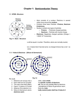
  • 1. Chapter 1: Semiconductor Theory 1.1 ATOM –Structure Usually protons and electrons will be equal in number .Therefore, atoms are normally neutral, electrically. o If an atom loses an electron, it means that it has lost some -ve charge & hence has a net + ve charge ……….. and vice versa. 1.1.1 Holes & Electrons (Silicon & Germanium) Pls recall, 1. Electrons can occupy only some fixed orbits, called shells. 2. Each shell can be occupied by only some specific number of electrons. 3. The outer most shell called valence shell, may be only partially filled by electrons. 4. Figure 1.2 gives a 2 D simplified orbital arrangement of silicon & germanium atom. 5. Absence of an electron in a shell, is defined as a hole. 6. Silicon & Germanium atoms are electrically neutral (outer shell has 4 holes & 4 electrons each) 1 Fig 1.1 Atom - Structure o Atom consists of a nucleus. Electrons in several orbits move around the nucleus.. o Contains three basic Particles –Protons, Neutrons & electrons. o Nucleus contains two types of particles o Protons : Positively charged particles. o Neutrons : Particles with neutral charge. o Electrons: Negatively charged particles (Charge = 1.602X 10⁻⁹ Coulombs). Fig 1.2
  • 2. 1.2 Electron &Hole Dynamics 1.3 N type & P type Semiconductors 1,3,1 Intrinsic semiconductor: It is very pure chemically. It has equal numbers of electrons (-ve) and holes (+ve). It has poor conductivity. 1,3,2 Extrinsic semiconductor: o When a small amount, of impurity is added to a pure semiconductor, the conductivity of the semiconductor is increased manifold. o Such materials are known as extrinsic semiconductors. o The deliberate addition of a desirable impurity, is called doping. o Doping yields two types of semiconductors viz p type and n type. o The impurity atoms are called dopants. o Such a material is also called a doped semiconductor. o Silicon & Germanium are the standard semiconductor atoms, used by the industry. Some of the popular dopants used, in doping the tetravalent Si or Ge are, Trivalent atoms such as Boron or Aluminium, for producing p type semiconductors. Pentavalent atoms such as Arsenic or Phosphorous, for producing n type semiconductors. n type: Refer fig 1.4. Pentavalent (5) impurities like Arsenic (As), Antimony (Sb), Phosphorous (P), when added to either silicon or germanium, will produce N type semiconductors. Electrons are the majority carriers. p type: Refer fig 1.5. Trivalent (3) impurities like Indium (In), Boron (B), Aluminium (Al) when added to either Silicon or Germanium, will produce P type semiconductors. Holes are the majority carriers. 2 Refer fig 1.3. o Electrons are –vely charged particles. Electrons are repelled by –ve voltage. Therefore, they will move towards a terminal where + ve voltage is applied. o Holes are +vely charged particles. Holes are repelled by + ve voltage. They will move towards a terminal where -ve Voltage is applied. o Please note the direction of the current flow is always opposite to the direction of electron flow. Fig 1.3
  • 3. Fig 1.4 n-type pentavalent atom Fig 1.5 p-type trivalent atom 1.4 pn junction Figure 1.6 shows independent p type independent n type semi-conductor. Fig 1.6 Semiconductor material n-type and p-type o Majority carriers of n type are electrons. o Majority carriers of p type are holes. 1.4.1 Diffusion Refer fig 1.7. Due to thermal agitation, electrons and holes start moving randomly, even if there is no bias. Look at the diffusion process below. Few electrons close to the junction, start crossing the junction, to reach p side Few holes close to the junction, start crossing the junction, to reach the n side These electrons combine with some holes in the p side, to create some –ve ions. These holes combine with electrons in the n side to create some +ve ions. Due to these ions, a -ve voltage build up (barrier) is created, on the p side. Due to these ions, a +ve voltage build up (barrier) is created on the n side. 3 Majority and minority carriers Majority carriers: o The more abundant charge carriers o Primarily responsible for current transport in a semiconductor. o n-type semiconductors: Electrons o p-type semiconductors: Holes. Minority Carriers: o The less abundant charge carriers o n-type semiconductors: Holes o p-type semiconductors: Electrons. Fig 1.7 shows a p type and n type conductor joined together (fabricated) to form a p-n junction o There is no external voltage (bias) applied. o Initially, pn junction is electrically neutral.
  • 4. Fig 1.7 p-n junction diode – No bias voltage This barrier voltage build up is shown in the figure 1.8. Fig 1.8 Barrier Voltage at p-n junction 1.4.2 Depletion region o In the diffusion process mentioned above, when the barrier potential is reached, further diffusion stops. o No charge carriers (electrons or holes) will be present, closer to the junction. o Only ionized atoms (+ve and –ve), will be present on either side of the junction. o This region is known as depletion region. 1.5 pn junction biasing 1.5.1 Reverse biased p-n junction Refer figure 1.9. What is reverse bias? An external dc voltage (bias) is applied to a diode such that, p side is connected to the –ve terminal and n side is connected to the +ve terminal of a battery. 4 o Barrier voltage is typically 0.7 V, for Silicon. o Barrier voltage is typically 0.3 V, for Germanium. o At around the barrier voltage, electrons (from n side) are repelled by the – ve barrier voltage in the p side. o At around the barrier voltage, holes (from p side) are repelled by the +ve barrier voltage in the n side. o Therefore further diffusion stops.
  • 5. Fig 1.9 Reverse biased p-n junction Result: Majority carriers cannot flow across junction and therefore, under reverse bias conditions, no current flow is possible. In other words, forward current does not flow. 1.5.2 Forward biased p-n junction Refer figure 1.10. What is forward bias? An external dc voltage (bias) is applied to a diode such that n side is connected to the –ve terminal and p side is connected to the +ve terminal of a battery. o This biasing arrangement decreases the barrier voltage, as shown in the figure 1.10. o Barrier voltage at n, becomes less +ve and the barrier voltage at p becomes less –ve. o Electrons (majority carriers) in the n side, are attracted across the junction, towards the p side and are attracted towards the +ve terminal. o Holes (majority carriers) in the p side, are attracted across the junction, towards the n side and are attracted towards the –ve terminal. Fig 1.10 Forward biased p-n junction 5 o This biasing arrangement increases the barrier voltage, as shown in the figure. o Barrier voltage at n, becomes more +ve and the barrier voltage at p becomes more –ve. o Electrons (majority carriers) in the n side, are repelled away from the junction and are attracted towards the +ve terminal. o Holes (majority carriers) in the p side, are repelled away from the junction, and are attracted towards the –ve terminal. o Consequently, depletion region further widens and barrier voltage increases as shown. o Consequently, depletion region decreases and the barrier voltage also reduces, as shown. Result: Majority carriers will flow across junction and therefore, under positive bias conditions, current flow is possible. In other words, forward current is flows.
  • 6. Chapter 2: Semiconductor Diodes and Applications Syllabus: Semiconductor Diodes and Applications (Text-1) : p-n junction diode, Characteristics and Parameters, Diode approximations, DC load line analysis, Half-wave rectifier, Two-diode Full- wave rectifier, Bridge rectifier, Capacitor filter circuit, Zener diode voltage regulators: Regulator circuit with no load, Loaded Regulator, Series and Shunt diode Clipping Circuits, Clamping Circuits: Negative and Positive Clamping Circuits, Numerical examples as applicable. 2.1 p-n junction diode What is a diode? Fig 2.1 Semiconductor diode with leads Draw the circuit symbol and indicate current flow. Fig 2.2 Fig 2.3 Diode size Cathode Identification Forward current (mA) Reverse voltage (V) Small- Color band or dot 100 75 Medium Diode Symbol 400 200 Large Threaded portion Few amperes Few hundreds 6 Refer fig 2.1 and 2.2 o It is a semiconductor device with a p-n Junction. o It is a one way device. o Allows current to flow when forward biased (p: + ve and n: -ve). o Almost totally blocks current flow when reverse biased (p: - ve and n: +ve). o Therefore, a diode is a 2 terminal component. o It has two electrodes called anode and cathode. o Anode is attached to p side and cathode to n side. Diodes Power classification: Refer fig 2.3. o Low power diodes: Usually small diodes can handle low currents up to 100mA. Power dissipation will be less than 800 milli-watts. o High power diodes: Large diodes can handle high currents (1 to 10 Amperes). Power dissipation will be less than 1 watt to 10 watts. o Look at the table below
  • 7. 2.2 Characteristics and parameters: 2.2.1 Diode characteristics: Refer fig 2.4 and 2.5 Fig 2.4 2.2.2 Forward characteristics (Silicon): Refer fig 2.5 Up to 0.7 V o As the forward bias is increased from 0.1 to 0.7 V, the diode hardly conducts the forward current is very low (less than 100 mA). Fig 2.5 Silicon diode – Fwd and Rev characteristics 2.2.3 Reverse characteristics (Silicon) 0 to -50 V o Please note the change of scale, in the y axis between forward & reverse characteristics. 7 o It is the study of, ‘voltage- across-the-diode’ versus ‘current- through-the-diode’. o As we know, diode is a p-n junction semi-conductor device. o When it is forward biased, diode characteristics is a study of forward voltage VF & forward current IF. o When it is reverse biased, the diode characteristics is a study of reverse voltage VR & reverse current IR. Beyond 0.7 V o As the forward bias is increased beyond 0.7 V, the forward current increases very sharply. o Increasing the forward bias beyond say 1.0 V, will destroy a diode due to excessive forward current. o A current limiting resistor is needed in the circuit to protect the diode.
  • 8. o Reverse current IR, is often very low (not more than 1 μA) for reverse voltages up to -75 V for silicon o IR is negligible compared to IF. o For all practical purposes the diode behaves like an open circuit. Beyond -75 V: o Reverse break down happens (we shall study this later). o The current increases abruptly. o This can destroy the diode, unless protected by a current limiting resistor 2.2.4 Diode characteristics (germanium) Fig 2.6 Germanium diode – Fwd and Rev characteristics 2.5 Forward & Reverse resistance : Refer fig 2.7 Fig 2.7 Problem 2.2: In fig 2.5 fig XXX calculate the reverse resistance of the silicon diode at VR =20V. At VR = 20 V, IR = 90 nA (approx) Therefore, reverse resistance (RR) = V R I R = 20V 90nA = 222 Mega ohms (approx) 2.2.6 Some of the important diode parameters. 8 Refer fig 2.6. o The characteristics are similar to that of silicon diode. o Forward voltage is 0.3 V instead of 0.7 V. o Reverse break down voltage is -50 V instead of -75 V. o Reverse current is -1.0 μA instead of -100 nA. Problem 2.1: In fig 2.6, calculate the forward resistance of the germanium diode, at IF= 60mA At IF = 60 mA, VF = 0.33 V (approx) Therefore, forward resistance (RF) = V F I F = 0.33V 60mA = 5.5 ohms.
  • 9. VF - Forward voltage drop (0.3 V for Ge and 0.7 V for silicon). IF - Forward current . VR - Reverse voltage. rd - Dynamic resistance = ΔV F ΔI F VBR - Break down voltage {50 V for Ge and 75 V for Si). PD - Power dissipation. 2.2.7 Dynamic resistance rd Recall the forward resistance that was calculated in example 2.1. RF = V F I F . This is the DC resistance of the diode, at one particular value of forward current. When the input varies by ∆VF, there will be large variation, in forward current (∆IF). This is shown in fig 2.5 Dynamic resistance rd = ΔV F ΔIF . rd is also known as ac resistance or incremental resistance There is another way of calculating dynamic resistance. It is not discussed here since it is beyond the scope of this book.The formula is rd = 26 mV IF Problem 2.3: What is the dynamic resistance of a diode with a forward current of 5 mA rd = 26 mV 5mA = 5.2 Ω. Problem 2.4: For the dynamic characteristic shown in fig 2.8, determine the dynamic resistance at 40 mA. Fig 2.8 2.3 Diode approximations: 2.3.1 Ideal Diode: In the forward bias condition It will have no forward resistance and will not drop any voltage across it. RF = 0 Ω and VF = 0 V. Refer fig 2.9 a In the reverse bias condition, an ideal diode will never have any reverse current, no matter what the reverse voltage is. VR = ∞, IR = 0 9 IF = 40 mA. Therefore, take a small interval around 40 mA as ∆IF, say from 20 mA to 60 mA. ∆VF for this range = 0.726 V - 0.71 V = 0.016 V ∆IF for this range = 60 mA - 20 mA = 40 mA rd = ΔV F ΔI F , = 0.016V 16mV = 0.4 Ω
  • 10. Therefore, what is an ideal diode? 1. Fwd Resistance = 0 Ohm 2. Fwd Voltage drop = 0 V 3. Rev resistance = Infinity 4. Rev current = 0 amp Refer fig 2.9 b and 2.9 c However, in practice, it is different as seen already in figures 2.5 and 2.6. (a) (b) (c) Fig 2.9 Diode Characteristics What are the assumptions of a near ideal diode (Si)? Fwd Voltage drop = constant Rev current = negligible (can be ignored) 2.3.2 Practical diode What is a practical diode (Si)? Fwd Resistance = 0 to 20 Ohms Fwd Voltage drop = 0.6 to 1.0 Volt Rev current = few micro amps 2.3.3 Piece-wise approximation of a diode The smooth diode curve of fig 2.5 or 2.6 can be approximated by taking samples at very close intervals and interconnecting adjacent samples through short straight lines. Problem 2.5: Construct a piece wise linear characteristics of a germanium diode, given that its dynamic resistance is 0.6 Ω and forward current is 100 mA . Look at fig 2.10 10
  • 11. Fig 2.10 Join A B. The piece wise linear characteristic is the thick line segment shown. 2.3.4 DC equivalent circuits of a diode Fig 2.11 Some equivalent circuits of diodes are shown in fig 2.11 and 2.12. Eqvt circuit of an ideal diode is shown in Fig 2.12 (a) . In fig 2.12 (b) a practical diode with specific voltage drop VF =0.7 V (Si) or 0.3 V (Ge) is shown. Has a constant VF and negligible DC resistance (Zero) (a) (c) (b) Fig 2.12 Diode Equivalent circuits In fig 2.11(c), a more complete equivalent circuit, with a specific VF and a specific rd is shown. rd represents the VF part. Fig 2.13 Ideal diode. VF = 0.7 V (Silicon, by default), IF = 10 mA (given) 11 It is a Ge diode. VF = 0.3 V Mark Point A = (0.3 V, 0 mA) How to find B? ∆IF = 100 mA – 0 mA = 100 mA ∆VF = ∆IF X rd = 100 mA X 0.6 Ω = 60 mV. = 0.06 V Point B = {(0.3 V + 0.06 V), 100 mA)} = {(0.36 V, 100 mA)} What is an equivalent circuit? The electrical behaviour of the given circuit is accurately modelled using a combination of, simple electrical components such as Resistor (R), Inductor (L) and Capacitor (C). Why equivalent circuit? Equivalent circuit simplifies analysis of a complex circuit. Problem 2.6: For the fig 2.13, what will be the drop across the silicon diode, if IF = I0 mA and dynamic resistance is 0.8 Ω.
  • 12. Drop across rd = IF X r d = 10 mA X0.8 Ω = 8 mV. Total drop across the diode = 0.7 V + 8 mV. = 0.708 V. Problem 2.7: In the circuit shown in fig 2.14, calculate IF . (Unless otherwise mentioned, the diode is silicon by default. E = IF.R + VF 10 V = (IF X 2.2K) + 0.7 V  IF = 10V −0.7V 2.2K = 4.22 mA. Problem 2.8: For the same circuit in fig 2.14, what is the new IF if the diode has a dynamic resistance of 0.3 Ω and R = 5 Ω . The circuit is redrawn in fig 2.15. E = IF.R + IF.rd + VF 10 V = (IF X 5 Ω) + (IF X 0.3 Ω) + 0.7 V I F = E−V F R+rd = 10V –0.7V 5 Ω+0.3Ω = 9.3 V / 5.3 Ω = 1.76 A Fig 2.14 Fig 2.15 2.4 D C load line analysis (Diodes) This topic mainly revolves around three subtopics a) DC Load line b) Diode V-I Characteristics c) Q point. 2.4.1 How to draw a DC Load line? Refer fig 2.16 As per Kirchoff’s Law, E ▬ (IF X RL) ▬ VF = 0 E ▬ VF = IF X RL E RL ▬ V F RL = IF 12
  • 13. IF = VF (−1 RL ) + E RL Fig 2.16 E RL for a given circuit, is a constant.(say C) IF = VF (−1 RL ) + C This is of the form y = mx + c (Straight line equation).where slope m = ▬ 1 RL The variables are the DC conditions, IF and VF. Hence the name, DC load line. Problem 2.9: Let us draw a DC load line for the ckt in fig 2.16 where E = 6 V and RL = 150 Ω E = (IF X RL) + VF 6 V = 150 IF + VF ( A) If IF = 0, Then VF = 6 V. For a diode, VF = 6 V is of course absurd but a DC load line does not take the device characteristics into account  Point A = (6 V, 0 mA) ( B) If VF = 0, Then IF = 6V 150 Ω = 40 mA. Point B =(0 V, 40 mA) Draw a graph using the above values. o A has coordinates VF = 6 V , IF = 0 mA. o B has coordinates VF = 0 V , IF = 40 mA. o Join AB as a Straight line. o This is the load line. o Note, slope of this load line = m = ▬ 1 RL 2.4.2 Diode VI characteristics This is the same curve in fig 2.5 and 2.6 Diode VI characteristic is the forward bias region (first quadrant). This curve is super- imposed on the D C load line drawn above. 2.4.3 Q point (Quiescent point, DC bias point) This is the point of intersection of DC load line and the diode V-I characteristics. 13 Fig 2.17 Problem 2.10: The Q point is (0.7 V , 35.3 mA). How? For a silicon diode, VF = 0.7 V. Recall from fig 2.16, 6 V = 150 IF + VF 6 V = 150 IF + 0.7 V 5.3 V = 150 IF IF = 35.3 mA  Q point is (0.7 V , 35.3 mA).
  • 14. Problem 2.11: Find the load resistance for this circuit in fig 2.19, for IF = 20 mA 1) Draw Load line VF = E- IF RL a) For IF = 0, VF = E = 7.7 V.  Plot A at (7.7 V , 0 mA) b) Next, plot Q (Inter-section of diode characteristics and IF = 20 mA line) c) Join AQ and extend it to B. You will find B intersecting Y axis at IF = 22 mA Why? Let us find IF through circuit analysis Problem 2.12: What is R L from the load line? We know that VF= E - IF RL ∆V F = 7.7 V - 0.7 V = 7.0 V. ∆I F = 20 mA – 0 mA = 20 mA. RL = ΔV F ΔI F = 7V 20mA = 350 ohms Using the equation VF = E – IF RL When V F = 0, E = IF R L 7.7 V = IF X 350 Ω I F = 7.7 V / 350 Ω = 22 mA. 14 Fig 2.18 For the given circuit this Q point is fixed Conclusion: (1) For a given VF and IF, the Q point is unique. (2) VF for diodes is generally constant (0.7 V for Si and 0.3V for Ge) (3) Therefore, for altering the Q point IF should be changed (4) IF can be changed by either changing Input voltage E or RL Fig 2.19 Fig 2.20
  • 15. 2.4.4 Diode Parameters 1. IF (max) - Maximum forward DC current permissible 2. VF - Forward voltage drop (0.7 V for Si and 0.3 V for Ge) 3. VBR - Maximum reverse voltage that can be applied, beyond which break down occurs 4. rd - Dynamic resistance 5. IR - Reverse saturation current (current flow when diode is reverse biased ) 6. Knee voltage - that forward voltage beyond which, forward current increases exponentially 7. P - continuous maximum power dissipation permissible at 25 deg C 2.5 Rectifiers Define ‘’Rectifier’’ Rectifier is a device such as diode, that converts alternating current to direct current (ac to dc). How is diode rectification done? The rectification is done, by converting ac current to dc current, by suppression or inversion of alternate half cycles. 2.5.1 Half wave rectifier (HWR): Look at figure 2.21. A simple half wave rectifier is shown. 15
  • 16. HWR Operation Refer fig 2.21 o The input is fed through a transformer primary (terminals 1 and 2.). o During +ve cycle of input, terminal 3 is +ve and terminal 4 is –ve. o Diode gets forward biased and the current flow is clock wise, as shown in fig (a). o Output voltage is IL RL. o During – ve cycle of input # 4 is +ve and # 3 is –ve. Diode is reverse biased and diode behaves like an open circuit, as shown. No current flows in the circuit. o The output voltage is zero. The peak inverse voltage across diode is, the input voltage (peak value). o The Wave forms are shown in fig 2.21 Problem 2.13: For the circuit shown, determine the peak output voltage, peak load current and diode peak inverse voltage. The ac input is 10V, the load resistance is 1 kΩ and the diode is germanium. 16 Fig 2.21 Half-wave rectifier
  • 17. Input voltage is 10 V rms. Input peak voltage: Vp in = 2 X 10 V = 14.14 V Output peak voltage: Vp out = Vp in - VF = 14.14 - 0.3 V [Germanium] = 13.84V Peak inverse voltage = PIV = Vp in =14.14 V. 2.5.2 Full wave rectifier (FWR): o As the name implies rectification happens, for both +ve and –ve cycles of the input wave. Full wave rectifier, therefore, uses 2 diodes. o A transformer input full wave rectifier (FWR) is shown in fig 2.23. The transformer becomes complex, with a centre-tap operation. FWR Center tap transformer: Look at fig 2.23. Fig 2.23 Center-tap transformer FWR Operation: A full wave rectifier using two diodes is shown in fig 2.24. NOTE center tap is at ground (0V) potential. Note, diode anodes are returned to ground through the load resistor RL Input: + ve half cycle (Refer fig 2.25) o Terminal 3 is +ve, with respect to ground (center tap) and D1 is forward biased. 17 Important : Unless otherwise mentioned, the input is always specified as rms. The relation between peak value & rms value is Vrms = Vpeak / √2 and Irms = Ipeak / √2 and so on. Fig 2.22 It consists of a primary winding (1,2) and two secondary windings (3,4 and 5,6) One end of, each of these secondary windings, is joined together. In the figure 4 and 5 are joined. The windings normally have the same number of turns and therefore the 4, 5 junction becomes truly a center tap. The sense of these two secondary windings is in such a way, that the two secondary outputs always oppose each other, in phase.
  • 18. o Terminal 6 is –ve, with respect to ground (center tap) and D2 is reverse biased. o Current flows in the Dl loop as shown. (IL1) o Resultant output (Vout1) is a +ve half cycle (Same phase as input). Input: - ve half cycle (Refer fig 2.26) o Terminal 6 is +ve, with respect to ground (center tap) and D2 is forward biased. o Terminal 3 is –ve, with respect to ground (center tap) and D1 is reverse biased. o Current flows in the D2 loop as shown. (IL2) o Resultant output (Vout1) is a +ve half cycle (Inverted phase as input). o The load current flows through RL in the same direction (right to left) whether the input is a +ve half cycle or –ve half cycle. The wave forms are shown in the figure. The load current is, the sum of the individual diode currents. o Waveforms are shown in fig 2.27. Fig 2.24 Full-wave rectifier Circuit (Two diodes) 18 2.5.2.3 Transformer related parameters Let input voltage be Vp = Vpm sin wt. Let wt =α  Vp = Vpm sin α (primary) Vs= Vsm sin α. If the transformer has a turns ratio Np : Ns, then NS NP = V SM VPM
  • 19. Fig 2.27 Full-wave rectifier waveforms Transformer secondary resistance: The winding resistance Rs of transformer secondary, often comes into play during current power calculations. . Problem 2.14: If the transformer in the previous example is used, what is the peak secondary current in this circuit in fig 2.28? Assume secondary has a resistance of 5 ohms. Fig 2.28 Fig 2.29 Secondary peak voltage = 32.52 V. (previous example) . Refer equivalent circuit in fig 2.29. Look at secondary equivalent circuit im = V S RS+Rf +RL ipeak (secondary) = 32.52V 5 Ω+10 Ω+1000Ω = 32 .52 V / 1015 ohms = 32.04mA - 19
  • 20. 2.5.3 RECTIFIERS EQUATIONS (Refer fig 2.30) DC Current Idc Idc= 1 2π ∫ 0 π Im sin α dα ¿ Im 2 π [−cosα ]0 π ¿ −Im 2π [−1−1] Idc= Im π Idc= Vm π(Rf +RL+RS) DC Current Idc Idc= 1 π ∫ 0 π Imsin α dα ¿ Im π [−cosα ]0 π ¿ −Im π [−1−1] Idc= 2Im π Idc= 2Vm π(Rf +RL+RS) DC output Voltage Vdc Vdc=Idc RL= IM π RL ¿ V M π (1+ Rf RL ) ( Assume RS=0) DC output Voltage Vdc Vdc=Idc RL= 2I M π RL ¿ 2V M π (1+ Rf RL ) ( Assume RS=0) RMS current I RMS current I 20 Fig 2.30 Fig 2.30
  • 21. I= √ 1 2π ∫ 0 2π i 2 dα I= √ 1 2π ∫ 0 π Im 2 sin 2 α dα I= Im 2 I= √1 π ∫ 0 π i 2 dα I= √1 π ∫ 0 π Im 2 sin 2 α dα I= IM √2 RMS output voltage across load Vrms=I ×RL= Im 2 ×RL Vout= V M 2 (1+ Rf RL ) RMS output voltage across load Vrms=I ×RL= IM √2 ×RL Vout= V M √2 (1+ Rf RL ) DC Output Power Pdc=Idc 2 RL= Im 2 RL π 2 ¿ Vm 2 RL π 2 (RL+Rf ) 2 DC Output Power Pdc=Idc 2 RL= 4 Im 2 RL π 2 ¿ 4Vm 2 RL π 2 (RL+Rf ) 2 Total AC Input Power PDiode=I 2 Rf = Im 2 4 Rf PRL=I 2 RL= Im 2 4 RL P¿=PDiode +PRL ¿ Im 2 4 (Rf +RL) Total AC Input Power PDiode=I 2 Rf = Im 2 2 Rf PRL=I 2 RL= Im 2 2 RL P¿=PDiode +PRL ¿ Im 2 2 (Rf +RL) Rectifier efficiency N= Pdc P¿ = (Im 2 π 2 × RL) ⌈ Im 2 4 (Rf +RL )⌉ ¿ 4 π 2 RL Rf +RL ¿ 0.406 1+ (Rf RL ) ¿ 40.6 1+ (Rf RL ) Rectifier efficiency N= Pdc P¿ = (4 Im 2 RL π 2 ) ⌈ Im 2 2 (Rf +RL )⌉ ¿ 8 π 2 RL Rf +RL ¿ 0.812 1+ (Rf RL ) ¿ 81.2 1+ (Rf RL ) Ripple Factor r= Iac Idc Ripple Factor r= Iac Idc 21
  • 22. Please Note I 2 =Idc 2 +Iac 2  r= √I 2 −Iac 2 Idc = √( I Idc ) 2 −1 ¿ √(Irms Idc ) 2 −1 Form Factor This is defined as F= I Idc F= (I M 2 ) (I M π ) = π 2 =1.57 Hence Ripple Factor r=√F 2 −1 r=√1.57 2 −1 r=1.21 Form Factor This is defined as F= I Idc F= I Idc = (IM √2) (2 IM π ) =1.11 Hence Ripple Factor r=√F 2 −1 r=√1.11 2 −1 r=0.48 Transformer utilization factor (TUF) What is transformer utilization factor? DC Power delivered TUF= ¿load AC Power ratingof transformer ¿ Half wave Rectifier Full wave Rectifier PDC =IDC 2 ×RL=(Im π ) 2 ×RL PDC =IDC 2 ×RL=(2 Im π ) 2 ×RL Pac(rms)=Vrms ×Irms Pac(rms)=Vrms ×Irms Pac (rms)= V M √2 × IM 2 Pac (rms)= V M √2 × I M √2 Im= V M RS+Rf +RL But Vm = ImRL But Vm = Im x RL  TUF = (Im 2 RL π 2 ) (Im 2 RL 2√2 )  TUF = (4 π 2 ×Im 2 RL ) (Im 2 RL 2 ) = 2√2 π 2 = 0.287 = 8 π 2 = 0.812 Problem 2.15 : The input signal is 50v in amplitude 22
  • 23. with a frequency of 50 HZ. Calculate (a) Rectifier efficiency (b) Ripple Factor Refer fig 2.31, Before we find m, we need to find (a) Peak, Average (DC) and rms values of load current (b) DC power output (c) AC Power input (d) Note, there is no transformer,  Rs = 0 (a) Peak load current = Im= Vm Rf +RL+RS = 50 20+980 = 50mA Idc= Im π = 50 3.14 =15.92mA=15.92×10 −3 A Irms= Im 2 = 50 2 =25mA=25×10 −3 A (b) VDC =IDC × RL=15.92×10 −3 ×980=15.6V PDC =IDC 2 ×RL=15.92 2 ×980=248.4mW (c) AC Power input = (Irms) 2 ×(RL+Rf ) = (25×10 −3 ) 2 ×(980+20) = 625 mw (d) Rectifier efficiency = Pac∈¿ Pdc ¿ = 248.4 mW 625mW = 39.74% (e) Ripple factor = √(Irms Idc ) 2 −1 = √( 25mA 15.92mA ) 2 −1 = 1.21 (f) % regulation = V noload−V fullload V load X100 (g) Vno load = VDC = V m π = 50 π = 15.91 V (h) Vload = VDC = 15.6 V (j) Therefore % regulation = 15.91−15.6 15.6 = 1.98% Problem 2.16: For the example 2.14, already solved, find (a) Peak, average & rms load currents (b) DC Power output & ac power input (c) Efficiency (d) Form factor (e) Ripple Factor Refer fig 2.32. From 2.14, the peak secondary voltage Vm = 32.52 V 23 Fig 2.31 Fig 2.32
  • 24. (a) Peak, average & rms load Im= Vm RS+Rf +RL = 32.52 5+10+1000 = 32.52 1015 = = 32.04mA IDC= Im π = 32.04mA π =10.2mA Irms= Im 2 = 32.04 mA 2 =16.02mA (b) DC Power output & ac power input VDC =IDC × RL=10.2mA ×1000=10.2V PDC =(IDC ) 2 × RL=(10.2mA)2 ×1000=104 mW ac∈¿=(Irms ) 2 ×(RS+Rf +RL)=(16.02)2 ×(5+10+1000)=260.5mW P¿ (c) Efficiency Pac∈¿ = 104 mW 260.5mW ¿ PDC ¿ = 39.92% (d) Form factor ¿ Irms Idc = 16.02mA 10.02mA = 1.57 (e) Ripple Factor ɤ ¿√F 2 −1=√1.57 2 −1=1.21 Problem 2.17: The input to a full wave rectifier is 25 sin 100t. The load resistor is 200. Silicon diodes (0.6 V) with 50 Ω diode resistance is used. What is the peak output voltage, peak current and peak inverse voltage? The diodes are silicon (0.6 V). What is the frequency of the signal? Input = 25 sin 100t, Compare this with V = Vm Sin t. Vm = 25V (peak)  = 2ft = 100t f = 50Hz Input voltage (peak) = 25 V Output voltage (peak) = 25 V ─ VF = 25 V ─ 0.6 V = 24.4 V Output Current = 24.4V/(200 + 50) = 97.6 mA PIV = Peak inverse voltage is the voltage across the diode, during reverse bias conditions PIV of FWR = 2VM= 2 X 25 V= 50 V Problem 2,18: In a full wave rectifier the secondary of the transformer used is 10 – 0 – 10 V. The secondary resistance is 20. The diodes have forward resistor of 20  and load resistor of 170  (a) Calculate Peak, average and rms currents, (b) Calculate DC output power, ac input power and efficiency (c) Calculate form factor, ripple factor and % regulation. The secondary of a FWR is from a center tapped transformer. Look at the figure 2.33 30V is the rms value (not peak value) The diode is fed through one half of the secondary (0 – 30 V)  RMS input for each diode Vrms=30V 24
  • 25. Vm=30×√2=42.42V Im= Vm RS+Rf +RL Secondary resistance given = 20  (for full secondary) Rs.= 10  for each half of the secondary. IM= 42.42V 10+20+170 = 42.42V 200 =212mA IDC= 2I M π = 2×212mA π =134.9mA Irms= I M √2 = 212mA √2 =149.9mA PDC =IDC 2 ×RL=(134.9)2 ×170=3.1W ac∈¿=Irms 2 ×(RS+Rf + RL )=(149.9)2 ×(10+20+70)=4.49W P¿ ¿ PDC Pac = 3.1W 4.49W ×100=69 Form Factor ¿ Irms I DC = 149.9 134.9 =1.11 Ripple Factor ¿√(F) 2 −1=√(1.11) 2 −1=0.48 % Regulation ¿ V NL−V FL V FL VDC (NoLoad)= 2VM π = 2×42.42 π = 27 V VFL=IDC ×RL=134.9×170=22.9V % Regulation ¿ 27V −22.9V 27V ×100=15.2 2.5.4 Bride rectifier (BR) What is a bridge in a bridge rectifier? A Basic bridge rectifier is shown in fig 2.34 It is an arrangement of 4 diodes in such a way that o full wave rectification happens o 2 diodes conduct during the +ve input cycle and Fig 2.34. Bridge. the other two diodes conduct during the -ve input cycle. It is a full wave rectifier . It consists of 4diodes o It does not require a center tap secondary. o Input is applied in the primary (#1, #2 ) BR Operation: A bridge rectifier is shown in fig 2.35 25 Fig 2.33 Equivalent Circuit
  • 26. Fig 2.35 Bridge Rectifier Circuit Fig 2.35(a) Bridge Rectifier Circuit (Redrawn) The same bridge rectifier is redrawn to provide more clarity in fig 2.35(a). Fig 2.36 Bridge Rectifier( +ve cycle) Fig 2.36(a) Bridge Rectifier( -ve cycle) +ve cycle: When the input is a +ve cycle, top of the secondary is +ve and the bottom is –ve. Diodes D1 and D3 will conduct as shown in fig 2.36. ─ ve Cycle: When the input is a -ve cycle, bottom of secondary is +ve and the top is –ve. Diodes D2 and D4 will conduct as shown in fig 2.36(a). Note, the current through RL, is in the same direction (right to left), in both cycles Equations of bridge rectifier: 26
  • 27. They are same as that of FWR, except Im Im = Vm Rs+Rf +Rf +RL [ since, 2 diodes are involved, per cycle] IDC = 2 Im ❑ , VDC = 2 V m ❑ , Irms = Im √2 PDC = (IDC)2 X RL = 4 ❑ 2 Im 2 RL Pac = I2 RMS (RS + 2 Rf + RL) = Im 2 2 [RS + 2Rf + RL] Efficiency (η) = 8 ❑ 2 [ RL / (RS + 2Rf + RL) ] % = 81.2 % F = 1.11, = 0.48,ϒ TUF = 0.812 2.6 Comparison of rectifiers Compare advantages & disadvantages of all the three rectifiers. H W F W Bridge Only one diode. Easy design. 2 diodes. Complex design. 4 diodes. Complex design. No centre-tap transformer Centre-tap transformer No centre-tap transformer Ripple factor high. (1.21) Ripple factor Low. ( 0.48) Ripple factor low. (0.48) TUF low. Inefficient. TUF High. Efficient. TUF high. Efficient. Low efficiency 40.6%. High efficiency 81.2%. High efficiency 81.2%. Output load voltage & current low Output load voltage & current high. Output load voltage & current high. Uni-directional current through transformer. Therefore transformer can saturate. No net dc current through transformer. Therefore transformer will not saturate. Current is continuous always hence transformer can be small & Inexpensive. PIV of diode low (Vm) PIV of diode high (2 Vm) PIV of diode low (vm) Example 2.19: In a bridge rectifier, the transformer primary voltage is 200 sin wt. The transformer step down ratio is 4 : 1. The secondary resistance is 10 ohms. Forward resistance of the diode is 20 ohms and the load resistance is 450 ohms. Calculate Im, IDC, Irms, VDC, Ripple factor, Efficiency (η) and PIV of the diode. Vp = 200 sin wtN1: N2 = 4 : 1  Vs = 200sin wt 4 = 50 sin wt Vm =50 V. Im = V m Rs+2Rf +R L = 50V 10+(2X 20)+450 = 100 mA IDC = 2 Im π = 200 π = 63.6 mA 27
  • 28. Irms = Im √2 = 100 1.414 = 70.7 mA VDC = IDC X RL = 63.6 X 450 = 28.6 V PDC = (IDC)2 X RL = (63.6)2 X 450 = 1.82 W Pac = Irms 2 X (Rs + 2 Rf + RL) = (70.7)2 X (10 + 40 + 450) = 2.49 W Efficiency = PDC Pac % = 1.82W 2.49W % =73.09 % Ripple factor = √(Irms Idc ) 2 −1 = √(70.7 63.6) 2 −1 = 0.4854 PIV for a bridge rectifier = Vm = 50 V 2.7 Rectifiers: Quick reference guide Parameters HW FW BR Load current Im Vm Rs+Rf +R L Vm Rs+Rf +R L V m Rs+2Rf +R L IDC – Average DC current Im π 2 Im π 2 Im π VDC - Average DC voltage V m π 2Vm π 2Vm π Irms Im 2 Im √2 Im √2 Vrms V m 2 V m √2 V m √2 PDC - DC Power output (Im π ) 2 (2Im π ) 2 (2Im π ) 2 Pac - AC Power output (Im 2 ) 2 (Rs+Rf +RL) (Im √2 ) 2 (Rs+Rf + RL) (Im √2 ) 2 (Rs+2Rf +RL) Efficiency 40.6% 81.2% 81.2% Form factor 1.57 1.11 1.11 Ripple factor 1.21 0.482 0.482 TUF 0.287 0.812 0.693 Ripple freq f 2f 2f PIV Vm 2 Vm Vm 2.8 Capacitor Filter Circuit 2.8.1 Half-wave rectifier with Capacitor filter 28
  • 29. Fig 2.39 shows a HW rectifier, with a capacitor filter. Let us assume an ideal diode . VF =0 Operation Why ? (Refer fig 2.40 and 2.41) o Let us say the sine wave has a peak voltage Vm =5 V. Up to P, the capacitor charges, simply following the input voltage. Therefore, the capacitor voltage will be 5V at P. o The input voltage starts reducing beyond P (< 5 V). But the capacitor is already at 5V. Therefore, the diode finds itself getting reverse biased beyond P. o Refer fig 2.40. The capacitor slowly discharges from its 5 V, through the resistor RL The rate of discharge is determined by the time constant RLC. Greater the time constant, slower will be the discharge. What happens in Cycle 2? (Refer Diagram 2.39.) o The capacitor is fully charged up to 5 V at P. The capacitor discharges in the rest of the cycle 1 and up to Q in cycle 2. o Let us say, at Q the capacitor has discharged up to 4 V. o The input also is at 4V at Q and rising. Look at interval QR. In this interval, the input will be more +ve than the capacitor. The diode gets forward biased in QR. Consequently the capacitor charges again by following the input. At R, the input is 5 V & the capacitor also is at 5 V. o Beyond R, the input voltage will be less than that of capacitor. Diode is reverse biased. Capacitor starts its slow discharge. This cycle keeps repeating. 29 What happens in cycle 1? 0 to 90 deg (Refer fig 2.38) o Input is switched on. During the first quarter positive cycle (0 to 90 deg) of the input, the diode conducts and the capacitor charges to the peak value of the input . 90 deg to 360 deg [Refer fig 2.38(a)] o From 90 deg to 360 deg of the first cycle the diode does not conduct . Fig 2.37
  • 30. Fig 2.39 HWR Capacitor filter action (2 cycles) 2.8.2 Full wave rectifier with capacitor filter Time constant o The capacitor in HW rectifier, has two time constants, one for charging and one for discharging. o Charging is through the diode whose resistance Rf is very low. o Time constant is small and the capacitor charges very quickly. (Imagine filling up a bucket with a very large inlet tap). o Discharging is through the resistor RL whose value is very high. o Time constant is large and the capacitor discharges very slowly. (Imagine emptying the bucket through a very small outlet tap). The theory is exactly similar to HW rectifier discussed earlier. The circuit diagram and the wave forms are shown. FWR with filter diagram is shown in fig 2.40. Wave forms are shown in fig 2.40(a) Fig 2.40(a) FWR - Capacitor filter action (2 cycles). Why capacitor filter? 30 Fig 2.40 Fig 2.40
  • 31. Output ripple will be less as seen above. The rip nle factor , frequency, capacitor value and theϒ load resistor are inter-related by the equation, =ϒ 1 4√3Cf RL Example 2.20: If a full wave rectifier is fed a sine wave of 10 V, 400 Hz, what is the capacitor value required, if the load current required is 20 mA and ripple factor is 2 % Full wave rectifier .Ripple = 2f = 800 Hz. What is RL? VDC = 2Vm π IDC X RL = 2Vm π RL = 2Vm π X 1 I DC Sine wave i/p = 10 V (rms) [unless otherwise mentioned V is rms] Vm = 10 V X √2 = 14.14 V IDC = 20 mA RL = 2 X 14.14 20 X20 X 10 −3 = 450 Ω Ripple factor ϒ = 1 4√3Cf RL 2 100 = 1 4 X 1.732 X 800 X 450 = 2 X 10-5 = 20 micro farad (μF) 2.7 Zener diode voltage regulator 2,7,1 Zener characteristics 31 Refer fig 2.41 o Zener diode is a special type of diode. o It is widely used as a voltage reference in DC regulated power supplies o Zener is always used in the reverse bias conditions. o When the reverse bias exceeds a specified value, reverse current (IR) flows, almost unlimited. o This voltage is called break down voltage or Zener voltage or Knee voltage. o The Zener diode circuit Symbol is shown here. Fig 2.41 Zener Diode - Symbol , biasing and current flow
  • 32. 2.7.1.1 Fwd characteristics: The forward characteristics is same as that of a normal diode. 2.7.1.2 Rev characteristics (refer fig 2.42 and 2.43) o The diode is operated in reverse bias mode (Anode: – ve, Cathode: +ve). o Up to some reverse voltage, reverse current is low. o Beyond a specific reverse voltage, the pn junction breaks down. o This is known as Zener break down. o Large unlimited reverse current flows. o The zener diode maintains a steady voltage over a large current range as seen in the figure. o It is necessary to limit the current by using a series resister R1. o The break down action is reversible. Zener diode can be used again and again. Fig 2.42 Zener Diode Characteristics Fig 2.43 What is the zener current in this circuit without a load resistor? (fig 2.43)? Iz = E−VZ R1 What is the zener current in the circuit in fig 2.44, with a load resistor RL? What is the load current in this circuit? Iz + IL = E−Vo R1 = E−VZ R1 IL = V Z RL 2.7.2 Zener break down mechanism Case 1 Very narrow depletion region o Reverse voltage produces very high field strength. o What is field strength? Voltage per distance (Volts / Distance.) o Electrons break away from their atoms due to this field strength. o Due to this electron flow, depletion region is converted into a conductor (from insulator) o This is called ionization by electric field 32 Fig 2.42
  • 33. o This is one of the Zener break down mechanisms o Usually occurs when reverse bias is < 5V Fig 2.44 2.7.3 Power dissipation of a Zener What is maximum power dissipation PD of a Zener? The Zener operates in a break down mode. (Reverse bias). Once break down happens, current through the Zener is unlimited. This current should be limited through a resistor. Otherwise Zener will dissipate too much power, get heated and burn itself out. Power dissipated in the Zener PD = VZ X IZ (refer figure 2.44) Every Zener has a specification for Maximum power dissipation PD max and the designer should ensure that the Zener is (by operated with in PD max (by choosing E & R carefully) Example 2.17: What should be value of R, in fig 2.45, if the Zener break down voltage is 8 V and PD max = 400 mW Fig 2.45 Example 2.18: VZ =10V, R =500. For this circuit in fig 2.46, what is the current through the Zener? What is PD of Zener? 33 Case 2 Depletion region very wide o In the reverse bias mode reverse saturation current flows. o There are electrons moving in reverse saturation current. o When these electrons travel in the wide depletion region, these electrons gain a lot of energy o These energetic electrons collide with atoms and cause their electrons to break-free. o Due to these new electrons, more collisions occur and more electrons get released o This is known as Avalanche break-down. o Also known as Ionization by collision o Usually occurs when reverse voltage is > 5V PD = VZ X IZ 400 mW = 8 V X IZ  IZ = 50 mA The resistor must ensure IZ is < 50 mA Input voltage = 12 V Zener voltage = 8 V Voltage across resistor R = 4 V Current through resistor R = 50 mA Value of R = 4V 50mA = 80  R = 80 
  • 34. Fig 2.46 2.7.4 Equivalent circuit of Zener DC Equivalent circuit Fig 2.47 Fig 2.48 Example 2.19: A Zener has a break down voltage of 5 V and a dynamic Impedance (Zz) =30 ohms. Zener current is 25 mA. How much will the Zener voltage change when the Zener current changes by ±10 mA? (Refer fig 2.48) Vz = 5 V, Iz = 25 mA, ∆IZ = ±10 mA, Zz =30 ohms. ∆VZ = ∆IZ X Zz = ± 10 mA X 30 ohms = ±300 mV VZ ( Maximum) = VZ + ∆VZ = 5 V + 300 mV = 5.3 V VZ (Minimum) = VZ - ∆VZ = 5 V - 300 mV = 4.7 V 2.7.5 Zener diode voltage regulator What is a voltage regulator? A voltage regulator ensures that the output voltage is constant for the following conditions. a) When the input voltage is varied between a specified minimum & maximum range. b) When the load current is varied from no load (0 A) to its rated full load current. In practice, the output voltage cannot be rock steady. It will have minor variations up and down. Example 2.20: How a 5V, 200 mA regulator behaves typically, when input voltage varies Voltage regulation (example) Input voltage 12 V 10 V 8 V Output Voltage 5.1 V 5.0 V 4.9V 34 VZ = 10 V. R = 500   Voltage across resistor = 15 V – 10 V = 5 V Current through R = 5V 500 = 10 mA Current thro Zener also = 10 mA PD of zener = VZ X IZ = 10 V X 10 mA = 100 mW. ac Equivalent circuit Recall, diode has a dynamic resistance (rd). Similarly, zener also has a dynamic impedance (Zz)
  • 35. Example: How a 5V, 200 mA regulator behaves typically, when load current varies Current regulation Load Current 200 mA 100 mA 0 mA (no load) Output voltage 5.0 V 5.1 V 5.2 V How zener diode acts as a regulator? Refer Fig 2.49 (only reverse characteristics) Fig 2.49 o The zener requires a certain minimum current, to break-down and act as a regulator. In this example, the minimum current required, is shown as 5 mA. o Similarly, the zener cannot support, beyond a certain maximum current. Else, it will exceed its maximum permissible power dissipation. In this example, maximum current is 40 mA. o Usually, it is prudent to operate the zener, halfway between these two extremes. 2.7.6 Zener diode as a shunt regulator. Example 2.21: Find out I, Iz and IL for this circuit in fig 2.50 We are sure of two nodes here. Node A = 12 V Node B = VZ = 6 V Fig 2.50 35 Recall, zener diode operates in the reverse bias conditions. o When reverse bias reaches VZ (5 V in this example), zener break down happens and the reverse current shoots up. o The zener voltage is steady around 5.0 V, even though the current varies from 2 mA to 40 mA and beyond. o This shows that zener can, always maintain a constant voltage across it, for a wide range of current variations through it. o This is the property of a good voltage regulator a) Find IL Voltage across R L = Voltage of Zener VO = VZ = 6 V IL = V Z RL = 6 V / 2K = 3 mA b) Find I (current through Rin) One end of Rin is Node A and the other end is Node B. Rin =1 K Voltage across Rin =VA –VB = 12 V – 6 V = 6 V. Current through Rin = 6 V / 1K = 6 mA c) Current thro Zener I = IZ + IL 6 mA = Iz + 3 m A  I Z = 3 m A.
  • 36. Fig 2. 51 Example 2.22: Calculate the input voltage range for which output will be constant, for the circuit in fig 2.51. The zener must operate between 5mA and 20mA. RL = 2.5 K, Vz = 5  IL = 5 V / 2.5 K = 2 mA. Note IL is always 2 mA in this circuit. 1) Calculate Vin min 2) Calculate Vin max Vin min happens when IZ is min = 5 mA I = IL + IZ min = 2 mA + 5 mA = 7 mA The current thro R in = I = 7 mA Voltage drop across Rin = I X Rin = 7 mA X 1K = 7 V  Vin (min) required = Voltage across Rin + VZ = 7 V + 5 V = 12 V Vin max happens when IZ is max = 20 mA. I = IL + IZ max = 2 mA+20 mA = 22 mA The current thro R in = I = 22 mA Voltage drop across Rin = I X Rin = 22 mA X1 K = 22 V …Vin ( max ) = Voltage across Rin +VZ = 22 V + 5 V = 27 V. Example 2.23: The zener in fig 2.51(a), is required to deliver a load current of 30 mA at a constant output voltage of 6 V. The minimum current of the zener is 5 mA. PD max of zener is 240 mW. The input varies between 10 V to 12 V. What should be the value of the series limiting resistor? Fig 2.51(a) 36 RL = 30 mA, Voul = 6 V = Vz, PD max = 240 mW, IZ min = 5 mA, Input : 8 V to 10 V, I L =20 mA 1) To find Iz max Iz min = 5 mA (given) but what is Iz max? PD max = 240 mW (given). PD = Iz max X VZ 240 mW = Iz max X 6 V Iz max = 40 mA 2) To find Imax and Imin Imax = Iz max + IL = 40 +20 = 60 mA Imax = Iz min + IL = 5 + 20 = 25 mA 4) To find R max ? Rmax happens when Vin is minimum and I is Imin Vin(min ) = Vz + Imin Rmax 10 V = 6 V + 25 mA X Rmax R max = 4V 25mA = 160  The value of R should be between 100  and 160 .
  • 37. Relationships to remember. 1. How to find Iz max? Use the relation: PD = Iz max X VZ 2. How to find Imax and Imin? Use the relation Imax = Iz max+IL & Imax = Iz min+ IL. 3. How to find Rmin? Rmin happens when when Vin is max and I is Imax 4. How to find Rmin? R max happens when Vin is min and I is Imin 5. How to find Vin max and Vin min? Use the relation Vmax = Vz + Imax Rmin & Vin(min) =Vz + Imin Rmax 2.8 Series and shunt diode clipping circuits What is clipper? o A circuit, which removes unwanted segments of a wave-form, is called a clipper. o A clipper is also known as a limiter. o A half wave rectifier is an example of clipper which clips one half cycle of the input. o Diodes are used in clippers. o If the diode is in series with the load, it is called a series clipper. o If the diode is in parallel with the load, it is called a parallel clipper. 2.8.1 Series clippers (refer fig 2.52) The diode is series with the load. If the + ve part of the input signal is clipped off, it is a +ve clipper. If the – ve part of the input signal is clipped off , it is a –ve clipper. 2.8.1.1 Series –ve clipper (Silicon Diode) 37 3) To find Rmin Rmin happens when when Vin is max and I is Imax Vin (max ) = Vz + Imax Rmin 12 V = 6 V + 60 mA X Rmin Rmin = 6V 60mA = 100 
  • 38. Fig 2.52 Fig 2.53 Fig 2.53 Look at the cicuit diagram (fig 2.52) and the wave form (fig 2.53). Assume Silicon diode. Input : Solid sine wave. Output : Dotted sine wave . A  Input is at 0 V. Diode has zero bias. (Anode is at 0 V and cathode also is at 0 V through the qrounded RL). Diode does not conduct (cut off) B  Input is at 0.7 V. Diode is FWD biased (Anode is at 0.7 V and cathode is at 0 V). Output is Vin –VF = 0.7 V - 0.7 V = 0 V. Diode begins to conduct. C  Input is at its peak 2 V. Diode continues to be forward biased. Output is Vin –VF = 2 V - 0.7 V = 1.3 V. D  Input has reduced back to 0.7 V. Diode is still fwd biased. Output is Vin –VF = 0.7 V - 0.7 V = 0 Diode is about to cut-off.. E  Input = 0 V. Diode is zero biased, as at A. Diode is cut off. Output is at 0 V (since RL is grounded). E to F to G The input is less than 0V.Diode is reverse biased and cut off . Output is 0 V. . It is clear from the above that the diode, conducts during +ve input cycle and is cut off during –ve input cycle. The output follows input, during +ve input cycle and is clipped during –ve input cycle. it is a –ve clipper. Note that there is a 0.7 V difference, between input & output, due to silicon diode drop of 0.7 V. If we assume an ideal diode, the input & output wave forms will be exactly the same (VF =0), during +ve cycle (A to E) and the output will be zero, during –ve cycle from E to F. Similar wave forms are shown for triangular and square waves, assuming ideal diode. 9refer fig 2.54) 38
  • 39. Fig 2.54 Clipper waveforms for triangular and square wave inputs 2.8.1.2 Transfer characteristic (–ve clipper) What is a transfer characteristic? Refer fig 2.55. It is the relationship between the output and input, of an electronic circuit like a clipper, for example. Fig 2.55 Transfer characteristics During the -ve input cycle As input varies between 0 and – 6 V, output also remains at 0 V (clipped) Vo = Vin (for Vin ≥ 0 V.) Vo = 0 (for Vin < 0 V.) 14 2.8.1.3 Series positive clipper (Ideal diode) Circuit diagram: 39 The solid line is the input. The dotted line is the output. (the lines actually should coincide but are shown close to each other, for easy under standing During the +ve input cycle As input varies between, 0 and + 6 V, output also varies from 0 V to + 6 V. (o/p follows i/p).
  • 40. Fig 2.56 Fig 2.57 +ve clipper is similar to -ve clipper, except that the diode is reversed. Refer circuit diagram (fig 2.56) and waveforms (fig 2.57) shown. The dotted line is the input. The solid line is the output. (the lines actually should coincide but are shown close to each other, for easy under standing A Input (Vin) = 0 V. Diode is zero biased. Anode is at 0 V and cathode is at 0 V. Diode is cut off. Output is at 0 V. B  Input (Vin ) = 2 V. Diode is reverse biased . Anode is at 0 V and cathode is at 2 V. Diode is cut off . Output is at 0 V. C  Same as A. Output is at 0 V. D  Vin = - 2 V. The diode is forward biased. Cathode is more –ve with respect to anode. Diode conducts. Output follows input E  Same as A and C. Output is at 0 V. It is clear from the above, that the output is zero during +ve input cycle (A to B to C) and output follows input during –ve input cycle (C to D to E). Positive cycle is clipped & hence it is a +ve clipper.. 2.8.1.4 Transfer characteristic (+ve clipper) Fiig 2.58 Example 2.24: For the series clipper in fig 2.59 sketch input & output wave forms. If the resistor value is 1k5 (1.5k), what is the load current? Assume Germanium diode (VF =0.3 V) 40 Vo = 0 for Vin > 0 V Vo = Vin for Vin ≤ 0 V
  • 41. Fig 2.59 The three conditions are shown in fig 2.59 and the input and output wave forms are as shown in fig 2.60. Fig 2.60 Load current IL = V out RL = 5.3V 1.5k = 3.53 mA. 2.8.4.5 Series Noise clipper Refer figure 2.61.and 2.62. This is a series noise clipper. Two diodes, are connected back to back, in a parallel fashion. Let us assume both are silicon diodes. Wave-forms Fig 2.61 Fig 2.62 1) Vin is between + 0.7 V and – 0.7 V Diodes D1 is not forward biased. D2 also is not forward biased. 41
  • 42. D1 & D2 remain cut off. Vout = 0 2) Vin = ≥ +0.7 V. Diode D1 is fwd biased and diode D2 is rev biased. D1 conducts. D2 is cut off. Vout = Vin (+ve cycle) 3) Vin = ≤ -0.7 V. Diode D1 is rev biased and diode D2 is fwd biased. D2 conducts. D1 is cut off. Vout = Vin (-ve cycle). Vin =0.7or less. Where is this clipper used? In communication technology, very often, signals have a constant low level noise built in. For good reception, this low level noise, needs to be cleaned up. Series noise clipper is used in such situations. (Refer fig 2.63) Fig 2.63 The output has no noise, as long as the input noise is within ± 0.7 V. Of course, the output amplitude will be less by ± 0.7 V and there will be “no-conduction” zones. 2.8.2 Shunt clippers (Parallel Clippers) Circuit diagram is shown in fig 2.64 2.8.2.1 Positive shunt clippers Refer fig 2.64. Let us assume an ideal diode (VF=0, RF=0) - ve input cycle (fig 2.65) When Vin < 0 V, the diode is reverse biased. The diode is cut off and becomes an open circuit. Fig 2.64 It is, as if, the diode is not there at all. Therefore Vout follows Vin for the entire –ve cycle. +ve input cycle (fig 2.66) When Vin ≥ 0V, the diode is forward biased. Diode conducts and forms a short ckt. [Ideal diode VF = 0 V) Waveform: (fig 2.67) The output is 0 V during the entire +ve cycle. Therefore Fig 2.65 +ve cycle Is clipped. 42
  • 43. Fig 2.66 Fig 2.67 Please note that unlike a series clipper, Vout will not be equal to Vin. There are two resistors R1 and R2 involved in this circuit. Therefore Vout = V¿ R2 R1+R2 (R1 and R2 are potential dividers) Example 2.25: What is the output wave form of the clipper in fig 2.68? Assume silicon diode (VF = 0.7 V) Fig 2.68 Input = +3 V. Diode conducts . Therefore output is restricted to VF =0.7 Vout =0.7V. Input = ─ 3 V. Diode is cut off  Vout = −V¿ R2 R1+R2 = −3 X 2k 1k+2k = -2 V. O/P wave form is shown in fig 2.68. 2.8.2.2 Transfer characteristics Vin ≥ 0 V Vo = 0 Vin < 0 V Vout = V¿ R2 R1+R2 2.8.2.3 Negative shunt clippers Fig 2.69 Transfer characteristics 43
  • 44. Refre circuit diagram 2.70. It is similar to parallel +ve clipper, except that the diode is reversed. Again assume an ideal diode (VF = 0 V, RF = 0 ) Fig 2.70 Negative clipper Please note that unlike a series clipper, Vout will not be equal to Vin. There are two resistors R1 and R2 involved in this circuit. The waveforms are shown in fig 2.72 Therefore Vout = V¿ R2 R1+R2 (R1 and R2 are potential dividers) 2.8.2.4 Transfer characteristics (fig 2.71) Fig 2.71 Transfer Characteristics Fig 2.72 Vin ≥ 0 V Vout = V¿ R2 R1+R2 Vin < 0 V Vo = 0 2.8.2.5 Shunt Noise clipper (Using Germanium Diodes) Refer fig 2,73 for circuit diagram. Assume germanium diodes. (VF = 0.3 V) 44 Negative clippers - ve input cycle o When Vin < 0 V, the diode is forward biased. o Diode conducts and forms a short ckt. [Ideal diode VF = 0 V] o The output is 0 V during the entire -ve cycle. o Therefore -ve cycle Is clipped. +ve input cycle o When Vin ≥ 0V, the diode is reverse biased. o The diode is cut off and becomes an open circuit. o It is as if, the diode is not there at all. o Therefore Vout follows Vin for the entire –ve cycle.
  • 45. Fig 2.73 Shunt Noise Clipper Look at input wave form. It has ripples (noise) between + 1.5 V & +2.0 V and also between -1.5 V and -2.0 V.. There are two diodes (Ge) connected back to back. If the input is Vin ≥ 0.3 V, diode D2 conducts and clips the output to + 0.3 V. If the input is Vin ≤ - 0.3 V, diode D1 conducts and clips the output to -0.3 V. The output is a clean square wave of ± 0.3 V, without any noise ripples. Hence this circuit is called a noise clipper. The waveforms are shown in fig 2.73. 2.8.2.6 Biased Clippers Problem: What is the output of this clipper in fig 2.76? (silicon diode, VF = 0.7V)? 1) The diode will start conducting when the input is ≤ - 0.7V. (Anode is at 0 V and cathode is negative by 0.7 V.) The output will be clipped at - 0.7 V, once the diode starts conducting. 2) Diode will stop conduction, when the input is > - 0.7 V. The output will be following input, once the diode stops conducting. Therefore, it is a - ve clipper. The output waveform is shown in fig 2.76 45 Problem: What is the out put of this clipper in fig 2.74? (silicon diode, VF = 0.7V) 1) The diode will start conducting when the input is ≥ + 0.7V. The output will be clipped at + 0.7 V, once the diode starts conducting. 2) Diode will stop conduction, when the input n < + 0.7 V. The output will be following input, once the diode stops conducting. Therefore, it is a +ve clipper. The waveforms are shown in fig 2.75. Fig 2.75 Clipper waveform Fig 2.74 Biased Clipper
  • 46. Fig 2.76 Example 2.26: What is the output of this clipper in fig 2.77? (silicon diode, VF = 0.7V) Fig 2.77 Example 2.27: What is the output of this clipper in 2.78? (silicon diode, VF = 0.7V) 46
  • 47. Fig 2.78 Diode`anode is at - 1.4 V. Diode will conduct if and only if its cathode is more negative by 0.7 V than its anode. i.e. –1.4 V - 0.7 V = - 2.1 V. Fig 2.79 2.8.2.7 Double clipping(Refer fig 2.80) Fig 2.80 Double clipper circuit Fig 2.81 Double clipper waveform 47 Diode cathode is biased at +2.5V. Diode will conduct, if and only if its anode is 0.3 V (germanium) more. In other words, when input is ≥ 2.8 V, diode conducts and keeps the output clipped at 2.8V. When input is < 2.8V, diode is open and the output follows input. D1 conducts if Vin ≥ + 1.2 V + 0.7 V =1.9 V. (Silicon) D2 conducts if Vin ≤ - 2.1 V - 0.3 V = -- 2.4 V (Germanium)
  • 48. 2.9 Clamper circuits In telecommunication, very often wireless propagation is involved, using antennae. .In wireless communication, DC information cannot be propagated and is lost. At the receiver, in order to get back the original signal, the DC that was lost, needs to be restored. Therefore we need circuits, which can shift DC up or down .These circuits are known as clampers. One huge application is, in TV receivers where DC is restored, to maintain the video signal at appropriate black levels & white levels. A negative clamper is shown in fig 2.82. 2.9.1 Negative clamper: Fig 2.82 Negative clamper circuit During the first quarter cycle (0 to 90 deg), the input rises from 0 to 5 V and the capacitor charges to +5V. The diode, conducts in this duration, since it gets forward biased. (Anode is at >0 V and cathode is at 0 V.) Diode acts like a short and output remains zero in this duration. Fig 2.83. Capacitor acts like a battery 2.9.1.1 Clamping action How clamping action take place? Look at the figure 2.83 (a). Let us replace the capacitor by a 5 V battery (look at the polarity). 48 The clamper has a series capacitor. We have already seen a similar negative clipper circuit, using a series resistor in stead of a series capacitor. The clamper circuit always uses a capacitor. Let us illustrate how clamper works, through a series of diagrams. Let us assume ideal diode (VF= 0 RF= 0). What happens during the first +ve half cycle (0 to 90 deg)? Refer 2.82 The capacitor will hold this 5 V since, it does not usually have a quick discharge path. We can therefore replace the capacitor, by a battery (please note down the polarity of the voltage, across the capacitor).
  • 49. Let us analyse the clamping action through a series of few simple static equivalent circuits. The instantaneous voltages shown in Vin, are replaced by batteries in these circuits (for easy under- standing). Fig 2.83 (a) Fig 2.83 (b) Fig 2.83 (c) 49
  • 50. Fig 2.83 (d) Fig 2.83 (e) 50
  • 51. Fig 2.83 (f) The waveforms are shown in fig 2.84 and the results are tabulated here. Fig 2.84 Negative clamper Input Output characteristics The input range of +5 V to – 5 V, has been shifted down to 0 V to -10 V. Hence it is a negative clamper. 2.9.2 Positive clamper (Ideal diode) 51 Vin (V) Vout (V) +5 0 +4 -1 +1 -4 -3 -8 -5 -10
  • 52. 2.9.2.1 Operation Refer fig 2.85(a). Note the polarity reversal of the capacitor. Fig 2.85 (a) Fig 2.85 (b) Let us analyse the clamping action through a series of few simple static equivalent circuits. The instantaneous voltages shown in Vin, are replaced by batteries in these circuits (for easy under- standing). Refer figures 2.85 (c) to (f). The analysis is similar to that of negative clamper except that the polarities of signals and battery voltages are changed. 52 During the first quarter cycle (0 to 90 deg), the input rises from 0 to -5 V and the capacitor charges to -5V. The diode conducts in this duration, since it gets forward biased. (Anode is at 0V and cathode is more negative with respect to anode.) Diode acts like a short and output remains zero in this duration (fig 2.85 (b)) . The capacitor will hold this -5 V since, it does not usually have a quick discharge path. We can therefore replace the capacitor, by a battery (please note down the polarity of the voltage, across the capacitor).
  • 53. Fig 2.85 (c) Fig 2.85 (d) Fig 2.85 (e) Fig 2.85 (f) The clamper waveform is shown below in fig 2.86. The results are tabulated here. Fig 2.86 Negative clamper Input Output characteristics Example 2.28: Design a - ve clamper with a silicon diode (VF = 0.7 V). What will be the output, for an input signal of ± 3 V. In the previous section the diode was assumed to be an ideal diode. Now we have a practical diode, with VF = 0.7 V. Refer fig 2.87. During the first quarter of the input cycle, the voltage rises from 0 V to +3 V. Vout starts following the input (capacitor couples input signal to output) The diode gets forward biased when the input is ≥ 0.7 V. (Refer negative clamper theory) . Fig 2.87 Voltage across capacitor = 3 V – 0.7 V = 2.3 V. 53 Vin (V) Vout (V) -5 0 -4 +1 0 +5 +2 +7 +5 +10 Once the diode conducts, Vout becomes 0.7 V (In the previous section, Vout was 0 V, since the diode was ideal). Vin =±3 V (given ) When input reaches +3 V, the +ve plate of the capacitor is +3 V and the negative plate of the capacitor is 0.7 V. Therefore, the voltage across capacitor is 3 V – 0.7 V = 2.3 V.
  • 54. Now onwards, follow the same explanation as in the previous section, except that the capacitor should be replaced by, an equivalent battery of 2.3 V (instead of 5.0 V battery as in previous section), as shown in figure 2.88. Fig 2.88 Negative clamper Input Output characteristics The output swings between + 0.7 V and – 5.3 V as seen below. The waveforms are shown in fig 2.89 1) Vin = +3 V Vout = +3 V - 2.3 V = +0.7 V 2) Vin = 0 V Vout = 0 V - 2.3V = -2.3 V 3) Vin = --3 V Vout = -3 V - 2.3 V = --5.3 V Fig 2.89 The circuit has clamped the input by -2.3 V. It is a negative clamper. Diode’s role The diode conducts only during the first quarter cycle of the input. Refer fig 2.90. After that the diode never conducts (assuming an ideal diode and ideal capacitor which never loses charge) Fig 2.90 Fig 2.91 Example 2.29: Design a +ve clamper, with a germanium diode (VF = 0.3 V). What will be the output, for an input signal of ± 3.5 V? Assume Germanium diode. 54
  • 55. Refer fig 2.91. During the first quarter of the input cycle, the voltage swings from 0 V to -3.5 V. Therefore, Vout starts following the input (capacitor couples input signal to output) When the input is less than - 0.3 V, the diode gets forward biased (refer positive clamper theory). Once the diode conducts, Vout gets clamped to -0.3 V (In the previous section, Vout was + 0.7 V, since the diode was silicon and the circuit was a negative clamper) VIN = ± 3.5 V (given) When input reaches -3.5 V, the -ve plate of the capacitor is -3.5 V and the positive plate of the capacitor is -0.3 V. Therefore, the voltage across capacitor is -3.5 V – (-0.3 V) = -3.2 V. Refer diagrams 2.92 and 2.93 below Fig 2.92 1) When Vin = -3.5 V Vout = - 3.5 V – (- 3.2 V) = - 3.5 V + 3.2 V = - 0.3 V. 2) When Vin = 0 V Vout = 0 v - (- 3.2 V) = + 3.2 V 3) When Vin = +3.5 V Vout = + 3.5 V - (- 3.2 V) = 6.7 V Therefore an input voltage of +3.5 V to –3.5 V is converted as –0.3 V to +6.7 V. The output is clamped by +3.2 V as shown in fig 2.93. 2.9.2.2 Example 2.30: Biased clamper (silicon diode VF = 0.7 V): Sketch input and output wave forms for this - ve clamper in fig 2.94. 55 Fig 2.93
  • 56. Fig 2.94 Fig 2.95 Fig 2.96 Chapter 3 Bipolar Junction Transistors 3.1 Transistor Introduction What is a transistor? 56 1) When does the diode conduct? Cathode is at 2 V. Diode is Silicon. For the diode to conduct, anode needs to be 0.7 V more positive. than the cathode. Therefore diode starts conducting only if anode is ≥ 2.7 V. 2) What is the equivalent battery voltage of the capacitor? Input (max peak) = +4 V Diode starts conducting at 2.7 V Voltage across the capacitor is 4 V – 2.7 V = +1.3 V. This is the equivalent battery voltage. Input / Output waveforms: (Refer fig 2.95 and 2.96) Vout = Vin - (1.3 V) Vin = + 4 V; Vout = 4 V - 1.3 V = 2 .7 V Vin = - 4 V; Vout = - 4 V - 1.3 V = -5.3 V Vin = 0 V; Vout = 0 - 1.3 V = -1.3 V.
  • 57. o A transistor is a semiconductor device . It is a 3 layer device. Two types of arrangements are possible -- npn or pnp. o It has three layers – emitter, base and collector o Transistor is a current controlled device and NOT a voltage controlled device. o A very small amount of current in the base region can control a large amount of current between emitter and collector. This means transistor can be used in current amplification and therefore power amplification.. o Transistor can be used as a basic switch (on–off switch) in digital logic circuits 3.1.1 Transistor construction and circuit symbols: Fig 3.1 Figure 3.1 shows two types of transistor packages in semiconductor form – NPN and PNP. PNP Transistor: In PNP, a n type semiconductor is sandwiched between two p type semiconductors. The transistor has three terminals – Emitter (p type), Base (n type) and Collector (p type) NPN Transistor: In NPN, a p type semiconductor is sandwiched between two n type semiconductors. The transistor has three terminals – Emitter (n type), Base (p type) and Collector (n type) Transistors have two pn junctions, a collector base junction and an emitter base junction. 3.1.2 Circuit Symbols: Fig 3.2 The circuit symbols for an NPN transistor and a PNP transistor are shown in fig 3.2. The emitter is always identified thro an arrow. The direction of the arrow indicates the direction of the current flow. 57
  • 58. Fig 3.3 Some common metal can packages found in your lab are shown in fig 3.3 3.2 BJT Operation 3.2.1 pn junction operation Fig 3.4 Fig 3.5 Recall the pn junction diffusion process discussed earlier on. The doping levels in emitter, base and collector are shown in fig 3.4 and 3.5 3.2.2 No bias: In the absence of any bias voltage, some electrons move from n region (majority carriers) to p and some holes move from p region (majority carriers) to n. This causes a build up of +ve ions in n region and -ve ions in the p region causing a potential barrier. This barrier prevents further movement of carriers across the junction. 3.2.3 Forward bias (Emitter-Base junction): Connect an external battery to the pn junction such that p is connected to +ve and n is connected to the –ve terminal of the battery. Under this condition the emitter base junction is said to be forward biased. When a pn junction is forward biased, o Electrons (majority carriers) from n side are attracted by the +ve potential in the p side and therefore electrons start crossing the junction and land in p side. o Holes (majority carriers) from p side are attracted by the -ve potential in the n side and therefore holes start crossing the junction and land in p side o Current flows in the pn junction from p to n under forward bias conditions 3.2.4 Reverse bias (Collector-Base junction): Connect an external battery to the pn junction such that p is connected to -ve and n is connected to the +ve terminal of the battery. Under this condition the collector base junction is said to be reverse biased. Current flow is due to majority carriers under forward bias conditions. 58 In a NPN transistor, the current is flowing out of the emitter and in a PNP transistor, the current is flowing into the emitter. The current flow direction also is indicated in the diagram. In NPN type the arrow is from p to n. In PNP type the arrow is also from p to n. Therefore remember that the current flow is always from p to n.
  • 59. Majority carriers o Electrons (majority carriers) from n side are repelled by the -ve potential in the p side and therefore electrons move away from the junction and remain in n side itself. o Holes (majority carriers) from p side are repelled by the +ve potential in the n side and therefore holes move away from the junction and remain in p side itself. Minority carriers o However, holes (minority carriers) from n side will be attracted by the -ve potential in the p side and therefore holes start crossing the junction and land in p side. o Similarly electrons (minority carriers) from p side will be attracted by the +ve potential in the n side and therefore electrons start crossing the junction and land in n side. Current flow due to majority carriers is not possible under reverse bias conditions but current flow due to minority carriers is a distinct possibility. 3.2.5 Transistor operation: NPN The biasing arrangement for a NPN transistor is shown in figure 3.6 Fig 3.6 Recall: o Fwd bias junction encourages flow of majority carriers o Rev bias junction encourages flow of minority carriers o In a transistor, emitter and collector are heavily doped and the base is lightly doped. Base region also is very thin. o Emitter Base junction is forward biased. Emitter (n) is connected to –ve terminal of the battery and Base (p) is connected to +ve terminal of the battery. o Current flow due to majority carriers happens. Electrons from n region are emitted into the base (p) region. o This constitutes emitter current ( IE). o Refer fig 3.7 here. o These emitted electrons are now in the base where they are minority carriers. 59
  • 60. o These electrons now see a reverse bias between base (p) and collector (n). As we saw already, reverse base facilitates minority carrier flow and therefore these electrons are whisked away towards collector. o The base is ultrathin and therefore almost all the electrons which were emitted by the emitter are collected by the collector. There is hardly any loss in the base due to recombination because base is lightly doped. Fig 3.7 3.2.6 Carriers flow in Transistors in npn Refer fig 3.7. o Electrons are the majority carriers o Electrons from the emitter cross the Fwd Biased EB into Base. o This constitutes emitter current ( IE) o Majority of these Electrons (98 to 99%) transit thro base and thro the rev biased CB into collector. This current is IC = 0.98 IE o That is why base width is kept small (for whisking away) o Base doping is kept light so that recombination of holes and electrons is less probable. That is why base current is low and o Very few holes cross from base to emitter 3.2.7 PNP transistor operation Refer fig 3.8 The biasing arrangement for a NPN transistor is shown in figure o Emitter Base junction is forward biased. Emitter (p) is connected to +ve terminal of the battery and Base (n) is connected to -ve terminal of the battery. o Current flow due to majority carriers happens. Holes from p region are emitted into the base (n) region. o These emitted holes are now in the base where they are minority carriers. o These holes now see a reverse bias between base (p) and collector (n). o As we saw already, reverse bias facilitates minority carrier flow and therefore these holes are whisked away towards collector. o The base is ultrathin and therefore almost all the holes which were emitted by the emitter are collected by the collector. o There is hardly any loss in the base due to recombination because base is lightly doped. o While the current flow discussion revolves around majority carriers (holes) the minority o carriers (electrons) also are involved in the current flow. Therefore these devices are called bipolar junction transistors (BJT). 60 o While the current flow discussion revolves around majority carriers (electrons) the minority carriers (holes) also are involved in the current flow. Therefore these devices are called bipolar junction transistors (BJT).
  • 61. Fig 3.8 3.2.8 Carriers flow in Transistors in pnp o Holes are the majority carriers o Holes from the emitter cross the Fwd Biased EB into Base. o This constitutes emitter current ( IE) o Majority of these holes (98 to 99%) transit thro base and thro the rev biased CB into collector. This current is IC. =0.98 IE o That is why base width is kept small (for whisking away) o Base doping is kept light so that recombination of holes and electrons is less probable. That is why base current is low and o Very few electrons cross from base to emitter 3.3 BJT Voltages and Currents (NPN) 3.3.1 Transistor Voltages: Fig 3.9 61 The biasing arrangements for NPN transistor are shown in the figure 3.9 Base emitter junction : Must be forward biased. Base (p) must be more positive with respect to emitter (n). Note the battery polarity of VB. Base Collector junction : Must be reverse biased. Collector (n) must be more positive with respect to base (p) . Note the battery polarity of VCC.
  • 62. Fig 3.10 . Biasing rules: Collector-base bias (VCC) will always be greater than base bias VBB. This ensures that the CB junction is always reverse biased. In our example, VB= -3V and Vcc= -6V Current direction: Recall that the arrow indicates emitter and direction of the arrow indicates current flow direction. Resistors RB and RC are included in the circuit to limit the base current and collector current to safe limits. Diode drops: Remember Base - Emitter Diode drop = 0.7V (Si) and 0.3 V (Ge) 3.3.3 Transistor currents: The figure 3.11 shows the currents that flow in the transistor and the relationship between them. For simplicity, the reverse currents are neglected for this analysis. Fig 3.11 What are the different currents in a pnp BJT? Refer fig 3.11(a). IE is the emitter current which flows into the transistor emitter. IB and IC are the currents that flow out of the transistor. IE = IB + IC The entire current flow starts from the emitter. We had seen earlier that almost all the holes that originate from emitter reach collector and only a very few holes are lost in the base. 62 The biasing arrangements for PNP transistor are shown in the figure 3.10. Base Emitter junction : Must be forward biased. Base (n) must be more positive with respect to emitter (p). Note the battery polarity of VB. Base Collector junction : Must be reverse biased. Collector (p) must be more positive with respect to base (n) . Note the battery polarity of VCC
  • 63. What are the different currents in a npn BJT? Refer fig 3.11(b). IC is the collector current which flows into the transistor. IB is the base current which also flows into the transistor. IE is the combined current, that flows out of the transistor. IB + IC = IE 2.5-1 αdc - Emitter to Collector DC current gain The ratio of the collector current to the emitter current is defined as α. The typical value of α will be between 0.95 to 0.995 (very close to unity) Emitter to collector DC current gain = αdc = IC /IE 2.5-2 or IC = αdc IE 2.5-3 αdc is also known as common base current gain IC = αdc (IC + IB ) 2.5-4 Solving, IC = 1−α (¿¿ DC) αDC IB ¿ 2.5-5 ẞdc - Base to Collector DC current gain (hFE) ẞdc is another important parameter of transistors. It is defined a s the ratio of collector current to base current. ẞdc is also known as hFE βdc = IC / IB 2.5-6 or IC = βdc IB 2.5-7 Relationship between αdc and ẞdc (from 2.5-5) IC = 1−α (¿¿ DC) αDC IB ¿ IC I B = 1−α (¿¿ DC) αDC ¿ βdc = 1−α (¿¿ DC) αDC ¿ 2.5-8 or αdc = 1+β (¿¿ DC) βDC ¿ 2.5-9 Problem 3. 1 : A transistor has a αdc of 0.95. The base current is 0.015 mA. Find out IB, IC and ẞdc , IB = 0.015 mA = 150 μA. αdc = 0.95 63
  • 64. IC = 1−α (¿¿ DC) αDC IB ¿ = 0.95 X150 μA 1−0.95 = 2.85 mA IE = IC / αdc = 2.85 / 0.95 = 3 mA βdc = 1−α (¿¿ DC) αDC ¿ = 0.95 1−0.95 =19 Problem 3. 2: A transistor has a collector current of 10 mA. The base current is 50 μA. Calculate IE, βdc and αdc of this transistor.0.99. If the collector current doubles, what is the new emitter current? βdc = IC / IB = 10 mA/ 50 μA = 200 αdc = βdc /(1+ βdc ) = 200 / (1+200) = 200 / 201 = 0.995 IE = IB + IC = 10 mA + 50 μA = 10 mA + 0.05 mA = 10.05 mA If collector current doubles, new IC = 20 mA New IB = IC / βdc = 20 mA / 200 = 100 μA New IE = IB + IC = 20 mA + 100 μA = 20 mA + 0.1 mA = 20.01 mA. 3.4 BJT Amplification 3.4.1 BJT Current Amplification It is stressed here that the transistor is, a current amplifier. The DC current gain βdc = IC / IB . A small base current produces large collector current. This is a DC parameter. A small amount of base current variation ∆IB will produce a large amount of collector current variation as ∆Ic. Therefore DC Current amplification = βdc = ∆Ic / ∆IB. But, amplifiers work on ac mode. Therefore we can define a new term βac = Ic / Ib. Convention : Capital letters for DC parameters and small letters for ac parameters. 3.4.2 BJT voltage Amplification In a transistor amplifier, 1. Small variation in base current results in small variations of base voltage. 2. However, a small variation in base current results in large variations in collector current. 3. Large variation in collector current leads to large variations of collector voltage. Correlate 1,2 and 3. Small variations in base voltage results in large variations in collector voltage. Therefore voltage amplification happens Voltage amplification = ∆Vc ∆VB Conclusions: Transistor produces current amplification and as a consequence voltage amplification too. Problem 3.3: What is the voltage amplification of the circuit in fig 3.12? 64
  • 65. Base side: Base voltage variation = ∆VB = ±30 mV. IB = 16 μA From the graph, base current variation = ∆IB = ± 4 μA variation. Collector side : =100 (given)ẞ Therefore Ic = βdc X IB = 100 X 16 μA = 1.6 mA. The voltage drop across Rc = Ic X RC = 1.6 mA X 10K = 16 V Collector voltage (VC) = VCC – voltage drop across Rc = 25 V – 16 V = 9 V Collector current variation (∆Ic) = ± 4 μA X 100 = ± 400 μA Collector voltage swing (∆Vc) = ∆Ic X RC = ± 400 μA X 10000 ohms = ± 4 V Voltage amplification = ∆Vc / ∆VB = ± 4 V / ± 30 mV = 133.33 Fig 3.12 Problem 3.4: For the IB vs VBE characteristics in fig 3.13, what is the voltage gain? Fig 3.13 Base side: 65
  • 66. Base voltage variation = ∆VB = ± 50 mV, IB = 20 μA From the graph, base current variation = ∆IB = ± 5 μA variation. Collector side : βdc =100 (given), IB = 20 μA, Therefore Ic = βdc X IB = 100 X 20 μA = 2 mA. The voltage drop across Rc = Ic X RC = 2 mA X 5K = 10 V Collector voltage (VC) = VCC – voltage drop across Rc = 20 V – 10 V = 10 V Collector current variation (∆Ic) = ∆IB X βac = ± 5 μA X 100 = ± 500 μA Collector voltage swing : ∆Vc = ∆Ic X RC = ± 500 μA X 5000 ohms ( Since RC = 5K) = ± 2.5 V Voltage amplification = ∆Vc / ∆VB = ± 2.5 V / ± 50 mV = 50 3.5 Common Base Characteristics Fig 3.14 Characteristics X axis Y axis Variable Input VEB IE VCB Output VCB IC IE 3.5.1 Common Base Input Characteristics 66 Figure 3.14 shows a pnp transistor in common base configuration. The base is common to both input and output terminals. Common base characteristics deals with two analyses o Study of input characteristics o Study of output characteristics
  • 67. Fig 3.15 Input characteristics is a plot of, input voltage (VEB) in X axis and Input current (IE) in Y axis, for various constant values of collector-base voltages.. It is similar to, a forward-biased diode characteristic. The curve also shows that as the collector base voltage is increased, emitter current increases. 3.5.2 Common Base output Characteristics Fig 3.16 Experiment. 1. Make the connections as per circuit in fig 4.22. 2. Keep IE at 1 mA. 3. Vary VCB from 0 to -20 V for pnp (0 to +20 V for npn). Measure IC 4. Ensure IE does not vary. 67 Experiment. 1. Make the connections as per circuit in fig 3.14. 2. Keep VCB at 0 V 3. Vary VEB from 0.3 to 0.75 V & note IE 4. Ensure VCB does not vary 5. Plot the curve 6. Repeat 2 to 5 for other values of VCB
  • 68. 5. Plot the curve. 6. Repeat 2 to 5 for other values of IE. Output characteristics is a plot of output voltage (VCB) in X axis and output current (IC) in Y axis, for various constant values of emitter currents.. The graph can be divided into four regions. 1. Active region: o E-B junction forward bias. C-B junction reverse bias. o In this region collector current is almost equal to emitter current. o Output current (IC) remains constant for a wide range of output voltage (VCB) 2. Saturation region: o When output voltage (VCB) is zero, the output current (IC) still flows, mainly due to flow of minority carriers. o Output current (IC) becomes zero only when Collector base is forward biased. 3. Break down region: o When reverse bias increases beyond maximum permissible voltage, collector base junction breaks down. o This is due to a condition known as Punch Through where collector-base depletion region penetrates too far into the base and meets emitter base depletion region. 4. Cut-off region: The region below IE=0, is known as cut off region. Transistor gets cut off. Both collector base junction and emitter base junction are reverse biased 3.6 Common Emitter Characteristics Fig 3.17 Characteristics X axis Y axis Variable Input VBE IB VCE Output VCE IC IB 3.6.1 Common Emitter input Characteristics Experiment. 1. Make the connections as per circuit in fig 3.17. 2. Keep VCE at 2 V 68 Figure 3.17, shows a pnp transistor in common emitter configuration. The emitter is common to both input and output terminals. Common emitter characteristics deals with two analyses o Study of input characteristics o Study of output characteristics
  • 69. 3. Vary VBE from 0.3 to 0.75 V and note IB 4. Ensure VCE does not vary 5. Plot the curve 6. Repeat 2 to 5 for other values of VCE Fig 3.18 3.6.2 Common Emitter output Characteristics Experiment. 1. Make the connections as per circuit in fig 3.17. 2. Keep IB at 0 μA 3. Vary VCE from 0 to -20V for pnp (0 to +20V for npn). Measure IC 4. Ensure IB does not vary 5. Plot the curve 6. Repeat 2 to 5 for other values of IB Output characteristics (fig 3.19) is a plot of output voltage (VCE) in X axis and output current (IC) in Y axis. The graph can be divided into four regions 69 o Input characteristics (fig 3.18) is a plot of input voltage (VBE) in X axis and Input current (IB) in Y axis, for various constant values of collector-emitter voltages. It is also similar to a forward-biased diode characteristic o The curve also shows that as the collector base voltage is increased, base current increases beyond the knee voltage. (0.7V for silicon and 0.3V for Germanium). o IB reduces as VCE is increased.
  • 70. Fig 3.19 Fig 3.20 3.7 Common Collector Characteristics Common collector amplifier is also known as emitter follower. Refer fig 3.21 Difficult to set up this experiment since IB is very sensitive and keeps changing 3.7.1 Common Collector Input Characteristics 70 1. Active region: o E-B junction forward bias. C-B junction reverse bias. o In this region output current (IC) increases gradually, as output voltage (VCE) increases. o This is the linear region suitable for amplifiers. 2. Saturation region: o E-B junction forward bias. C-B junction forward bias. o When output voltage (VCE) is zero, the output current (IC) is zero. o VCE at saturation is 0.3V for Silicon and ).1V for Germanium 3. Break down region: o When reverse bias increases beyond maximum permissible voltage, collector base junction breaks down. o This is due to a condition known as Punch Through where collector-base depletion region penetrates too far into the base and meets emitter base depletion region. 4. Cut-off region: o The region below IB=0 is known as cut off region. Transistor gets cut off. Both collector base junction and emitter base junction are reverse biased Input characteristics in fig 3.21, is a plot of input voltage (VCB) in X axis and Input current (IB) in Y axis, for various constant values of collector-emitter voltages. The characteristic exhibits a different behaviour than CB or CE configuration. BC Junction (input) is fwd biased and CE Junction (output) is reverse biased. We can see VCE = VCB + VBE VCB = VCE - VBE
  • 71. Fig 3.21 3.7.2 Common collector Output characteristics: It is very much similar to Common emitter output characteristics in all respects Fig 3.22 71