
Recommended
More Related Content
Similar to ECE 342 Problem Set #9 Due 5 P.M. Wednesday, October 28.docx
Similar to ECE 342 Problem Set #9 Due 5 P.M. Wednesday, October 28.docx (20)
More from jacksnathalie
More from jacksnathalie (20)
Recently uploaded
Recently uploaded (20)
ECE 342 Problem Set #9 Due 5 P.M. Wednesday, October 28.docx
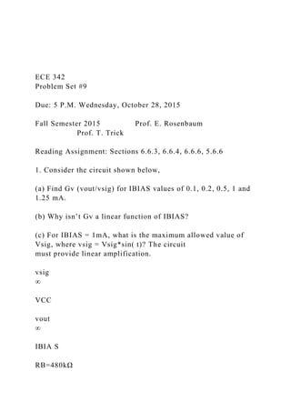
- 1. ECE 342 Problem Set #9 Due: 5 P.M. Wednesday, October 28, 2015 Fall Semester 2015 Prof. E. Rosenbaum Prof. T. Trick Reading Assignment: Sections 6.6.3, 6.6.4, 6.6.6, 5.6.6 1. Consider the circuit shown below, (a) Find Gv (vout/vsig) for IBIAS values of 0.1, 0.2, 0.5, 1 and 1.25 mA. (b) Why isn’t Gv a linear function of IBIAS? (c) For IBIAS = 1mA, what is the maximum allowed value of Vsig, where vsig = Vsig*sin( t)? The circuit must provide linear amplification. vsig ∞ VCC vout ∞ IBIA S RB=480kΩ
- 2. -VEE RL=100kΩ ∞ Rsig=10kΩ RC=10kΩ ß = 100 VA=25V 2. Consider the circuit shown below, (a) Choose the value of Re such that Gv is maximized, subject to the constraint that vbe ≤ 10mV and the transistor stays in the active mode. What is the value of Gv? (b) If β drops by 10%, what is the new value of Gv? All other design variables are unchanged. vsig=0.05sin(ωt) ∞ +5V vout ∞ 0.2mA 100kΩ
- 3. 20kΩ ∞ 20kΩ 20kΩ ß = 100 VA=∞ Re -5V 10V -10V 3. Find Rin, Rout, Gv, and the overall current gain io/isig (“Gi”). You are given that β=100 and VA=∞. VBE,ON = 0.7V. 100kΩ vsig ∞ 5V -5V 3.3kΩ 2kΩ
- 4. vo io ii 4. Choose the value of IBIAS such that vout is a sinusoidal signal with amplitude 200 mV or larger. 5V 10kΩ vout 75Ω ∞ vsig=0.5sin(ωt) VIN=3V IBIAS ß = 100 VA=∞ 5. Consider the circuit shown below, (a) Find the dc bias point and small-signal model parameters. Assume λ = 0.
- 5. (b) Find Rin, Rout, Avo and Gv. (c) Repeat part (b) for the case that λ = 0.03. You will have to recalculate ro. (d) Finally, you will consider the body effect; i.e., you will no longer assume that V B = VS but, instead, that VB = -VSS, which is -5V in this circuit. You are given γ = 0.4V 1/2 and 2ϕF = 0.6V. You may assume λ = 0 for simplicity. First, you need to recalculate the dc bias point. You may iteratively solve for VS and Vt, using ( ) and (√ √ ). Do not iterate more than 2 or 3 times, as this should be sufficient to obtain the value of V t with less than 10mV error. Then, redraw the small-signal model, now including the gmb current source shown in Fig. 5.62 of the textbook. The value of gmb can be found using equations (5.110) and (5.111). You are to calculate the value of Gv. 1MΩ
- 6. vsig ∞ 5V 5kΩ vout 4.7MΩ -5V ∞ 0.5mA Vto=0.75V k=2mA/V 2 ENSC 324 HOMEWORK #2 Fall 2015 DUE: Monday October 19, 2015 at 2 PM (note new time!) Please note that unless you show work in the derivations and solutions you will get no credit for the answers. Obviously copied answers from study partners or other
- 7. sources, etc., will also receive no credit. Please do all parts of all eight problems. It is suggested that you make a copy of your homework before turning it in in case it cannot be returned before Exam 2 (solution key will be provided). Problem #1 In a particular sample of n-type silicon, the Fermi energy level varies linearly with distance over a short range. At x=0, the difference between the Fermi level and the intrinsic Fermi level is 0.4 eV. At x=10 -3 cm, the same difference is only 0.15eV. The electron diffusion coefficient is 25 cm 2 /s. a) Write an expression for the Fermi level with respect to the intrinsic fermi level versus distance. b) What is the electron concentration versus distance? c) What is the electron diffusion current density at x=0, and at x=5 x 10 −4 cm?
- 8. Problem #2 A rectangular bar shaped silicon semiconductor resistor with a cross-sectional area of 100 µm 2 , and a length of 0.1 cm, is doped with a concentration of 5 x 10 16 cm −3 arsenic atoms (and no acceptors). Let T = 300 K. A bias of 5V is applied across the length of the silicon resistor. a) Calculate the current in the resistor. b) Repeat part a) if the length is reduced by 0.01 cm. c) What is the drift current in parts a) and b)? Problem #3 Assume we have silicon with typical mid-range doping levels of donors (no acceptors) at 300K. Assume that the mobility for electrons is limited by lattice scattering and has a temperature dependence of approximately T -3/2
- 9. . Determine the electron mobility at: a) T=200K; b) 400K. Problem #4 A silicon bar has a length of L = 0.1 cm and a cross-sectional area of A = 10 −4 cm 2 . The semiconductor is uniformly doped with phosphorous at a level 5 x 10 16 cm −3 (no other doping). A voltage of 5 V is applied across the length of the material which is at T=300K. The minority carrier lifetime is 3 x 10 −7 s. For t < 0, the semiconductor has been uniformly illuminated with light, producing a uniform excess carrier generation rate of g' = 5 x 10 21 cm
- 10. −3 s −1 . At t = 0, the light source is turned off. Determine the current in the semiconductor as a function of time for -∞ ≥ t ≥ ∞. Problem #5 An n-type GaAs semiconductor at 300 K is uniformly doped with donors (no acceptors) at a level of 5 x 10 15 cm −3 (mid level doping). The minority carrier lifetime is 5 x 10 −8 s. A light source is turned on at t = 0 generating excess carriers uniformly at a rate of g' = 4 x 10 21 cm −3
- 11. s −1 . There is no external electric field. a) Determine the excess carrier concentrations versus time over the range 0 ≤ t ≤ ∞. b) Calculate the conductivity of the semiconductor versus time over the same time period as part (a). Problem #6 Consider a bar of p-type silicon material at T=300K that is homogeneously doped to a value of 3 x 10 15 cm −3 (ND=0), which may be considered mid level doping. The applied electric field is zero. A light source is incident on the end of the semiconductor on one end (where x = 0, with x increasing into the silicon bar). The excess carrier concentration generated at x = 0 is 10
- 12. 13 cm −3 . The lifetimes for electrons and holes are 0.5 µs and 0.1 µs, respectively. a) Calculate the steady-state excess electron and hole concentrations as a function of distance into the semiconductor. b) Calculate the electron diffusion current density as a function of x. Problem #7 Calculate the position of the quasi-Fermi level with respect to the intrinsic level for the following silicon crystal that is steadily illuminated with an excess carrier generation rate of 10 21 /cm 3 S: NA = 10 16 /cm 3
- 13. , ND = 0 τn0 = τp0 = 1 µS Problem #8 A silicon sample at 300K has the following impurity concentrations: ND = 10 15 /cm 3 and NA = 0 . The equilibrium recombination rate is Rp0 = 10 11 cm −3 s −1 . A uniform generation rate produces an excess carrier concentration of 10 14 /cm 3 . a) What is the excess carrier lifetime? b) By what factor does the total recombination rate increase?