1. 431 531 Class Notes 6
Following our discussion last time of the basic transistor switch and emitter follower, we
will likewise introduce the basic relations for two other transistor circuit con gurations: the
current source and the common-emitter ampli er. We will then return to the issue of input
and output impedance so that we can build realistic circuits using these con gurations.
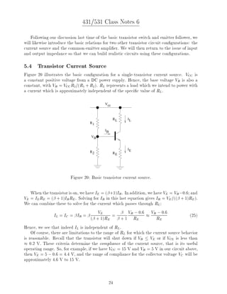
5.4 Transistor Current Source
Figure 20 illustrates the basic con guration for a single-transistor current source. VCC is
a constant positive voltage from a DC power supply. Hence, the base voltage VB is also a
constant, with VB = VCC R2=R1 + R2. RL represents a load which we intend to power with
a current which is approximately independent of the speci c value of RL.
Vcc
RL IL
R1
IB
VB
IE
R2 RE
Figure 20: Basic transistor current source.
When the transistor is on, we have IE = +1IB . In addition, we have VE = VB ,0:6; and
VE = IE RE = + 1IB RE . Solving for IB in this last equation gives IB = VE = + 1RE .
We can combine these to solve for the current which passes through RL:
IL = IC = IB =
VE ,
= + 1 VBR 0:6 VB R 0:6, 25
+ 1RE E E
Hence, we see that indeed IL is independent of RL.
Of course, there are limitations to the range of RL for which the current source behavior
is reasonable. Recall that the transistor will shut down if VB VE or if VCE is less than
0:2 V. These criteria determine the compliance of the current source, that is its useful
operating range. So, for example, if we have VCC = 15 V and VB = 5 V in our circuit above,
then VE = 5 , 0:6 = 4:4 V, and the range of compliance for the collector voltage VC will be
approximately 4:6 V to 15 V.
24
2. 5.5 Common-emitter Ampli er
Figure 21 represents the basic con guration of the common-emitter ampli er. To determine
the output for this circuit, we assume at this point that the input is a sum of a DC o set
voltage V0 and a time-varying signal vin, as discussed last time. In the next section we will
discuss how to achieve these. V0 provides the transistor bias, so that VB VE , and the
signal of interest is vin.
Vcc
RC
Vout
Vin
RE
Figure 21: Basic common-emitter ampli er.
The incoming signal shows up on the emitter: vin = VE + 0:6 = VE vE . And by
Ohm's Law, iE = vE =RE = vB =RE . As we found previously, iE = iC + iB iC . Now, the
voltage at the output is Vout = VC = VCC , IC RC . And therefore, Vout vout = ,iC RC .
Putting all of this together, vout = ,iC RC ,iE RC = ,vB =RE RC , giving the voltage
gain G:
G vout=vin = ,RC =RE 26
5.6 Circuit Biasing and Input
Now we need to gure out how to provide inputs to our basic circuits. In Fig. 22 below we
show the input network for a common-emitter ampli er. The same considerations we apply
here apply equally to the input of an emitter follower. The idea is that the voltage divider
R1 and R2 provide the DC bias voltage V0 in our discussion above, and the time varying
signal is input through the capacitor which blocks the DC. We need to gure out what
design criteria should be applied to this design.
We need to make sure that our input circuit does not load the ampli er, C is chosen
to give a reasonable RC cuto , and that the gain of the ampli er is what we want. We
will start by designing the DC component of the input network, that is choosing R1 and
R2 . It is helpful when designing the input network to consider the equivalent circuit shown
in Fig. 23. The diode and resistor labelled Zin represent the transistor input: the voltage
drop across the base-emitter diode and the input impedance from Eqn. 23. RTH is the
Thenenin equivalent resistance for the DC input network.
So our design procedure can be as follows:
25
3. Vcc
RC
R1
Vout
C
Vin
R2
RE
Figure 22: Common-emitter ampli er with input network.
R TH
VB
VTH IB
Z in
Figure 23: Equivalent circuit for design of DC input network.
1. Choose RTH Zin = RE + 1.
2. Determine R1 and R2 based on the equivalent circuit.
3. Choose C to provide a proper high-pass cuto frequency.
4. Choose the ampli er gain, if need be.
26