
Recommended
More Related Content
What's hot
What's hot (18)
Similar to 6 n137 datasheet_en_20170808 (1)
Similar to 6 n137 datasheet_en_20170808 (1) (20)
Recently uploaded
Recently uploaded (20)
6 n137 datasheet_en_20170808 (1)
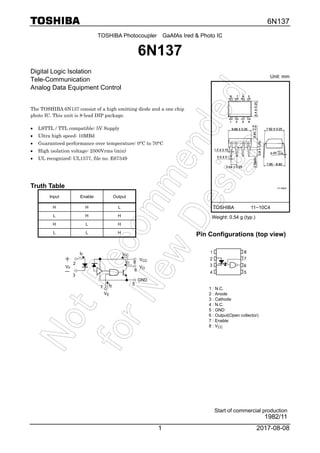
- 1. 6N137 2017-08-081 TOSHIBA Photocoupler GaAℓAs Ired & Photo IC 6N137 Digital Logic Isolation Tele-Communication Analog Data Equipment Control The TOSHIBA 6N137 consist of a high emitting diode and a one chip photo IC. This unit is 8-lead DIP package. • LSTTL / TTL compatible: 5V Supply • Ultra high speed: 10MBd • Guaranteed performance over temperature: 0°C to 70°C • High isolation voltage: 2500Vrms (min) • UL recognized: UL1577, file no. E67349 Truth Table Input Enable Output H H L L H H H L H L L H VCC VO VE GND ICC IE IO 7 IF VF 2 3 5 6 8 Pin Configurations (top view) 8 7 6 5 1 2 3 4 1 : N.C. 2 : Anode 3 : Cathode 4 : N.C. 5 : GND 6 : Output(Open collector) 7 : Enable 8 : VCC 8 Unit: mm TOSHIBA 11−10C4 Weight: 0.54 g (typ.) Start of commercial production 1982/11
- 2. 6N137 2017-08-082 Absolute Maximum Ratings Characteristic Symbol Rating Unit LED Forward current IF 20 mA Pulse forward current (Note 1) IFP 40 mA Reverse voltage VR 5 V Diode power dissipation PD 40 mW Input power dissipation derating (Ta ≥ 70 °C) △PD/°C -0.73 mW/°C Detector Output current IO 50 mA Output voltage VO 7 V Supply voltage (1 minute maximum) VCC 7 V Enable input voltage (not to exceed VCC by more than 500mV) VEH 5.5 V Output collector power dissipation PO 85 mW Output power dissipation derating (Ta ≥ 85 °C) △Po/°C -2.2 mW/°C Operating temperature range Topr 0 to 70 °C Storage temperature range Tstg −55 to 125 °C Lead solder temperature (10 s) (Note 2) Tsol 260 °C Note: Using continuously under heavy loads (e.g. the application of high temperature/current/voltage and the significant change in temperature, etc.) may cause this product to decrease in the reliability significantly even if the operating conditions (i.e. operating temperature/current/voltage, etc.) are within the absolute maximum ratings and the operating ranges. Please design the appropriate reliability upon reviewing the Toshiba Semiconductor Reliability Handbook (“Handling Precautions”/“Derating Concept and Methods”) and individual reliability data (i.e. reliability test report and estimated failure rate, etc.). Note 1: 50% duty cycle, 1ms pulse width. Note 2: Soldering portion of lead: Up to 2mm from the body of the device. Recommended Operating Conditions Characteristic Symbol Min Max Unit Input current, low level each channel IFL 0 250 μA Input current, high level each channel IFH 7 20 mA High level enable voltage VEH 2.0 VCC V Low level enable voltage (output high) VEL 0 0.8 V Supply voltage, output* VCC 4.5 5.5 V Fan out (TTL load) N ― 8 ― Operating temperature Ta 0 70 °C Note: Recommended operating conditions are given as a design guideline to obtain expected performance of the device. Additionally, each item is an independent guideline respectively. In developing designs using this product, please confirm specified characteristics shown in this document. *This item denotes operating ranges, not meaning of recommended operating conditions. Precaution Please be careful of the followings. A ceramic capacitor (0.1μF) should be connected from pin 8 to pin 5 to stabilize the operation of the high gain linear amplifier. Failure to provide the bypassing may impair the switching property. The total lead length between capacitor and coupler should not exceed 1cm.
- 3. 6N137 2017-08-083 Electrical Characteristics Over Recommended Temperature (Ta = 0 to 70°C unless otherwise noted) Characteristic Symbol Test Condition Min (**)Typ. Max Unit High level output current IOH VCC=5.5V, VO=5.5V IF=250μA, VE = 2.0V ― 1 250 μA Low level output voltage VOL VCC=5.5V, IF=5mA VEH=2.0V IOL(sinking)=13mA ― 0.4 0.6 V High level enable current IEH VCC=5.5V, VE=2.0V ― −1.0 ― mA Low level enable current IEL VCC=5.5V, VE=0.5V ― −1.6 −2.0 mA High level supply current ICCH VCC=5.5V, IF=0mA, VE=0.5V ― 7 15 mA Low level supply current ICCL VCC=5.5V, IF=10mA, VE=0.5V ― 12 18 mA Resistance (input−output) (Note 3) RI−O VI−O=500V, Ta=25°C R.H. ≤ 60% ― 1012 ― Ω Capacitance (input−output) (Note 3) CI−O f=1MHz, Ta=25°C ― 0.6 ― pF Input forward voltage VF IF=10mA, Ta=25°C ― 1.65 1.75 V Input reverse breakdown voltage BVR IR=10μA, Ta=25°C 5 ― ― V Input capacitance CIN VF=0V, f=1MHz ― 45 ― pF Current transfer ratio CTR IF=5.0mA, RL=100Ω ― 1000 ― % (**) All typical values are at VCC=5V, Ta=25°C Note 3: Pins 1, 2, 3 and 4 shorted together and pins 5, 6, 7 and 8 shorted together.
- 4. 6N137 2017-08-084 Switching Characteristics (Ta = 25°C, VCC = 5V) Characteristic Symbol Test Circuit Test Condition Min Typ. Max Unit Propagation delay time to high output level tpLH 1 RL=350Ω, CL=15pF IF=7.5mA ― 60 75 ns Propagation delay time to low output level tpHL 1 RL=350Ω, CL=15pF IF=7.5mA ― 60 75 ns Output rise−fall time (10−90%) tr, tf ― RL=350Ω, CL=15pF IF=7.5mA ― 30 ― ns Propagation delay time of enable from VEH to VEL tELH 2 RL=350Ω, CL=15pF IF=7.5mA VEH=3.0V VEL=0.5V ― 25 ― ns Propagation delay time of enable from VEL to VEH tEHL 2 RL=350Ω, CL=15pF IF=7.5mA VEH=3.0V VEL=0.5V ― 25 ― ns Common mode transient immunity at logic high output level CMH 3 VCM=10V RL=350Ω VO(min)=2V IF=0mA ― 200 ― V / μs Common mode transient Immunity at logic low output level CML 3 VCM=10V RL=350Ω VO(max)=0.8V IF=5mA ― −500 ― V / μs
- 5. 6N137 2017-08-085 Test Circuit 1. ・ CL is approximately 15pF which includes probe and stray wiring capacitance. Test Circuit 2. ・ CL is approximately 15pF which includes prove and stray wiring capacitance. Test Circuit 3. Transient immunity and typical waveforms VOL 350mV(IF = 7.5mA) Monitoring 175mV(IF = 3.75mA) VOH 7 8 6 7 5 6 1 5 2 1 3 2 4 3 8 5V CL By- pass VCC 47Ω IF Pulse generator ZO = 50Ω tr = 5ns Node RL Output VO monitor- ing node 0.1μF GND 1.5VOutput VO Input tpHL and tpLH tpHL tpLH VOL VOH 7.5mA IF dc Pulse generator ZO = 50Ω tr = 5ns CL By- pass RL Output monitoring node 0.1μF VO 7 8 6 7 5 6 1 5 2 1 3 2 4 3 8 5V VCC GND Input VE Monitoring node 3.0V 1.5V 1.5VOutput VO Input VE tEHL and tELH tEHL tELH VOL VO Switching at B : IF = 5mA 5V VO 0V tf 10% tr Switch at A : IF = 0mA 90% 90% 10% 10V 5V VO 7 8 6 7 5 6 1 5 2 1 3 2 4 3 8 By- pass VCC RL 0.1μF GND Pulse gen. ZO = 50Ω. VCM A VFF IF B
- 6. 6N137 2017-08-086 IF – VF Forward voltage VF (V) ForwardcurrentIF(mA) 0.01 100 1.0 10 1.2 1.4 1.6 1.8 1 0.1 Ta = 25°C ΔVF / ΔTa – IF Forward current IF (mA) Forwardvoltagetemperature coefficientΔVF/Δta(mV/°C) -1.6 -2.6 0.1 -2.4 -2.2 -2.0 -1.8 0.3 1 3 10 -1.4 30 IOH - Ta Ambient temperature Ta (°C) Highleveloutputcurrent IOH(μA) 10 3 0.5 0.3 806040200 0.1 1 5 VF = 1V VCC = 5.5V VO = 5.5V VO L – Ta Ambient temperature Ta (°C) 0 20 40 60 80 0.2 0.3 0.4 0.5 IF = 5mA VCC = 5.5V VE = 2V 12.8mA 9.6mA 6.4mA IOL = 16mA Lowleveloutputvoltage VOL(V) Forward current IF (mA) OutputvoltageVO(V) VO – IF 6543210 8 6 4 2 0 VCC = 5V RL = 350Ω RL = 4kΩ 0°C Ta = 70°C VO – IF Forward current IF (mA) OutputvoltageVO(V) 8 2 6 4 0 1 3 4 5 0 62 VCC = 5V Ta = 25°C RL = 350Ω 1kΩ 4kΩ
- 7. 6N137 2017-08-087 Ambient temperature Ta (°C) Propagationdelaytime tpHL,tpLH(ns) 120 0 80 60 40 20 10 20 30 40 50 0 60 VCC = 5V IF = 7.5mA 70 100 tpHL, tpLH - Ta tpLH tpLH tpHL 1kΩ 4kΩ 350Ω 1kΩ 350Ω RL = 4kΩ tr, tf – Ta Ambient temperature Ta (°C) Rise,falltimetr,tf(ns) 300 80 40 0 0 320 60 280 20 VCC = 5V IF = 7.5mA 10 20 30 40 50 60 70 RL = 4kΩ tf tf 1kΩ 350Ωtf tr 350Ω 1kΩ 4kΩ Ambient temperature Ta (°C) tEHL,tELH - Ta Enablepropagationdelaytime tEHL,tELH(ns) 7020 30 504010 60 80 70 60 50 40 30 20 10 0 0 VCC = 5V VEH = 3V IF = 7.5mA tEHL tELH tELH 1kΩ 350Ω 350Ω 1kΩ 4kΩ tELH RL = 4kΩ Propagationdelaytime tpHL,tpLH(ns) tpHL, tpLH - IF Forward current IF (mA) 120 100 17 19 20 0 151311975 40 80 60 Ta = 25°C VCC = 5V 350Ω 350Ω tpLH RL = 4kΩ tpLH 1kΩ tpHL tpLH 1kΩ 4kΩ
- 8. 6N137 2017-08-088 RESTRICTIONS ON PRODUCT USE Toshiba Corporation and its subsidiaries and affiliates are collectively referred to as “TOSHIBA”. Hardware, software and systems described in this document are collectively referred to as “Product”. • TOSHIBA reserves the right to make changes to the information in this document and related Product without notice. • This document and any information herein may not be reproduced without prior written permission from TOSHIBA. Even with TOSHIBA's written permission, reproduction is permissible only if reproduction is without alteration/omission. • Though TOSHIBA works continually to improve Product's quality and reliability, Product can malfunction or fail. Customers are responsible for complying with safety standards and for providing adequate designs and safeguards for their hardware, software and systems which minimize risk and avoid situations in which a malfunction or failure of Product could cause loss of human life, bodily injury or damage to property, including data loss or corruption. Before customers use the Product, create designs including the Product, or incorporate the Product into their own applications, customers must also refer to and comply with (a) the latest versions of all relevant TOSHIBA information, including without limitation, this document, the specifications, the data sheets and application notes for Product and the precautions and conditions set forth in the "TOSHIBA Semiconductor Reliability Handbook" and (b) the instructions for the application with which the Product will be used with or for. Customers are solely responsible for all aspects of their own product design or applications, including but not limited to (a) determining the appropriateness of the use of this Product in such design or applications; (b) evaluating and determining the applicability of any information contained in this document, or in charts, diagrams, programs, algorithms, sample application circuits, or any other referenced documents; and (c) validating all operating parameters for such designs and applications. TOSHIBA ASSUMES NO LIABILITY FOR CUSTOMERS' PRODUCT DESIGN OR APPLICATIONS. • PRODUCT IS NEITHER INTENDED NOR WARRANTED FOR USE IN EQUIPMENTS OR SYSTEMS THAT REQUIRE EXTRAORDINARILY HIGH LEVELS OF QUALITY AND/OR RELIABILITY, AND/OR A MALFUNCTION OR FAILURE OF WHICH MAY CAUSE LOSS OF HUMAN LIFE, BODILY INJURY, SERIOUS PROPERTY DAMAGE AND/OR SERIOUS PUBLIC IMPACT ("UNINTENDED USE"). Except for specific applications as expressly stated in this document, Unintended Use includes, without limitation, equipment used in nuclear facilities, equipment used in the aerospace industry, medical equipment, equipment used for automobiles, trains, ships and other transportation, traffic signaling equipment, equipment used to control combustions or explosions, safety devices, elevators and escalators, devices related to electric power, and equipment used in finance-related fields. IF YOU USE PRODUCT FOR UNINTENDED USE, TOSHIBA ASSUMES NO LIABILITY FOR PRODUCT. For details, please contact your TOSHIBA sales representative. • Do not disassemble, analyze, reverse-engineer, alter, modify, translate or copy Product, whether in whole or in part. • Product shall not be used for or incorporated into any products or systems whose manufacture, use, or sale is prohibited under any applicable laws or regulations. • The information contained herein is presented only as guidance for Product use. No responsibility is assumed by TOSHIBA for any infringement of patents or any other intellectual property rights of third parties that may result from the use of Product. No license to any intellectual property right is granted by this document, whether express or implied, by estoppel or otherwise. • ABSENT A WRITTEN SIGNED AGREEMENT, EXCEPT AS PROVIDED IN THE RELEVANT TERMS AND CONDITIONS OF SALE FOR PRODUCT, AND TO THE MAXIMUM EXTENT ALLOWABLE BY LAW, TOSHIBA (1) ASSUMES NO LIABILITY WHATSOEVER, INCLUDING WITHOUT LIMITATION, INDIRECT, CONSEQUENTIAL, SPECIAL, OR INCIDENTAL DAMAGES OR LOSS, INCLUDING WITHOUT LIMITATION, LOSS OF PROFITS, LOSS OF OPPORTUNITIES, BUSINESS INTERRUPTION AND LOSS OF DATA, AND (2) DISCLAIMS ANY AND ALL EXPRESS OR IMPLIED WARRANTIES AND CONDITIONS RELATED TO SALE, USE OF PRODUCT, OR INFORMATION, INCLUDING WARRANTIES OR CONDITIONS OF MERCHANTABILITY, FITNESS FOR A PARTICULAR PURPOSE, ACCURACY OF INFORMATION, OR NONINFRINGEMENT. • GaAs (Gallium Arsenide) is used in Product. GaAs is harmful to humans if consumed or absorbed, whether in the form of dust or vapor. Handle with care and do not break, cut, crush, grind, dissolve chemically or otherwise expose GaAs in Product. • Do not use or otherwise make available Product or related software or technology for any military purposes, including without limitation, for the design, development, use, stockpiling or manufacturing of nuclear, chemical, or biological weapons or missile technology products (mass destruction weapons). Product and related software and technology may be controlled under the applicable export laws and regulations including, without limitation, the Japanese Foreign Exchange and Foreign Trade Law and the U.S. Export Administration Regulations. Export and re-export of Product or related software or technology are strictly prohibited except in compliance with all applicable export laws and regulations. • Please contact your TOSHIBA sales representative for details as to environmental matters such as the RoHS compatibility of Product. Please use Product in compliance with all applicable laws and regulations that regulate the inclusion or use of controlled substances, including without limitation, the EU RoHS Directive. TOSHIBA ASSUMES NO LIABILITY FOR DAMAGES OR LOSSES OCCURRING AS A RESULT OF NONCOMPLIANCE WITH APPLICABLE LAWS AND REGULATIONS.