PCB Design Trends and Features
•Download as PPTX, PDF•
0 likes•336 views

This document discusses printed circuit board (PCB) design and how it has evolved with technology. It summarizes key features of PCB design software like schematic capture, layout, routing, and collaboration with 3D mechanical design tools. The software aims to improve design efficiency through reduced costs and time to market by integrating electronics and mechanical design, enabling real-time feedback and reducing errors. It also discusses how the software seamlessly connects PCB and 3D mechanical design within SOLIDWORKS for end-to-end product development.

Recommended
More Related Content
What's hot
What's hot (16)
Similar to PCB Design Trends and Features
Similar to PCB Design Trends and Features (20)
More from EGS Computers India Private Limited
More from EGS Computers India Private Limited (20)
Recently uploaded
Recently uploaded (20)
PCB Design Trends and Features
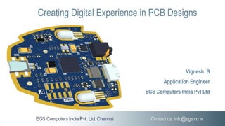
- 1. Vignesh B Application Engineer EGS Computers India Pvt Ltd Creating Digital Experience in PCB Designs
- 3. Electronic Industry - Recent Trends Electronics is everywhere Our customer’s design & manufacture millions of Electronic parts. Electro-mechanical Design integration is becoming critical. Electronic Market for Connected products is changing the industry.
- 4. Printed Circuit Boards PCB – The backbone of electrical & electronic devices. Non-conductive board - holds all the electronic components through a circuit embossed over it. Built for long last applications such as industrial and domestic products. Customized to any specifications to meet user’s requirements.
- 5. PCB - Parts ComponentsTop Layer Bottom Layer Traces Pads
- 7. PCB Designs aligned with Industry 4.0 Source : Parrot AR.Drone
- 8. Key Features Schematic Capture Traditional 2D PCB Layout 3D Visualization Layout Mechanical Collaboration SOLIDWORKS Ecosystem
- 9. Electronics Design Objectives Decreasing development costs Improving time to market
- 10. Schematic Capture Schematic Capture is the foremost step in the design cycle. This is done using intuitive tools and user interface. We can link the component to our supplier to see the component specification, price, and so on.
- 11. Schematic Capture Connection Matrix provides a mechanism to establish connectivity rules between component pins and net identifiers. Component you added in schematic readily capture in the BOM makes procurement easy and accurate.
- 12. E-Cad and M-Cad Design Collaboration PCB collaboration unifies design data and pushes changes to both sides of the design project. Managed ECAD-MCAD ECO Process takes care of design changes and keeps designs in sync. Real-Time 3D Clearance Checking ensure the board fit and component placement
- 13. Layer Stack Manager Layer stack manager allows the designer to configure and fully define the Layer Stack for the board design. A variety of layers can be included in the layer stack such as, • Copper • Dielectric • Surface Finish • Mask Layers
- 14. PCB Design Rule Editor DRC manager allows the designer to define the design rules for their requirement. Routing Widths Clearances Plane Connection Styles Routing Via Styles
- 15. Situs Auto Router This manager allows the designer to access a pre-routing setup report, and configure routing strategies. This uses advanced topological mapping to first define the routing path. A variety of proven routing algorithms are running back end to convert this 'human-like' path to a high-quality route.
- 16. Symbol Wizard Designer can quickly define the number of pins, the type of pin layout. Designer can change the information in the data grid by using simple commands like copy-paste. Using Pin layout style, component-style also can be modified like Dual in-line and quad side.
- 17. Benefits Unmatched ECAD-MCAD integration and collaboration Advanced Design Rule Checks Real Time Component Supplier Links Real-time Feedbacks Reduce Manual Errors UI Inspired by SolidWorks Powerful Unified Electronics Design Environment Integration of SolidWorks Models in the PCB Design Environment
- 18. Solutions Offered to PCB Designers Design and layout in one environment Real-time component supplier links ECAD-MCAD connection & collaboration SOLIDWORKS PCB costs < 1 prototype!
- 19. End to End Product Design Seamless Integration of Electronics into SOLIDWORKS Electrical & Mechanical Workflows SOLIDWORKS PCB SOLIDWORKS Electrical SOLIDWORKS Electrical 3D SOLIDWORKS
- 20. PCB Connector The SOLIDWORKS PCB Connector enables the designer to work on a seamless intelligent collaboration of ECAD-MCAD process between Altium Designer and SOLIDWORKS. Connector Easy Transition of Designs from Altium to SOLIDWORKS – thru PCB Connector. Connector
- 21. Chennai | Coimbatore | Trichy Thank You..! www.egsindia.com | www.egs.co.in bvignesh@egs.co.in 044 2480 3370