
Recommended
More Related Content
Similar to Nanochemistry Basics (B.Tech / B.E. ))
Similar to Nanochemistry Basics (B.Tech / B.E. )) (20)
Recently uploaded
Recently uploaded (20)
Nanochemistry Basics (B.Tech / B.E. ))
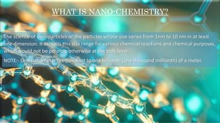
- 1. The science of nanoparticles or the particles whose size varies from 1nm to 10 nm in at least one dimension. It exploits this size range for various chemical reactions and chemical purposes, which would not be possible otherwise at the bulk level. NOTE:- One nanometer is equivalent to one billionth (one thousand millionth) of a meter. WHAT IS NANO-CHEMISTRY?
- 2. Properties of Nanomaterial The properties of nanomaterials are very different from those of the bulk material. The nanosize increases the surface area and has a marked effect on the electrical, electronic, optical and catalytic properties. Also new properties are introduced in the material. The other effects on the properties of nanomaterials are as follows: 1. Optical Properties This is markedly affected by the shape, size and surface characteristics, doping characteristics and environmental interactions of the nanoparticles. 2. Electrical Properties At nanoscale, the conductivity changes from metal to semiconductors to insulators, that is, from high to low. 3. Mechanical Properties They generally have good tensile strength, elasticity and fracture resistance. 4. Magnetic Properties Many substances which are non-magnetic in bulk become magnetic at the nanosize.
- 3. Self-Assembly Nanomaterials can be prepared either by dividing the bulky materials into small particles (top- down approach) or by assembling very small particles and binding them to size of 1–100 nm (bottom-up approach). Self-assembly is the basic principle underlying the bottom-up approach that helps to synthesize nanomaterials and enables them to organize into regular patterns with lowest energy configurations. It enables very small atoms to be arranged into ordered patterns to help them perform a particular function.
- 4. Principles of Self-Assembly 1. Components: The basic units that self-assemble to give patterned structures are the components. These components can be molecules or segments of macromolecules. 2. Interactions: The driving forces behind self-assembly are weak and non-covalent interactions such as Van Der Waals forces, electrostatic forces, hydrophobic interactions, - interactions, hydrogen bonds and coordination bonds. In self-assembly of larger objects of meso- and macro dimensions, other forces such as capillary forces, gravitational attractions, magnetic forces, electromagnetic interactions and entropic interactions also play a significant role. 3. Adjustability: It is essential that the forces between aggregates should be weak and easily disrupted by thermal motion. There is equilibria between the aggregated and non-aggregated states. 4. Environment: By modifying the environment (using boundaries and templates), the self-assembled structures can be tailored as per the requirement.
- 5. Types of Self-Assembly Self-assembly can be static or dynamic. Atomic and molecular crystals represent static assemblies. Examples of dynamic self-assemblies are solar system and galaxies. 1. Molecular Self-Assembly: Molecular self-assembly refers to the assembling of molecules without the aid of any external force. The molecules assemble spontaneously into stable and structured aggregates. The driving forces are reversible non-covalent interactions such as van der Waals forces, hydrogen bonds, - interactions, etc. Molecular self-assembly can be intermolecular as well as intramolecular. Molecular self-assembly actually refers to intramolecular self-assembly. 2. Material Self-Assembly: Material self-assembly results from the assembling of various nanosized blocks. In these lattices, the atoms of conventional solids are replaced by nanomaterials. In material self-assembly, the organic, inorganic and polymeric chemical components with well defined functions integrate into electronic, photonic, mechanical, analytical and chemical systems for an intended nanotechnological application.
- 6. Self-Assembling Materials 1. Ultrathin Film It is a 1-Å-thick film of atom spread on a flat surface. It is produced by the vaporization and subsequent deposition of atoms on a solid substrate. This technique that produces one-atom-thick layers is called the atomic layer deposition. 2. Langmuir-Blodgett (LB) Film A dilute solution of amphiphilic molecules (molecules having both water-loving and water-hating parts) spread on the surface of water. These molecules do not dissolve in water and when the solvent sticking to them evaporates they are left floating at the water–air interface and organize into a one-molecule-thick layer (monolayer), two- molecule-thick layer (bilayer) or several-molecule-thick layer (multilayer) 3. Self-Assembled Monolayer (SAM) It is formed by the adsorption of an active surfactant on a solid surface. An SAM film can be deposited by vapor phase deposition. The formation of SAMs does not require the application of external pressure. 4. Mesoscale Self-Assembly (MESA) The size of mesoscale self-assembly (MESA) varies from 10 nm to 10 mm (1cm). The components of MESA are bigger than molecules; hence, apart from the forces employed in molecular self-assembly they can utilize a wide range of other interactions such as capillary, electrostatic, magnetic, optical, gravitational and fluidic sheer.
- 7. Molecular vs Mesoscale Self-Assembly
- 8. Preparation of Nanomaterials Nanomaterials can be synthesised in a number of ways. The various methods generally employed for the synthesis of nanomaterials are as follows: 1. Mechanical Grinding 2. Wet Chemicals Synthesis 3. Gas Phase Synthesis
- 9. 1. Mechanical Grinding: This method of synthesis of nanomaterials follows a top-down approach. In this method, the nanoparticles are not synthesised by assembling small particles but by the structural decomposition of larger particles by the use of mechanical mills. This method is simple and inexpensive but causes environmental pollution. 2. Wet Chemical Synthesis: Wet synthesis can follow the top-down approach in which a single crystal is etched into nano- sized particles in aqueous solution. Porous silicon is synthesized by electrochemical etching. It can also follow a bottom-up approach where small particles agglomerate in a controlled manner to form nanosized particles.
- 10. 3. Gas-Phase Synthesis: Gas–phase synthesis is gaining importance as they have certain advantages such as, the size, shape and chemical composition of the nanomaterials can easily be controlled, substances formed are of high purity and the reaction mechanism is easily controllable. The conventional gas phase synthesis is the chemical vapor deposition (CVD) method in which small clusters of nanoparticles are produced because of condensation. CVD can be achieved in a number of ways:- (a). Furnace Heating- The appropriate material is heated in a furnace upto a temperature of 2000 °C. The material is evaporated in an inert atmosphere. The hot particles are then condensed into small clusters. The size is controlled by removing them rapidly from the supersaturated region with the help of a carrier gas. (b). Flame-Assisted Ultrasonic Spray Pyrolysis- In this method the precursor is nebulised to obtain its vapors which are then pyrolysed by burning in an acetylene oxygen flame or hydrogen oxygen flame.
- 11. (c). Gas Condensation Processing (GPC)- The desired substance is vaporized by thermal evaporation or by sputtering in an inert atmosphere of He, Ne, Ar and Kr or by a laser beam. The particles are then condensed and collected either in a solvent or by deposition on a collection device. This method helps in the synthesis of pure nanocrystalline substances. (d). Chemical Vapor Condensation (CVC)- In this method the source of evaporation is replaced by a hot wall reactor. The vapors of precursor are introduced into the hot wall reactor, where, by adjusting the conditions, nano-sized clusters are formed that are condensed and removed. This method is useful for the synthesis of nanoparticles of nitrides & carbides. CVC GPC
- 12. (e). Sputtered Plasma Processing- This method is similar to the gas phase condensation method, except that the precursor is sputtered using rare gases and then the particles agglomerate to produce nanomaterials. (f). Microwave Plasma Processing- In this technique the precursor is vaporised using plasma instead of high temperature. In this method, the precursor is introduced from the front of the reaction vessel that is made of quartz and is placed in a cavity connected to a microwave generator. The advantage of plasma- assisted pyrolysis is that the precursor can be activated at low temperatures that prevent the excessive agglomeration of the primary particles. SPP MPP
- 13. Nanomaterials Nanomaterials form the basis of nanoscience and nanotechnology. They are very small materials with the particle size ranging from 1 to 100 nm. The different types of nanomaterials are as follows: 1. Carbon Nanotubes 2. Nanocrystals 3. Quantum Dots 4. Nanowire 5. Carbon Nanocones 6. Haeckalites
- 14. 1. Carbon Nanotubes Carbon nanotubes are considered as allotropes of carbon belonging to the fullerene family. A carbon nanotube consists of a sheet of carbon atoms that are sp2-hybridised and have a hexagonal symmetry. Such a two-dimensional sheet is called graphene. A carbon nanotube is produced by rolling a graphene sheet into a cylindrical shape. Since its length is several times the width and the l/d ratio is of the order 100, hence CNTs are considered as 1-D structures. Types of Carbon Nanotubes: (i). Single Walled Nanotube (SWNT) – Consists of one single tube. (ii). Multi-Walled Nanotube (MWNT) – Consists of several concentric tubes aligning themselves through non-bonding interactions such as vander waals forces, pi stacking. SWNT MWNT
- 15. 2. Nanocrystals A nanocrystal is an inorganic entity in which the constituent atoms or ions have a crystalline arrangement in at least one dimension and their size is less than 100 nm. Semiconductor nanocrystals with size <10 nm are termed as ‘quantum dots’. Nanocrystals can be synthesised from vapor phase by crystallisation on substrate through heterogeneous nucleation or by controlled homogeneous nucleation in a super- saturated liquid phase. The agglomeration of the nanocrystal is prevented by capping them with suitable capping or protecting agents. The nanocrystals link molecules and bulk materials. Their properties depend strongly on their dimension and change continuously as a function of their size.
- 16. 3. Quantum Dots Quantum dots are nanoparticles that range from 2 to 10 nm in diameter and are made strictly from semiconductor materials. They can be prepared both by the top-down approach and the bottom-up approach. The top-down approach includes milling and grinding, whereas in the bottom-up approach one can use gas phase or liquid state approaches. The size and structure of the quantum dots can be carefully controlled. Properties: The optical properties of quantum dots are affected by the nature and area of the surface. Their properties change significantly when an electron leaves the surface. Quantum dots emit photons under excitation and these are visible to the human eye as light. By controlling their size, it is possible to monitor their wavelength of emission and this in turn determines the color of light perceived by the human eye.
- 17. 4. Nanowire Nanowires have diameter of the order of a nanometre (10−9 m) and their length-to-width ratio is greater than 1000; hence, they are also referred to as a one-dimensional material. They can be of various types: (i). Metallic (e.g., Ni, Pt and Au). (ii). Semiconducting (e.g., silicon. gallium nitride and indium phosphide). (iii). Insulating (e.g., Si𝑂2 and Ti𝑂2). (iv). Molecules that have repeating molecular units. They can be organic (DNA) or inorganic (M𝑜6𝑆9−𝑥𝐼𝑥). Nanowires behave like ballistic conductors. In normal conductors, the speed of the conducting electrons reduces because of collision with atoms, whereas in ballistic conductors electrons travel through the conductor without colliding with the atoms. Nanowires can conduct efficiently without heating the conductor wire.
- 18. 5. Carbon Nanocones Also known as ‘Nanohorns’, they are conical structures made of carbon with one nanometer diameter at least in one dimension. Unlike nanowires, the height and base diameter in nanocones is the same. The single-walled carbon nanohorns (SWNH) form one class of such conical structure with a sharp apical angle. Carbon nanocones are produced by the pyrolysis of heavy oil with a plasma torch having temperature above 2000 °C. Nanowires find use in the photovoltaic industry. Nanocones, because of their shape, enhance the absorption of light and reduce scattering and reflection of light. This helps in the production of economically viable photovoltaic devices.
- 19. 6. Haeckalite Haeckalites, named in the honour of the nineteenth century German zoologist Ernst Haeckel, consist of a layered structure of pentagons, hexagons and heptagons. They can also be rolled like carbon nanotubes to give tubular structures. In the rolled structures, the bands of heptagons have a negative curvature and bands of pentagons have a positive curvature. The haeckalite nanotubes may have different structures such as nanocoils, string of pearls, corrugated cylinders, etc. The stiffness and Young’s modulus of haeckalites is of the same order of classical carbon nanotubes. Haeckalites find application in lithium storage, hydrogen storage, electronic devices, in the medical field, manufacture of sensors, etc.
- 20. Characterization of nanomaterials helps in understanding the physical and chemical properties of nano-materials. It also helps in determining the structure at atomic and microscopic levels. Bulk properties like shape, size, phase, electronic structure and crystallinity and surface properties like arrangement of surface atoms, surface area, surface composition and surface electronic structure are determined by the various characterization techniques. The commonly used techniques are Brunauer–Emmet– Teller (BET) surface area analysis, Fourier transform infrared spectroscopy (FTIR), transmission electron microscopy (TEM), scanning electron microscopy (SEM), etc. Characterization of Nanomaterials
- 21. 1. BET surface area analysis: This is done by gas sorption method. Prior to determination the adsorbed foreign particles are removed from the surface of the adsorbent by heating and degassing by vacuum force. Sometimes instead of subjecting the adsorbent to vacuum force it is cleaned by flushing the adsorbent with an inert gas at elevated temperature. After cleaning the sample is brought to a constant and very low temperature usually in a dewar flask containing liquid nitrogen (77.4 K). Controlled doses of adsorbate gases are admitted into the evacuated sample chamber. They are first adsorbed and then desorbed. Adsorption and desorption isotherms are obtained by subjecting the gas to a wide range of pressures. By knowing the area occupied by one adsorbate molecule the total surface area can be determined using the adsorption model. 2. TEM : This technique is used for the structural information of solid material both by imaging and by electron diffraction. a thin specimen is irradiated with an electron beam of uniform current density; the electron density is in the range of 60–150 (usually 100 keV). For high-resolution TEM (HRTEM) or high voltage electron microscope HVEM the electron density of 200 keV–1MeV is used. The electrons emitted from the electron gun by thermionic emission from tungsten cathodes or La𝐵6 rods enter the sample and are scattered as they pass through it. They are then focused by the objective lens and amplified by the magnifying projector to produce the desired image. It causes complex absorption and scattering effects leading to the spatial variation in the intensity of the transmitted electrons.
- 22. Applications of Nanomaterials 1. Medicine: Nanomaterials are used in medicine as drug carriers. Their large surface area enables them to load the drug on them and their small size helps them to transport these drugs into the cells, nuclei and across the membranes. 2. Catalysis: The nanoparticles have large surface area and hence provide higher catalytic activity. This property finds use in catalysis by precious metals such as Pd, Pt and Rh. These metals are widely used as catalysts but they are very expensive. The nano size of these catalysts increases the reactive surface area, making them extremely active and thereby economizing their use. 3. Environmental Technologies: Nanoparticles on powder supports or on tubular monoliths form a catalytic system used widely in the removal of pollutants such as oxidation of volatile organic compounds (VOCs) in chimneys. 4. Electronics: Use of nanomaterials helps in reducing the size of these gadgets. The properties of particles of nano-dimensions are used to develop sensors whose functional units are nano-entities, although the material itself is not nano in dimension. The high surface-to-volume ratio of nanomaterials, their optical, electrical and physical properties help them initiate response to the minute change in the concentration of the species to be detected.
- 23. THANK YOU!