1. HIGHLY CONCENTRATED SILVER DISPERSIONS FOR ULTRA-LOW TEMPERATURE
PRINTABLE ELECTRONICS
Dr. Ajeet Kumar and Dr. Dan V. Goia, E-mail: goiadanv@clarkson.edu, ajkumar@clarkson.edu.
Chemistry & Biomolecular Science, Clarkson University, Potsdam, New York, USA
RESEARCH CHALLENGES AND
OBJECTIVES
PARTICLES SYNTHESIS
CONCLUSIONSCONCLUSIONS
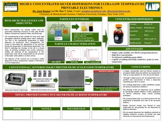
• Silver nanoparticles are already widely used for
generating conducting structures in solar cells, flexible
displays, transparent conductive films, and RFID tags.
• The manufacturing of inks suitable for large scale, high
throughput industrial printing posses many challenges.
The first is the reproducible preparation of highly
dispersed yet inexpensive silver nanoparticles. The
second is preventing the aggregation of the particles
during the preparation of concentrated dispersions. The
third is adjusting the rheology of the ink to a broad
range of printing techniques and various substrates.
Finally, the sintering of the nanoparticles at low
temperature must not be compromised by the presence
of thermally stable additives on their surface.
• The objective of the research was to develop a stable
dispersion of silver nanoparticles capable of sintering at
very low temperature.
CONCENTRATED DISPERSION
Viscosity 250-300 cP
Surface Tension 35-40 dyne/cm
Ag content ~ 60% (w/w)
Solvent Water
Zeta potential -25mV @ pH 7.0
Specific gravity 1.54 g/cm3
NOVEL: PRINTED CONDUCTIVE SILVER FILMS AT ROOM TEMPERATURE
0 10 20 30 40 50 60 70 80 90 100
0
10
20
30
40
50
60
70
Intensity(a.u.)
Diameter (nm)
Mean diameter = 12.5 nm
FE-SEM
• A simple, reproducible, and cost effective method to
precipitate highly dispersed uniform Ag nanoparticles
with an average diameter of 10±2 nm was developed.
• Through a simple process, the Ag nanoparticles were
purified and concentrated to form a dispersion
containing up to 60 wt.% metal.
• The resulting dispersion is stable indefinitely despite
the absence of polymeric stabilizers.
• The rheology of the raw dispersion can be modified
by introducing suitable additives to allow application
on diverse substrates using various printing
techniques.
• The prepared dispersion is an ideal precursor for the
preparation of printable silver inks in the electronic
industry.
• Simple electrical circuits were formed at room
temperature by ‘pen-printing’ the raw dispersion on
different substrates.
• The developed dispersion has significant potential in
building conductive circuitry on flexible and rigid
substrates at room and elevated temperatures.
UV-Vis DLS ANALYSIS
FE-SEM
PARTICLE CHARACTERIZATION
- Uniform Ag nanoparticles
- Highly dispersed
- 10±2 nm average diameter
- No polymeric capping agent
• Simple, easily scalable, cost effective preparation process
• High silver concentration.
• No polymeric stabilizing agent added.
• Capable of yielding electrically conductive prints at room
temperature.
ADVANTAGES
400 600 800 1000 1200
0.0
0.2
0.4
0.6
0.8
1.0
Intensity(a.u.)
Wavelength (nm)
404 nm
CONVENTIONAL: SINTERED INKJET PRINTED FILMS AT ELEVATED TEMPERATURE
TOP VIEW OF Ag FILM ON GLASS AS
PRINTEDDIMATIX INKJET PRINTER
PRINTED PATTERN ON
POLYMER FILM
TOP VIEW OF Ag FILM ON GLASS
AFTER SINTERINGPRINTED PATTERN ON GLASS
140ºC
20 min.
PAPER TEXTILE POLYMER FILM GLASS
(Resistivity=6µΩcm)