SPICE MODEL of TC7WH02FK in SPICE PARK
•
0 likes•122 views

This document summarizes the testing and simulation of a CMOS digital integrated circuit. It includes truth tables, circuit diagrams, timing diagrams, and comparison tables for input/output voltages and propagation delay times between measurement and simulation results. Minor differences within a few percent were observed between measured and simulated values.

Recommended
Recommended
More Related Content
What's hot
What's hot (20)
Similar to SPICE MODEL of TC7WH02FK in SPICE PARK
Similar to SPICE MODEL of TC7WH02FK in SPICE PARK (16)
More from Tsuyoshi Horigome
More from Tsuyoshi Horigome (20)
Recently uploaded
Recently uploaded (20)
SPICE MODEL of TC7WH02FK in SPICE PARK
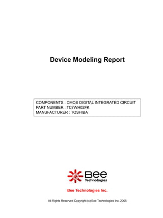
- 1. Device Modeling Report COMPONENTS : CMOS DIGITAL INTEGRATED CIRCUIT PART NUMBER : TC7WH02FK MANUFACTURER : TOSHIBA Bee Technologies Inc. All Rights Reserved Copyright (c) Bee Technologies Inc. 2005
- 2. Truth Table Circuit simulation result U1:1A 0 U1:1B 0 U1:2A 0 U1:2B 0 Y1 1 Y2 1 0s 0.5us 1.0us Time Evaluation circuit U1 LO 1A VCC 1B 1Y LO Y1 2Y 2B Y2 LO GND 2A LO R1 V1 TC7WH02 1MEG 5 0 Comparison table Input Output %Error An Bn Yn (Measurement) Yn (Simulation) L L H H 0 All Rights Reserved Copyright (c) Bee Technologies Inc. 2005
- 3. Truth Table Circuit simulation result U1:1A 0 U1:1B 1 U1:2A 0 U1:2B 1 Y1 0 Y2 0 0s 0.5us 1.0us Time Evaluation circuit U1 LO 1A VCC HI 1B 1Y Y1 2Y 2B HI Y2 GND 2A LO R1 V1 TC7WH02 1MEG 5 0 Comparison table Input Output %Error An Bn Yn (Measurement) Yn (Simulation) L H L L 0 All Rights Reserved Copyright (c) Bee Technologies Inc. 2005
- 4. Truth Table Circuit simulation result U1:1A 1 U1:1B 0 U1:2A 1 U1:2B 0 Y1 0 Y2 0 0s 0.5us 1.0us Time Evaluation circuit U1 HI 1A VCC 1B 1Y LO Y1 2Y 2B Y2 LO GND 2A HI R1 V1 TC7WH02 1MEG 5 0 Comparison table Input Output %Error An Bn Yn (Measurement) Yn (Simulation) H L L L 0 All Rights Reserved Copyright (c) Bee Technologies Inc. 2005
- 5. Truth Table Circuit simulation result U1:1A 1 U1:1B 1 U1:2A 1 U1:2B 1 Y1 0 Y2 0 0s 0.5us 1.0us Time Evaluation circuit U1 HI 1A VCC HI 1B 1Y Y1 2Y 2B HI Y2 GND 2A HI R1 V1 TC7WH02 1MEG 5 0 Comparison table Input Output %Error An Bn Yn (Measurement) Yn (Simulation) H H L L 0 All Rights Reserved Copyright (c) Bee Technologies Inc. 2005
- 6. High Level and Low Level Input Voltage Circuit simulation result 5.0V Output 2.5V Input 0V 0s 1.0ms 2.0ms 3.0ms 4.0ms V(R1:1) V(V1:+) Time Evaluation circuit U1 1A VCC LO 1B 1Y 2Y 2B GND 2A V1 V1 = 0 R1 V2 V2 = 5 TC7WH02 TD = 0.5m 1MEG TR = 0.1m 5 TF = 0.1m PW = 1m PER = 2m 0 Comparison table VCC = 5V Measurement Simulation %Error Min VIH = (VCC*0.7) (V) 3.5 3.6252 3.577 Min VIL = (VCC*0.3) (V) 1.5 1.4951 -0.327 All Rights Reserved Copyright (c) Bee Technologies Inc. 2005
- 7. High Level and Low Level Output Voltage Circuit simulation result 5.0V 2.5V Output 0V V(R1:1) Input 5.0V 2.5V SEL>> 0V 0s 5ms 10ms V(V1:+) Time Evaluation circuit U1 1A VCC LO 1B 1Y 2Y 2B GND 2A V1 V2 V1 = 0 R1 V2 = 4.5 TC7WH02 TD = 0.5m 1MEG 4.5 TR = 3n TF = 3n PW = 1m PER = 2m 0 Comparison table VCC = 4.5V Measurement Simulation %Error VOH (V) 4.5 4.4965 -0.078 VOL (V) 0 0 0 All Rights Reserved Copyright (c) Bee Technologies Inc. 2005
- 8. Propagation Delay Time Circuit simulation result 5.0V Output 2.5V Input 0V 0s 50ns 100ns V(U1:1Y) V(V1:+) Time Evaluation circuit U1 1A VCC LO 1B 1Y 2Y 2B GND 2A V1 V2 V1 = 0 C1 TC7WH02 V2 = 5 TD = 10n 15p 5 TR = 3n TF = 3n PW = 50n PER = 100n 0 Comparison table CL=15pF,VCC=5V,Tr=Tf=3ns Measurement Simulation %Error tpLH (ns) 3.6 3.6561 1.558 tpHL (ns) 3.6 3.6664 1.844 All Rights Reserved Copyright (c) Bee Technologies Inc. 2005