
Recommended
More Related Content
What's hot
What's hot (18)
Similar to Data and Power Flow in Circuits and the Origin of Electromagnetic Interference
Similar to Data and Power Flow in Circuits and the Origin of Electromagnetic Interference (20)
Recently uploaded
Recently uploaded (20)
Data and Power Flow in Circuits and the Origin of Electromagnetic Interference
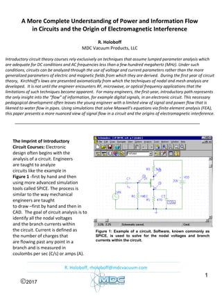
- 1. 1 A More Complete Understanding of Power and Information Flow in Circuits and the Origin of Electromagnetic Interference R. Holoboff MDC Vacuum Products, LLC Introductory circuit theory courses rely exclusively on techniques that assume lumped parameter analysis which are adequate for DC conditions and AC frequencies less than a few hundred megahertz (MHz). Under such conditions, circuits can be analyzed through the use of voltage and current parameters rather than the more generalized parameters of electric and magnetic fields from which they are derived. During the first year of circuit theory, Kirchhoff’s laws are presented axiomatically from which the techniques of nodal and mesh analysis are developed. It is not until the engineer encounters RF, microwave, or optical frequency applications that the limitations of such techniques become apparent. For many engineers, the first-year, introductory path represents the only insight into the “flow” of information, for example digital signals, in an electronic circuit. This necessary pedagogical development often leaves the young engineer with a limited view of signal and power flow that is likened to water flow in pipes. Using simulations that solve Maxwell’s equations via finite element analysis (FEA), this paper presents a more nuanced view of signal flow in a circuit and the origins of electromagnetic interference. The Imprint of Introductory Circuit Courses: Electronic design often begins with the analysis of a circuit. Engineers are taught to analyze circuits like the example in Figure 1 -first by hand and then using more advanced simulation tools called SPICE. The process is similar to the way mechanical engineers are taught to draw –first by hand and then in CAD. The goal of circuit analysis is to identify all the nodal voltages and the branch currents within the circuit. Current is defined as the number of charges that are flowing past any point in a branch and is measured in coulombs per sec (C/s) or amps (A). Figure 1: Example of a circuit. Software, known commonly as SPICE, is used to solve for the nodal voltages and branch currents within the circuit. ©2017 R. Holoboff, rholoboff@mdcvacuum.com
- 2. 2 Students are told that these charges are in fact subatomic particles called electrons. By convention it is assumed the charge is negative with a measured value of about -1.602 10^-19 C. So a modest 10 mA current is equivalent to about 10^16 (about 10 million billion) electrons passing a given point in the circuit each second. Another convention, one dating back to Ben Franklin, ignores the electron and assumes that current is the net flow of positive charge carriers. Electron flow is simply in the opposite direction of the calculated and assumed positively charged current. Voltage (or potential difference) is defined as the energy needed to move a unit charge from one point in the circuit to another. Often, voltage is explained away as the “pressure” that is required to move the charge carrier from one point to another. Thus, the connection between current flow in metal wires or printed circuit board conductors and the mechanical flow of water in pipes is established. As is customarily explained, voltage is the motive force that pushes pointlike charges, electrons specifically but imaginary point positive charges by convention, around the metal conductors of the circuit. Often, “current” becomes conflated with the mechanism by which information and power is transmitted in electrical or electronic circuits. For many problems this convenient shorthand is adequate. However, as we will soon see, this is a limited view of what is actually occurring. ©2017 Enter Kirchhoff: Circuit analysis relies on rules (Kirchhoff’s laws) to derive nodal voltages and branch currents. Kirchhoff’s laws may be derived from the more fundamental Maxwell’s equations. These laws are useful re-statements of the law of conservation of energy. Now, Kirchhoff’s laws may be applied in circumstances where the individual circuit elements can be considered “lumped parameters.” Circuit elements, for example resistors, inductors, capacitors, may be considered a lumped or discrete parameter when the voltage varies smoothly across the element. Figure 2: (A) Kirchhoff’s Current Law (KCL) and (B) Kirchhoff’s Voltage Law (KVL) KCL: The current going into a node is the same as the current leaving the node. KVL: The sum of the voltage changes around any closed loop is zero. Fig. 2 (A) Fig. 2 (B) node
- 3. 3 ©2017 In other words, the voltage changes in the circuit may be viewed as changing in discrete steps. For this to be true, the physical size of the resistor (or any element) must be small relative to the wavelength of the electrical energy exciting the circuit. Figure 3 shows this condition visually. Here we present a resistor whose physical size is less than 1/10 of the wavelength of the energy moving through the circuit. The result is that the voltage (vertical axis in Figure 3) changes smoothly and therefore we can assign a single value for the voltage change (drop) across the resistor. If the situation were reversed and the wavelength was 1000x smaller than the resistor, the voltage would be radically different at each point in the resistor. At some points it would be a maximum value and at other points it would be zero. In this instance, what value would we assign to the voltage change across the resistor? Engineers capture this Idea by saying the resistor is electrically small (relative to the wavelength). When the component or circuit is electrically small, the voltage variation (vertical displacement in Figure 3) is smooth and single- valued. Changes in voltage across the circuit may therefore be approximated as occurring in discrete steps. This approximation greatly simplifies the mathematical analysis and makes traditional circuit analysis (using Kirchhoff’s laws) possible. The Hydraulic Analogy: One consequence of this simplified approach is that it leads to a misunderstanding about how electromagnetic energy flows through the circuit. The simplification gives rise to the hydraulic analogy. The hydraulic analogy states that current within the circuit is due to microscopic particles (electrons) that flow through wires the same way water flows through pipes. The motive force propelling these particles is voltage –the analogue of pressure in the hydraulic case. Component is Electrically Small: L (length) << λ/10 Voltage (V) Time (s) λ Figure 3: The physical length of the resistor is small relative to the wavelength (λ) of energy exciting the circuit. This condition is referred to as being electrically small or electrically short. As a result, the voltage variation (the vertical change) across the component is small and therefore may be considered to occur in a discrete step.
- 4. 4 Figure 4: Electromagnetic energy flow in a PCB trace (horizontal and vertical views). Models created in ANSYS’ HFSS 3D electromagnetic (FEA) field solver simulator. This simplified model is accurate enough to design and build many practical circuits, but it is not generally correct. In Figure 4, we find a more accurate visualization of electromagnetic energy flow in a circuit. What is actually moving along the circuit trace is an electromagnetic field “disturbance.” What is being shown is the electric field component. (Now, a magnetic field is also present but, in most problems, its amplitude is so small in comparison to the electric field that its effects may be ignored.) As the field disturbance moves through the medium it pushes the electrons along with it –much like an ocean wave will push a cork as the wave passes. The electrons, however, do not translate very far before colliding with another electron. Hence, the net velocity of the electrons (the drift velocity) is very, very small when compared to the velocity the wave disturbance is moving along the circuit trace (i.e., at the speed of light). It is here the hydraulic analogy begins to fail. To be clear, it is the field disturbance that is moving at the speed of light in that medium along the wires or traces in any circuit. The Microstrip Model: Let’s unravel current flow in a PCB circuit trace a little further. In Figure 5 (A), we present a side view of the trace shown in Figure 4. The construction of the system is as follows. The top layer consists of the “wires” known as traces or microstrip lines. Traces are thin films of copper that are installed onto onto the PCB’s substrate or dielectric material. ©2017 Fig. 5 (A) Fig. 5 (B)Figure 5: Electric field coupling in a PCB microstrip FR4 FR4 FR4
- 5. 5 The Origin of Electromagnetic Interference (EMI): Traditional circuit analysis is valid when: • The circuit components are relatively small; • The circuit is switching slowly; or • The components are physically isolated from one another. If any of these assumptions fail or are invalid, then the “electromagnetic” behavior of the component or circuit must be taken into account. Traditional circuit analysis, involving currents and voltages, will not provide adequate explanations of the circuit’s behavior. An example of a component where these assumptions are no longer valid is a spiral inductor. Spiral inductors are used to control current in oscillating circuits and may be found in most RF or radio electronic systems. For example, every cell phone has several of these devices. These components are large relative to the MHz or GHz frequencies being used, are experiencing high switching rates, and have coils that are very close to another so that electromagnetic coupling may be occurring between the coils. In Figure 6, we see an example of the energy flow along a spiral. The FEA animation makes several “real world” features apparent. First, note how the color changes as the field travels along the spiral path. This is capturing the effect of the energy attenuation as the field progresses. No real system is perfectly frictionless; there always is an energy penalty. Second, note the presence of a reflected wave at the input port. Reflections often occur at boundaries when material impedances are likely to change, too. A typical PBC dielectric material is FR4 –a glass reinforced epoxy-based laminate. The bottom layer is typically a copper ground plane. All electric fields begin and end on charge carriers. These carriers are electrons; however, by convention we consider current as being conducted by positive charge carriers. By another convention, it is assumed that the field is directed away from a positive charge carrier and is directed towards a negative charge carrier. The electric field lines shown in Figure 5 (B) are therefore for positive charge carriers. The field lines start from charge carriers in the copper traces and couple to separate charge carriers found in the copper ground plane. The field lines pass through and are concentrated in the dielectric substrate (FR4). The substrate is critical. It contains the bulk of the field disturbance and controls the speed of the bits (digital data) along the trace. What is shown in Fig. 4 is an animation constructed by solving Maxwell’s equations along the microstrip using finite element methods. As shown in Figure 4, the electric field disturbance moves along the trace. The colors show the field intensity falling off as one moves away from the trace. The models in Figures 4 and 5 are constructed with a dual microstrip trace. Two traces are used in most of today’s high speed computer and communication circuits. The digital signals in the dual traces are compared and used to ensure the correct data is sent between the transmitting and receiving integrated circuits (IC’s). If a bit error is detected (e.g., a zero is detected that should have been a one) the data is resent. That is, dual traces are used in a technique known as Hamming bit error detection and correction.
- 6. Business Confidential 6 Figure 6: Electromagnetic energy flow along a spiral inductor. The Virtues of Electromagnetic FEA Simulation: In Figure 4, we show an example of how energy flow through an electrical wire or circuit trace is always an electromagnetic event. In Figure 6, we show an example of a component whose behavior can only be captured through electromagnetic FEA simulation using electric field parameters rather than currents and voltages. With this component, the assumptions of circuit analysis break down and no longer apply. In the next example, we will motivate the origins of electromagnetic interference on a printed circuit board. In Figure 7, we have recreated the same example as in Figure 3 with one exception. In this example, we have removed a chunk of the ground plane and have replaced the FR4 with another dielectric -air. That is, we have two traces which are sitting on top of a hole. The PCB dielectric is hidden so that the model is visually less confusing. As before, we are injecting a signal into a dual microstrip trace and are simulating the flow of electromagnetic energy along the trace. In this instance, we are showing the radiation pattern on the ground plane –which now consists of copper and air. Now, circuit designers who are responsible for placing and routing components on a PCB know not to place a trace over a cut in the ground plane. Why? Two problems are likely to occur. First, because there is a boundary condition (i.e. an impedance) change where the copper ground plane meets the “air” of the cut, some of the incoming energy will get reflected back to the source. This results in less energy being transmitted across the trace. This effect is captured by the color change in the energy disturbance as it progresses from top to bottom. Second, the electric field itself has inertia and cannot easily navigate around the cut in the ground plane. ©2017
- 7. Business Confidential 7 Figure 7: Transmission lines over a split plane illustrate the 3D nature of electromagnetic problems. Attenuation due to impedance mismatch EMI radiation This is the same effect one experiences when traveling too fast around a cloverleaf on a highway. In this instance, the driver and passengers feel as if they are going to be thrown from the vehicle. In a similar fashion, the electric field has a difficult time remaining coupled between the copper signal trace and the copper ground plane. As a result, radiation begins to “peel away” from the circuit. This is the genesis of a troublesome phenomenon known as electromagnetic interference or EMI. Even simple traces are 3D structures. Traditional 2D circuit methods based on currents and voltages in nodes and branches cannot capture these effects. The only way to capture these effects is through more sophisticated, distributed element transmission line models or 3D FEA models that solve Maxwell’s equations directly. ©2017 Conclusions: Signal (power and information) flow in circuits, whether in electric power transmission lines or printed circuit board traces, is always and everywhere an electromagnetic field phenomenon. Such flow results from electric (electromagnetic) field disturbances moving through a dielectric (air, FR4). Under certain circumstances (electrically small circuits, low frequencies), simpler circuit models using only currents and voltages are adequate tools for analyzing and explaining circuit behavior. These simpler techniques tend to reinforce the hydraulic analogy to explain circuit behavior; while useful, the analogy is limited in the breadth of applications it can explain. For example, an analysis of the root causes of electromagnetic interference in a real circuit will often force the engineer to seek tools with a higher fidelity.