Detecting of NH3, CO2 polluted gases by using ZnO- In2O3 thin films
Richard Gaona Wafer Fabrication Work Sample
1. Introduction
Single
crystal
silicon
wafers
are
used
to
host
a
variety
of
microelectromechanical
structures
crafted
in
three
separate
modules.
The
first
pertains
to
surface
micromachining,
the
second
to
bulk
micromachining,
and
the
third
to
soft
lithography.
Module
one
demonstrates
the
construction
of
cantilever
beams
and
springs,
module
two
the
fabrication
of
thermal
actuators
and
a
wheatstone
bridge,
module
three
the
design
of
disposable
microfluidic
channels
with
biological
applications.
For
each
wafer
used,
additional
layers
are
deposited
on
top
for
structural
and
sacrificial
purposes.
In
module
one,
the
cantilever
beams
and
other
surface
machines
are
patterns
of
polySi
and
supported
by
the
sacrificial
SiO2
(see
Fig.
1).
(figure
1)
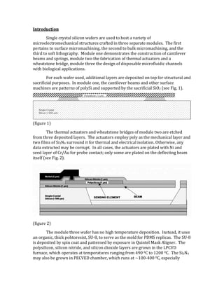
The
thermal
actuators
and
wheatstone
bridges
of
module
two
are
etched
from
three
deposited
layers.
The
actuators
employ
poly
as
the
mechanical
layer
and
two
films
of
Si3N4
surround
it
for
thermal
and
electrical
isolation.
Otherwise,
any
data
extracted
may
be
corrupt.
In
all
cases,
the
actuators
are
plated
with
Ni
and
seed
layer
of
Cr/Au
for
probe
contact;
only
some
are
plated
on
the
deflecting
beam
itself
(see
Fig.
2).
(figure
2)
The
module
three
wafer
has
no
high
temperature
deposition.
Instead,
it
uses
an
organic,
thick
pohtoresist,
SU-‐8,
to
serve
as
the
mold
for
PDMS
replicas.
The
SU-‐8
is
deposited
by
spin
coat
and
patterned
by
exposure
in
Quintel
Mask
Aligner.
The
polysilicon,
silicon
nitride,
and
silicon
dioxide
layers
are
grown
in
the
LPCVD
furnace,
which
operates
at
temperatures
ranging
from
490
0C
to
1200
0C.
The
Si3N4
may
also
be
grown
in
PECVED
chamber,
which
runs
at
~100-‐400
0C,
especially
2. when
the
thin
film
is
to
be
used
as
an
insulator
or
for
passivation.
The
Si3N4
used
here
is
deposited
by
LPCVD.
Additionally,
a
removable
layer
of
PR
is
commonly
used
throughout
fabrication
to
define
the
boundaries
of
etching.
In
the
first
module,
it
directs
HNA
removal
of
polysilicon,
in
the
second
it
demarcates
Si3N4
to
etch
and
where
to
apply
seed
layer
Cr/Au,
and
in
the
third
PR
is
a
structural
layer,
so
it
is
not
removed
after
patterning
as
in
the
first
two.
Layers
other
than
PR
are
measured,
grown,
and
etched
by
a
number
of
machines
in
the
lab.
Measurement
is
done
by
nanostep,
a
spectraphotometer
that
measures
intensity
of
reflected
light
at
different
wavelengths
to
calculate
thickness,
and
alphastep,
a
profilometer
that
registers
change
in
height
on
a
micrometer
scale
–
testing
is
carried
out
by
probe
station.
Oxide,
poly,
and
nitride
layers
are
all
deposited
by
LPCVD
(Low
Pressure
Chemical
Vapor
Deposition).
This
type
of
furnace
produces
conformal
films
at
high
temperatures
and
grows
poly
at
580-‐650
0C,
nitride
at
200-‐750
0C,
and
oxide
at
200-‐
900
0C,
depending
on
reactants
used.
Nickel
plating
is
done
by
electrodeposition
in
nickel
sulfate
solution,
the
wafer
connected
to
cathode
opposite
a
nickel
foil
anode.
Cr/Au
seed
layer
is
laid
by
CHA
e-‐beam
evaporator,
which
uses
accelerated
electrons
to
sublimate
metals.
Removal
of
these
layers
is
completed
with
Tegal
Plasma
Asher,
Oxford
Etcher,
and
STS
AOE
Etcher.
The
first
removes
unwanted
organic
material,
such
as
PR
residue,
with
O2
plasma;
the
second
two
are
for
nitride
etching.
The
STS
AOE
etches
nitride
in
module
two
using
a
voltage-‐biased
RF-‐generated
plasma
of
F2
and
O2.
This
machine
and
the
e-‐beam
evaporator
operate
under
high
vacuum
so
as
to
provide
a
sufficient
mean
free
path
for
impinging
atoms.
Additionally,
a
sonicator,
used
in
module
two,
removes
unwanted
Cr/Au
with
ultrasonic
pulses
in
an
acetone
bath.
Wet
chemicals
are
also
used
to
remove
specific
layers.
Piranha,
BOE
and
KOH
are
three
such
etchants
used
for
organic,
oxide,
and
silicon
removal,
respectively.
Two
other
machines
important
in
module
three
are
the
high
frequency
generator
and
volume
and
pressure
control
systems.
PDMA
mold
is
bonded
to
glass
with
O2
plasma
created
by
the
handheld
frequency
generator,
thus
making
the
microfluidic
channels.
The
volume
and
pressure
controllers,
equivalent
to
current
and
voltage
sources,
are
used
in
microfluidic
device
testing.
Water
is
flowed
through
the
channels
at
either
constant
volume
or
pressure.
Combined,
all
three
modules
provide
a
thorough
study
in
etching,
wet
and
dry,
PR
applications,
mask
alignment
and
design,
and
micromachine
measurement,
as
well
as
general
micromachine
design,
including
layer
optimization.
The
identifying
topics
of
each
stage
demonstrate
microscale
properties
of
mechanical,
electrical,
and
biological
nature.
3. Top
Views
and
Cross
Sections
Module
One
Thin-‐film
beams
are
patterned
to
demonstrate
the
effects
of
intrinsic
stress
and
surface
tension
on
surface
micromachines.
Lattice
mismatch
arises
from
the
characteristic
difference
between
the
geometry,
i.e.,
lattice
constants,
of
two
solid-‐state
crystal
materials.
Polysilicon
and
silicon
dioxide
experience
such
a
disparity,
creating
compressive
stress
on
the
poly,
and
the
result
is
a
buckling
effect
shown
in
figure
3.
Due
to
scaling
properties,
surface
tension
dominates
all
forces
on
a
micron
scale.
Volume
forces,
those
pertaining
to
mass,
and
surface
forces,
such
as
friction,
experience
a
higher
degree
of
reduction
when
an
object
becomes
smaller.
Line
forces,
such
as
surface
tension,
go
through
the
least
attenuation.
Therefore,
beams
and
sensors
may
be
stuck
to
the
wafer
surface
in
the
presence
of
liquid,
as
shown
in
figure
4.
After
etching
oxide
in
HF,
the
polysilicon
layer
is
measured
with
alphastep.
We
found
the
thickness
to
be
about
1
micron.
The
starting
and
final
wafers
are
shown
in
figure
5.
Buckling
can
be
seen
in
figure
6
on
the
190
and
180
micron
beams.
A
released
cantilevers
are
shown
in
figure
7.
(figure
3)
(figure
4
&
figure
5)