SlideShare a Scribd company logo
1 of 1
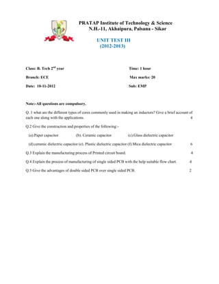
PRATAP Institute of Technology & Science
                                     N.H.-11, Akhaipura, Palsana - Sikar

                                              UNIT TEST III
                                               (2012-2013)


Class: B. Tech 2nd year                                             Time: 1 hour

Branch: ECE                                                         Max marks: 20

Date: 10-11-2012                                                    Sub: EMP


Note:-All questions are compulsory.

Q .1 what are the different types of cores commonly used in making an inductors? Give a brief account of
each one along with the applications.                                                                  4

Q.2 Give the construction and properties of the following:-

 (a).Paper capacitor            (b). Ceramic capacitor             (c).Glass dielectric capacitor

 (d).ceramic dielectric capacitor (e). Plastic dielectric capacitor (f).Mica dielectric capacitor     6

Q.3 Explain the manufacturing process of Printed circuit board.                                        4

Q.4 Explain the process of manufacturing of single sided PCB with the help suitable flow chart.       4

Q.5 Give the advantages of double sided PCB over single sided PCB.                                    2

More Related Content

Similar to Emp unit test 3

45nm transistor properties
45nm transistor properties45nm transistor properties
45nm transistor propertiesDeiptii Das
 
IRJET- Simulation of High K Dielectric MOS with HFo2 as a Gate Dielectric
IRJET-  	  Simulation of High K Dielectric MOS with HFo2 as a Gate DielectricIRJET-  	  Simulation of High K Dielectric MOS with HFo2 as a Gate Dielectric
IRJET- Simulation of High K Dielectric MOS with HFo2 as a Gate DielectricIRJET Journal
 
Performance analysis of high-k materials as stern layer in ion-sensitive fiel...
Performance analysis of high-k materials as stern layer in ion-sensitive fiel...Performance analysis of high-k materials as stern layer in ion-sensitive fiel...
Performance analysis of high-k materials as stern layer in ion-sensitive fiel...TELKOMNIKA JOURNAL
 
ECE499-Sp2016-tsai
ECE499-Sp2016-tsaiECE499-Sp2016-tsai
ECE499-Sp2016-tsaiPhilip Tsai
 
ECE499-Sp2016-tsai
ECE499-Sp2016-tsaiECE499-Sp2016-tsai
ECE499-Sp2016-tsaiPhilip Tsai
 
Seminar Report On O.L.E.D.
Seminar Report On O.L.E.D.Seminar Report On O.L.E.D.
Seminar Report On O.L.E.D.Sushant Shankar
 
THE EFFECT OF INTERFACE MODIFICATION BY PEDOT: PSS ON THE HOLE MOBILITY OF TH...
THE EFFECT OF INTERFACE MODIFICATION BY PEDOT: PSS ON THE HOLE MOBILITY OF TH...THE EFFECT OF INTERFACE MODIFICATION BY PEDOT: PSS ON THE HOLE MOBILITY OF TH...
THE EFFECT OF INTERFACE MODIFICATION BY PEDOT: PSS ON THE HOLE MOBILITY OF TH...ijoejournal
 
AC Lab Master Manual (2020-21).pdf
AC Lab Master Manual (2020-21).pdfAC Lab Master Manual (2020-21).pdf
AC Lab Master Manual (2020-21).pdfDrVikasMaheshwariECE
 
ITRI Jassy Wang
ITRI Jassy WangITRI Jassy Wang
ITRI Jassy Wangucsb.ira
 
The EM network October 2010 Newsletter
The EM network October 2010 NewsletterThe EM network October 2010 Newsletter
The EM network October 2010 Newsletterphovdenak
 
IRJET- Black Phosphorous as an Alternative to Current Semiconductor Materials
IRJET- Black Phosphorous as an Alternative to Current Semiconductor MaterialsIRJET- Black Phosphorous as an Alternative to Current Semiconductor Materials
IRJET- Black Phosphorous as an Alternative to Current Semiconductor MaterialsIRJET Journal
 
Jimmy Hsu English Resume
Jimmy Hsu English ResumeJimmy Hsu English Resume
Jimmy Hsu English ResumeJimmy Hsu
 
Le Van Hai- Resume
Le Van Hai- ResumeLe Van Hai- Resume
Le Van Hai- ResumeLe Hai
 

Similar to Emp unit test 3 (20)

45nm transistor properties
45nm transistor properties45nm transistor properties
45nm transistor properties
 
Tony
TonyTony
Tony
 
IRJET- Simulation of High K Dielectric MOS with HFo2 as a Gate Dielectric
IRJET-  	  Simulation of High K Dielectric MOS with HFo2 as a Gate DielectricIRJET-  	  Simulation of High K Dielectric MOS with HFo2 as a Gate Dielectric
IRJET- Simulation of High K Dielectric MOS with HFo2 as a Gate Dielectric
 
Performance analysis of high-k materials as stern layer in ion-sensitive fiel...
Performance analysis of high-k materials as stern layer in ion-sensitive fiel...Performance analysis of high-k materials as stern layer in ion-sensitive fiel...
Performance analysis of high-k materials as stern layer in ion-sensitive fiel...
 
ECE499-Sp2016-tsai
ECE499-Sp2016-tsaiECE499-Sp2016-tsai
ECE499-Sp2016-tsai
 
ECE499-Sp2016-tsai
ECE499-Sp2016-tsaiECE499-Sp2016-tsai
ECE499-Sp2016-tsai
 
PCB desine final.pdf
PCB desine final.pdfPCB desine final.pdf
PCB desine final.pdf
 
Seminar Report On O.L.E.D.
Seminar Report On O.L.E.D.Seminar Report On O.L.E.D.
Seminar Report On O.L.E.D.
 
THE EFFECT OF INTERFACE MODIFICATION BY PEDOT: PSS ON THE HOLE MOBILITY OF TH...
THE EFFECT OF INTERFACE MODIFICATION BY PEDOT: PSS ON THE HOLE MOBILITY OF TH...THE EFFECT OF INTERFACE MODIFICATION BY PEDOT: PSS ON THE HOLE MOBILITY OF TH...
THE EFFECT OF INTERFACE MODIFICATION BY PEDOT: PSS ON THE HOLE MOBILITY OF TH...
 
Module edc
Module edcModule edc
Module edc
 
Module edc
Module edcModule edc
Module edc
 
AC Lab Master Manual (2020-21).pdf
AC Lab Master Manual (2020-21).pdfAC Lab Master Manual (2020-21).pdf
AC Lab Master Manual (2020-21).pdf
 
Resume@NarasimhaReddy
Resume@NarasimhaReddyResume@NarasimhaReddy
Resume@NarasimhaReddy
 
ITRI Jassy Wang
ITRI Jassy WangITRI Jassy Wang
ITRI Jassy Wang
 
The EM network October 2010 Newsletter
The EM network October 2010 NewsletterThe EM network October 2010 Newsletter
The EM network October 2010 Newsletter
 
Bz4201503507
Bz4201503507Bz4201503507
Bz4201503507
 
abelsingh
abelsinghabelsingh
abelsingh
 
IRJET- Black Phosphorous as an Alternative to Current Semiconductor Materials
IRJET- Black Phosphorous as an Alternative to Current Semiconductor MaterialsIRJET- Black Phosphorous as an Alternative to Current Semiconductor Materials
IRJET- Black Phosphorous as an Alternative to Current Semiconductor Materials
 
Jimmy Hsu English Resume
Jimmy Hsu English ResumeJimmy Hsu English Resume
Jimmy Hsu English Resume
 
Le Van Hai- Resume
Le Van Hai- ResumeLe Van Hai- Resume
Le Van Hai- Resume
 

Emp unit test 3

  • 1. PRATAP Institute of Technology & Science N.H.-11, Akhaipura, Palsana - Sikar UNIT TEST III (2012-2013) Class: B. Tech 2nd year Time: 1 hour Branch: ECE Max marks: 20 Date: 10-11-2012 Sub: EMP Note:-All questions are compulsory. Q .1 what are the different types of cores commonly used in making an inductors? Give a brief account of each one along with the applications. 4 Q.2 Give the construction and properties of the following:- (a).Paper capacitor (b). Ceramic capacitor (c).Glass dielectric capacitor (d).ceramic dielectric capacitor (e). Plastic dielectric capacitor (f).Mica dielectric capacitor 6 Q.3 Explain the manufacturing process of Printed circuit board. 4 Q.4 Explain the process of manufacturing of single sided PCB with the help suitable flow chart. 4 Q.5 Give the advantages of double sided PCB over single sided PCB. 2