1. 78
M
A
T
S
•2014•NNIN•REU•Research•Accomplishments•
Investigation of Nanodiamond Foil Product
for H- Stripping to Support Spallation Neutron Source
Rachel Lim
Materials Science, Rice University
NNIN REU Site: Howard Nanoscale Science & Engineering Facility, Howard University, Washington, DC
NNIN REU Principal Investigator: Dr. Gary Harris, Electrical Engineering, Howard University
NNIN REU Mentor: Mr. James Griffin, Electrical Engineering, Howard University
Contact: rel3@rice.edu, gharris@msrce.howard.edu, griffin@msrce.howard.edu
Abstract:
Diamond is an ideal material as an H- stripper foil for spallation neutron source (SNS) applications due to its high
thermal conductivity, low molecular weight, and strength. Polycrystalline diamond is characterized by a high
degree of internal stress, which causes the foil to curl when not supported by the substrate. Hot filament chemical
vapor deposition (HFCVD) was used to grow diamond on a silicon substrate. A 1.2 cm diameter window was
etched in the silicon using a 1:1:3 solution of hydrofluoric, nitric, and acetic acids, so that the diamond foil would
be suspended while being supported on all sides by the silicon. Wax and diamond were used as masks to protect
the outer silicon from etching. Raman spectroscopy verified a high quality diamond foil. Atomic force microscopy
(AFM) revealed that the foil originally against the substrate had an average roughness of 6.7 nm while the foil away
from the substrate had an average roughness of 13.2 nm. Scanning electron microscopy (SEM) revealed no cracks
in the suspended foil.
Introduction:
SNS is a process that produces intense neutron beams for
research. An ion source produces H- ions, hydrogen atoms
with two electrons, which are injected into a linear particle
accelerator. The ions pass through a foil that strips them of
their electrons, yielding protons. The protons are collected
in accumulator ring, then released in high energy pulses
towards a liquid mercury target. Neutrons are ejected from the
mercury target upon impact, which can be used for different
experiments.
Currently, a carbon stripper foil is being used, but diamond
would be an ideal foil. It would be able to withstand the high
energy radiation because of its high thermal conductivity, low
molecular weight, and strength. The foil would not have to be
changed as often because diamond is more durable than just
carbon.
Experimental Procedure:
A piece of <100> silicon was seeded with a nanodiamond
slurry solution for ten minutes in an ultrasonic bath, then the
sample was loaded into the HFCVD reactor. The working
distance between the filaments and the sample was set to
20 mm, the process pressure was set to 20 torr, and the diamond
heater was set to 750°C. A flow of 80.0 sccm of H2
and
1.0 sccm of CH4
was introduced, and when the process pressure
reached 20 torr and the diamond heater temperature reached
650°C, the filament temperature was raised to 2350°C. The
nanodiamond film was left to grow for 6-8 hours.
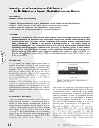
Figure 1: The circular piece of molybdenum placed in
the center of the sample.
After growth of the top foil layer, the sample was flipped over,
and a circular piece of molybdenum was placed in the center
of the sample (see Figure 1). A diamond layer for etch masking
was grown on the backside for two hours with conditions
similar to the topside foil layer. The molybdenum prevented
diamond from growing on part of the backside of the sample.
Some of the samples were annealed at 600°C for 20 hours in
a 5.0 sccm flow of N2
at a process pressure of 20 torr in an
attempt to reduce the internal stresses in the diamond foil.
The sample was placed in a 1:1:3 solution of 48% hydrofluoric,
70% nitric, and 100% acetic acids to etch a window in the
silicon. The ratio of acids determined the etch rate. If the etch
was too fast, the diamond came off in little pieces. If the etch
was too slow, it did not etch all the way through the silicon.
The backside layer of diamond protected the silicon outside
of the circle from the etch, yielding a suspended diamond foil
2. 79
M
A
T
S
•2014•NNIN•REU•Research•Accomplishments•
that was supported by the silicon. Once all of the silicon in the
circle was etched away, the sample was rinsed in DI water,
then allowed to air dry.
Results and Conclusions:
A high quality diamond foil was grown on a <100> piece
of silicon by HFCVD. Raman spectroscopy verified a high
quality diamond foil with a strong diamond peak at 1333 cm-1
and a very weak graphite peak as seen in Figure 2. Both SEM
and AFM showed the presence of polycrystalline diamond
as seen in Figure 3. A 1:1:3 acid ratio was found to be ideal
because it was not too fast or too slow. Using diamond as a
mask to protect the silicon during etching worked better than
wax by providing better mask control and greater resistance to
acid etching. AFM revealed that the foil originally against the
substrate had an average roughness of 6.7 nm, while the foil
away from the substrate had an average roughness of 13.2 nm.
SEM and optical imaging (see Figure 4) revealed no cracks in
the suspended foil. Both 6-hour diamond film growths did not
crack. The annealed sample appeared to be smoother, which
means that it had less internal stress. The 8-hour unannealed
diamond film growth cracked, while the 8-hour annealed film
growth did not. It appears that annealing the diamond foil
before etching away the silicon relieves some of the stresses
in the film.
Future Work:
Currently, the diamond foils that have been grown are under
much internal stress. Initial results suggested that pre-etching
annealing of the diamond is useful for relieving internal stress.
Future work should concentrate on various anneal temperature
and times for stress reduction. Another area of investigation
should involving introducing argon to the gas species during
diamond growth. Depending on the argon concentration
during growth, diamond grains can be reduced from poly to
nanocrystalline. Smaller grains may also reduce the stress in
the film. Lastly, foil testing by SNS should be performed to
verify diamond foil performance.
Acknowledgements:
I would like to thank the NNIN REU Program, the NSF, and
the Howard Nanoscale Facility (HNF). I would also like to
thank my PI, Dr. Gary Harris, and my mentor, Mr. James
Griffin, for their help and guidance, and Ms. Bokani Mtengi
for training me at Howard University. Lastly, I would like to
thank Dr. R.D. Vispute from Blue Wave Semiconductors for
his expertise on this project.
References:
[1] V.Kh. Liechtenstein, T.M. Ivkova, E.D. Olshanski, R. Repnow, J.
Levin, R. Hellborg, P. Persson, T. Schenkel. “Advances in targetry with
thin diamond-like carbon foils”; Nuclear Instruments and Methods in
Physics Research A, 480 (2002) 185-190.
[2] R.W. Shaw, D.P. Bontrager, L.L. Wilson, C.S. Feigerle, C.F. Luck,
M.A. Plum. “An Electron Beam SNS Foil Test Stand”; White Paper.
[3] T. Spickermann, M.J. Borden, R.J. Macek, R.W. Shaw, C.S. Feigerle,
I. Sugai. “Comparison of carbon and corrugated diamond stripper
foils under operational conditions at the Los Alamos PSR”; Nuclear
Instruments and Methods in Physics Research A, 590 (2008) 25-31.
[4] R.W. Shaw, V.A. Davis, R.N. Potter, L.L. Wilson, C.S. Feigerle, M.E.
Peretich, C.J. Liaw. “Corrugated Thin Diamond Foils for SNS H-
Injection Stripping”; White Paper.
[5] R.A. Campos, V.J. Trava-Airoldi, O.R. Bagnato, J.R. Moro, E.J. Corat.
“Development of nanocrystalline diamond windows for application in
synchrotron beamlines”; Vacuum 89 (2013) 21-25.
[6] RD Vispute, H.K. Ermer, P. Sinsky, A. Seiser, R.W. Shaw, G. Harris,
F. Piazza. “Nanodiamond Foil Product for H- Stripping to Support
Spallation Neutron Source (SNS) and Related Applications”; White
Paper.
Figure 4: Optical imaging reveals no cracks in
the suspended foil. (See full color version on
page xxxvi.)
Figure 2: Raman spectroscopy verifying a high
quality diamond foil with a strong diamond peak and
a very weak graphite peak.
Figure 3: SEM image verifying the
presence of polycrystalline diamond.
![79
M
A
T
S
•2014•NNIN•REU•Research•Accomplishments•
that was supported by the silicon. Once all of the silicon in the
circle was etched away, the sample was rinsed in DI water,
then allowed to air dry.
Results and Conclusions:
A high quality diamond foil was grown on a <100> piece
of silicon by HFCVD. Raman spectroscopy verified a high
quality diamond foil with a strong diamond peak at 1333 cm-1
and a very weak graphite peak as seen in Figure 2. Both SEM
and AFM showed the presence of polycrystalline diamond
as seen in Figure 3. A 1:1:3 acid ratio was found to be ideal
because it was not too fast or too slow. Using diamond as a
mask to protect the silicon during etching worked better than
wax by providing better mask control and greater resistance to
acid etching. AFM revealed that the foil originally against the
substrate had an average roughness of 6.7 nm, while the foil
away from the substrate had an average roughness of 13.2 nm.
SEM and optical imaging (see Figure 4) revealed no cracks in
the suspended foil. Both 6-hour diamond film growths did not
crack. The annealed sample appeared to be smoother, which
means that it had less internal stress. The 8-hour unannealed
diamond film growth cracked, while the 8-hour annealed film
growth did not. It appears that annealing the diamond foil
before etching away the silicon relieves some of the stresses
in the film.
Future Work:
Currently, the diamond foils that have been grown are under
much internal stress. Initial results suggested that pre-etching
annealing of the diamond is useful for relieving internal stress.
Future work should concentrate on various anneal temperature
and times for stress reduction. Another area of investigation
should involving introducing argon to the gas species during
diamond growth. Depending on the argon concentration
during growth, diamond grains can be reduced from poly to
nanocrystalline. Smaller grains may also reduce the stress in
the film. Lastly, foil testing by SNS should be performed to
verify diamond foil performance.
Acknowledgements:
I would like to thank the NNIN REU Program, the NSF, and
the Howard Nanoscale Facility (HNF). I would also like to
thank my PI, Dr. Gary Harris, and my mentor, Mr. James
Griffin, for their help and guidance, and Ms. Bokani Mtengi
for training me at Howard University. Lastly, I would like to
thank Dr. R.D. Vispute from Blue Wave Semiconductors for
his expertise on this project.
References:
[1] V.Kh. Liechtenstein, T.M. Ivkova, E.D. Olshanski, R. Repnow, J.
Levin, R. Hellborg, P. Persson, T. Schenkel. “Advances in targetry with
thin diamond-like carbon foils”; Nuclear Instruments and Methods in
Physics Research A, 480 (2002) 185-190.
[2] R.W. Shaw, D.P. Bontrager, L.L. Wilson, C.S. Feigerle, C.F. Luck,
M.A. Plum. “An Electron Beam SNS Foil Test Stand”; White Paper.
[3] T. Spickermann, M.J. Borden, R.J. Macek, R.W. Shaw, C.S. Feigerle,
I. Sugai. “Comparison of carbon and corrugated diamond stripper
foils under operational conditions at the Los Alamos PSR”; Nuclear
Instruments and Methods in Physics Research A, 590 (2008) 25-31.
[4] R.W. Shaw, V.A. Davis, R.N. Potter, L.L. Wilson, C.S. Feigerle, M.E.
Peretich, C.J. Liaw. “Corrugated Thin Diamond Foils for SNS H-
Injection Stripping”; White Paper.
[5] R.A. Campos, V.J. Trava-Airoldi, O.R. Bagnato, J.R. Moro, E.J. Corat.
“Development of nanocrystalline diamond windows for application in
synchrotron beamlines”; Vacuum 89 (2013) 21-25.
[6] RD Vispute, H.K. Ermer, P. Sinsky, A. Seiser, R.W. Shaw, G. Harris,
F. Piazza. “Nanodiamond Foil Product for H- Stripping to Support
Spallation Neutron Source (SNS) and Related Applications”; White
Paper.
Figure 4: Optical imaging reveals no cracks in
the suspended foil. (See full color version on
page xxxvi.)
Figure 2: Raman spectroscopy verifying a high
quality diamond foil with a strong diamond peak and
a very weak graphite peak.
Figure 3: SEM image verifying the
presence of polycrystalline diamond.](data:image/gif;base64,R0lGODlhAQABAIAAAAAAAP///yH5BAEAAAAALAAAAAABAAEAAAIBRAA7)