SlideShare a Scribd company logo
1 of 24
Digital communication systems
The communication that occurs in our day-to-
day life is in the form of signals. These signals,
such as sound signals, generally, are analog in
nature. When the communication needs to be
established over a distance, then the analog
signals are sent through wire, using different
techniques for effective transmission.
The Necessity of Digitization
The conventional methods of communication
used analog signals for long distance
communications, which suffer from many losses
such as distortion, interference, and other losses
including security breach.
In order to overcome these problems, the
signals are digitized using different techniques.
The digitized signals allow the communication to
be more clear and accurate without losses.
The following figure indicates the difference
between analog and digital signals. The digital
signals consist of 1s and 0s which indicate High
and Low values respectively.
Advantages of Digital
Communication
As the signals are digitized, there are many
advantages of digital communication over
analog communication, such as −
 The effect of distortion, noise, and
interference is much less in digital
signals as they are less affected.
 Digital circuits are more reliable.
 Digital circuits are easy to design and
cheaper than analog circuits.
 The hardware implementation in digital
circuits, is more flexible than analog.
 The occurrence of cross-talk is very rare
in digital communication.
 The signal is un-altered as the pulse
needs a high disturbance to alter its
properties, which is very difficult.
 Signal processing functions such as
encryption and compression are
employed in digital circuits to maintain the
secrecy of the information.
 The probability of error occurrence is
reduced by employing error detecting
and error correcting codes.
 Spread spectrum technique is used to
avoid signal jamming.
 Combining digital signals using Time
Division Multiplexing TDM is easier
than combining analog signals using
Frequency Division Multiplexing FDM.
 The configuring process of digital
signals is easier than analog signals.
 Digital signals can be saved and
retrieved more conveniently than
analog signals.
 Many of the digital circuits have almost
common encoding techniques and hence
similar devices can be used for a number
of purposes.
 The capacity of the channel is
effectively utilized by digital signals.
Elements of Digital
Communication
The elements which form a digital
communication system is represented by the
following block diagram for the ease of
understanding.
Following are the sections of the digital
communication system.
Source
The source can be an analog signal. Example:
A Sound signal
Input Transducer
This is a transducer which takes a physical input
and converts it to an electrical signal (Example:
microphone). This block also consists of
an analog to digital converter where a digital
signal is needed for further processes.
A digital signal is generally represented by a
binary sequence.
Source Encoder
The source encoder compresses the data into
minimum number of bits. This process helps in
effective utilization of the bandwidth.
It removes the redundant
bits unnecessary excess bits,i.e.,zeroes
Channel Encoder
The channel encoder, does the coding for error
correction. During the transmission of the signal,
due to the noise in the channel, the signal may
get altered and hence to avoid this, the channel
encoder adds some redundant bits to the
transmitted data. These are the error correcting
bits.
Digital Modulator
The signal to be transmitted is modulated here
by a carrier. The signal is also converted to
analog from the digital sequence, in order to
make it travel through the channel or medium.
Channel
The channel or a medium, allows the analog
signal to transmit from the transmitter end to the
receiver end.
Digital Demodulator
This is the first step at the receiver end. The
received signal is demodulated as well as
converted again from analog to digital. The
signal gets reconstructed here.
Channel Decoder
The channel decoder, after detecting the
sequence, does some error corrections. The
distortions which might occur during the
transmission, are corrected by adding some
redundant bits. This addition of bits helps in the
complete recovery of the original signal.
Source Decoder
The resultant signal is once again digitized by
sampling and quantizing so that the pure digital
output is obtained without the loss of
information. The source decoder recreates the
source output.
Output Transducer
This is the last block which converts the signal
into the original physical form, which was at the
input of the transmitter. It converts the electrical
signal into physical output (Example: loud
speaker).
Output Signal
This is the output which is produced after the
whole process. Example − The sound signal
received.
sampling
Sampling is defined as, “The process of
measuring the instantaneous values of
continuous-time signal in a discrete form.”
Sample is a piece of data taken from the whole
data which is continuous in the time domain.
When a source generates an analog signal and
if that has to be digitized, having 1s and 0s i.e.,
High or Low, the signal has to be discretized in
time. This discretization of analog signal is called
as Sampling.
The following figure indicates a continuous-time
signal x tt and a sampled signal xs tt.
When x tt is multiplied by a periodic impulse
train, the sampled signal xs tt is obtained.
Sampling Rate
To discretize the signals, the gap between the
samples should be fixed. That gap can be
termed as a sampling period Ts.
SamplingFrequency=1/Ts=fs
Where,
 Ts is the sampling time
 fs is the sampling frequency or the
sampling rate
Sampling frequency is the reciprocal of the
sampling period. This sampling frequency, can
be simply called as Sampling rate. The
sampling rate denotes the number of samples
taken per second, or for a finite set of values.
For an analog signal to be reconstructed from
the digitized signal, the sampling rate should be
highly considered. The rate of sampling should
be such that the data in the message signal
should neither be lost nor it should get over-
lapped. Hence, a rate was fixed for this, called
as Nyquist rate.
Nyquist Rate
Suppose that a signal is band-limited with no
frequency components higher than W Hertz.
That means, W is the highest frequency. For
such a signal, for effective reproduction of the
original signal, the sampling rate should be twice
the highest frequency.
Which means,
fS=2W
Where,
 fS is the sampling rate
 W is the highest frequency
This rate of sampling is called as Nyquist rate.
A theorem called, Sampling Theorem, was
stated on the theory of this Nyquist rate.
Sampling Theorem
The sampling theorem, which is also called
as Nyquist theorem, delivers the theory of
sufficient sample rate in terms of bandwidth for
the class of functions that are bandlimited.
The sampling theorem states that, “a signal can
be exactly reproduced if it is sampled at the
rate fs which is greater than twice the maximum
frequency W.”
To understand this sampling theorem, let us
consider a band-limited signal, i.e., a signal
whose value is non-zero between some –
W and W Hertz.
Such a signal is represented as
x(f)=0 for|f|>W
For the continuous-time signal x tt, the band-
limited signal in frequency domain, can be
represented as shown in the following figure.
We need a sampling frequency, a frequency at
which there should be no loss of information,
even after sampling. For this, we have the
Nyquist rate that the sampling frequency should
be two times the maximum frequency. It is the
critical rate of sampling.
If the signal xtt is sampled above the Nyquist
rate, the original signal can be recovered, and if
it is sampled below the Nyquist rate, the signal
cannot be recovered.
The following figure explains a signal, if sampled
at a higher rate than 2w in
the frequency domain.
The above figure shows the Fourier transform of
a signal xs(t). Here, the information is
reproduced without any loss. There is no mixing
up and hence recovery is possible.
The Fourier Transform of the signal xs(t) is
Xs(w)=1/Ts∑n=−∞ to ∞X(w−nw0)
Where Ts = Sampling Period and w0=2πTs
Let us see what happens if the sampling rate is
equal to twice the highest frequency (2W)
That means,
fs=2W
Where,
 fs is the sampling frequency
 W is the highest frequency
The result will be as shown in the above figure.
The information is replaced without any loss.
Hence, this is also a good sampling rate.
Now, let us look at the condition,
fs<2W
The resultant pattern will look like the following
figure.
We can observe from the above pattern that the
over-lapping of information is done, which leads
to mixing up and loss of information. This
unwanted phenomenon of over-lapping is called
as Aliasing.
Aliasing
Aliasing can be referred to as “the phenomenon
of a high-frequency component in the spectrum
of a signal, taking on the identity of a low-
frequency component in the spectrum of its
sampled version.”
The corrective measures taken to reduce the
effect of Aliasing are −
 In the transmitter section of PCM, a low
pass anti-aliasing filter is employed,
before the sampler, to eliminate the high
frequency components, which are
unwanted.
 The signal which is sampled after filtering,
is sampled at a rate slightly higher than
the Nyquist rate.
This choice of having the sampling rate higher than
Nyquist rate,also helps in the easier design of
the reconstruction filter at the receiver.
Scope of Fourier Transform
It is generally observed that, we seek the help of
Fourier series and Fourier transforms in
analyzing the signals and also in proving
theorems. It is because −
 The Fourier Transform is the extension of
Fourier series for non-periodic signals.
 Fourier transform is a powerful
mathematical tool which helps to view the
signals in different domains and helps to
analyze the signals easily.
 Any signal can be decomposed in terms
of sum of sines and cosines using this
Fourier transform.
The digitization of analog signals involves the
rounding off of the values which are
approximately equal to the analog values. The
method of sampling chooses a few points on the
analog signal and then these points are joined to
round off the value to a near stabilized value.
Such a process is called as Quantization.
Quantizing an Analog Signal
The analog-to-digital converters perform this
type of function to create a series of digital
values out of the given analog signal. The
following figure represents an analog signal.
This signal to get converted into digital, has to
undergo sampling and quantizing.
The quantizing of an analog signal is done by
discretizing the signal with a number of
quantization levels. Quantization is
representing the sampled values of the
amplitude by a finite set of levels, which means
converting a continuous-amplitude sample into a
discrete-time signal.
The following figure shows how an analog signal
gets quantized. The blue line represents analog
signal while the brown one represents the
quantized signal.
Both sampling and quantization result in the loss
of information. The quality of a Quantizer output
depends upon the number of quantization levels
used. The discrete amplitudes of the quantized
output are called as representation
levels or reconstruction levels. The spacing
between the two adjacent representation levels
is called a quantum or step-size.
The following figure shows the resultant
quantized signal which is the digital form for the
given analog signal.
This is also called as Stair-case waveform, in
accordance with its shape.
Types of Quantization
There are two types of Quantization - Uniform
Quantization and Non-uniform Quantization.
The type of quantization in which the
quantization levels are uniformly spaced is
termed as a Uniform Quantization. The type of
quantization in which the quantization levels are
unequal and mostly the relation between them is
logarithmic, is termed as a Non-uniform
Quantization.
There are two types of uniform quantization.
They are Mid-Rise type and Mid-Tread type. The
following figures represent the two types of
uniform quantization.
Figure 1 shows the mid-rise type and figure 2
shows the mid-tread type of uniform
quantization.
 The Mid-Rise type is so called because
the origin lies in the middle of a raising
part of the stair-case like graph. The
quantization levels in this type are even
in number.
 The Mid-tread type is so called because
the origin lies in the middle of a tread
of the stair-case like graph. The
quantization levels in this type are odd in
number.
 Both the mid-rise and mid-tread type of
uniform quantizers are symmetric about
the origin.
Quantization Error
For any system, during its functioning, there is
always a difference in the values of its input and
output. The processing of the system results in
an error, which is the difference of those values.
The difference between an input value and its
quantized value is called a Quantization Error.
A Quantizer is a logarithmic function that
perform Quantization rounding off the value.
An analog-to-digital converter (ADC) works as a
quantizer.
The following figure illustrates an example for a
quantization error, indicating the difference
between the original signal and the quantized
signal.
Quantization Noise
It is a type of quantization error, which usually
occurs in analog audio signal, while quantizing it
to digital. For example, in music, the signals
keep changing continuously, where a regularity
is not found in errors. Such errors create a
wideband noise called as Quantization Noise.
Advantages of Non – Uniform Quantization :
1. Higher average signal to quantization
noise power ratio than the uniform quantizer
when the signal pdf is non uniform which is the
case in many practical situation.
2. RMS value of the quantizer noise power of a
non – uniform quantizer is substantially
proportional to the sampled value and hence
the effect of the quantizer noise is reduced.
Companding in PCM
The word Companding is a combination of
Compressing and Expanding, which means that
it does both. This is a non-linear technique used
in PCM which compresses the data at the
transmitter and expands the same data at the
receiver. The effects of noise and crosstalk are
reduced by using this technique.
 Companding is the process of compression
and then expansion. With companded
system, the higher amplitude analog
signals are compressed (amplified less
than lower amplitude signals) prior to
transmission and then expanded
(amplified more than the lower amplitude
signals) in the receiver.
Fig. 1 Block diagram of Companded PCM
system
 Companding is used in pulse code
modulation (PCM). The process involves
decreasing the number of bits used to
record the strongest (loudest) signals.
 In the digital file format, companding
improves the signal-to-noise ratio at
reduced bit rates. For example, a 16-bit
PCM signal may be converted to an eight-
bit ".wav" or ".au" file.
 µ-law companding is used for speech and
music signals.
 µ-law is used in North America and Japan.
 The process of compression of the signal at
the transmitter and expansion at the
receiver is called as companding
(compression and expansion).
 In companding, the higheramplitude
analogsignals are compressed preceding
transmission and then expanded in the
receiver.
 Companding is performed with the help of
three functional blocks, which are
Compressor, Uniform quantizerand
Expander and the diagram in shown below
in the Fig1.
Fig1. Compander Functional Blocks
 The compressor will compressthe dynamic
rangeof the signal so that high dynamic
range signal can be passed through
components of low dynamic range
capability, the uniform quantizer will
undergo the quantization process of the
compressed signal and the lastly the
expanderwill undergo expansion andinvert
the compressionfunction to reconstruct the
original signal.
 The expander has complementary
characteristics as that of compressor so
that the compressor input is equal to
expanderoutput in order to reproduce the
signal at the receiver.
 The Fig2 below illustrates the input-output
characteristics and curves of the
companding process, and it can be seen
that companding has linearcharacteristics.
 It helps in minimizing noise, distortion,
interference and reduction in the levels of
crosstalk.
 Companding helps in improving the
dynamic range of the communication
systems.
 Companding is used in telephony and other
audio applications.
1. In companding, we convert the signal into
digital domain non-linearly to achieve
compression.
2. Here the weakersignals areamplifiedby
largerfactors while the stronger signals are
amplified by smallerfactors.
3. There are two types of companding:
o μ-law companding
o A-law companding
A-law Companding Technique
 Uniform quantization is achieved at A = 1,
where the characteristic curve is linear
and no compression is done.
 A-law has mid-rise at the origin. Hence, it
contains a non-zero value.
 A-law companding is used for PCM
telephone systems.
µ-law Companding Technique
 Uniform quantization is achieved at µ = 0,
where the characteristic curve is linear
and no compression is done.
 µ-law has mid-tread at the origin. Hence,
it contains a zero value.
4. The μ-law and A-law companding
standards employ logarithm based
functions to encodeaudio samples forISDN
(Integrated Services Digital Network)
digital telephony services by means of non-
linear quantization.
μ-law companding
 It is used in North America and Japan.
 It uses the fact that low amplitude of
speech signal contain more information
than high amplitude.
 Hence we can use non-linear quantization.
 μ-law encoder inputs 14bit samples and
outputs 8 bit codewords.
 Since encoder receives 14 bit signed input
sample x, the input range is (-8192,
+8191).
 This input sample is normalised to the
interval (-1, +1) using the following
logarithmic expression:
8 bit code = sgn(x)(ln [1+μ|x|])/(ln [1+|μ|])
|x|<=1
Where sgn(x) = where μ=0 to 255.
 The 8-bit codeword in (-1, 1) is then scaled
to the range (-256, 255) using following
format recommended by G.711 standard.
Here, P represents the sign of the input sample.
Bits S2, S1 and S0 are the segment code. Q3, Q2
and Q0 are the quantization code.
Encoder:
 The encoder determines the segment code
by adding a bias of 33 to the absolute value
of input sample.
 Determining the bit position of the most
significant one bit among bits 5 to 12 of the
input and subtracting 5 from that position.
 The 4 bit quantization code is set to 4 bits
following the bit position determined in
step b.
 The encoder ignores the remaining bits of
the input sample and inverts the code word
at its output.
Decoder:
 The quantization code is multiplied by 2
and then the bias of 33 is added to the
result.
 The result of step a. is multiplied by 2SC
where SC is segment code.
 This result is decremented by a bias of 33.
 The sign of the result is determined using
bit P.
A-law companding
 The A-law compander has a midriser and is
defined by

Encoder:
 The A-law encoder inputs 13 bit samples
and outputs 8 bit code words.
 The range of signed input is (-4096,
+4095) and this input sample x is
normalised to interval (-1, 1) using
logarithmic expression.
8 bit code = sgn(x) (A|x|)/(1+ln(A)) for0 ≤
|x|≤1/A
=sgn(x) (1+ln(A|x|))/(1+ln(A)) for1/A ≤ |x|
≤ 1
This code word is then scaled to (-256, 255) using
following format recommended by G.711
standard.
P S1 S2 S0 Q3 Q2 Q1 Q0
The bit pattern P determines the sign of the input
samples.
The segment code is determined as
A) Determine the bit position of the most
significant bit in the input.
B) If such a position is found, the segment code
becomes the position determined in step a. minus
4 otherwise it becomes 0.
C) The 4 bit QC is set to the 4 bits following the bit
position determined in step a. or half of the input
value if the segment code is 0.
D) The encoder ignores the remaining bits of the
input sample and it inverts the bit P and the even
numbered bits of the code word bit it is output.
Decoder:
A) It inverts bit P and the even numbered bits of
the code.
B) If the segment code is non-zero, the decoder
multiplies the quantization code by 2 and
increments this by a bias of 33. This result is then
multiplied by 2SC – 1.
C) Bit P is used to determine the sign of the output
sample.
Pulse Code Modulation
Modulation is the process of varying one or
more parameters of a carrier signal in
accordance with the instantaneous values of the
message signal.
The message signal is the signal which is being
transmitted for communication and the carrier
signal is a high frequency signal which has no
data, but is used for long distance transmission.
There are many modulation techniques, which
are classified according to the type of
modulation employed. Of them all, the digital
modulation technique used is Pulse Code
Modulation PCM.
A signal is pulse code modulated to convert its
analog information into a binary sequence,
i.e., 1s and 0s. The output of a PCM will
resemble a binary sequence. The following
figure shows an example of PCM output with
respect to instantaneous values of a given sine
wave.
Instead of a pulse train, PCM produces a series
of numbers or digits, and hence this process is
called as digital. Each one of these digits,
though in binary code, represent the
approximate amplitude of the signal sample at
that instant.
In Pulse Code Modulation, the message signal
is represented by a sequence of coded pulses.
This message signal is achieved by representing
the signal in discrete form in both time and
amplitude.
Basic Elements of PCM
The transmitter section of a Pulse Code
Modulator circuit consists of Sampling,
Quantizing and Encoding, which are
performed in the analog-to-digital converter
section. The low pass filter prior to sampling
prevents aliasing of the message signal.
The basic operations in the receiver section
are regeneration of impaired signals,
decoding, and reconstruction of the
quantized pulse train. Following is the block
diagram of PCM which represents the basic
elements of both the transmitter and the receiver
sections.
Low Pass Filter
This filter eliminates the high frequency
components present in the input analog signal
which is greater than the highest frequency of
the message signal, to avoid aliasing of the
message signal.
Sampler
This is the technique which helps to collect the
sample data at instantaneous values of
message signal, so as to reconstruct the original
signal. The sampling rate must be greater than
twice the highest frequency component W of the
message signal, in accordance with the
sampling theorem.
Quantizer
Quantizing is a process of reducing the
excessive bits and confining the data. The
sampled output when given to Quantizer,
reduces the redundant bits and compresses the
value.
Encoder
The digitization of analog signal is done by the
encoder. It designates each quantized level by a
binary code. The sampling done here is the
sample-and-hold process. These three
sections LPF,Sampler,andQuantizer will act as an
analog to digital converter. Encoding minimizes
the bandwidth used.
Regenerative Repeater
This section increases the signal strength.
The output of the channel also has one
regenerative repeater circuit, to compensate the
signal loss and reconstruct the signal, and also
to increase its strength.
Decoder
The decoder circuit decodes the pulse coded
waveform to reproduce the original signal. This
circuit acts as the demodulator.
Reconstruction Filter
After the digital-to-analog conversion is done by
the regenerative circuit and the decoder, a low-
pass filter is employed, called as the
reconstruction filter to get back the original
signal.
Hence, the Pulse Code Modulator circuit
digitizes the given analog signal, codes it and
samples it, and then transmits it in an analog
form. This whole process is repeated in a
reverse pattern to obtain the original signal.
LINE CODING IN DIGITAL COMMUNICATION
>> WHAT IS LINE CODING?
In telecommunication, a line code (also called
digital baseband modulation, also called
digital baseband transmission method) is a
code chosen for use within a communications
system for baseband transmission purposes.
Line coding is often used for digital data
transport.
Binary 1’s and 0’s, such as in PCM signaling,
may be represented in various serial–bit
signaling formats called line codes.
WHY LINE CODING?
There are many reasons for using line coding.
Each of the line codes you will be examining
offers one or more of the following advantages:
 Spectrum Shaping and Relocation without
modulation or filtering. This is important in
telephone line applications, for example,
where the transfer characteristic has heavy
attenuation below 300 Hz.
 Bit clock recovery can be simplified.
 DC component can be eliminated; this
allows AC (capacitor or transformer) coupling
between stages (as in telephone lines). Can
control baseline wander (baseline wander
shifts the position of the signal waveform
relative to the detector threshold and leads to
severe erosion of noise margin).
 Error detection capabilities.
 Bandwidth usage; the possibility of
transmitting at a higher rate than other
schemes over the same bandwidth.
At the very least the LINE-CODE ENCODER
serves as an interface between the TTL level
signals of the transmitter and those of the
analog channel. Likewise, the LINE-CODE
DECODER serves as an interface between the
analog signals of the channel and the TTL level
signals required by the digital receiver.
>> MOST POPULAR LINE CODES
Some of the most popular line codes are shown
below.The line codes shown above are also
known by other names:
Polar NRZ: Also called NRZ–L where L denotes
the normal logic level assignment
Bipolar RZ: Also called RZ–AMI, where AMI
denotes alternate mark (binary 1) inversion
Bipolar NRZ: Also called NRZ–M, where M
denotes inversion on mark (binary 1)
A line code is the code used for data
transmission of a digital signal over a
transmission line. This process of coding is
chosen so as to avoid overlap and distortion of
signal such as inter-symbol interference.
Properties of Line Coding
Following are the properties of line coding −
 As the coding is done to make more bits
transmit on a single signal, the
bandwidth used is much reduced.
 For a given bandwidth, the power is
efficiently used.
 The probability of error is much
reduced.
 Error detection is done and the bipolar
too has a correction capability.
 Power density is much favorable.
 The timing content is adequate.
 Long strings of 1s and 0s is avoided to
maintain transparency.
Types of Line Coding
There are 3 types of Line Coding
 Unipolar
 Polar
 Bi-polar
Unipolar Signaling
Unipolar signaling is also called as On-Off
Keying or simply OOK.
The presence of pulse represents a 1 and the
absence of pulse represents a 0.
There are two variations in Unipolar signaling −
 Non Return to Zero NRZ
 Return to Zero RZ
Unipolar Non-Return to Zero NRZ
In this type of unipolar signaling, a High in data
is represented by a positive pulse called
as Mark, which has a duration T0 equal to the
symbol bit duration. A Low in data input has no
pulse.
The following figure clearly depicts this.
Advantages
The advantages of Unipolar NRZ are −
 It is simple.
 A lesser bandwidth is required.
Disadvantages
The disadvantages of Unipolar NRZ are −
 No error correction done.
 Presence of low frequency components
may cause the signal droop.
 No clock is present.
 Loss of synchronization is likely to
occur (especially for long strings
of 1s and 0s).
Unipolar Return to Zero RZ
In this type of unipolar signaling, a High in data,
though represented by a Mark pulse, its
duration T0 is less than the symbol bit duration.
Half of the bit duration remains high but it
immediately returns to zero and shows the
absence of pulse during the remaining half of the
bit duration.
It is clearly understood with the help of the
following figure.
Advantages
The advantages of Unipolar RZ are −
 It is simple.
 The spectral line present at the symbol rate
can be used as a clock.
Disadvantages
The disadvantages of Unipolar RZ are −
 No error correction.
 Occupies twice the bandwidth as unipolar
NRZ.
 The signal droop is caused at the places
where signal is non-zero at 0 Hz.
Polar Signaling
There are two methods of Polar Signaling. They
are −
 Polar NRZ
 Polar RZ
Polar NRZ
In this type of Polar signaling, a High in data is
represented by a positive pulse, while a Low in
data is represented by a negative pulse. The
following figure depicts this well.
Advantages
The advantages of Polar NRZ are −
 It is simple.
 No low-frequency components are present.
Disadvantages
The disadvantages of Polar NRZ are −
 No error correction.
 No clock is present.
 The signal droop is caused at the places
where the signal is non-zero at 0 Hz.
Polar RZ
In this type of Polar signaling, a High in data,
though represented by a Mark pulse, its
duration T0 is less than the symbol bit duration.
Half of the bit duration remains high but it
immediately returns to zero and shows the
absence of pulse during the remaining half of the
bit duration.
However, for a Low input, a negative pulse
represents the data, and the zero level remains
same for the other half of the bit duration. The
following figure depicts this clearly.
Advantages
The advantages of Polar RZ are −
 It is simple.
 No low-frequency components are present.
Disadvantages
The disadvantages of Polar RZ are −
 No error correction.
 No clock is present.
 Occupies twice the bandwidth of Polar
NRZ.
 The signal droop is caused at places
where the signal is non-zero at 0 Hz.
Bipolar Signaling
This is an encoding technique which has three
voltage levels namely +, - and 0. Such a signal
is called as duo-binary signal.
An example of this type is Alternate Mark
Inversion AMI. For a 1, the voltage level gets a
transition from + to – or from – to +, having
alternate 1s to be of equal polarity. A 0 will have
a zero voltage level.
Even in this method, we have two types.
 Bipolar NRZ
 Bipolar RZ
From the models so far discussed, we have
learnt the difference between NRZ and RZ. It
just goes in the same way here too. The
following figure clearly depicts this.
The above figure has both the Bipolar NRZ and
RZ waveforms. The pulse duration and symbol
bit duration are equal in NRZ type, while the
pulse duration is half of the symbol bit duration
in RZ type.
Advantages
Following are the advantages −
 It is simple.
 No low-frequency components are
present.
 Occupies low bandwidth than unipolar
and polar NRZ schemes.
 This technique is suitable for
transmission over AC coupled lines,
as signal drooping doesn’t occur here.
 A single error detection capability is
present in this.
Disadvantages
Following are the disadvantages −
 No clock is present.
 Long strings of data causes loss of
synchronization.
>> DIFFERENTIAL CODING
When serial data is passed through many
circuits along a communication channel, the
waveform is often unintentionally inverted (i.e.
data complemented). This result can occur in a
twisted pair transmission line channel just by
switching the 2 leads at a connection point when
a polar line code is used. (Note: such switching
would not affect the data of a bipolar signal)
To eliminate this problem differential encoding is
often employed.
Each digit in an differential encoded sequence is
obtained by comparing the present input bit with
the past encoded bit. A binary 1 is encoded if
the present input bit and past encoded bit are of
opposite state. A binary 0 is encoded if the
states are the same.
Differential coding is often used with Manchester
coding.
Differential pulse code modulation
For the samples that are highly correlated, when
encoded by PCM technique, leave redundant
information behind. To process this redundant
information and to have a better output, it is a
wise decisionto take a predicted sampled value,
assumed from its previous output and
summarize them with the quantized values.
Such a process is called as Differential
PCM DPCMtechnique.
DPCM Transmitter
The DPCM Transmitter consists of Quantizer
and Predictor with two summer circuits.
Following is the block diagram of DPCM
transmitter.
The signals at each point are named as −
 x(nTs) is the sampled input
 xˆ(nTs) is the predicted sample
 e(nTs) is the difference of sampled input
and predicted output, often called as
prediction error
 v(nTs)is the quantized output
 u(nTs)is the predictor input which is
actually the summer output of the
predictor output and the quantizer output
The predictor produces the assumed samples
from the previous outputs of the transmitter
circuit. The input to this predictor is the
quantized versions of the input signal x(nTs).
Quantizer Output is represented as −
v(nTs)=Q[e(nTs)]
=e(nTs)+q(nTs)
=e(nTs)+q(nTs)
Where q (nTs) is the quantization error
Predictor input is the sum of quantizer output
and predictor output,
u(nTs)=xˆ(nTs)+v(nTs)
u(nTs)=xˆ(nTs)+e(nTs)+q(nTs)
u(nTs)=x(nTs)+q(nTs)
The same predictor circuit is used in the decoder
to reconstruct the original input.
DPCM Receiver
The block diagram of DPCM Receiver consists
of a decoder, a predictor, and a summer circuit.
Following is the diagram of DPCM Receiver.
The notation of the signals is the same as the
previous ones. In the absence of noise, the
encoded receiver input will be the same as the
encoded transmitter output.
As mentioned before, the predictor assumes a
value, based on the previous outputs. The input
given to the decoder is processed and that
output is summed up with the output of the
predictor, to obtain a better output.
Prediction gain:
Adaptive differential pulse code modulation:
Time division multiplexing
TDM is the time interleaving of samples from
several sources so that the information from
these sources can be transmitted serially over a
single communication channel.
At the receiver the decommutator (sampler) has
to be synchronized with the incoming waveform
so that the PAM samples corresponding to
source-1 will appear on the channel-1 output.
Synchronisation
Frame synchronization is needed at the TDM
receiver so that the received multiplexed data
can be sorted and directed to appropriate output
channel.
Frame sync is provided to the receiver in two
different ways:
>> provided to the de-multiplexer circuit by
sending a frame sync signal from the transmitter
over a separate channel
>> derive the frame sync from the TDM signal
itself
Figure show that frame sync can be multiplexed
along with the information words in an N channel
TDM system.
Figure shows that the frame sync is recovered
from the corrupted TDM signal by using a frame
synchronizer circuit which crosscorrelates the
regenerated TDM signal with the expected
unique sync word vector s = (s1,s2,…,sK).
Multiplexing
Multiplexing is the process of combining
multiple signals into one signal, over a shared
medium. These signals, if analog in nature, the
process is called as analog multiplexing. If
digital signals are multiplexed, it is called
as digital multiplexing.
Multiplexing was first developed in telephony. A
number of signals were combined to send
through a single cable. The process of
multiplexing divides a communication channel
into several number of logical channels, allotting
each one for a different message signal or a data
stream to be transferred. The device that does
multiplexing, can be called as a MUX. The
reverse process, i.e., extracting the number of
channels from one, which is done at the receiver
is called as de-multiplexing. The device which
does de-multiplexing is called as DEMUX.
The following figures represent MUX and
DEMUX. Their primary use is in the field of
communications.
Types of Multiplexers
There are mainly two types of multiplexers,
namely analog and digital. They are further
divided into FDM, WDM, and TDM. The
following figure gives a detailed idea on this
classification.
Actually, there are many types of multiplexing
techniques. Of them all, we have the main types
with general classification, mentioned in the
above figure.
Analog Multiplexing
The analog multiplexing techniques involve
signals which are analog in nature. The analog
signals are multiplexed according to their
frequency FDM or wavelength WDM.
Frequency Division Multiplexing FDMFDM
In analog multiplexing, the most used technique
is Frequency Division Multiplexing FDM. This
technique uses various frequencies to combine
streams of data, for sending them on a
communication medium, as a single signal.
Example − A traditional television transmitter,
which sends a number of channels through a
single cable, uses FDM.
Wavelength Division Multiplexing WDM
Wavelength Division multiplexing is an analog
technique, in which many data streams of
different wavelengths are transmitted in the light
spectrum. If the wavelength increases, the
frequency of the signal decreases.
A prism which can turn different wavelengths
into a single line, can be used at the output of
MUX and input of DEMUX.
Example − Optical fiber communications use
WDM technique to merge different wavelengths
into a single light for communication.
Digital Multiplexing
The term digital represents the discrete bits of
information. Hence, the available data is in the
form of frames or packets, which are discrete.
Time Division Multiplexing TDM
In TDM, the time frame is divided into slots. This
technique is used to transmit a signal over a
single communication channel, by allotting one
slot for each message.
Of all the types of TDM, the main ones are
Synchronous and Asynchronous TDM.
Synchronous TDM
In Synchronous TDM, the input is connected to
a frame. If there are ‘n’ number of connections,
then the frame is divided into ‘n’ time slots. One
slot is allocated for each input line.
In this technique, the sampling rate is common
to all signals and hence the same clock input is
given. The MUX allocates the same slot to each
device at all times.
Asynchronous TDM
In Asynchronous TDM, the sampling rate is
different for each of the signals and a common
clock is not required. If the allotted device, for a
time-slot, transmits nothing and sits idle, then
that slot is allotted to another device, unlike
synchronous. This type of TDM is used in
Asynchronous transfer mode networks.
Regenerative Repeater
For any communication system to be reliable, it
should transmit and receive the signals
effectively, without any loss. A PCM wave, after
transmitting through a channel, gets distorted
due to the noise introduced by the channel.
The regenerative pulse compared with the
original and received pulse, will be as shown in
the following figure.
For a better reproduction of the signal, a circuit
called as regenerative repeater is employed in
the path before the receiver. This helps in
restoring the signals from the losses occurred.
Following is the diagrammatical representation.
This consists of an equalizer along with an
amplifier, a timing circuit, and a decision making
device. Their working of each of the components
is detailed as follows.
Equalizer
The channel produces amplitude and phase
distortions to the signals. This is due to the
transmission characteristics of the channel. The
Equalizer circuit compensates these losses by
shaping the received pulses.
Timing Circuit
To obtain a quality output, the sampling of the
pulses should be done where the signal to noise
ratio SNR is maximum. To achieve this perfect
sampling, a periodic pulse train has to be
derived from the received pulses, which is done
by the timing circuit.
Hence, the timing circuit, allots the timing
interval for sampling at high SNR, through the
received pulses.
Decision Device
The timing circuit determines the sampling
times. The decision device is enabled at these
sampling times. The decision device decides its
output based on whether the amplitude of the
quantized pulse and the noise, exceeds a pre-
determined value or not.
These are few of the techniques used in digital
communications. There are other important
techniques to be learned, called as data
encoding techniques. Let us learn about them in
the subsequent chapters, after taking a look at
the line codes.
Intro to delta modulation:
The sampling rate of a signal should be higher
than the Nyquist rate, to achieve better
sampling. If this sampling interval in Differential
PCM is reduced considerably, the sampleto-
sample amplitude difference is very small, as if
the difference is 1-bit quantization, then the
step-size will be very small i.e., Δ deltadelta.
Delta Modulation
The type of modulation, where the sampling rate
is much higher and in which the stepsize after
quantization is of a smaller value Δ, such a
modulation is termed as delta modulation.
Features of Delta Modulation
Following are some of the features of delta
modulation.
 An over-sampled input is taken to make
full use of the signal correlation.
 The quantization design is simple.
 The input sequence is much higher than
the Nyquist rate.
 The quality is moderate.
 The design of the modulator and the
demodulator is simple.
 The stair-case approximation of output
waveform.
 The step-size is very small, i.e., Δ delta.
 The bit rate can be decided by the user.
 This involves simpler implementation.
Delta Modulation is a simplified form of DPCM
technique, also viewed as 1-bit DPCM scheme.
As the sampling interval is reduced, the signal
correlation will be higher.
Delta Modulator
The Delta Modulator comprises of a 1-bit
quantizer and a delay circuit along with two
summer circuits. Following is the block diagram
of a delta modulator.
The predictor circuit in DPCM is replaced by a
simple delay circuit in DM.
From the above diagram, we have the notations
as −
 x(nTs) = over sampled input
 ep(nTs) = summer output and quantizer
input
 eq(nTs)=quantizeroutput= v(nTs)
 x^(nTs) = output of delay circuit
 u(nTs) = input of delay circuit
Using these notations, now we shall try to figure
out the process of delta modulation.
ep(nTs)=x(nTs)−xˆ(nTs) ----eqn 1
=x(nTs)−u([n−1]Ts)
=x(nTs)−[xˆ[[n−1]Ts]+v[[n−1]Ts]]----eqn 2
Further,
v(nTs)=eq(nTs)=S.sig.[ep(nTs)]----eqn 3
u(nTs)=xˆ(nTs)+eq(nTs)
Where,
 xˆ(nTs) = the previous value of the delay
circuit
 eq(nTs)=quantizeroutput= v(nTs)
Hence,u(nTs)=u([n−1]Ts)+v(nTs)----eqn 4
Which means,
The present input of the delay unit
= Thepreviousoutputofthedelayunit + thepresen
tquantizeroutput
Assuming zero condition of Accumulation,
u(nTs)=S∑j=1tonsig[ep(jTs)]
Accumulated version of DM
output = ∑j=1tonv(jTs)----eqn 5
Now, note that
xˆ(nTs)=u([n−1]Ts)
xˆ(nTs)=∑j=1ton−1v(jTs)--eqn 6
Delay unit output is an Accumulator output
lagging by one sample.
From equations 5 & 6, we get a possible
structure for the demodulator.
A Stair-case approximated waveform will be the
output of the delta modulator with the step-size
as delta (Δ). The output quality of the waveform
is moderate.
Delta Demodulator
The delta demodulator comprises of a low pass
filter, a summer, and a delay circuit. The
predictor circuit is eliminated here and hence no
assumed input is given to the demodulator.
Following is the diagram for delta demodulator.
From the above diagram, we have the notations
as −
 vˆ(nTs) is the input sample
 uˆ(nTs) is the summer output
 x¯(nTs) is the delayed output
A binary sequence will be given as an input to
the demodulator. The stair-case approximated
output is given to the LPF.
Low pass filter is used for many reasons, but the
prominent reason is noise elimination for out-of-
band signals. The step-size error that may occur
at the transmitter is called granular noise,
which is eliminated here. If there is no noise
present, then the modulator output equals the
demodulator input.
Advantages of DM Over DPCM
 1-bit quantizer
 Very easy designof the modulator and the
demodulator
However, there exists some noise in DM.
 Slope Over load distortion (when Δ is
small)
 Granular noise (when Δ is large)
Adaptive Delta Modulation ADM
In digital modulation, we have come across
certain problem of determining the step-size,
which influences the quality of the output wave.
A larger step-size is needed in the steep slope
of modulating signal and a smaller stepsize is
needed where the message has a small slope.
The minute details get missed in the process.
So, it would be better if we can control the
adjustment of step-size, according to our
requirement in order to obtain the sampling in a
desired fashion. This is the concept of Adaptive
Delta Modulation.
Following is the block diagram of Adaptive delta
modulator.
The gain of the voltage controlled amplifier is
adjusted by the output signal from the sampler.
The amplifier gain determines the step-size and
both are proportional.
ADM quantizes the difference between the
value of the current sample and the predicted
value of the next sample. It uses a variable
step height to predict the next values, for the
faithful reproduction of the fast varying values.
Source coding systems

More Related Content

What's hot

What's hot (20)

Digital signal processing
Digital signal processingDigital signal processing
Digital signal processing
 
Pluse amplitude modulatiion
Pluse amplitude modulatiionPluse amplitude modulatiion
Pluse amplitude modulatiion
 
Sonet (synchronous optical networking )
Sonet (synchronous optical networking )Sonet (synchronous optical networking )
Sonet (synchronous optical networking )
 
Pulse Code Modulation
Pulse Code ModulationPulse Code Modulation
Pulse Code Modulation
 
Source coding
Source coding Source coding
Source coding
 
Pulse code modulation
Pulse code modulationPulse code modulation
Pulse code modulation
 
Frequency-Shift Keying
Frequency-Shift KeyingFrequency-Shift Keying
Frequency-Shift Keying
 
Digital base band modulation
Digital base band modulationDigital base band modulation
Digital base band modulation
 
Delta Modulation
Delta ModulationDelta Modulation
Delta Modulation
 
4.Sampling and Hilbert Transform
4.Sampling and Hilbert Transform4.Sampling and Hilbert Transform
4.Sampling and Hilbert Transform
 
Pulse amplitude modulation
Pulse amplitude modulationPulse amplitude modulation
Pulse amplitude modulation
 
Frequency modulation
Frequency modulationFrequency modulation
Frequency modulation
 
8 modulación, am, fm, pm, etc.
8   modulación, am, fm, pm, etc.8   modulación, am, fm, pm, etc.
8 modulación, am, fm, pm, etc.
 
Eye diagram in Communication
Eye diagram in CommunicationEye diagram in Communication
Eye diagram in Communication
 
ASk,FSK,PSK
ASk,FSK,PSKASk,FSK,PSK
ASk,FSK,PSK
 
Actividad no.2 grupal
Actividad no.2 grupalActividad no.2 grupal
Actividad no.2 grupal
 
4.5 equalizers and its types
4.5   equalizers and its types4.5   equalizers and its types
4.5 equalizers and its types
 
Pulse modulation
Pulse modulationPulse modulation
Pulse modulation
 
Introduction to dsp
Introduction to dspIntroduction to dsp
Introduction to dsp
 
Modulacion-digital
 Modulacion-digital Modulacion-digital
Modulacion-digital
 

Similar to Source coding systems

BEC604 -COMMUNICATION ENG II.pdf
BEC604 -COMMUNICATION ENG II.pdfBEC604 -COMMUNICATION ENG II.pdf
BEC604 -COMMUNICATION ENG II.pdfSunil Manjani
 
PCM and delta modulation.ppt
PCM and delta modulation.pptPCM and delta modulation.ppt
PCM and delta modulation.ppt1637ARUNIMADAS
 
TeleCom Lecture 07.ppt
TeleCom Lecture 07.pptTeleCom Lecture 07.ppt
TeleCom Lecture 07.pptRiyaBatool
 
analog communication system for undergraduate .pdf
analog communication  system for undergraduate .pdfanalog communication  system for undergraduate .pdf
analog communication system for undergraduate .pdfAlaAwouda
 
Introduction to communication system lecture4
Introduction to communication system lecture4Introduction to communication system lecture4
Introduction to communication system lecture4Jumaan Ally Mohamed
 
Ch4 1 Data communication and networking by neha g. kurale
Ch4 1 Data communication and networking by neha g. kuraleCh4 1 Data communication and networking by neha g. kurale
Ch4 1 Data communication and networking by neha g. kuraleNeha Kurale
 
COMPUTER NETWORKS DATAS AND SIGNALS.pptx
COMPUTER NETWORKS DATAS AND SIGNALS.pptxCOMPUTER NETWORKS DATAS AND SIGNALS.pptx
COMPUTER NETWORKS DATAS AND SIGNALS.pptxKALPANAC20
 
Analog to digital conversion technique
Analog to digital conversion techniqueAnalog to digital conversion technique
Analog to digital conversion techniqueUmar Shuaib
 
Unit 4 Pulse Modulation.pdf
Unit 4 Pulse Modulation.pdfUnit 4 Pulse Modulation.pdf
Unit 4 Pulse Modulation.pdfTejasAuti4
 
Sensor technology module-3-interface electronic circuits
Sensor technology module-3-interface electronic circuitsSensor technology module-3-interface electronic circuits
Sensor technology module-3-interface electronic circuitsSweta Kumari Barnwal
 
24071 digitalcommunication
24071 digitalcommunication24071 digitalcommunication
24071 digitalcommunicationsharma ellappan
 
4. Analog to digital conversation (1).ppt
4. Analog to digital conversation (1).ppt4. Analog to digital conversation (1).ppt
4. Analog to digital conversation (1).ppttest22333
 
Telecommunications basics
Telecommunications basicsTelecommunications basics
Telecommunications basicsAarón Candia
 
Digital anti aliasing filter
Digital anti aliasing filterDigital anti aliasing filter
Digital anti aliasing filterDeahyun Kim
 

Similar to Source coding systems (20)

Digitization
DigitizationDigitization
Digitization
 
BEC604 -COMMUNICATION ENG II.pdf
BEC604 -COMMUNICATION ENG II.pdfBEC604 -COMMUNICATION ENG II.pdf
BEC604 -COMMUNICATION ENG II.pdf
 
PCM and delta modulation.ppt
PCM and delta modulation.pptPCM and delta modulation.ppt
PCM and delta modulation.ppt
 
Adc dac
Adc dacAdc dac
Adc dac
 
TeleCom Lecture 07.ppt
TeleCom Lecture 07.pptTeleCom Lecture 07.ppt
TeleCom Lecture 07.ppt
 
analog communication system for undergraduate .pdf
analog communication  system for undergraduate .pdfanalog communication  system for undergraduate .pdf
analog communication system for undergraduate .pdf
 
Introduction to communication system lecture4
Introduction to communication system lecture4Introduction to communication system lecture4
Introduction to communication system lecture4
 
Ch4 1 Data communication and networking by neha g. kurale
Ch4 1 Data communication and networking by neha g. kuraleCh4 1 Data communication and networking by neha g. kurale
Ch4 1 Data communication and networking by neha g. kurale
 
COMPUTER NETWORKS DATAS AND SIGNALS.pptx
COMPUTER NETWORKS DATAS AND SIGNALS.pptxCOMPUTER NETWORKS DATAS AND SIGNALS.pptx
COMPUTER NETWORKS DATAS AND SIGNALS.pptx
 
Analog to digital conversion technique
Analog to digital conversion techniqueAnalog to digital conversion technique
Analog to digital conversion technique
 
Unit 4 Pulse Modulation.pdf
Unit 4 Pulse Modulation.pdfUnit 4 Pulse Modulation.pdf
Unit 4 Pulse Modulation.pdf
 
Baseband Digital Data Transmission
Baseband Digital Data TransmissionBaseband Digital Data Transmission
Baseband Digital Data Transmission
 
Sensor technology module-3-interface electronic circuits
Sensor technology module-3-interface electronic circuitsSensor technology module-3-interface electronic circuits
Sensor technology module-3-interface electronic circuits
 
24071 digitalcommunication
24071 digitalcommunication24071 digitalcommunication
24071 digitalcommunication
 
ANALOG-TO-DIGITAL CONVERSION
ANALOG-TO-DIGITAL CONVERSIONANALOG-TO-DIGITAL CONVERSION
ANALOG-TO-DIGITAL CONVERSION
 
4. Analog to digital conversation (1).ppt
4. Analog to digital conversation (1).ppt4. Analog to digital conversation (1).ppt
4. Analog to digital conversation (1).ppt
 
ch4_2_v1.ppt
ch4_2_v1.pptch4_2_v1.ppt
ch4_2_v1.ppt
 
Telecommunications basics
Telecommunications basicsTelecommunications basics
Telecommunications basics
 
Basics of amplifier
Basics of amplifierBasics of amplifier
Basics of amplifier
 
Digital anti aliasing filter
Digital anti aliasing filterDigital anti aliasing filter
Digital anti aliasing filter
 

Recently uploaded

High Profile Call Girls Nagpur Meera Call 7001035870 Meet With Nagpur Escorts
High Profile Call Girls Nagpur Meera Call 7001035870 Meet With Nagpur EscortsHigh Profile Call Girls Nagpur Meera Call 7001035870 Meet With Nagpur Escorts
High Profile Call Girls Nagpur Meera Call 7001035870 Meet With Nagpur EscortsCall Girls in Nagpur High Profile
 
(MEERA) Dapodi Call Girls Just Call 7001035870 [ Cash on Delivery ] Pune Escorts
(MEERA) Dapodi Call Girls Just Call 7001035870 [ Cash on Delivery ] Pune Escorts(MEERA) Dapodi Call Girls Just Call 7001035870 [ Cash on Delivery ] Pune Escorts
(MEERA) Dapodi Call Girls Just Call 7001035870 [ Cash on Delivery ] Pune Escortsranjana rawat
 
VIP Call Girls Service Hitech City Hyderabad Call +91-8250192130
VIP Call Girls Service Hitech City Hyderabad Call +91-8250192130VIP Call Girls Service Hitech City Hyderabad Call +91-8250192130
VIP Call Girls Service Hitech City Hyderabad Call +91-8250192130Suhani Kapoor
 
Call for Papers - African Journal of Biological Sciences, E-ISSN: 2663-2187, ...
Call for Papers - African Journal of Biological Sciences, E-ISSN: 2663-2187, ...Call for Papers - African Journal of Biological Sciences, E-ISSN: 2663-2187, ...
Call for Papers - African Journal of Biological Sciences, E-ISSN: 2663-2187, ...Christo Ananth
 
OSVC_Meta-Data based Simulation Automation to overcome Verification Challenge...
OSVC_Meta-Data based Simulation Automation to overcome Verification Challenge...OSVC_Meta-Data based Simulation Automation to overcome Verification Challenge...
OSVC_Meta-Data based Simulation Automation to overcome Verification Challenge...Soham Mondal
 
SPICE PARK APR2024 ( 6,793 SPICE Models )
SPICE PARK APR2024 ( 6,793 SPICE Models )SPICE PARK APR2024 ( 6,793 SPICE Models )
SPICE PARK APR2024 ( 6,793 SPICE Models )Tsuyoshi Horigome
 
Architect Hassan Khalil Portfolio for 2024
Architect Hassan Khalil Portfolio for 2024Architect Hassan Khalil Portfolio for 2024
Architect Hassan Khalil Portfolio for 2024hassan khalil
 
What are the advantages and disadvantages of membrane structures.pptx
What are the advantages and disadvantages of membrane structures.pptxWhat are the advantages and disadvantages of membrane structures.pptx
What are the advantages and disadvantages of membrane structures.pptxwendy cai
 
Coefficient of Thermal Expansion and their Importance.pptx
Coefficient of Thermal Expansion and their Importance.pptxCoefficient of Thermal Expansion and their Importance.pptx
Coefficient of Thermal Expansion and their Importance.pptxAsutosh Ranjan
 
Introduction to IEEE STANDARDS and its different types.pptx
Introduction to IEEE STANDARDS and its different types.pptxIntroduction to IEEE STANDARDS and its different types.pptx
Introduction to IEEE STANDARDS and its different types.pptxupamatechverse
 
College Call Girls Nashik Nehal 7001305949 Independent Escort Service Nashik
College Call Girls Nashik Nehal 7001305949 Independent Escort Service NashikCollege Call Girls Nashik Nehal 7001305949 Independent Escort Service Nashik
College Call Girls Nashik Nehal 7001305949 Independent Escort Service NashikCall Girls in Nagpur High Profile
 
Gfe Mayur Vihar Call Girls Service WhatsApp -> 9999965857 Available 24x7 ^ De...
Gfe Mayur Vihar Call Girls Service WhatsApp -> 9999965857 Available 24x7 ^ De...Gfe Mayur Vihar Call Girls Service WhatsApp -> 9999965857 Available 24x7 ^ De...
Gfe Mayur Vihar Call Girls Service WhatsApp -> 9999965857 Available 24x7 ^ De...srsj9000
 
Analog to Digital and Digital to Analog Converter
Analog to Digital and Digital to Analog ConverterAnalog to Digital and Digital to Analog Converter
Analog to Digital and Digital to Analog ConverterAbhinavSharma374939
 
MANUFACTURING PROCESS-II UNIT-5 NC MACHINE TOOLS
MANUFACTURING PROCESS-II UNIT-5 NC MACHINE TOOLSMANUFACTURING PROCESS-II UNIT-5 NC MACHINE TOOLS
MANUFACTURING PROCESS-II UNIT-5 NC MACHINE TOOLSSIVASHANKAR N
 
Structural Analysis and Design of Foundations: A Comprehensive Handbook for S...
Structural Analysis and Design of Foundations: A Comprehensive Handbook for S...Structural Analysis and Design of Foundations: A Comprehensive Handbook for S...
Structural Analysis and Design of Foundations: A Comprehensive Handbook for S...Dr.Costas Sachpazis
 
(ANJALI) Dange Chowk Call Girls Just Call 7001035870 [ Cash on Delivery ] Pun...
(ANJALI) Dange Chowk Call Girls Just Call 7001035870 [ Cash on Delivery ] Pun...(ANJALI) Dange Chowk Call Girls Just Call 7001035870 [ Cash on Delivery ] Pun...
(ANJALI) Dange Chowk Call Girls Just Call 7001035870 [ Cash on Delivery ] Pun...ranjana rawat
 
APPLICATIONS-AC/DC DRIVES-OPERATING CHARACTERISTICS
APPLICATIONS-AC/DC DRIVES-OPERATING CHARACTERISTICSAPPLICATIONS-AC/DC DRIVES-OPERATING CHARACTERISTICS
APPLICATIONS-AC/DC DRIVES-OPERATING CHARACTERISTICSKurinjimalarL3
 
Software Development Life Cycle By Team Orange (Dept. of Pharmacy)
Software Development Life Cycle By  Team Orange (Dept. of Pharmacy)Software Development Life Cycle By  Team Orange (Dept. of Pharmacy)
Software Development Life Cycle By Team Orange (Dept. of Pharmacy)Suman Mia
 

Recently uploaded (20)

High Profile Call Girls Nagpur Meera Call 7001035870 Meet With Nagpur Escorts
High Profile Call Girls Nagpur Meera Call 7001035870 Meet With Nagpur EscortsHigh Profile Call Girls Nagpur Meera Call 7001035870 Meet With Nagpur Escorts
High Profile Call Girls Nagpur Meera Call 7001035870 Meet With Nagpur Escorts
 
(MEERA) Dapodi Call Girls Just Call 7001035870 [ Cash on Delivery ] Pune Escorts
(MEERA) Dapodi Call Girls Just Call 7001035870 [ Cash on Delivery ] Pune Escorts(MEERA) Dapodi Call Girls Just Call 7001035870 [ Cash on Delivery ] Pune Escorts
(MEERA) Dapodi Call Girls Just Call 7001035870 [ Cash on Delivery ] Pune Escorts
 
VIP Call Girls Service Hitech City Hyderabad Call +91-8250192130
VIP Call Girls Service Hitech City Hyderabad Call +91-8250192130VIP Call Girls Service Hitech City Hyderabad Call +91-8250192130
VIP Call Girls Service Hitech City Hyderabad Call +91-8250192130
 
Call for Papers - African Journal of Biological Sciences, E-ISSN: 2663-2187, ...
Call for Papers - African Journal of Biological Sciences, E-ISSN: 2663-2187, ...Call for Papers - African Journal of Biological Sciences, E-ISSN: 2663-2187, ...
Call for Papers - African Journal of Biological Sciences, E-ISSN: 2663-2187, ...
 
OSVC_Meta-Data based Simulation Automation to overcome Verification Challenge...
OSVC_Meta-Data based Simulation Automation to overcome Verification Challenge...OSVC_Meta-Data based Simulation Automation to overcome Verification Challenge...
OSVC_Meta-Data based Simulation Automation to overcome Verification Challenge...
 
SPICE PARK APR2024 ( 6,793 SPICE Models )
SPICE PARK APR2024 ( 6,793 SPICE Models )SPICE PARK APR2024 ( 6,793 SPICE Models )
SPICE PARK APR2024 ( 6,793 SPICE Models )
 
Roadmap to Membership of RICS - Pathways and Routes
Roadmap to Membership of RICS - Pathways and RoutesRoadmap to Membership of RICS - Pathways and Routes
Roadmap to Membership of RICS - Pathways and Routes
 
Architect Hassan Khalil Portfolio for 2024
Architect Hassan Khalil Portfolio for 2024Architect Hassan Khalil Portfolio for 2024
Architect Hassan Khalil Portfolio for 2024
 
What are the advantages and disadvantages of membrane structures.pptx
What are the advantages and disadvantages of membrane structures.pptxWhat are the advantages and disadvantages of membrane structures.pptx
What are the advantages and disadvantages of membrane structures.pptx
 
Coefficient of Thermal Expansion and their Importance.pptx
Coefficient of Thermal Expansion and their Importance.pptxCoefficient of Thermal Expansion and their Importance.pptx
Coefficient of Thermal Expansion and their Importance.pptx
 
Introduction to IEEE STANDARDS and its different types.pptx
Introduction to IEEE STANDARDS and its different types.pptxIntroduction to IEEE STANDARDS and its different types.pptx
Introduction to IEEE STANDARDS and its different types.pptx
 
College Call Girls Nashik Nehal 7001305949 Independent Escort Service Nashik
College Call Girls Nashik Nehal 7001305949 Independent Escort Service NashikCollege Call Girls Nashik Nehal 7001305949 Independent Escort Service Nashik
College Call Girls Nashik Nehal 7001305949 Independent Escort Service Nashik
 
Gfe Mayur Vihar Call Girls Service WhatsApp -> 9999965857 Available 24x7 ^ De...
Gfe Mayur Vihar Call Girls Service WhatsApp -> 9999965857 Available 24x7 ^ De...Gfe Mayur Vihar Call Girls Service WhatsApp -> 9999965857 Available 24x7 ^ De...
Gfe Mayur Vihar Call Girls Service WhatsApp -> 9999965857 Available 24x7 ^ De...
 
Analog to Digital and Digital to Analog Converter
Analog to Digital and Digital to Analog ConverterAnalog to Digital and Digital to Analog Converter
Analog to Digital and Digital to Analog Converter
 
MANUFACTURING PROCESS-II UNIT-5 NC MACHINE TOOLS
MANUFACTURING PROCESS-II UNIT-5 NC MACHINE TOOLSMANUFACTURING PROCESS-II UNIT-5 NC MACHINE TOOLS
MANUFACTURING PROCESS-II UNIT-5 NC MACHINE TOOLS
 
Structural Analysis and Design of Foundations: A Comprehensive Handbook for S...
Structural Analysis and Design of Foundations: A Comprehensive Handbook for S...Structural Analysis and Design of Foundations: A Comprehensive Handbook for S...
Structural Analysis and Design of Foundations: A Comprehensive Handbook for S...
 
(ANJALI) Dange Chowk Call Girls Just Call 7001035870 [ Cash on Delivery ] Pun...
(ANJALI) Dange Chowk Call Girls Just Call 7001035870 [ Cash on Delivery ] Pun...(ANJALI) Dange Chowk Call Girls Just Call 7001035870 [ Cash on Delivery ] Pun...
(ANJALI) Dange Chowk Call Girls Just Call 7001035870 [ Cash on Delivery ] Pun...
 
APPLICATIONS-AC/DC DRIVES-OPERATING CHARACTERISTICS
APPLICATIONS-AC/DC DRIVES-OPERATING CHARACTERISTICSAPPLICATIONS-AC/DC DRIVES-OPERATING CHARACTERISTICS
APPLICATIONS-AC/DC DRIVES-OPERATING CHARACTERISTICS
 
Exploring_Network_Security_with_JA3_by_Rakesh Seal.pptx
Exploring_Network_Security_with_JA3_by_Rakesh Seal.pptxExploring_Network_Security_with_JA3_by_Rakesh Seal.pptx
Exploring_Network_Security_with_JA3_by_Rakesh Seal.pptx
 
Software Development Life Cycle By Team Orange (Dept. of Pharmacy)
Software Development Life Cycle By  Team Orange (Dept. of Pharmacy)Software Development Life Cycle By  Team Orange (Dept. of Pharmacy)
Software Development Life Cycle By Team Orange (Dept. of Pharmacy)
 

Source coding systems

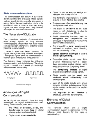
  • 1. Digital communication systems The communication that occurs in our day-to- day life is in the form of signals. These signals, such as sound signals, generally, are analog in nature. When the communication needs to be established over a distance, then the analog signals are sent through wire, using different techniques for effective transmission. The Necessity of Digitization The conventional methods of communication used analog signals for long distance communications, which suffer from many losses such as distortion, interference, and other losses including security breach. In order to overcome these problems, the signals are digitized using different techniques. The digitized signals allow the communication to be more clear and accurate without losses. The following figure indicates the difference between analog and digital signals. The digital signals consist of 1s and 0s which indicate High and Low values respectively. Advantages of Digital Communication As the signals are digitized, there are many advantages of digital communication over analog communication, such as −  The effect of distortion, noise, and interference is much less in digital signals as they are less affected.  Digital circuits are more reliable.  Digital circuits are easy to design and cheaper than analog circuits.  The hardware implementation in digital circuits, is more flexible than analog.  The occurrence of cross-talk is very rare in digital communication.  The signal is un-altered as the pulse needs a high disturbance to alter its properties, which is very difficult.  Signal processing functions such as encryption and compression are employed in digital circuits to maintain the secrecy of the information.  The probability of error occurrence is reduced by employing error detecting and error correcting codes.  Spread spectrum technique is used to avoid signal jamming.  Combining digital signals using Time Division Multiplexing TDM is easier than combining analog signals using Frequency Division Multiplexing FDM.  The configuring process of digital signals is easier than analog signals.  Digital signals can be saved and retrieved more conveniently than analog signals.  Many of the digital circuits have almost common encoding techniques and hence similar devices can be used for a number of purposes.  The capacity of the channel is effectively utilized by digital signals. Elements of Digital Communication The elements which form a digital communication system is represented by the following block diagram for the ease of understanding.
  • 2. Following are the sections of the digital communication system. Source The source can be an analog signal. Example: A Sound signal Input Transducer This is a transducer which takes a physical input and converts it to an electrical signal (Example: microphone). This block also consists of an analog to digital converter where a digital signal is needed for further processes. A digital signal is generally represented by a binary sequence. Source Encoder The source encoder compresses the data into minimum number of bits. This process helps in effective utilization of the bandwidth. It removes the redundant bits unnecessary excess bits,i.e.,zeroes Channel Encoder The channel encoder, does the coding for error correction. During the transmission of the signal, due to the noise in the channel, the signal may get altered and hence to avoid this, the channel encoder adds some redundant bits to the transmitted data. These are the error correcting bits. Digital Modulator The signal to be transmitted is modulated here by a carrier. The signal is also converted to analog from the digital sequence, in order to make it travel through the channel or medium. Channel The channel or a medium, allows the analog signal to transmit from the transmitter end to the receiver end. Digital Demodulator This is the first step at the receiver end. The received signal is demodulated as well as converted again from analog to digital. The signal gets reconstructed here. Channel Decoder The channel decoder, after detecting the sequence, does some error corrections. The distortions which might occur during the transmission, are corrected by adding some redundant bits. This addition of bits helps in the complete recovery of the original signal. Source Decoder The resultant signal is once again digitized by sampling and quantizing so that the pure digital output is obtained without the loss of information. The source decoder recreates the source output. Output Transducer This is the last block which converts the signal into the original physical form, which was at the input of the transmitter. It converts the electrical signal into physical output (Example: loud speaker). Output Signal This is the output which is produced after the whole process. Example − The sound signal received. sampling Sampling is defined as, “The process of measuring the instantaneous values of continuous-time signal in a discrete form.” Sample is a piece of data taken from the whole data which is continuous in the time domain. When a source generates an analog signal and if that has to be digitized, having 1s and 0s i.e., High or Low, the signal has to be discretized in
  • 3. time. This discretization of analog signal is called as Sampling. The following figure indicates a continuous-time signal x tt and a sampled signal xs tt. When x tt is multiplied by a periodic impulse train, the sampled signal xs tt is obtained. Sampling Rate To discretize the signals, the gap between the samples should be fixed. That gap can be termed as a sampling period Ts. SamplingFrequency=1/Ts=fs Where,  Ts is the sampling time  fs is the sampling frequency or the sampling rate Sampling frequency is the reciprocal of the sampling period. This sampling frequency, can be simply called as Sampling rate. The sampling rate denotes the number of samples taken per second, or for a finite set of values. For an analog signal to be reconstructed from the digitized signal, the sampling rate should be highly considered. The rate of sampling should be such that the data in the message signal should neither be lost nor it should get over- lapped. Hence, a rate was fixed for this, called as Nyquist rate. Nyquist Rate Suppose that a signal is band-limited with no frequency components higher than W Hertz. That means, W is the highest frequency. For such a signal, for effective reproduction of the original signal, the sampling rate should be twice the highest frequency. Which means, fS=2W Where,  fS is the sampling rate  W is the highest frequency This rate of sampling is called as Nyquist rate. A theorem called, Sampling Theorem, was stated on the theory of this Nyquist rate. Sampling Theorem The sampling theorem, which is also called as Nyquist theorem, delivers the theory of sufficient sample rate in terms of bandwidth for the class of functions that are bandlimited. The sampling theorem states that, “a signal can be exactly reproduced if it is sampled at the rate fs which is greater than twice the maximum frequency W.” To understand this sampling theorem, let us consider a band-limited signal, i.e., a signal whose value is non-zero between some – W and W Hertz. Such a signal is represented as x(f)=0 for|f|>W For the continuous-time signal x tt, the band- limited signal in frequency domain, can be represented as shown in the following figure. We need a sampling frequency, a frequency at which there should be no loss of information, even after sampling. For this, we have the Nyquist rate that the sampling frequency should
  • 4. be two times the maximum frequency. It is the critical rate of sampling. If the signal xtt is sampled above the Nyquist rate, the original signal can be recovered, and if it is sampled below the Nyquist rate, the signal cannot be recovered. The following figure explains a signal, if sampled at a higher rate than 2w in the frequency domain. The above figure shows the Fourier transform of a signal xs(t). Here, the information is reproduced without any loss. There is no mixing up and hence recovery is possible. The Fourier Transform of the signal xs(t) is Xs(w)=1/Ts∑n=−∞ to ∞X(w−nw0) Where Ts = Sampling Period and w0=2πTs Let us see what happens if the sampling rate is equal to twice the highest frequency (2W) That means, fs=2W Where,  fs is the sampling frequency  W is the highest frequency The result will be as shown in the above figure. The information is replaced without any loss. Hence, this is also a good sampling rate. Now, let us look at the condition, fs<2W The resultant pattern will look like the following figure. We can observe from the above pattern that the over-lapping of information is done, which leads to mixing up and loss of information. This unwanted phenomenon of over-lapping is called as Aliasing. Aliasing Aliasing can be referred to as “the phenomenon of a high-frequency component in the spectrum of a signal, taking on the identity of a low- frequency component in the spectrum of its sampled version.” The corrective measures taken to reduce the effect of Aliasing are −  In the transmitter section of PCM, a low pass anti-aliasing filter is employed, before the sampler, to eliminate the high frequency components, which are unwanted.  The signal which is sampled after filtering, is sampled at a rate slightly higher than the Nyquist rate. This choice of having the sampling rate higher than Nyquist rate,also helps in the easier design of the reconstruction filter at the receiver. Scope of Fourier Transform It is generally observed that, we seek the help of Fourier series and Fourier transforms in analyzing the signals and also in proving theorems. It is because −
  • 5.  The Fourier Transform is the extension of Fourier series for non-periodic signals.  Fourier transform is a powerful mathematical tool which helps to view the signals in different domains and helps to analyze the signals easily.  Any signal can be decomposed in terms of sum of sines and cosines using this Fourier transform. The digitization of analog signals involves the rounding off of the values which are approximately equal to the analog values. The method of sampling chooses a few points on the analog signal and then these points are joined to round off the value to a near stabilized value. Such a process is called as Quantization. Quantizing an Analog Signal The analog-to-digital converters perform this type of function to create a series of digital values out of the given analog signal. The following figure represents an analog signal. This signal to get converted into digital, has to undergo sampling and quantizing. The quantizing of an analog signal is done by discretizing the signal with a number of quantization levels. Quantization is representing the sampled values of the amplitude by a finite set of levels, which means converting a continuous-amplitude sample into a discrete-time signal. The following figure shows how an analog signal gets quantized. The blue line represents analog signal while the brown one represents the quantized signal. Both sampling and quantization result in the loss of information. The quality of a Quantizer output depends upon the number of quantization levels used. The discrete amplitudes of the quantized output are called as representation levels or reconstruction levels. The spacing between the two adjacent representation levels is called a quantum or step-size. The following figure shows the resultant quantized signal which is the digital form for the given analog signal. This is also called as Stair-case waveform, in accordance with its shape. Types of Quantization There are two types of Quantization - Uniform Quantization and Non-uniform Quantization. The type of quantization in which the quantization levels are uniformly spaced is termed as a Uniform Quantization. The type of quantization in which the quantization levels are unequal and mostly the relation between them is logarithmic, is termed as a Non-uniform Quantization. There are two types of uniform quantization. They are Mid-Rise type and Mid-Tread type. The following figures represent the two types of uniform quantization.
  • 6. Figure 1 shows the mid-rise type and figure 2 shows the mid-tread type of uniform quantization.  The Mid-Rise type is so called because the origin lies in the middle of a raising part of the stair-case like graph. The quantization levels in this type are even in number.  The Mid-tread type is so called because the origin lies in the middle of a tread of the stair-case like graph. The quantization levels in this type are odd in number.  Both the mid-rise and mid-tread type of uniform quantizers are symmetric about the origin. Quantization Error For any system, during its functioning, there is always a difference in the values of its input and output. The processing of the system results in an error, which is the difference of those values. The difference between an input value and its quantized value is called a Quantization Error. A Quantizer is a logarithmic function that perform Quantization rounding off the value. An analog-to-digital converter (ADC) works as a quantizer. The following figure illustrates an example for a quantization error, indicating the difference between the original signal and the quantized signal. Quantization Noise It is a type of quantization error, which usually occurs in analog audio signal, while quantizing it to digital. For example, in music, the signals keep changing continuously, where a regularity is not found in errors. Such errors create a wideband noise called as Quantization Noise. Advantages of Non – Uniform Quantization : 1. Higher average signal to quantization noise power ratio than the uniform quantizer when the signal pdf is non uniform which is the case in many practical situation. 2. RMS value of the quantizer noise power of a non – uniform quantizer is substantially proportional to the sampled value and hence the effect of the quantizer noise is reduced. Companding in PCM The word Companding is a combination of Compressing and Expanding, which means that it does both. This is a non-linear technique used in PCM which compresses the data at the transmitter and expands the same data at the receiver. The effects of noise and crosstalk are reduced by using this technique.  Companding is the process of compression and then expansion. With companded system, the higher amplitude analog signals are compressed (amplified less
  • 7. than lower amplitude signals) prior to transmission and then expanded (amplified more than the lower amplitude signals) in the receiver. Fig. 1 Block diagram of Companded PCM system  Companding is used in pulse code modulation (PCM). The process involves decreasing the number of bits used to record the strongest (loudest) signals.  In the digital file format, companding improves the signal-to-noise ratio at reduced bit rates. For example, a 16-bit PCM signal may be converted to an eight- bit ".wav" or ".au" file.  µ-law companding is used for speech and music signals.  µ-law is used in North America and Japan.  The process of compression of the signal at the transmitter and expansion at the receiver is called as companding (compression and expansion).  In companding, the higheramplitude analogsignals are compressed preceding transmission and then expanded in the receiver.  Companding is performed with the help of three functional blocks, which are Compressor, Uniform quantizerand Expander and the diagram in shown below in the Fig1. Fig1. Compander Functional Blocks  The compressor will compressthe dynamic rangeof the signal so that high dynamic range signal can be passed through components of low dynamic range capability, the uniform quantizer will undergo the quantization process of the compressed signal and the lastly the expanderwill undergo expansion andinvert the compressionfunction to reconstruct the original signal.  The expander has complementary characteristics as that of compressor so that the compressor input is equal to expanderoutput in order to reproduce the signal at the receiver.  The Fig2 below illustrates the input-output characteristics and curves of the companding process, and it can be seen that companding has linearcharacteristics.  It helps in minimizing noise, distortion, interference and reduction in the levels of crosstalk.  Companding helps in improving the dynamic range of the communication systems.  Companding is used in telephony and other audio applications. 1. In companding, we convert the signal into digital domain non-linearly to achieve compression.
  • 8. 2. Here the weakersignals areamplifiedby largerfactors while the stronger signals are amplified by smallerfactors. 3. There are two types of companding: o μ-law companding o A-law companding A-law Companding Technique  Uniform quantization is achieved at A = 1, where the characteristic curve is linear and no compression is done.  A-law has mid-rise at the origin. Hence, it contains a non-zero value.  A-law companding is used for PCM telephone systems. µ-law Companding Technique  Uniform quantization is achieved at µ = 0, where the characteristic curve is linear and no compression is done.  µ-law has mid-tread at the origin. Hence, it contains a zero value. 4. The μ-law and A-law companding standards employ logarithm based functions to encodeaudio samples forISDN (Integrated Services Digital Network) digital telephony services by means of non- linear quantization. μ-law companding  It is used in North America and Japan.  It uses the fact that low amplitude of speech signal contain more information than high amplitude.  Hence we can use non-linear quantization.  μ-law encoder inputs 14bit samples and outputs 8 bit codewords.  Since encoder receives 14 bit signed input sample x, the input range is (-8192, +8191).  This input sample is normalised to the interval (-1, +1) using the following logarithmic expression: 8 bit code = sgn(x)(ln [1+μ|x|])/(ln [1+|μ|]) |x|<=1 Where sgn(x) = where μ=0 to 255.  The 8-bit codeword in (-1, 1) is then scaled to the range (-256, 255) using following format recommended by G.711 standard. Here, P represents the sign of the input sample. Bits S2, S1 and S0 are the segment code. Q3, Q2 and Q0 are the quantization code. Encoder:  The encoder determines the segment code by adding a bias of 33 to the absolute value of input sample.  Determining the bit position of the most significant one bit among bits 5 to 12 of the input and subtracting 5 from that position.  The 4 bit quantization code is set to 4 bits following the bit position determined in step b.  The encoder ignores the remaining bits of the input sample and inverts the code word at its output. Decoder:  The quantization code is multiplied by 2 and then the bias of 33 is added to the result.  The result of step a. is multiplied by 2SC where SC is segment code.  This result is decremented by a bias of 33.
  • 9.  The sign of the result is determined using bit P. A-law companding  The A-law compander has a midriser and is defined by  Encoder:  The A-law encoder inputs 13 bit samples and outputs 8 bit code words.  The range of signed input is (-4096, +4095) and this input sample x is normalised to interval (-1, 1) using logarithmic expression. 8 bit code = sgn(x) (A|x|)/(1+ln(A)) for0 ≤ |x|≤1/A =sgn(x) (1+ln(A|x|))/(1+ln(A)) for1/A ≤ |x| ≤ 1 This code word is then scaled to (-256, 255) using following format recommended by G.711 standard. P S1 S2 S0 Q3 Q2 Q1 Q0 The bit pattern P determines the sign of the input samples. The segment code is determined as A) Determine the bit position of the most significant bit in the input. B) If such a position is found, the segment code becomes the position determined in step a. minus 4 otherwise it becomes 0. C) The 4 bit QC is set to the 4 bits following the bit position determined in step a. or half of the input value if the segment code is 0. D) The encoder ignores the remaining bits of the input sample and it inverts the bit P and the even numbered bits of the code word bit it is output. Decoder: A) It inverts bit P and the even numbered bits of the code. B) If the segment code is non-zero, the decoder multiplies the quantization code by 2 and increments this by a bias of 33. This result is then multiplied by 2SC – 1. C) Bit P is used to determine the sign of the output sample. Pulse Code Modulation Modulation is the process of varying one or more parameters of a carrier signal in accordance with the instantaneous values of the message signal. The message signal is the signal which is being transmitted for communication and the carrier signal is a high frequency signal which has no data, but is used for long distance transmission. There are many modulation techniques, which are classified according to the type of modulation employed. Of them all, the digital modulation technique used is Pulse Code Modulation PCM. A signal is pulse code modulated to convert its analog information into a binary sequence, i.e., 1s and 0s. The output of a PCM will resemble a binary sequence. The following figure shows an example of PCM output with respect to instantaneous values of a given sine wave.
  • 10. Instead of a pulse train, PCM produces a series of numbers or digits, and hence this process is called as digital. Each one of these digits, though in binary code, represent the approximate amplitude of the signal sample at that instant. In Pulse Code Modulation, the message signal is represented by a sequence of coded pulses. This message signal is achieved by representing the signal in discrete form in both time and amplitude. Basic Elements of PCM The transmitter section of a Pulse Code Modulator circuit consists of Sampling, Quantizing and Encoding, which are performed in the analog-to-digital converter section. The low pass filter prior to sampling prevents aliasing of the message signal. The basic operations in the receiver section are regeneration of impaired signals, decoding, and reconstruction of the quantized pulse train. Following is the block diagram of PCM which represents the basic elements of both the transmitter and the receiver sections. Low Pass Filter This filter eliminates the high frequency components present in the input analog signal which is greater than the highest frequency of the message signal, to avoid aliasing of the message signal. Sampler This is the technique which helps to collect the sample data at instantaneous values of message signal, so as to reconstruct the original signal. The sampling rate must be greater than twice the highest frequency component W of the message signal, in accordance with the sampling theorem. Quantizer Quantizing is a process of reducing the excessive bits and confining the data. The sampled output when given to Quantizer, reduces the redundant bits and compresses the value. Encoder The digitization of analog signal is done by the encoder. It designates each quantized level by a binary code. The sampling done here is the sample-and-hold process. These three sections LPF,Sampler,andQuantizer will act as an analog to digital converter. Encoding minimizes the bandwidth used. Regenerative Repeater This section increases the signal strength. The output of the channel also has one regenerative repeater circuit, to compensate the signal loss and reconstruct the signal, and also to increase its strength. Decoder The decoder circuit decodes the pulse coded waveform to reproduce the original signal. This circuit acts as the demodulator. Reconstruction Filter After the digital-to-analog conversion is done by the regenerative circuit and the decoder, a low- pass filter is employed, called as the reconstruction filter to get back the original signal. Hence, the Pulse Code Modulator circuit digitizes the given analog signal, codes it and samples it, and then transmits it in an analog form. This whole process is repeated in a reverse pattern to obtain the original signal.
  • 11. LINE CODING IN DIGITAL COMMUNICATION >> WHAT IS LINE CODING? In telecommunication, a line code (also called digital baseband modulation, also called digital baseband transmission method) is a code chosen for use within a communications system for baseband transmission purposes. Line coding is often used for digital data transport. Binary 1’s and 0’s, such as in PCM signaling, may be represented in various serial–bit signaling formats called line codes. WHY LINE CODING? There are many reasons for using line coding. Each of the line codes you will be examining offers one or more of the following advantages:  Spectrum Shaping and Relocation without modulation or filtering. This is important in telephone line applications, for example, where the transfer characteristic has heavy attenuation below 300 Hz.  Bit clock recovery can be simplified.  DC component can be eliminated; this allows AC (capacitor or transformer) coupling between stages (as in telephone lines). Can control baseline wander (baseline wander shifts the position of the signal waveform relative to the detector threshold and leads to severe erosion of noise margin).  Error detection capabilities.  Bandwidth usage; the possibility of transmitting at a higher rate than other schemes over the same bandwidth. At the very least the LINE-CODE ENCODER serves as an interface between the TTL level signals of the transmitter and those of the analog channel. Likewise, the LINE-CODE DECODER serves as an interface between the analog signals of the channel and the TTL level signals required by the digital receiver. >> MOST POPULAR LINE CODES Some of the most popular line codes are shown below.The line codes shown above are also known by other names: Polar NRZ: Also called NRZ–L where L denotes the normal logic level assignment Bipolar RZ: Also called RZ–AMI, where AMI denotes alternate mark (binary 1) inversion Bipolar NRZ: Also called NRZ–M, where M denotes inversion on mark (binary 1) A line code is the code used for data transmission of a digital signal over a transmission line. This process of coding is chosen so as to avoid overlap and distortion of signal such as inter-symbol interference. Properties of Line Coding Following are the properties of line coding −  As the coding is done to make more bits transmit on a single signal, the bandwidth used is much reduced.  For a given bandwidth, the power is efficiently used.  The probability of error is much reduced.  Error detection is done and the bipolar too has a correction capability.  Power density is much favorable.  The timing content is adequate.  Long strings of 1s and 0s is avoided to maintain transparency. Types of Line Coding There are 3 types of Line Coding  Unipolar  Polar  Bi-polar Unipolar Signaling
  • 12. Unipolar signaling is also called as On-Off Keying or simply OOK. The presence of pulse represents a 1 and the absence of pulse represents a 0. There are two variations in Unipolar signaling −  Non Return to Zero NRZ  Return to Zero RZ Unipolar Non-Return to Zero NRZ In this type of unipolar signaling, a High in data is represented by a positive pulse called as Mark, which has a duration T0 equal to the symbol bit duration. A Low in data input has no pulse. The following figure clearly depicts this. Advantages The advantages of Unipolar NRZ are −  It is simple.  A lesser bandwidth is required. Disadvantages The disadvantages of Unipolar NRZ are −  No error correction done.  Presence of low frequency components may cause the signal droop.  No clock is present.  Loss of synchronization is likely to occur (especially for long strings of 1s and 0s). Unipolar Return to Zero RZ In this type of unipolar signaling, a High in data, though represented by a Mark pulse, its duration T0 is less than the symbol bit duration. Half of the bit duration remains high but it immediately returns to zero and shows the absence of pulse during the remaining half of the bit duration. It is clearly understood with the help of the following figure. Advantages The advantages of Unipolar RZ are −  It is simple.  The spectral line present at the symbol rate can be used as a clock. Disadvantages The disadvantages of Unipolar RZ are −  No error correction.  Occupies twice the bandwidth as unipolar NRZ.  The signal droop is caused at the places where signal is non-zero at 0 Hz. Polar Signaling There are two methods of Polar Signaling. They are −  Polar NRZ  Polar RZ
  • 13. Polar NRZ In this type of Polar signaling, a High in data is represented by a positive pulse, while a Low in data is represented by a negative pulse. The following figure depicts this well. Advantages The advantages of Polar NRZ are −  It is simple.  No low-frequency components are present. Disadvantages The disadvantages of Polar NRZ are −  No error correction.  No clock is present.  The signal droop is caused at the places where the signal is non-zero at 0 Hz. Polar RZ In this type of Polar signaling, a High in data, though represented by a Mark pulse, its duration T0 is less than the symbol bit duration. Half of the bit duration remains high but it immediately returns to zero and shows the absence of pulse during the remaining half of the bit duration. However, for a Low input, a negative pulse represents the data, and the zero level remains same for the other half of the bit duration. The following figure depicts this clearly. Advantages The advantages of Polar RZ are −  It is simple.  No low-frequency components are present. Disadvantages The disadvantages of Polar RZ are −  No error correction.  No clock is present.  Occupies twice the bandwidth of Polar NRZ.  The signal droop is caused at places where the signal is non-zero at 0 Hz. Bipolar Signaling This is an encoding technique which has three voltage levels namely +, - and 0. Such a signal is called as duo-binary signal. An example of this type is Alternate Mark Inversion AMI. For a 1, the voltage level gets a transition from + to – or from – to +, having alternate 1s to be of equal polarity. A 0 will have a zero voltage level. Even in this method, we have two types.  Bipolar NRZ  Bipolar RZ From the models so far discussed, we have learnt the difference between NRZ and RZ. It just goes in the same way here too. The following figure clearly depicts this.
  • 14. The above figure has both the Bipolar NRZ and RZ waveforms. The pulse duration and symbol bit duration are equal in NRZ type, while the pulse duration is half of the symbol bit duration in RZ type. Advantages Following are the advantages −  It is simple.  No low-frequency components are present.  Occupies low bandwidth than unipolar and polar NRZ schemes.  This technique is suitable for transmission over AC coupled lines, as signal drooping doesn’t occur here.  A single error detection capability is present in this. Disadvantages Following are the disadvantages −  No clock is present.  Long strings of data causes loss of synchronization.
  • 15. >> DIFFERENTIAL CODING When serial data is passed through many circuits along a communication channel, the waveform is often unintentionally inverted (i.e. data complemented). This result can occur in a twisted pair transmission line channel just by switching the 2 leads at a connection point when a polar line code is used. (Note: such switching would not affect the data of a bipolar signal) To eliminate this problem differential encoding is often employed. Each digit in an differential encoded sequence is obtained by comparing the present input bit with the past encoded bit. A binary 1 is encoded if the present input bit and past encoded bit are of opposite state. A binary 0 is encoded if the states are the same. Differential coding is often used with Manchester coding. Differential pulse code modulation For the samples that are highly correlated, when encoded by PCM technique, leave redundant information behind. To process this redundant information and to have a better output, it is a wise decisionto take a predicted sampled value, assumed from its previous output and summarize them with the quantized values. Such a process is called as Differential PCM DPCMtechnique. DPCM Transmitter The DPCM Transmitter consists of Quantizer and Predictor with two summer circuits. Following is the block diagram of DPCM transmitter. The signals at each point are named as −  x(nTs) is the sampled input  xˆ(nTs) is the predicted sample  e(nTs) is the difference of sampled input and predicted output, often called as prediction error  v(nTs)is the quantized output  u(nTs)is the predictor input which is actually the summer output of the predictor output and the quantizer output The predictor produces the assumed samples from the previous outputs of the transmitter
  • 16. circuit. The input to this predictor is the quantized versions of the input signal x(nTs). Quantizer Output is represented as − v(nTs)=Q[e(nTs)] =e(nTs)+q(nTs) =e(nTs)+q(nTs) Where q (nTs) is the quantization error Predictor input is the sum of quantizer output and predictor output, u(nTs)=xˆ(nTs)+v(nTs) u(nTs)=xˆ(nTs)+e(nTs)+q(nTs) u(nTs)=x(nTs)+q(nTs) The same predictor circuit is used in the decoder to reconstruct the original input. DPCM Receiver The block diagram of DPCM Receiver consists of a decoder, a predictor, and a summer circuit. Following is the diagram of DPCM Receiver. The notation of the signals is the same as the previous ones. In the absence of noise, the encoded receiver input will be the same as the encoded transmitter output. As mentioned before, the predictor assumes a value, based on the previous outputs. The input given to the decoder is processed and that output is summed up with the output of the predictor, to obtain a better output. Prediction gain: Adaptive differential pulse code modulation:
  • 17. Time division multiplexing TDM is the time interleaving of samples from several sources so that the information from these sources can be transmitted serially over a single communication channel. At the receiver the decommutator (sampler) has to be synchronized with the incoming waveform so that the PAM samples corresponding to source-1 will appear on the channel-1 output. Synchronisation Frame synchronization is needed at the TDM receiver so that the received multiplexed data can be sorted and directed to appropriate output channel. Frame sync is provided to the receiver in two different ways: >> provided to the de-multiplexer circuit by sending a frame sync signal from the transmitter over a separate channel >> derive the frame sync from the TDM signal itself Figure show that frame sync can be multiplexed along with the information words in an N channel TDM system.
  • 18. Figure shows that the frame sync is recovered from the corrupted TDM signal by using a frame synchronizer circuit which crosscorrelates the regenerated TDM signal with the expected unique sync word vector s = (s1,s2,…,sK). Multiplexing Multiplexing is the process of combining multiple signals into one signal, over a shared medium. These signals, if analog in nature, the process is called as analog multiplexing. If digital signals are multiplexed, it is called as digital multiplexing. Multiplexing was first developed in telephony. A number of signals were combined to send through a single cable. The process of multiplexing divides a communication channel into several number of logical channels, allotting each one for a different message signal or a data stream to be transferred. The device that does multiplexing, can be called as a MUX. The reverse process, i.e., extracting the number of channels from one, which is done at the receiver is called as de-multiplexing. The device which does de-multiplexing is called as DEMUX. The following figures represent MUX and DEMUX. Their primary use is in the field of communications. Types of Multiplexers There are mainly two types of multiplexers, namely analog and digital. They are further divided into FDM, WDM, and TDM. The following figure gives a detailed idea on this classification. Actually, there are many types of multiplexing techniques. Of them all, we have the main types with general classification, mentioned in the above figure. Analog Multiplexing The analog multiplexing techniques involve signals which are analog in nature. The analog signals are multiplexed according to their frequency FDM or wavelength WDM. Frequency Division Multiplexing FDMFDM In analog multiplexing, the most used technique is Frequency Division Multiplexing FDM. This technique uses various frequencies to combine streams of data, for sending them on a communication medium, as a single signal. Example − A traditional television transmitter, which sends a number of channels through a single cable, uses FDM. Wavelength Division Multiplexing WDM Wavelength Division multiplexing is an analog technique, in which many data streams of different wavelengths are transmitted in the light spectrum. If the wavelength increases, the frequency of the signal decreases. A prism which can turn different wavelengths into a single line, can be used at the output of MUX and input of DEMUX. Example − Optical fiber communications use WDM technique to merge different wavelengths into a single light for communication.
  • 19. Digital Multiplexing The term digital represents the discrete bits of information. Hence, the available data is in the form of frames or packets, which are discrete. Time Division Multiplexing TDM In TDM, the time frame is divided into slots. This technique is used to transmit a signal over a single communication channel, by allotting one slot for each message. Of all the types of TDM, the main ones are Synchronous and Asynchronous TDM. Synchronous TDM In Synchronous TDM, the input is connected to a frame. If there are ‘n’ number of connections, then the frame is divided into ‘n’ time slots. One slot is allocated for each input line. In this technique, the sampling rate is common to all signals and hence the same clock input is given. The MUX allocates the same slot to each device at all times. Asynchronous TDM In Asynchronous TDM, the sampling rate is different for each of the signals and a common clock is not required. If the allotted device, for a time-slot, transmits nothing and sits idle, then that slot is allotted to another device, unlike synchronous. This type of TDM is used in Asynchronous transfer mode networks. Regenerative Repeater For any communication system to be reliable, it should transmit and receive the signals effectively, without any loss. A PCM wave, after transmitting through a channel, gets distorted due to the noise introduced by the channel. The regenerative pulse compared with the original and received pulse, will be as shown in the following figure. For a better reproduction of the signal, a circuit called as regenerative repeater is employed in the path before the receiver. This helps in restoring the signals from the losses occurred. Following is the diagrammatical representation. This consists of an equalizer along with an amplifier, a timing circuit, and a decision making device. Their working of each of the components is detailed as follows. Equalizer The channel produces amplitude and phase distortions to the signals. This is due to the transmission characteristics of the channel. The Equalizer circuit compensates these losses by shaping the received pulses. Timing Circuit To obtain a quality output, the sampling of the pulses should be done where the signal to noise ratio SNR is maximum. To achieve this perfect sampling, a periodic pulse train has to be derived from the received pulses, which is done by the timing circuit. Hence, the timing circuit, allots the timing interval for sampling at high SNR, through the received pulses.
  • 20. Decision Device The timing circuit determines the sampling times. The decision device is enabled at these sampling times. The decision device decides its output based on whether the amplitude of the quantized pulse and the noise, exceeds a pre- determined value or not. These are few of the techniques used in digital communications. There are other important techniques to be learned, called as data encoding techniques. Let us learn about them in the subsequent chapters, after taking a look at the line codes. Intro to delta modulation: The sampling rate of a signal should be higher than the Nyquist rate, to achieve better sampling. If this sampling interval in Differential PCM is reduced considerably, the sampleto- sample amplitude difference is very small, as if the difference is 1-bit quantization, then the step-size will be very small i.e., Δ deltadelta. Delta Modulation The type of modulation, where the sampling rate is much higher and in which the stepsize after quantization is of a smaller value Δ, such a modulation is termed as delta modulation. Features of Delta Modulation Following are some of the features of delta modulation.  An over-sampled input is taken to make full use of the signal correlation.  The quantization design is simple.  The input sequence is much higher than the Nyquist rate.  The quality is moderate.  The design of the modulator and the demodulator is simple.  The stair-case approximation of output waveform.  The step-size is very small, i.e., Δ delta.  The bit rate can be decided by the user.  This involves simpler implementation. Delta Modulation is a simplified form of DPCM technique, also viewed as 1-bit DPCM scheme. As the sampling interval is reduced, the signal correlation will be higher. Delta Modulator The Delta Modulator comprises of a 1-bit quantizer and a delay circuit along with two summer circuits. Following is the block diagram of a delta modulator. The predictor circuit in DPCM is replaced by a simple delay circuit in DM. From the above diagram, we have the notations as −  x(nTs) = over sampled input  ep(nTs) = summer output and quantizer input  eq(nTs)=quantizeroutput= v(nTs)  x^(nTs) = output of delay circuit  u(nTs) = input of delay circuit Using these notations, now we shall try to figure out the process of delta modulation. ep(nTs)=x(nTs)−xˆ(nTs) ----eqn 1 =x(nTs)−u([n−1]Ts) =x(nTs)−[xˆ[[n−1]Ts]+v[[n−1]Ts]]----eqn 2
  • 21. Further, v(nTs)=eq(nTs)=S.sig.[ep(nTs)]----eqn 3 u(nTs)=xˆ(nTs)+eq(nTs) Where,  xˆ(nTs) = the previous value of the delay circuit  eq(nTs)=quantizeroutput= v(nTs) Hence,u(nTs)=u([n−1]Ts)+v(nTs)----eqn 4 Which means, The present input of the delay unit = Thepreviousoutputofthedelayunit + thepresen tquantizeroutput Assuming zero condition of Accumulation, u(nTs)=S∑j=1tonsig[ep(jTs)] Accumulated version of DM output = ∑j=1tonv(jTs)----eqn 5 Now, note that xˆ(nTs)=u([n−1]Ts) xˆ(nTs)=∑j=1ton−1v(jTs)--eqn 6 Delay unit output is an Accumulator output lagging by one sample. From equations 5 & 6, we get a possible structure for the demodulator. A Stair-case approximated waveform will be the output of the delta modulator with the step-size as delta (Δ). The output quality of the waveform is moderate. Delta Demodulator The delta demodulator comprises of a low pass filter, a summer, and a delay circuit. The predictor circuit is eliminated here and hence no assumed input is given to the demodulator. Following is the diagram for delta demodulator. From the above diagram, we have the notations as −  vˆ(nTs) is the input sample  uˆ(nTs) is the summer output  x¯(nTs) is the delayed output A binary sequence will be given as an input to the demodulator. The stair-case approximated output is given to the LPF. Low pass filter is used for many reasons, but the prominent reason is noise elimination for out-of- band signals. The step-size error that may occur at the transmitter is called granular noise, which is eliminated here. If there is no noise present, then the modulator output equals the demodulator input. Advantages of DM Over DPCM  1-bit quantizer  Very easy designof the modulator and the demodulator However, there exists some noise in DM.  Slope Over load distortion (when Δ is small)  Granular noise (when Δ is large)
  • 22. Adaptive Delta Modulation ADM In digital modulation, we have come across certain problem of determining the step-size, which influences the quality of the output wave. A larger step-size is needed in the steep slope of modulating signal and a smaller stepsize is needed where the message has a small slope. The minute details get missed in the process. So, it would be better if we can control the adjustment of step-size, according to our requirement in order to obtain the sampling in a desired fashion. This is the concept of Adaptive Delta Modulation. Following is the block diagram of Adaptive delta modulator. The gain of the voltage controlled amplifier is adjusted by the output signal from the sampler. The amplifier gain determines the step-size and both are proportional. ADM quantizes the difference between the value of the current sample and the predicted value of the next sample. It uses a variable step height to predict the next values, for the faithful reproduction of the fast varying values.