1. ADVANCED MICRO ELECTRO MECHANICAL SYSTEMS, ELECTRONICSAND COMPUTER ENGINEERING, WESTERNMICHIGAN
UNIVERSITY.
1
Abstract— Accelerometers are usedto sense the acceleration of
a moving body and convert it into electrical ormechanical energy
so that it could be measured. MEMS (Microelectromechanical
Systems) refers to the technology integrating electrical and
mechanical components with feature size of 1~1000 microns. Air
bag controls uses very complex calculations to make air bag
deployment decisions basedon crash severity relatedto the change
in vehicle speed, due to this factor the air bag deployment during
a collision is not easily obtained. So we designed a capacitive
accelerometer to overcome this problem. In this project we
designed a dual axis capacitive accelerometer which measures
acceleration of a car in dual directions (X and Y). In this we have
a circuitry which converts capacitive change to voltage. The circuit
is fabricated on silicon on glass (SOG) technology which is
designedby (ED) NMOS technology. The output of that circuit is
given as the input to the control unit to activate the capacitive
sensor.
Index Terms—Micro electromechanical systems (MEMS),
Accelerometer, Operational Amplifier, Dual Axis Accelerometer.
I. INTRODUCTION (NAVEEN KAVVADI)
icro-Electro-Mechanical Systems, or MEMS, is a
technology that in its most general form can be defined
as miniaturized mechanical and electro-mechanical elements
(i.e., devices and structures)that are made using the techniques
of micro fabrication. The critical physical dimensions of
MEMS devices can vary from well below one micron on the
lower end of the dimensional spectrum, all the way to several
millimeters. Likewise, the types of MEMS devices can vary
from relatively simple structures having no moving elements,
to extremely complex electromechanical systems with multiple
moving elements under the control of integrated
microelectronics. The one main criterion of MEMS is that there
are at least some elements having some sort of mechanical
functionality whether or not these elements can move. The term
used to define MEMS varies in different parts of the world. In
the United States they are predominantly called MEMS, while
in some other parts of the world they are called “Microsystems
Technology” or “micro machined devices”.
A capacitive accelerometer is a type of acceleration device
that is used to measure the acceleration using capacitive sensing
techniques. It has the ability to sense static and dynamic
acceleration on a equipment or a device enforced human or
mechanical forces and converts this acceleration into electrical
currents or voltage. A capacitive accelerometer is a vibration
sensor.A capacitive accelerometer senses and records vibration
produced on a device or surface.
An accelerometer is a device that measures proper
acceleration. Proper acceleration is not the same as coordinate
acceleration (rate of change of velocity). For example, an
accelerometer at rest on the surface of the Earth will measure
an acceleration g=9.81 m/s2 straight upwards. By contrast,
accelerometers in free fall orbiting and accelerating due to the
gravity of Earth will measure zero.
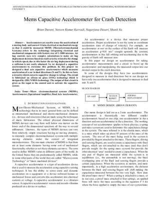
In this paper we design an accelerometer for taking
accelerometer measurements and a circuit to boost up the
accelerometer and manipulating the measured output into our
desired output in the crash detection.
In some of the designs they have two accelerometers
designed to measure in dual directions but in our design we
have only one accelerometer that is designed to measure in dual
axis X and Y.
BLOCK DIAGRAM
II. MEMS DESIGN (BRIAN DURANT)
Our mems design is laid out as a 2-axis accelerometer. The
accelerometer is theoretically two different smaller
accelerometers based on one chip, one accelerometer in the x
direction and one accelerometer in the y direction. The working
concept of our accelerometer applies to basic physics; a spring
and mass systemare used to determine the capacitance change
in the system. The mass referred to is the shuttle mass, which
is a mass which takes up about 85 percent of the mass of the
system. The rest of the mass being used in the system is
provided by fingers attached to the mass. These fingers, driving
and sensing fingers, are used to create a capacitance with fixed
fingers, which are not attached to the mass (and thus don’t
provide weight for the spring mass system) but provide the
otherelectrical ‘area’ needed to create a capacitance. When the
any pair of fingers are measured while the system is in
equilibrium (i.e., the automobile is not moving), the fixed
overlapping area of the fixed and sensing fingers provide a
certain capacitance. When the systemis in motion, and more
importantly, in a high acceleration environment, the distance
between the fixed and sensing fingers will shift making the
capacitance measured between the two very high. How does
the proof mass move? When a spring is attached to a mass, or
in our case, a proof mass attached to four springs, an applied
force will move the mass according to the equation 𝐹 = 𝑘𝑥
where the force applied is simply the mass of our systemtimes
Mems Capacitive Accelerometer for Crash Detection
Brian Durant, Naveen Kumar Kavvadi, Nagarjuna Dasari, Shunli Xu.
M
OP-AMP ACCELE
ROMET
ER
AIR BAG
DEPLOYMENT
2. ADVANCED MICRO ELECTRO MECHANICAL SYSTEMS, ELECTRONICSAND COMPUTER ENGINEERING, WESTERNMICHIGAN
UNIVERSITY.
2
the acceleration we’re at. K is the spring constant ofthe spring,
which is determined by the orientation of the system. Ideally,
you would want the spring constant in one direction to be much
strongerthan in the other direction so that your design doesn’t
have much movement in the wrong direction. The MEMS
device was designed to be able to sense small changes in
capacitance since it is used for safety in automobiles which is
very important as it is a matter of lives being saved. To achieve
high sensitivity, we had to make sure the springs would have a
decently low spring constant combined with the distance
between the fingers being decently big. This way the
capacitance could change drastically to show when an
automobile crash occurs,or rather, when a huge acceleration is
experienced by the accelerometer
A. Layout (BRIAN DURANT)
Final design of MEMS in coventorware
The layout of the MEMS design is laid at as a two axis
accelerometer (X axis and Y axis). Here the proof mass of
length 3.184E-04m and width (1.5E-03m) with 2.67E+01m)
fingers along each edge, alternating with 26.66 fixed fingers of
electrodes. Each sensing finger has a width of 5.00E-06m and
each fixed finger as a width of 5.00-06m same with the sensing
finger. Gap between the fixed and sensing finger small (d01) is
maintained at 4.00E-06m and the gap between the fixed and
sensing fingers big (d02) is maintained at 1.60E-05m.
Gap between the driving and sensing fingers is (d03)
maintained at 1.00E-05 same with the driving (d04)fingers and
the wall
Here the proof mass is suspended by four support beams
(springs) of length 5.88E-05 and width 3.00E-04.
B. Calculations (NAGARJUNA DASARI)
Acceleration Tolerance: Because our device contains a
single moving mass and measures bi-directionally, the gap
distance between the fingers is the movement limit for the
mass. The force caused by the acceleration will move the
mass a distance dependent on the spring constant of the
support beams.
F = ma = kx
F represents the force applied to a spring, m is the mass of the
shuttle mass, a is the acceleration, k represents the spring
constant,and xis the displacement of the mass from its center
equilibrium point.
Resting Capacitance: The capacitance between two fingers
with the basic equations
C = 𝜺 ∗ 𝑨/d
C represents capacitance, ∈ the permittivity, A the
overlapping area of fingers, and d the gap distance between
fingers.
Capacitance from 𝒅 𝟎𝟏 =
𝜺𝑳 𝑨
𝒅 𝟎𝟏
=
𝜺( 𝑳 𝒐𝒗𝒆𝒓𝒍𝒂𝒑∗𝑯 𝒇𝒊𝒏𝒈𝒆𝒓𝒔)
𝒅 𝟎𝟏
= 𝑪 𝒅 𝟎𝟏
=
169 pF
Capacitance from 𝒅 𝟎𝟐 =
𝜺𝑳 𝑨
𝒅 𝟎𝟐
=
𝜺( 𝑳 𝒐𝒗𝒆𝒓𝒍𝒂𝒑∗𝑯 𝒇𝒊𝒏𝒈𝒆𝒓𝒔)
𝒅 𝟎𝟐
= 𝑪 𝒅 𝟎𝟐
=
42 pF
General capacitance =
𝜺𝑳 𝑨
𝒅
= 𝑪 𝒅 𝟎𝟏
+ 𝑪 𝒅 𝟎𝟐
= 𝑪 𝒈𝒆𝒏𝒆𝒓𝒂𝒍
=169+42 = 211 pF
C. MEMS Design goals
When designing the MEMS chip, the first step was to define
our design goals. As stated before, we were creating an
accelerometer for use in automobile applications. The
accelerometer to be created should be two axis since in most
applications, a vehicle will be moving in two axis and not in the
third axis. For our design, we created an accelerometer which
was reactive to the x and y direction and unreactive in the z
direction. The first thing we had to find out for our design was
what kind of acceleration the accelerometer will be sensing for.
After some research we decided that the acceleration value
should be 5g, where g is the acceleration of gravity, or 9.81
m/s^2 . We also decided that to have a high sensitivity, we
would need a good amount of sensing fingers, driving fingers,
fixed fingers, and a decent enough gap to determine whether
there was a strong change in capacitance or not. The next
figures you will see are the specs of the accelerometer. Items
in gray stand for items whose value cannot change no matter
what. Items in blue are items whose value are chosen by the
3. ADVANCED MICRO ELECTRO MECHANICAL SYSTEMS, ELECTRONICSAND COMPUTER ENGINEERING, WESTERNMICHIGAN
UNIVERSITY.
3
creator. Items in orange are items whose value changes
according to the value of items in gray and blue. The values of
the items in blue, namely, the number of springs, the length of
a sensing finger, the length of a fixed finger, the length of a
driving finger, the length of the proof mass, the length of a
spring element, the width of a sensing finger, the width of a
fixed finger, the width of a driving finger, the width of a proof
mass, the gap between the fixed and sensing fingers small, the
gap between the fixed and sensing fingers big, the gap between
the driving and sensing finger, the gap between the driving
finger and the wall, and the overlap length of the fixed and
sensing fingers are all determined by the creator in an attempt
to create the proper capacitance gain between the fingers. By
varying the length and width of fingers and the proof mass, you
are also changing the mass of the spring-mass system. By
varying the length and width of the spring as well as its
orientation, you are changing the spring constant of the spring
and thus changing how stiff the spring is. The stiffer the spring
is (i.g., the higher the spring constant),the less the mass would
be able to move so we had to make sure we didn’t make the
spring constant too high. Likewise, if the spring was too lax
(i.g, the lower the spring constant),the device would move too
much and short circuit a lot, rendering it useless and potentially
physically harming the systembefore its even made use of. To
prevent this, we ended up using a spring constant of one for
simplicity. The way we achieved this was by using a spring
whose spring constant would be one under certain conditions
which were easy to implement.
D. SOG PROCESS
(1) We etch the glass substrate by using photolithography
technology.
(2) A chrome layer (metal layer) is deposited across the entire
wafer, since a lift-off technique will be used to reveal the
bottom electrode.
(3) Deposit silicon.
(4) Deposit and wet etch Al.
(5) Finally wafer is DRIE etched to define the proof mass and
fingers
4. ADVANCED MICRO ELECTRO MECHANICAL SYSTEMS, ELECTRONICSAND COMPUTER ENGINEERING, WESTERNMICHIGAN
UNIVERSITY.
4
In order to create these MEMS devices, the SOG (silicon on
glass)process was used. This process which was used for every
MEMS device this year uses four masks. With the first mask,
we etch the glass with chrome and photoresist. Chrome is an
element on the periodic table that is used in etching due to its
properties. Photoresist is a material that changes properties
according to the amount of light that it is exposed to. In terms
of MEMS, photoresist allows for very accurate etching by
placement in regions where etching is either needed or not
needed (positive or negative photoresist). Photoresist etches
best in UV light so UV light is used in the process. In the case
of our MEMS project, the photoresist protects whatever is
under it, to prevent it from being etched. The next mask that is
used for the MEMS project is used to deposit the bottom
electrode, which is very important in establishing metal
connections that are used to read capacitance from the
respective proofmasses. The process used at this point is called
lift off, which is actually the exact opposite ofwhat the previous
step does. Instead of protection by photoresist, photoresist is
used as a sacrificial layer. Photoresist is deposited where
electrodes shouldn’t be used. Next, the electrode material is
placed down and the wafer is subject to photoresist removal
which will take the photoresist and anything on top of it away.
This makes sure you only have the desired electrode pattern left.
The third step in this process is wafer bonding. A 100
micrometer thick silicon wafer is bonded to the glass and 5000
angstroms of aluminum is deposited on top of the silicon to
create electrical contacts. The third mask etches the aluminum
away to form the metal contacts while the fourth mask called
DRIE (deep reactive ion etching) is used to etch the silicon to
the desired patterning. After designing our MEMS chip, we
created a process file which included all the etching, keeping in
mind positive and negative photoresists for masks so that our
accelerometer could be completed. What follows is the actual
simulated project results when masks were applied.
E. MEMS Testing (SHUNLI XU)
1. MEMS PART:
We loaded the SOG wafer on the probe station, before we
started to do the SOG testing,we used an ohmmeter to do short
circuit testing to make sure that some parts were short.
1) (a) MEASURE CAPACITANCE WITHOUT
ACCELERATION:
Here is the SOG wafer we used to do the testing.
(1.a.1) Fabricated MEMS Part
After we finished the short circuit testing,we began to measure
the capacitance, and connected two pads,one is for spring and
proof mass, and another is for capacitance region.
Here is the capacitance we got at X-axis and Y-axis without
acceleration:
C1=169pF
C2=42pF
2) (b) APPLY VOLTAGE TO DRIVING FINGERS TO
MAKE PROOFMASS MOVE:
After successfully measuring the capacitance, we applied
voltages (-30V to +30V) to the driving fingers, we used
Parameter Analyzer to get the CV curve.
Here are the capacitances at different voltages in X-axis and Y-
axis.
X-axis:
5. ADVANCED MICRO ELECTRO MECHANICAL SYSTEMS, ELECTRONICSAND COMPUTER ENGINEERING, WESTERNMICHIGAN
UNIVERSITY.
5
3) Graph for the table (1.b.1):
Y-axis:
4) Graph for the table(1.b.3):
From the figures we got from Parameter Analyzer, we find that
the capacitance didn't change so much at different voltages,
which are far away from our thoughts before the testing,I find
out some reasons for this problem:
1) The voltage issue: I think the minimum voltage to make the
proof mass move is more than ±30V, it means the voltage we
used to the proof mass is not enough.
2) The fabrication issue: During the fabrication, some mistakes
might be made that the proof mass was connected to some fixed
regions, it could be a reason that proof mass couldn't move and
also capacitance didn't change.
3) Spring issue:The spring constant might be too large to make
the proof mass move.
(c) SUMMARY AND CONCLUSION OF MEMS TESTING
PART
In this part,we didn't do the fabrication, and time is also limited,
we didn't get enough time to check our thoughts about the
errors, the capacitance we measured without acceleration is
much larger than our calculations, only the capacitance from
Parameter Analyzer is close to our calculations.
2. EDNMOS TESTING PART:
(a) SHORT CIRCUIT TEST:
Before we began the EDNMOS Test, we connected two short
pads to make sure those regions were short.
6. ADVANCED MICRO ELECTRO MECHANICAL SYSTEMS, ELECTRONICSAND COMPUTER ENGINEERING, WESTERNMICHIGAN
UNIVERSITY.
6
(2.a.1) Fabricated EDNMOS Part
5) (b) CIRCUIT SIMULATION IN LTSPICE:
We did the simulation in LT spice before we started the
EDNMOS Testing
The input is a sine wave (-90mV to +90mV):
(2.b.2)
The output in simulation:
(2.b.3)
6) (c) CIRCUIT TESTING:
After we knew the ideal input and output, we began to do the
testing. We also made the input as a since wave similar to the
simulation.
Here is the result:
(2.b.4) Input voltage
(2.b.5) Output voltage
7) (d) SUMMARY AND CONCLUSION OF EDNMOS
TESTING PART:
In this part, we just measured the output,but it didn't match our
result in LT spice, and I searched for the reason, and I find that
maybe the input's frequency was too large, I think if we reduce
the frequency, the output should satisfy our simulation, but the
value of output is 2.0V, it is similar to our simulation.
7. ADVANCED MICRO ELECTRO MECHANICAL SYSTEMS, ELECTRONICSAND COMPUTER ENGINEERING, WESTERNMICHIGAN
UNIVERSITY.
7
8) 3. EDNMOS TEST DIE:
Fabricated Test Die
In this part, we measured resistance, threshold voltages, 19-
Stage Oscillator Period, inverter's Vol and Voh.
9) (a) Resistance:
10) (b) Breakdown voltage:
Since in lecture I got some information’s about measuring
breakdown voltage,we need to use a diode, then we can get IV
curve of the diode,when the negative current goes down rapidly
,that the voltage is breakdown voltage.
(3.b.1)
But I connected capacitor to a diode, I found that there was no
current, it means the method I got from lectures cannot be used.
Therefore, I come up with a new idea, that I can increase the
voltage from 0V to a very large voltage, when the capacitor
stops working, we will get the breakdown voltage.
F. (c) Threshold voltage:
G.
Method:We grounded the source, and made the VBB=0V, and
change the Vg's value, got Id ,at last, we got Vg/Id curve to get
the threshold voltage.
Vt (Enhancement16/6):
Parameter from Parameter Analyzer:
9. ADVANCED MICRO ELECTRO MECHANICAL SYSTEMS, ELECTRONICSAND COMPUTER ENGINEERING, WESTERNMICHIGAN
UNIVERSITY.
9
(3.c.4)
Graph from (3.c.4):
(3.c.5)
Vt = 2.2V
Vt (Depletion 16/6):
Parameters:
(3.c.6)
In this part, the Id/Vg curve is a linear, that we couldn't get the
threshold voltage, and I think we should try to make Vg
negative, since depletion's threshold voltage may be negative.
VBB to get Vt-Enhancement (16/6) of 0.8V:
The way to get the VBB, I tried to use VBB at different values
(-+1V,-+2V,-+3V,-+5V,-+15V), but I still didn't get the Vt-
Enhancement (16/6) =0.8V, so, it may need me to use larger
voltages to make Vt-Enhancement (16/6) =0.8V.
19-Stage Ring Oscillator Period:
Use equation (1) and (2) to get the period:
..... (1)
..... (2)
tPLH and tphl can be determined from
(3.c.7)
After we got T, then F=1/T.
Inverter:
Vol (voltage output low) is given by VIh (voltage input high)
10. ADVANCED MICRO ELECTRO MECHANICAL SYSTEMS, ELECTRONICSAND COMPUTER ENGINEERING, WESTERNMICHIGAN
UNIVERSITY.
10
Voh (voltage output high) is given by VIL (voltage input low)
So, Vol=VIh,
Voh=VIL.
H. SUMMARY AND CONCLUSION:
From this part, we knew some methods to measure the threshold
voltage and oscillator’s period and frequency, also inverter’s
Voh and Vol. However, time is limited, we didn’t get all the
parameters.
III. CIRCUIT DESIGN (NAVEEN KAVVADI)
A. OP AMP Block Diagram
The goal of an op amp is to be used as a amplifier. Its purpose
is to take the difference of the voltages provided by the
Wheatstone bridge and amplify that value. The output of this is
used to calculate the mass flow rate. The operational amplifier
design consists of four basic stages. They are differential
amplifier, the current mirror, gain stage and buffer stage.Here
we have designed an EDNMOS (Enhanced and Depletion)
mode NMOS to get the strong ones and also several of the
transistors to reduce space. In order to get the desired gain
output we designed the transistor sizes accordingly in all the
stages to get higher gain and stability. Important parameters to
be noticed while designing an op-amp is slew rate, settling time,
bandwidth, chip area, gain and noise.
Enhanced and depletion technology provides additional
flexibility and makes possible self-biased current source
devices, high resistance loads and simple up level shifters. We
are using this open loop feedback circuit to meet all the
requirements. All the transistors in the op-amp are biased so that
they could operate in saturation mode. The current mirror is
used to set a current and then mirror that current to the rest of
the circuit since every transistor should be in saturation region
it is important to be able to set and mirror the proper current. In
stage two consists of a differential amplifier input for positive
and negative inputs of the op amp. This stage provides a high
gain to the difference between inverting and non-inverting
amplifier. In the feed back stage the feedback will be given to
via a base transistorin orderto increase the bandwidth and gain.
In the cascade stage the outputofthe before stage will be driven
to the next stage to increase input output isolation. The final
stage adds more gain, lowers the output impedance and also
serves a buffer stage to lower the output resistance of the op-
amp.
Circuit diagram of an Op-Amp
M8 biased by current source M9. Level shifter (M8) drives a
cascade stage consisting of M10, M12, and M13. Device M11
is used as current source to increase the Trans conductance of
M10. Output consists of source follower M16 biased by a
current source M17 a depletion device is used for M16 to allow
sufficiently positive output voltage swings. M16 and M17
largely determines charging time of capacitive loads.
B. Input of op-amp
C. Output of op-amp
Adde
d pass
transis
tor
Diff
amp
Current
mirror
Gain
stage
Buffer
stage
11. ADVANCED MICRO ELECTRO MECHANICAL SYSTEMS, ELECTRONICSAND COMPUTER ENGINEERING, WESTERNMICHIGAN
UNIVERSITY.
11
Op amp simulation results
parameter Value
Input resistance Sufficiently
high
Maximum peak to peak voltage -0.5 to 2.7
Input voltage <1V
Gain 30db
Here we have given an input voltage of less than 1 V so we
should get an output of more than 1V since we are designed an
op-amp which amplifies so got a peak to peak voltage of -0.5 to
2.7 V. Errors in the output is because of the transistorsizes that
we haven’t chosen correctly so we didn’t got the exact sine
output. The gain of our circuit is 30db.
Final design of EDNMOS
IV. CONCLUSION
We have designed ourMEMS accelerometer along with the Op-
Amp circuit. We designed the circuit with E/D NMOS
technology. Testing has been done on each component
individually, to determine their behavior. We have done
everything as prescribed in the c tools but we have found some
errors after our design. Some of the errors which we found are
mostly in the MEMS design and also our EDNMOS circuit
didn’t work as expected so we suggest to take more care in the
design region and also in assigning the values forthe transistors.
ACKNOWLEDGMENT
We want to express our appreciation to Professor Massood
Zandi Atashbar for his assistance and support in helping us
understand the complexities behind our project. We also like to
thank T.A Sai Guruva Avuthu for his valuable suggestions and
assistance during Mems design and testing part.
REFERENCES
[1] https://www.asee.org/documents/zones/zone1/2008/stude
nt/ASEE12008_0050_paper.pdf
[2] http://cmosedu.com/jbaker/papers/talks/Multistage_Opam
p_Presentation.pdf
[3] http://www.iaeng.org/publication/IMECS2010/IMECS20
10_pp1413-1417.pdf
[4] http://en.wikipedia.org/wiki/Airbag
[5] http://en.wikipedia.org/wiki/Accelerometer
[6] J. Darmanin, I. Grech, E. Gatt, and O. Casha, ”Design of
a 2-axis MEMS accelerometer”, Electronics, Circuits and
Systems (ICECS), 2011 18th IEEE International
Conference vol., no., pp.268,271, 11-14 Dec. 2011