1. Lecture 26 26 - 1
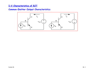
I-V Characteristics of BJT
Common-Emitter Output Characteristics
i B
B
C
E
C
i
CE
v
B
C
E
i B
C
i
EC
v
2. Lecture 26 26 - 2
To illustrate the IC-VCE characteristics, we use an enlarged βR
0 5 10
-5
-1
0
1
2
VCE (V)
Reverse-Active
Region
Saturation
Region
Cutoff
IB = 100 µA
IB = 80 µA
IB = 60 µA
IB = 40 µA
IB = 20 µA
IB = 0 µA
Forward Active
Region
Saturation
Region
βF = 25; βR = 5
Collector
Current
(mA)
vCE vBE
≥
iC βFiB
=
vCE vBE
≤
vCE vBE
≤
iC βR 1
+
( )
– iB
=
vCE vBE 0
≤ ≤
3. Lecture 26 26 - 3
Common Base Output Characteristics
iE
B
C
E
v
CB
C
i
B
C
E
v
BC
C
i
iE
4. Lecture 26 26 - 4
Forward-Active
Region
IE = 0 mA
IE = 0.2 mA
IE = 0.4 mA
IE = 0.6 mA
IE = 0.8 mA
IE = 1.0 mA
βF = 25; βR = 5
vCB or vBC (V)
-2 0 2 4 6 8 10
0
0.5
1.0
Collector
Current
(mA)
5. Lecture 26 26 - 5
Common-Emitter Transfer Characteristic iC - vBE
. BE voltage changes as -1.8 mV/oC - this is its temperature coef-
ficient (recall from diodes).
vBC = 0
Collector
Current
I
C
(mA)
-2
0
4
6
8
10
2
60 mV/decade
Base-Emitter Voltage (V)
0.0 0.2 0.4 0.6 0.8 1.0
10-11
10-9
10-8
10-6
10-4
10-2
Log(I
C
)
6. Lecture 26 26 - 6
Common-Emitter Transfer Characteristic iC - vBE (p. 180)
. BE voltage changes as -1.8 mV/oC - this is its temperature coef-
ficient (recall from diodes).
IC IS
vBE
VT
--------
-
1
–
exp
=
vBC = 0
Collector
Current
I
C
(mA)
-2
0
4
6
8
10
2
60 mV/decade
Base-Emitter Voltage (V)
0.0 0.2 0.4 0.6 0.8 1.0
10-11
10-9
10-8
10-6
10-4
10-2
Log(I
C
)
7. Lecture 26 26 - 7
Junction Breakdown - BJT has two diodes back-to-back. Each diode has a
breakdown. The diode (BE) with higher doping concentrations has the lower
breakdown voltage (5 to 10 V).
In forward active region, BC junction is reverse biased.
In cut-off region, BE and BC are both reverse biased.
The transistor must withstand these reverse bias voltages.
8. Lecture 26 26 - 8
Junction Breakdown - BJT has two diodes back-to-back. Each diode has a
breakdown. The diode (BE) with higher doping concentrations has the lower
breakdown voltage (5 to 10 V).
In forward active region, BC junction is reverse biased.
In cut-off region, BE and BC are both reverse biased.
The transistor must withstand these reverse bias voltages.
9. Lecture 26 26 - 9
Junction Breakdown - BJT has two diodes back-to-back. Each diode has a
breakdown. The diode (BE) with higher doping concentrations has the lower
breakdown voltage (5 to 10 V).
In forward active region, BC junction is reverse biased.
In cut-off region, BE and BC are both reverse biased.
The transistor must withstand these reverse bias voltages.
10. Lecture 26 26 - 10
Minority Carrier Transport in Base Region
Inj.
Elec.
recombined electrons
Coll.
Elec.
iT
IF/βF IR/βR
IREC
N P
N
Emitter Base Collector
Space Charge regions
(pno, npo)
+
- +
-
iE
iB
iC
vBE vBC
n(x)
x
n(WB)
WB
iT qADn
dn
dx
-----
-
=
n(0)
0
(pno, npo)
Electron conc.
in base (neglects
recombination)
Inj.
Holes
IREC
n 0
( ) nbo
vBE
VT
--------
-
exp
=
11. Lecture 26 26 - 11
Transport current iT results from diffusion of minority carriers (holes in npn)
across base region.
Base current iB is composed of holes injected back into E and C and IREC
needed to replenish holes lost to recombination with electrons in B.
The minority carrier concentrations at two ends of base are
and where is the equilib-
rium electron density in the base region.
The junction voltages establish a minority carrier concentration gradient at
ends of base region. For a narrow base, we get
is the B width; is the cross-sectional area of B region.
The saturation current is
nbo
WB A
12. Lecture 26 26 - 12
Transport current iT results from diffusion of minority carriers (electrons in
npn) across base region.
Base current iB is composed of holes injected back into E and C and IREC
needed to replenish holes lost to recombination with electrons in B.
The minority carrier concentrations at two ends of base are
and where is the equilib-
rium electron density in the base region.
The junction voltages establish a minority carrier concentration gradient at
ends of base region. For a narrow base, we get
is the B width; is the cross-sectional area of B region.
The saturation current is
n 0
( ) nbo
vBE
VT
---------
exp
= n WB
( ) nbo
vBC
VT
---------
exp
= nbo
WB A
13. Lecture 26 26 - 13
Transport current iT results from diffusion of minority carriers (holes in npn)
across base region.
Base current iB is composed of holes injected back into E and C and IREC
needed to replenish holes lost to recombination with electrons in B.
The minority carrier concentrations at two ends of base are
and where is the equilib-
rium electron density in the base region.
The junction voltages establish a minority carrier concentration gradient at
ends of base region. For a narrow base, we get
.
is the B width; is the cross-sectional area of B region.
The saturation current is
n 0
( ) nbo
vBE
VT
---------
exp
= n WB
( ) nbo
vBC
VT
---------
exp
= nbo
iT qADn
dn
dx
-----
- qADn
nbo
WB
--------
vBE
VT
---------
vBC
VT
---------
exp
–
exp
–
= =
WB A
14. Lecture 26 26 - 14
Transport current iT results from diffusion of minority carriers (holes in npn)
across base region.
Base current iB is composed of holes injected back into E and C and IREC
needed to replenish holes lost to recombination with electrons in B.
The minority carrier concentrations at two ends of base are
and where is the equilib-
rium electron density in the base region.
The junction voltages establish a minority carrier concentration gradient at
ends of base region. For a narrow base, we get
.
is the B width; is the cross-sectional area of B region.
The saturation current is .
n 0
( ) nbo
vBE
VT
---------
exp
= n WB
( ) nbo
vBC
VT
---------
exp
= nbo
iT qADn
dn
dx
-----
- qADn
nbo
WB
--------
vBE
VT
---------
vBC
VT
---------
exp
–
exp
–
= =
WB A
IS qADn
nbo
WB
-------- qADn
ni
2
NABW
B
--------------------
= =
15. Lecture 26 26 - 15
Base Transit Time
Forward transit time is time associated with storing charge Q in Base region
and it is
with .
Using we get
τF
Q
iT
----
= Q qA n 0
( ) nbo
–
[ ]
WB
2
--------
=
Q qAnbo
vBE
VT
---------
1
–
exp
WB
2
--------
=
16. Lecture 26 26 - 16
Using we get
and .
Q
n(x)
x
nbo
n(0)
n(WB) = nbo
0 WB
Q = excess minority
charge in Base
Q qAnbo
vBE
VT
---------
1
–
exp
WB
2
--------
=
iT
qADn
WB
--------------
-nbo
vBE
VT
---------
1
–
exp
= τF
WB
2
2Dn
---------
-
WB
2
2VTµ
n
----------------
-
= =
17. Lecture 26 26 - 17
This defines an upper limit on frequency .
f
1
2πτF
------------
-
≤
Q
n(x)
x
nbo
n(0)
n(WB) = nbo
0 WB
Q = excess minority
charge in Base
18. Lecture 26 26 - 18
PSPICE EXAMPLE
*Libraries:
* Local Libraries :
.LIB ".example10.lib"
* From [PSPICE NETLIST] section of C:Program FilesOrcadLitePSpicePSpice.ini file:
.lib "nom.lib"
*Analysis directives:
.DC LIN V_V1 0 5 0.05
+ LIN I_I1 10u 100u 10u
.PROBE V(*) I(*) W(*) D(*) NOISE(*)
.INC ".example10-SCHEMATIC1.net"
**** INCLUDING example10-SCHEMATIC1.net ****
* source EXAMPLE10
Q1 V1
0Vdc
BF=100
I1
0Adc
IS=1.0e-15
VAF=80
19. Lecture 26 26 - 19
PSPICE EXAMPLE (Cont’d)
Q_Q1 N00060 N00159 0 Qbreakn
V_V1 N00060 0 0Vdc
I_I1 0 N00159 DC 0Adc
**** RESUMING example10-SCHEMATIC1-Example10Profile.sim.cir ****
.END
**** BJT MODEL PARAMETERS
******************************************************************************
Qbreakn
NPN
IS 1.000000E-15
BF 100
NF 1
VAF 80
BR 3
NR 1
VAR 30
CN 2.42
D .87
JOB CONCLUDED
TOTAL JOB TIME .21