
Recommended
Recommended
More Related Content
What's hot
What's hot (18)
Similar to BPW34 – BPW34S - Datasheet - VISHAY
Similar to BPW34 – BPW34S - Datasheet - VISHAY (20)
More from MarioFarias18
More from MarioFarias18 (11)
Recently uploaded
Recently uploaded (20)
BPW34 – BPW34S - Datasheet - VISHAY
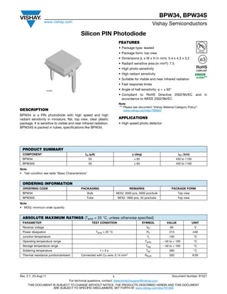
- 1. BPW34, BPW34S www.vishay.com Vishay Semiconductors Rev. 2.1, 23-Aug-11 1 Document Number: 81521 For technical questions, contact: detectortechsupport@vishay.com THIS DOCUMENT IS SUBJECT TO CHANGE WITHOUT NOTICE. THE PRODUCTS DESCRIBED HEREIN AND THIS DOCUMENT ARE SUBJECT TO SPECIFIC DISCLAIMERS, SET FORTH AT www.vishay.com/doc?91000 Silicon PIN Photodiode DESCRIPTION BPW34 is a PIN photodiode with high speed and high radiant sensitivity in miniature, flat, top view, clear plastic package. It is sensitive to visible and near infrared radiation. BPW34S is packed in tubes, specifications like BPW34. FEATURES • Package type: leaded • Package form: top view • Dimensions (L x W x H in mm): 5.4 x 4.3 x 3.2 • Radiant sensitive area (in mm2): 7.5 • High photo sensitivity • High radiant sensitivity • Suitable for visible and near infrared radiation • Fast response times • Angle of half sensitivity: ϕ = ± 65° • Compliant to RoHS Directive 2002/95/EC and in accordance to WEEE 2002/96/EC Note ** Please see document “Vishay Material Category Policy”: www.vishay.com/doc?99902 APPLICATIONS • High speed photo detector Note • Test condition see table “Basic Characteristics” Note • MOQ: minimum order quantity 94 8583 PRODUCT SUMMARY COMPONENT Ira (μA) ϕ (deg) λ0.1 (nm) BPW34 50 ± 65 430 to 1100 BPW34S 50 ± 65 430 to 1100 ORDERING INFORMATION ORDERING CODE PACKAGING REMARKS PACKAGE FORM BPW34 Bulk MOQ: 3000 pcs, 3000 pcs/bulk Top view BPW34S Tube MOQ: 1800 pcs, 45 pcs/tube Top view ABSOLUTE MAXIMUM RATINGS (Tamb = 25 °C, unless otherwise specified) PARAMETER TEST CONDITION SYMBOL VALUE UNIT Reverse voltage VR 60 V Power dissipation Tamb ≤ 25 °C PV 215 mW Junction temperature Tj 100 °C Operating temperature range Tamb - 40 to + 100 °C Storage temperature range Tstg - 40 to + 100 °C Soldering temperature t ≤ 3 s Tsd 260 °C Thermal resistance junction/ambient Connected with Cu wire, 0.14 mm2 RthJA 350 K/W
- 2. BPW34, BPW34S www.vishay.com Vishay Semiconductors Rev. 2.1, 23-Aug-11 2 Document Number: 81521 For technical questions, contact: detectortechsupport@vishay.com THIS DOCUMENT IS SUBJECT TO CHANGE WITHOUT NOTICE. THE PRODUCTS DESCRIBED HEREIN AND THIS DOCUMENT ARE SUBJECT TO SPECIFIC DISCLAIMERS, SET FORTH AT www.vishay.com/doc?91000 BASIC CHARACTERISTICS (Tamb = 25 °C, unless otherwise specified) Fig. 1 - Reverse Dark Current vs. Ambient Temperature Fig. 2 - Relative Reverse Light Current vs. Ambient Temperature BASIC CHARACTERISTICS (Tamb = 25 °C, unless otherwise specified) PARAMETER TEST CONDITION SYMBOL MIN. TYP. MAX. UNIT Breakdown voltage IR = 100 μA, E = 0 V(BR) 60 V Reverse dark current VR = 10 V, E = 0 Iro 2 30 nA Diode capacitance VR = 0 V, f = 1 MHz, E = 0 CD 70 pF VR = 3 V, f = 1 MHz, E = 0 CD 25 40 pF Open circuit voltage Ee = 1 mW/cm2, λ = 950 nm Vo 350 mV Temperature coefficient of Vo Ee = 1 mW/cm2, λ = 950 nm TKVo - 2.6 mV/K Short circuit current EA = 1 klx Ik 70 μA Ee = 1 mW/cm2, λ = 950 nm Ik 47 μA Temperature coefficient of Ik Ee = 1 mW/cm2, λ = 950 nm TKIk 0.1 %/K Reverse light current EA = 1 klx, VR = 5 V Ira 75 μA Ee = 1 mW/cm2, λ = 950 nm, VR = 5 V Ira 40 50 μA Angle of half sensitivity ϕ ± 65 deg Wavelength of peak sensitivity λp 900 nm Range of spectral bandwidth λ0.1 430 to 1100 nm Noise equivalent power VR = 10 V, λ = 950 nm NEP 4 x 10-14 W/√Hz Rise time VR = 10 V, RL = 1 kΩ, λ = 820 nm tr 100 ns Fall time VR = 10 V, RL = 1 kΩ, λ = 820 nm tf 100 ns 20 40 60 80 1 10 100 1000 100 94 8403 VR = 10 V Tamb - Ambient Temperature (°C) Iro-ReverseDarkCurrent(nA) 0.6 0.8 1.0 1.2 1.4 Ira,rel -RelativeReverseLightCurrent Tamb - Ambient Temperature (°C)94 8416 VR = 5 V λ = 950 nm 0 10080604020
- 3. BPW34, BPW34S www.vishay.com Vishay Semiconductors Rev. 2.1, 23-Aug-11 3 Document Number: 81521 For technical questions, contact: detectortechsupport@vishay.com THIS DOCUMENT IS SUBJECT TO CHANGE WITHOUT NOTICE. THE PRODUCTS DESCRIBED HEREIN AND THIS DOCUMENT ARE SUBJECT TO SPECIFIC DISCLAIMERS, SET FORTH AT www.vishay.com/doc?91000 Fig. 3 - Reverse Light Current vs. Irradiance Fig. 4 - Reverse Light Current vs. Illuminance Fig. 5 - Reverse Light Current vs. Reverse Voltage Fig. 6 - Diode Capacitance vs. Reverse Voltage Fig. 7 - Relative Spectral Sensitivity vs. Wavelength Fig. 8 - Relative Radiant Sensitivity vs. Angular Displacement 0.01 0.1 1 0.1 1 10 100 1000 10 94 8417 VR = 5 V λ = 950 nm Ee - Irradiance (mW/cm2 ) Ira -ReverseLightCurrent(µA) 0.1 1 10 100 1000 94 8418 101 102 103 104 VR = 5 V EA - Illuminance (lx) I-ReverseLightCurrent(µA)ra 0.1 1 10 1 10 100 100 94 8419 1 mW/cm2 0.5 mW/cm2 0.2 mW/cm2 0.1 mW/cm2 0.05 mW/cm2 λ = 950 nm VR - Reverse Voltage (V) Ira -ReverseLightCurrent(µA) 0 20 40 60 80 948407 E = 0 f = 1 MHz CD-DiodeCapacitance(pF) VR - Reverse Voltage (V) 0.1 1001 10 350 550 750 950 0 0.2 0.4 0.6 0.8 1.0 1150 94 8420 λ - Wavelength (nm) S(λ)rel-RelativeSpectralSensitivity 0.4 0.2 0 Srel -RelativeRadiantSensitivity 94 8406 0.6 0.9 0.8 0° 30° 10° 20° 40° 50° 60° 70° 80° 0.7 1.0 ϕ-AngularDisplacement
- 4. BPW34, BPW34S www.vishay.com Vishay Semiconductors Rev. 2.1, 23-Aug-11 4 Document Number: 81521 For technical questions, contact: detectortechsupport@vishay.com THIS DOCUMENT IS SUBJECT TO CHANGE WITHOUT NOTICE. THE PRODUCTS DESCRIBED HEREIN AND THIS DOCUMENT ARE SUBJECT TO SPECIFIC DISCLAIMERS, SET FORTH AT www.vishay.com/doc?91000 PACKAGE DIMENSIONS in millimeters TUBE PACKAGING DIMENSIONS in millimeters Fig. 9 - Drawing Proportions not scaled 96 12186 18800 Stopper 10.7 9.5 214.5 Quantity per tube: 45 pcs Quantity per box: 1800 pcs
- 5. Legal Disclaimer Notice www.vishay.com Vishay Revision: 01-Jan-2019 1 Document Number: 91000 Disclaimer ALL PRODUCT, PRODUCT SPECIFICATIONS AND DATA ARE SUBJECT TO CHANGE WITHOUT NOTICE TO IMPROVE RELIABILITY, FUNCTION OR DESIGN OR OTHERWISE. Vishay Intertechnology, Inc., its affiliates, agents, and employees, and all persons acting on its or their behalf (collectively, “Vishay”), disclaim any and all liability for any errors, inaccuracies or incompleteness contained in any datasheet or in any other disclosure relating to any product. Vishay makes no warranty, representation or guarantee regarding the suitability of the products for any particular purpose or the continuing production of any product. To the maximum extent permitted by applicable law, Vishay disclaims (i) any and all liability arising out of the application or use of any product, (ii) any and all liability, including without limitation special, consequential or incidental damages, and (iii) any and all implied warranties, including warranties of fitness for particular purpose, non-infringement and merchantability. Statements regarding the suitability of products for certain types of applications are based on Vishay’s knowledge of typical requirements that are often placed on Vishay products in generic applications. Such statements are not binding statements about the suitability of products for a particular application. It is the customer’s responsibility to validate that a particular product with the properties described in the product specification is suitable for use in a particular application. Parameters provided in datasheets and / or specifications may vary in different applications and performance may vary over time. All operating parameters, including typical parameters, must be validated for each customer application by the customer’s technical experts. Product specifications do not expand or otherwise modify Vishay’s terms and conditions of purchase, including but not limited to the warranty expressed therein. Except as expressly indicated in writing, Vishay products are not designed for use in medical, life-saving, or life-sustaining applications or for any other application in which the failure of the Vishay product could result in personal injury or death. Customers using or selling Vishay products not expressly indicated for use in such applications do so at their own risk. Please contact authorized Vishay personnel to obtain written terms and conditions regarding products designed for such applications. No license, express or implied, by estoppel or otherwise, to any intellectual property rights is granted by this document or by any conduct of Vishay. Product names and markings noted herein may be trademarks of their respective owners. © 2019 VISHAY INTERTECHNOLOGY, INC. ALL RIGHTS RESERVED