A 32 channel modular multi input data acquisition system for
Waferpro
1. Automated
Measurements
vs. temp
(new)
Data
Analysis
(Stat)
Model
Extraction
Model
Verification
IC-CAP Database (new)
FAB
Measured Data
(PCM, Stat)
Other
Measured Data
(1/f, Load Pull, IP3)
Agilent Technologies
IC-CAP WaferPro: A New Software
Environment for Automated DC/CV and RF
Measurements in IC-CAP
White Paper by
Roberto Tinti*, Francois Paolini†
,
Takashi Eguchi*, Franz Sischka*
*Agilent Technologies, †
ST Microelectronics
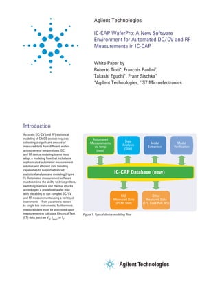
Introduction
Accurate DC/CV (and RF) statistical
modeling of CMOS devices requires
collecting a significant amount of
measured data from different wafers
across several temperatures. DC
and RF device modeling teams must
adopt a modeling flow that includes a
sophisticated automated measurement
solution and efficient data handling
capabilities to support advanced
statistical analysis and modeling (Figure
1). Automated measurement software
must combine the ability to drive probers,
switching matrixes and thermal chucks
according to a predefined wafer map,
with the ability to run complex DC/CV
and RF measurements using a variety of
instruments—from parametric testers
to single box instruments. Furthermore,
measured data must be processed upon
measurement to calculate Electrical Test
(ET) data, such as Vth
, Idmax
, or fT
.
Figure 1. Typical device modeling flow
2. 2
Background
Modern software prober solutions can handle prober positioning, alignment and tempera-
ture control very efficiently, but lack the flexibility to support a customizable measure-
ment library and complex post process data calculation and analysis.
Agilent Technologies is introducing a new turn-key DC/CV and RF automated
characterization solution to help modeling and device engineers achieve more
efficient on-wafer measurements across temperature. This breakthrough solution
is based on the Integrated Circuit Characterization and Analysis Program (IC-CAP)
modeling software and efficiently controls DC/CV analyzers, network analyzers,
probers, switching matrixes, and temperature chucks, as well as the powerful
407x and 408x Series of Agilent parametric testers. The newly designed solution
is called IC-CAP Wafer Professional (IC-CAP WaferPro).
IC-CAP WaferPro is integrated into the IC-CAP platform and takes advantage of its
powerful measurement and programming environment to enable a custom library of
efficient measurement routines (e.g., adaptive measurement algorithms) that can greatly
reduce the overall measurement time. Since the measurement routines are in the IC-CAP
environment, either simple or complex post processing (such as calculation of spot
measurements or figures of merit, RF deembedding and direct extraction), can be applied
to measured data before data is saved. This paper shows a preview of the capabilities
provided by this innovative solution that will be released with IC-CAP 2010.08.
Figure 2: The WaferPro Project Window (wafer map definition)
3. 3
Measurements for device modeling are generally more accurate, extensive and
therefore more time consuming than production-like measurements. Where it may be
sufficient for production tests to probe process control monitors and do single point spot
measurements, in order to characterize how the device model varies versus temperature,
both swept and spot measurement tests must be done for several temperatures (typically
3). For a typical MOS process, acquiring data across a wafer lot at each temperature
requires measuring several geometries, capacitance and diode structures, and may
take several hours. The wafer/prober re-alignment after a change of temperature is
particularly challenging due to wafer thermal expansion in all directions (including z).
Unless sophisticated algorithms using pattern recognition technology can be applied to
automate the proper re-alignment, manual intervention is usually required to re-align the
prober at each temperature.
With measurement taking several hours, or even days, it is important to be as efficient
as possible, without compromising measurement accuracy. Measurement control
software must work in conjunction with the prober native control software, as well as
each instrument, to allow automated measurements across temperature. To maximize
efficiency and avoid measuring bad devices or die, the software should also be able to
run check tests verifying device and die integrity, and then based on the test results,
decide whether to continue, skip the current device or die, or stop the measurement
completely. Additionally, it is important to have the ability to monitor results during test
plan execution, to spot any failure conditions that are reported.
Since this extensive collection of data is then analyzed to statistically identify the
“typical” set of devices that will be used for modeling extraction, it is necessary to
efficiently manage and analyze large quantities of data.
Device Modeling Measurement Challenges
4. 4
IC-CAP WaferPro Benefits
The W8510 IC-CAP WaferPro was designed in partnership with the device modeling
team at ST Microelectronics and represents a solution to real characterization needs.
WaferPro runs on the IC-CAP platform as add-on product. The newly designed WaferPro
project window, as shown in Figure 2, lets users define and manage the test plan which
includes wafer map and device information. WaferPro links to the core IC-CAP program
and utilizes built-in IC-CAP measurement drivers, as well as its simulation, programming
and graphics engines.
IC-CAP WaferPro runs fully automated measurements on semi- and fully automated
probers, and includes drivers for several popular probers.
As previously mentioned, parametric testers such as the Agilent 407x Series coupled
with automatic prober re-alignment supported by major prober vendors are key to
efficient automated measurements across temperature. IC-CAP WaferPro provides the
ultimate flexibility to support direct control of Agilent parametric testers, as well as
simpler single instrument bench setups (e.g., B1500A + B2200A). Unlike other software,
which may be limited to a specific test station or type of prober, once the WaferPro test
plan or project file is defined, the program can drive different test stations composed of
different DC and RF instruments. This allows engineers to optimize lab equipment usage.
IC-CAP WaferPro is a turn-key solution that includes a variety of DC/CV and RF
measurement routines built into the IC-CAP environment. Thanks to IC-CAP’s open and
powerful environment, it is easy to add custom routines or user-defined calculations of
figures of merit (e.g., Vth
for MOS DC or fT
for RF measurements).
While executing the test plan, IC-CAP WaferPro conveniently saves calculated values
or spot measurements to .csv files along with device information (Figure 3). Swept
measurement data, such as I-V, CV or S-parameter curves, are saved to IC-CAP MDM
data. Furthermore, WaferPro can be used to monitor the actual measurement, to analyze
and verify the so far obtained measurement results, while it continues measuring.
Measured data can be loaded back into the WaferPro environment for further post-
processing (e.g., applying capacitance calibration, etc.).
WaferPro will also be IC-CAP Database enabled. When the new IC-CAP Database link
is available, it will allow saving measured data directly to a specified SQL relational
database. This represents a powerful and versatile data handling solution for further
post-processing and statistical analysis, as it enables the efficient data query necessary
for data analysis and other modeling activities (e.g., target modeling).
Figure 3: WaferPro Device Info Table (probe card view)
5. 5
How IC-CAP WaferPro Works
The new measurement environment includes two IC-CAP model files (Routine and Driver)
and the new WaferPro test plan manager (Figure 4). The Routine model includes the
routine measurement library; each routine is represented by one DUT and its setups.
The Driver model file includes the drivers for supported probers, switching matrixes and
thermal chucks.
Figure 4: WaferPro communicates with IC-CAP through an internal link
The second part of the WaferPro solution is the new WaferPro Project Window. This
window environment manages the wafer map information (Figure 2), the device tables
(Figure 3), and the test plan definition and execution (Figure 5).
A test plan is defined by first specifying the wafer, dies and subsites. The second step is
to build lists of “target devices” by selecting devices that are suitable to be measured by
the same routine algorithm (e.g., DC devices, capacitance structures, open devices, etc.).
Lot
Wafers
Dies
Blocks
Subsite
Devices Characterization
Step
Target
Device
Lists
Technology Space
Target Die
Lists
Measurement
Definition
Bench
or test station
Routines
DC, C-V, Spot etc.
Measurement Conditions
Database
or File
Test Plan Sequence: Wafer, Dies List,
Temp, Characterization Steps
Figure 5: The WaferPro wafer map and test plan definition nomenclature
6. 6
The next step is building the “characterization steps” by associating a routine and
its measurement conditions (e.g., bias information, integration time, etc.) to each
target device list. The final step is specifying the test plan to define the sequence of
characterization steps applied to specified wafers, die lists and temperature.
When the test plan is run, a second IC-CAP process is launched, to execute the test
plan as a background process. At any time during the execution, the user can monitor a
comprehensive log that shows the current test plan status and each single test result,
including any failures, or warning conditions and related comments (Figure 6). It is also
possible to view the results of a particular test by simply selecting the specific test and
opening the related multiplot display.
Figure 6: Test plan run page and its log information with display capabilities. The display also shows the DUT
information, as well as all the calculated data (or spot data) included in this routine.