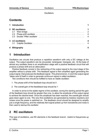
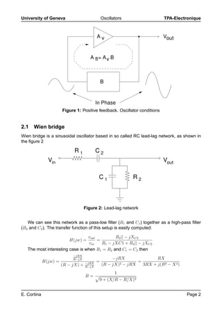
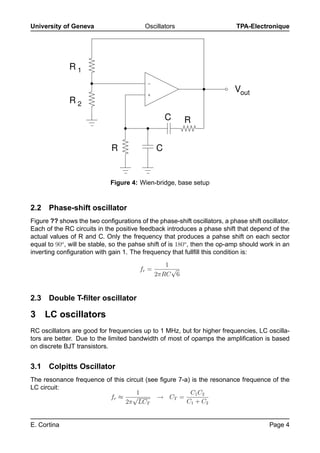
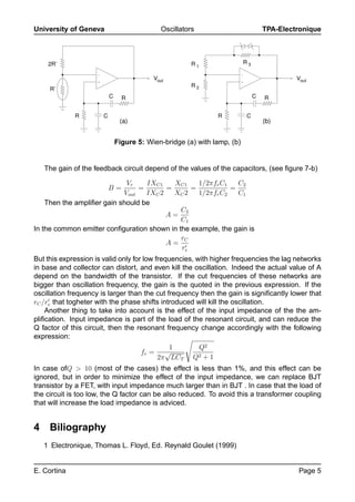
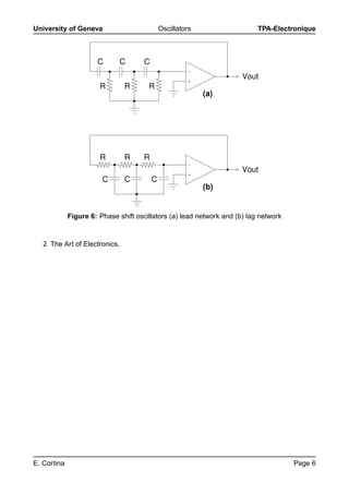
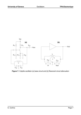
University of Geneva                       Oscillators                        TPA-Electronique

                                           Oscillators


Contents
1 Introduction                                                                                  1

2 RC oscillators                                                                                1
  2.1 Wien bridge . . . . . . . . . . . . . . . . . . . . . . . . . . . . . . . . . . . . .     2
  2.2 Phase-shift oscillator . . . . . . . . . . . . . . . . . . . . . . . . . . . . . . . .    4
  2.3 Double T-filter oscillator . . . . . . . . . . . . . . . . . . . . . . . . . . . . . .     4

3 LC oscillators                                                                                4
  3.1 Colpitts Oscillator . . . . . . . . . . . . . . . . . . . . . . . . . . . . . . . . . .   4

4 Biliography                                                                                   5


1     Introduction
Oscillators are circuits that produce a repetitive waveform with only a DC voltage at the
output. The output waveform can be sinusoidal, rectangular, triangular, etc. At the base of
almost any oscillator there is an amplification stage with a positive feedback circuit that will
produce a phase shift and an attenuation.
    Positive feedback consist in the redirecting of the output signal to the input stage of the
amplifier without a phase shift. This feedback signal is then amplified again generating the
output signal, that produces the feedback signal. This phenomenon, in wich the output signal
“takes care”of itself in order to generate continuum signal is called oscillation.
    Two conditions then should be fulfilled to have an stable oscillator:

    1. The phase shift of the feedback loop should be 0

    2. The overall gain of the feeddback loop should be 1

    In order to arrive to the stable regime of the oscillator, during the starting period the gain
of the feedback loop should be greater than one, to allow the amplitude of the output signal
to achieve the desired level. Once this amplitude has been reached, the overall gain should
goes down again to one. The very first oscillations are generated by trasitory reactions and
noises once the power is switched on. The feedback circuit should be designed to amplify
just a single frequency, and the relatively faint signal picked up from transitories and noise is
then used to startup the oscillator


2     RC oscillators
This type of oscillators, use RC elements in the feedback branch. Useful to frequencies up
to 1 MHz.


E. Cortina                                                                                 Page 1
University of Geneva                           Oscillators                  TPA-Electronique


                                           Av                               Vout


                                       A fl = A v B


                                               B


                                           In Phase
                       Figure 1: Positive feedback. Oscillator conditions


2.1   Wien bridge
Wien bridge is a sinusoidal oscillator based in so called RC lead-lag network, as shown in
the figure 2

                             R1            C2
               Vin                                                          Vout

                                            C1               R2


                                    Figure 2: Lead-lag network


   We can see this network as a pass-low filter (R1 and C1 ) together as a high-pass filter
(R2 and C2 ). The transfer function of this setup is easily computed:

                                 vout         R2 || − jXC2
                          H(jw) =     =
                                  vin   R1 − jXC1 + R2 || − jXC2
   The most interesting case is when R1 = R2 and C1 = C2 then
                            −jRX
                            R−jX                    −jRX               RX
             H(jw) =                −jRX
                                           =           2 − jRX
                                                               =
                       (R − jX) +   R−jX
                                               (R − jX)          3RX + j(R2 − X 2 )
                                                      1
                                    B=
                                            9 + (X/R − R/X)2


E. Cortina                                                                            Page 2
University of Geneva                                      Oscillators                                                 TPA-Electronique

                                            X/R − R/X
                                                φ = arctan
                                                  3
   In figure 3 are shown both the gain in tension (B) as the phase shift (φ) as a function of
the frequency. The oscillating frequency is
                                                                          1
                                                        fr =
                                                                        2πRC
and for this frequency we have that B = 1/3 and φ = 0o . This means that the amplifier
should have a gain A = 3 and introduce a phase shift φ = 0o /
                             Gain                                        Phase shift


                                                                         80
                              0.3
                                                                         60

                             0.25                                        40

                                                                         20
                              0.2
                                                                          0
                             0.15
                                                                         -20

                              0.1                                        -40

                                                                         -60
                             0.05
                                                                         -80
                               0 -2        -1                                  -2           -1
                               10     10          1     10                10           10        1     10
                                                      Frequency (au)                                 Frequency (au)


             Figure 3: Lead-lag network gain and phase shift for RC = 1/2π


   In the figure 4 is shown the base schematics of a Wien oscillator, based in an opamp.
The positive feedback is created by the lead-jag network, and the negative feedback create
a non-inverting amplifer with gain
                                                      R1
                                    A=1+                 =3                    → R1 = 2R2
                                                      R2
   In the beginning, the gain of the negative feedback should be greater than 3, and later,
once the output amplitude has been achieved, go back to 3. There are various methods to
accomplish it in an automatic way.

  1. The most easy and classical method is to use a low power incandescende lamp instead
     of R2 . When swicth on, the resistance of the lamp is small, giving an amplification
     greater that 3. Once the oscillations grows in amplitude the resistance also goes up,
     arriving to a value R in the desired amplitude. If the feedback resistance is chosen to
     be R1 = 2R , we will obtain automatically a gain A = 3, giving the stable oscillations.
     See figure 5

  2. Another method consist is adding a third resistor R3 in parallel with two zener diodes
     conected back to back as shown in figure ??. When switch on, the zener diodes are in
     open circuit, giving then the value of the gain as:
                                                                       R1 + R3     R3
                                                 A=1+                          =3+
                                                                         R2        R2
     Once the output arrives to the zener voltage, the diodes short circuit the resistor restor-
     ing the gain A = 3 and the output signal becomes stable.


E. Cortina                                                                                                                     Page 3
University of Geneva                      Oscillators                       TPA-Electronique


              R1
                                           −

                                           +
                                                                           Vout
              R2
                                                   C     R


                             R                 C


                             Figure 4: Wien-bridge, base setup


2.2   Phase-shift oscillator
Figure ?? shows the two configurations of the phase-shift oscillators, a phase shift oscillator.
Each of the RC circuits in the positive feedback introduces a phase shift that depend of the
actual values of R and C. Only the frequency that produces a pahse shift on each sector
equal to 90o , will be stable, so the pahse shift of is 180o , then the op-amp should work in an
inverting configuration with gain 1. The frequency that fullfill this condition is:
                                                  1
                                        fr =        √
                                               2πRC 6


2.3   Double T-filter oscillator

3     LC oscillators
RC oscillators are good for frequencies up to 1 MHz, but for higher frequencies, LC oscilla-
tors are better. Due to the limited bandwidth of most of opamps the amplification is based
on discrete BJT transistors.


3.1   Colpitts Oscillator
The resonance frequence of this circuit (see figure 7-a) is the resonance frequence of the
LC circuit:
                                    1                  C1 C2
                         fr ≈ √             → CT =
                                2π LCT                C1 + C2


E. Cortina                                                                              Page 4
University of Geneva                            Oscillators                              TPA-Electronique


     2R’                                                  R1                    R3

                     −                                                      −

                     +
                                             Vout                           +
                                                                                                  Vout
                                                          R2
     R’
                             C     R                                                 C   R


             R           C                                         R            C
                                  (a)                                                    (b)


                                 Figure 5: Wien-bridge (a) with lamp, (b)


    The gain of the feedback circuit depend of the values of the capacitors, (see figure 7-b)

                             Vr    IXC1    XC1    1/2πfr C1   C2
                             B=  =       =      =           =
                            Vout   IXC 2   XC 2   1/2πfr C2   C1
    Then the amplifier gain should be
                                             C2
                                         A=
                                             C1
In the common emitter configuration shown in the example, the gain is
                                             rC
                                         A=
                                             re
But this expression is valid only for low frequencies, with higher frequencies the lag networks
in base and collector can distort, and even kill the oscillation. Indeed the actual value of A
depend on the bandwidth of the transistor. If the cut frequencies of these networks are
bigger than oscillation frequency, the gain is the quoted in the previous expression. If the
oscillation frequency is larger than the cut frequency then the gain is significantly lower that
rC /re that togheter with the phase shifts introduced will kill the oscillation.
    Another thing to take into account is the effect of the input impedance of the the am-
plification. Input impedance is part of the load of the resonant circuit, and can reduce the
Q factor of this circuit, then the resonant frequency change accordingly with the following
expression:
                                                   1       Q2
                                         fr =     √
                                                2π LCT    Q2 + 1
In case ofQ > 10 (most of the cases) the effect is less than 1%, and this effect can be
ignored, but in order to minimize the effect of the input impedance, we can replace BJT
transistor by a FET, with input impedance much larger than in BJT . In case that the load of
the circuit is too low, the Q factor can be also reduced. To avoid this a transformer coupling
that will increase the load impedance is adviced.


4    Biliography
    1 Electronique, Thomas L. Floyd, Ed. Reynald Goulet (1999)


E. Cortina                                                                                        Page 5
University of Geneva                          Oscillators                  TPA-Electronique


                      C        C      C
                                                        −

                                                        +
                                                                      Vout
                       R       R       R
                                                            (a)


                       R       R      R
                                                        −

                                                        +
                                                                      Vout
                        C      C          C
                                                            (b)


             Figure 6: Phase shift oscillators (a) lead network and (b) lag network


   2 The Art of Electronics,


E. Cortina                                                                            Page 6
University of Geneva                           Oscillators                    TPA-Electronique


                  Vcc

                             (a)                                        (b)
       R1               R1         C2
                                                                                      Vout
                                        Vout


                                                                  L
       R1     R1             C2


                                                                  I
                                                             C2       C2
              L
                                                             Vr       Vout
         C2        C2

     Figure 7: Colpitts oscillator (a) base circuit and (b) Resonant circuit attenuation


E. Cortina                                                                             Page 7

oscillators

  • 1.
    University of Geneva Oscillators TPA-Electronique Oscillators Contents 1 Introduction 1 2 RC oscillators 1 2.1 Wien bridge . . . . . . . . . . . . . . . . . . . . . . . . . . . . . . . . . . . . . 2 2.2 Phase-shift oscillator . . . . . . . . . . . . . . . . . . . . . . . . . . . . . . . . 4 2.3 Double T-filter oscillator . . . . . . . . . . . . . . . . . . . . . . . . . . . . . . 4 3 LC oscillators 4 3.1 Colpitts Oscillator . . . . . . . . . . . . . . . . . . . . . . . . . . . . . . . . . . 4 4 Biliography 5 1 Introduction Oscillators are circuits that produce a repetitive waveform with only a DC voltage at the output. The output waveform can be sinusoidal, rectangular, triangular, etc. At the base of almost any oscillator there is an amplification stage with a positive feedback circuit that will produce a phase shift and an attenuation. Positive feedback consist in the redirecting of the output signal to the input stage of the amplifier without a phase shift. This feedback signal is then amplified again generating the output signal, that produces the feedback signal. This phenomenon, in wich the output signal “takes care”of itself in order to generate continuum signal is called oscillation. Two conditions then should be fulfilled to have an stable oscillator: 1. The phase shift of the feedback loop should be 0 2. The overall gain of the feeddback loop should be 1 In order to arrive to the stable regime of the oscillator, during the starting period the gain of the feedback loop should be greater than one, to allow the amplitude of the output signal to achieve the desired level. Once this amplitude has been reached, the overall gain should goes down again to one. The very first oscillations are generated by trasitory reactions and noises once the power is switched on. The feedback circuit should be designed to amplify just a single frequency, and the relatively faint signal picked up from transitories and noise is then used to startup the oscillator 2 RC oscillators This type of oscillators, use RC elements in the feedback branch. Useful to frequencies up to 1 MHz. E. Cortina Page 1
  • 2.
    University of Geneva Oscillators TPA-Electronique Av Vout A fl = A v B B In Phase Figure 1: Positive feedback. Oscillator conditions 2.1 Wien bridge Wien bridge is a sinusoidal oscillator based in so called RC lead-lag network, as shown in the figure 2 R1 C2 Vin Vout C1 R2 Figure 2: Lead-lag network We can see this network as a pass-low filter (R1 and C1 ) together as a high-pass filter (R2 and C2 ). The transfer function of this setup is easily computed: vout R2 || − jXC2 H(jw) = = vin R1 − jXC1 + R2 || − jXC2 The most interesting case is when R1 = R2 and C1 = C2 then −jRX R−jX −jRX RX H(jw) = −jRX = 2 − jRX = (R − jX) + R−jX (R − jX) 3RX + j(R2 − X 2 ) 1 B= 9 + (X/R − R/X)2 E. Cortina Page 2
  • 3.
    University of Geneva Oscillators TPA-Electronique X/R − R/X φ = arctan 3 In figure 3 are shown both the gain in tension (B) as the phase shift (φ) as a function of the frequency. The oscillating frequency is 1 fr = 2πRC and for this frequency we have that B = 1/3 and φ = 0o . This means that the amplifier should have a gain A = 3 and introduce a phase shift φ = 0o / Gain Phase shift 80 0.3 60 0.25 40 20 0.2 0 0.15 -20 0.1 -40 -60 0.05 -80 0 -2 -1 -2 -1 10 10 1 10 10 10 1 10 Frequency (au) Frequency (au) Figure 3: Lead-lag network gain and phase shift for RC = 1/2π In the figure 4 is shown the base schematics of a Wien oscillator, based in an opamp. The positive feedback is created by the lead-jag network, and the negative feedback create a non-inverting amplifer with gain R1 A=1+ =3 → R1 = 2R2 R2 In the beginning, the gain of the negative feedback should be greater than 3, and later, once the output amplitude has been achieved, go back to 3. There are various methods to accomplish it in an automatic way. 1. The most easy and classical method is to use a low power incandescende lamp instead of R2 . When swicth on, the resistance of the lamp is small, giving an amplification greater that 3. Once the oscillations grows in amplitude the resistance also goes up, arriving to a value R in the desired amplitude. If the feedback resistance is chosen to be R1 = 2R , we will obtain automatically a gain A = 3, giving the stable oscillations. See figure 5 2. Another method consist is adding a third resistor R3 in parallel with two zener diodes conected back to back as shown in figure ??. When switch on, the zener diodes are in open circuit, giving then the value of the gain as: R1 + R3 R3 A=1+ =3+ R2 R2 Once the output arrives to the zener voltage, the diodes short circuit the resistor restor- ing the gain A = 3 and the output signal becomes stable. E. Cortina Page 3
  • 4.
    University of Geneva Oscillators TPA-Electronique R1 − + Vout R2 C R R C Figure 4: Wien-bridge, base setup 2.2 Phase-shift oscillator Figure ?? shows the two configurations of the phase-shift oscillators, a phase shift oscillator. Each of the RC circuits in the positive feedback introduces a phase shift that depend of the actual values of R and C. Only the frequency that produces a pahse shift on each sector equal to 90o , will be stable, so the pahse shift of is 180o , then the op-amp should work in an inverting configuration with gain 1. The frequency that fullfill this condition is: 1 fr = √ 2πRC 6 2.3 Double T-filter oscillator 3 LC oscillators RC oscillators are good for frequencies up to 1 MHz, but for higher frequencies, LC oscilla- tors are better. Due to the limited bandwidth of most of opamps the amplification is based on discrete BJT transistors. 3.1 Colpitts Oscillator The resonance frequence of this circuit (see figure 7-a) is the resonance frequence of the LC circuit: 1 C1 C2 fr ≈ √ → CT = 2π LCT C1 + C2 E. Cortina Page 4
  • 5.
    University of Geneva Oscillators TPA-Electronique 2R’ R1 R3 − − + Vout + Vout R2 R’ C R C R R C R C (a) (b) Figure 5: Wien-bridge (a) with lamp, (b) The gain of the feedback circuit depend of the values of the capacitors, (see figure 7-b) Vr IXC1 XC1 1/2πfr C1 C2 B= = = = = Vout IXC 2 XC 2 1/2πfr C2 C1 Then the amplifier gain should be C2 A= C1 In the common emitter configuration shown in the example, the gain is rC A= re But this expression is valid only for low frequencies, with higher frequencies the lag networks in base and collector can distort, and even kill the oscillation. Indeed the actual value of A depend on the bandwidth of the transistor. If the cut frequencies of these networks are bigger than oscillation frequency, the gain is the quoted in the previous expression. If the oscillation frequency is larger than the cut frequency then the gain is significantly lower that rC /re that togheter with the phase shifts introduced will kill the oscillation. Another thing to take into account is the effect of the input impedance of the the am- plification. Input impedance is part of the load of the resonant circuit, and can reduce the Q factor of this circuit, then the resonant frequency change accordingly with the following expression: 1 Q2 fr = √ 2π LCT Q2 + 1 In case ofQ > 10 (most of the cases) the effect is less than 1%, and this effect can be ignored, but in order to minimize the effect of the input impedance, we can replace BJT transistor by a FET, with input impedance much larger than in BJT . In case that the load of the circuit is too low, the Q factor can be also reduced. To avoid this a transformer coupling that will increase the load impedance is adviced. 4 Biliography 1 Electronique, Thomas L. Floyd, Ed. Reynald Goulet (1999) E. Cortina Page 5
  • 6.
    University of Geneva Oscillators TPA-Electronique C C C − + Vout R R R (a) R R R − + Vout C C C (b) Figure 6: Phase shift oscillators (a) lead network and (b) lag network 2 The Art of Electronics, E. Cortina Page 6
  • 7.
    University of Geneva Oscillators TPA-Electronique Vcc (a) (b) R1 R1 C2 Vout Vout L R1 R1 C2 I C2 C2 L Vr Vout C2 C2 Figure 7: Colpitts oscillator (a) base circuit and (b) Resonant circuit attenuation E. Cortina Page 7