Electronics and Communication Engineering
•
0 likes•34 views

Electronics and Communication Engineering is the Branch of Engineering. Electronics and Communication Engineering field requires an understanding of core areas including Engineering Graphics, Computer Programming,Electronics Devices and Circuits-I, Network Analysis, Signals and Systems, Communication Systems, Electromagnetics Engineering, Digital Signal Processing, Embedded Systems, Microprocessor and Computer Architecture. Ekeeda offers Online Mechanical Engineering Courses for all the Subjects as per the Syllabus. Visit : https://ekeeda.com/streamdetails/stream/Electronics-and-Communication-Engineering

Recommended
More Related Content
What's hot
What's hot (19)
Similar to Electronics and Communication Engineering
Similar to Electronics and Communication Engineering (20)
More from Ekeeda
More from Ekeeda (20)
Recently uploaded
Recently uploaded (20)
Electronics and Communication Engineering
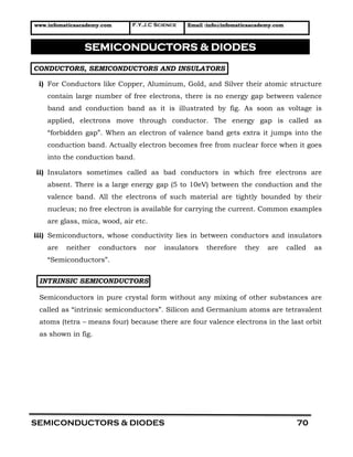
- 1. www.infomaticaacademy.com F.Y.J.C Science Email :info@infomaticaacademy.com SEMICONDUCTORS & DIODES 70 CONDUCTORS, SEMICONDUCTORS AND INSULATORS i) For Conductors like Copper, Aluminum, Gold, and Silver their atomic structure contain large number of free electrons, there is no energy gap between valence band and conduction band as it is illustrated by fig. As soon as voltage is applied, electrons move through conductor. The energy gap is called as “forbidden gap”. When an electron of valence band gets extra it jumps into the conduction band. Actually electron becomes free from nuclear force when it goes into the conduction band. ii) Insulators sometimes called as bad conductors in which free electrons are absent. There is a large energy gap (5 to 10eV) between the conduction and the valence band. All the electrons of such material are tightly bounded by their nucleus; no free electron is available for carrying the current. Common examples are glass, mica, wood, air etc. iii) Semiconductors, whose conductivity lies in between conductors and insulators are neither conductors nor insulators therefore they are called as “Semiconductors”. INTRINSIC SEMICONDUCTORS Semiconductors in pure crystal form without any mixing of other substances are called as “intrinsic semiconductors”. Silicon and Germanium atoms are tetravalent atoms (tetra – means four) because there are four valence electrons in the last orbit as shown in fig. SEMICONDUCTORS & DIODES
- 2. www.infomaticaacademy.com F.Y.J.C Science Email :info@infomaticaacademy.com SEMICONDUCTORS & DIODES 71 Fig. shows an intrinsic semiconductor crystal structures. Each valence electron forms a covalent bond with adjacent atom. That means all valence electrons form covalent bonds, no electron is therefore free for carrying the current thus at absolute zero temperature, semiconductor is an insulator. When extra energy is supplied to this crystal either by applying voltage or applying light these electrons become free from covalent bond, they may go into the conduction band from valence band. The energy required to break covalent bond is 1.12 Volt for Silicon and 0.75 eVolt for Germanium. When electron jumps into the conduction band it leaves an empty space called as a „hole‟. The formation of electron hole pair is simultaneous. The number of electrons and holes are equal such generation of electron hole pair is called „thermal generation‟. EXTRINSIC SEMICONDUTORS Most of the active components are manufactured by using extrinsic – N – type and P-type semiconductors. When other atoms or impurity either trivalent or pentavalent is added to intrinsic semiconductor to increase either number of electrons or holes such type of semiconductor is called as „extrinsic‟ semiconductor. The process of adding such impurity to a pure crystal of semiconductor is called as „doping‟. A doped semiconductor is an extrinsic semiconductor. The two types of semiconductors can be formed
- 3. www.infomaticaacademy.com F.Y.J.C Science Email :info@infomaticaacademy.com SEMICONDUCTORS & DIODES 72 (i) N-type Semiconductor (ii) P-type Semiconductor (i) N-type Semiconductor A semiconductor with majority electrons is called as N-type semiconductor (N-Negative electrons). N-type Semiconductor is formed by adding pentavalent atoms to an intrinsic semiconductor. The doping atoms are Arsenic (As), Antimony (Sb) or Phosphorus (P); they have 5 valence electrons, each pentavalent atom has 5 electrons in the outermost orbit. Now 4 of them will form covalent bonds with Silicon or Germanium atom therefore one extra electron becomes free electrons as shown in fig (1.3). Since this electron is far away from the nucleus and it is free from covalent bond, it is available as conduction band electron for carrying the current. Thus in N-type semiconductor we get more electrons in addition to thermally generated electron-hole pairs. Here the pentavalent atom is known as „donor‟ atom because it donates electron to Silicon or Germanium. In N-type semiconductor electrons are called as majority charge carries and holes are minority charge carriers.
- 4. www.infomaticaacademy.com F.Y.J.C Science Email :info@infomaticaacademy.com SEMICONDUCTORS & DIODES 73 A Semiconductor with excess number of holes (holes –positive- „P‟) is called as P-type semiconductor. Trivalent (Tri-three valence electrons) atoms are added to a pure crystal of semiconductor to form this semiconductor. Trivalent impurity as Aluminum (Al), Boron (B), Gallium (Ga) or Indium (In) are used as „acceptors‟. Since each trivalent atom has three valence electrons, they will form covalent bond with silicon atom but the fourth Silicon atom unable to form covalent bond with Boron atom, because Boron do not have fourth valence electron. Thus an empty space called as hole is created because of trivalent atom as shown in fig (1.3b). Doping with a number of trivalent atoms P-type semiconductor is formed where more holes are available for carrying the current. This hole can accept one electron therefore trivalent impurity is called as „acceptors‟. Thermally generated electron – holes are there, so electrons are few called as „minority‟ carriers and holes are called as „majority‟ carriers. COMPARISON N-type Semiconductor P-type Semiconductor 1) Doped with Pentavalent atoms. 1) Doped with trivalent atoms. 2)Electrons are majority charge carriers. 2) Holes are majority charge carriers. 3)Holes are minority carriers. 3) Electrons are minority carriers. 4) Pentavalent atoms give electron therefore called as donor atoms 4) Trivalent atoms create hole, therefore called as acceptor atoms. 5) Antimony, Arsenic, Phosphorus impurity is required 5) Aluminum, Boron, Indium, Gallium impurity is required
- 5. www.infomaticaacademy.com F.Y.J.C Science Email :info@infomaticaacademy.com SEMICONDUCTORS & DIODES 74 P-N JUNCTION DIODE Semiconductor diode is similar to a valve diode; P-type semiconductor is joined with N-type semiconductor so it forms a P-N junction diode. P-type material is acting as anode and N type as cathode. Fig. shows this structure and symbol of P-N diode. Barrier Potential As soon as junction is formed some of the electrons from N-region near the junction cross the junction and fill some of the holes of P-region as shown in above fig. Since the atoms of N-region loose electrons they become positively charged ions and since the atoms of P-regions accept electrons they become positively charged ions and since the atoms of P-region accept electrons they become negatively charged ions. Thus opposite types of ions are produced (Positive ions on N-side and negative ions on P-side) near the junction as shown in above fig. These ions oppose further flow of electrons from N to P region and flow of holes from P to N region. The opposing force of ions is called as barrier potential and this region is called as „depletion region‟. This barrier potential is a 0.7V in case of silicon diode and 0.3V in case of Germanium diode. Forward Bias Bias means to apply voltage across P-N junction. In Forward bias, anode is connected to positive terminal and cathode to negative terminal of the battery. Fig. shows forward bias connections and it shows maximum current through the
- 6. www.infomaticaacademy.com F.Y.J.C Science Email :info@infomaticaacademy.com SEMICONDUCTORS & DIODES 75 diode. In forward bias the resistance of diode becomes very low. Diode is acting as a close switch. Let us see how current flows through P-N junction. The negative terminal of the battery will repel electrons at N-region those move towards the junction as shown in fig. and they overcome potential barrier because battery voltage is more than 0.7V or 0.3V for Silicon and Germanium respectively. They electrons move through P-region to the left side of the junction and then collected by the positive terminal. Similarly because of this holes are attracted by the negative terminal and flows in opposite direction. Reverse Bias This is another way of connecting a diode, P-region (anode) to negative terminal and N-region (Cathode) to positive terminal of the battery, and it is called as „reverse bias‟. In this condition since reverse battery voltage is applied across the junction the width of potential barrier increases. This barrier will not allow the movement of majority carriers from N to P region. The current through
- 7. www.infomaticaacademy.com F.Y.J.C Science Email :info@infomaticaacademy.com SEMICONDUCTORS & DIODES 76 diode is not possible which indicates a very high resistance or diode is acting as an open switch as shown in the fig. Practically, very small current flows through diode, which is called as „reverse leakage current‟ because of minority carries. P-region has few minority electrons (generated by thermal electron-hole pairs) those are repelled by negative terminal and they flow through the junction towards right side through N – region and then towards positive terminal of the battery. a) Forward Characteristics When P-N junction diode is connected in forward bias its N-region has free electrons refer fig. (a), in conduction band and P-region has holes in Valence band. P-region has slightly higher energy level. Let us consider single electron movement from –ve terminal to the +ve terminal of the battery. i) It is repelled by negative terminal so it travels through N-region as a free electron in conduction band.
- 8. www.infomaticaacademy.com F.Y.J.C Science Email :info@infomaticaacademy.com SEMICONDUCTORS & DIODES 77 ii) Near the junction it jumps from conduction band it recombines with hole & becomes valence electron in Valence band. iii) Now it is in P-region it travels through P-region as a valence electron and finally it is collected by positive terminal of the battery. b) Reverse Characteristics In reverse bias as explained earlier free electrons in N-region go away from the junction, and holes in P-region move away from the junction. As shown in the fig. the leaving electrons near the junction leave more +ve ions and the leaving holes near the junction leave more –ve ions. It results in wider depletion layer. Refer energy level diagram, in reverse bias conduction band electrons and valence band holes go away from the junction the width of barrier or depletion layer gets wider till it becomes equal to the battery voltage. BLOCK DIAGRAM OF POWER SUPPLY
- 9. www.infomaticaacademy.com F.Y.J.C Science Email :info@infomaticaacademy.com SEMICONDUCTORS & DIODES 78 1. TRANSFORMER The function of transformer is to transfer 230 V AC into required AC voltage. It depends upon load, which is to be connected across power supply. For example, a tape recorder of 12 V is to be connected across it then a step down transformer of 12 V is connected. Another function of transformer is to provide isolation between primary and secondary winding. Due to this separation, power supply becomes shockproof. 2. RECTIFIERS “The process of converting bi-directional AC voltage into unidirectional DC is known as rectification” and the circuit used for this process is known as rectifier. This circuit is also known by common name “Battery eliminator”. Three circuits are commonly used for rectification i) Half wave rectifier ii) Center tap full wave rectifier iii) Bridge full wave rectifier I. HALF WAVER RECTIFIER An AC Voltage consists of two half cycles as shown in the fig. (1.13) upper half cycle is known as positive half cycle and low cycle is known as negative half cycle.
- 10. www.infomaticaacademy.com F.Y.J.C Science Email :info@infomaticaacademy.com SEMICONDUCTORS & DIODES 79 i) In First half cycle or positive half cycle of AC voltage, suppose transformer secondary terminal „A „ is positive with respect to terminal „B‟ refer fig. (a) diode becomes forward biased it is acting as a closed switch. The current flows through the circuit its flow is from terminal A through RL to terminal B as shown in fig (a). Thus same output voltage is developed across RL similar to half cycle of AC input. ii) In the next cycle (negative half cycle) transformer terminal „B‟ is positive with respect to terminal „A‟ now observe the fig. (b) diode becomes reverse biased; diode
- 11. www.infomaticaacademy.com F.Y.J.C Science Email :info@infomaticaacademy.com SEMICONDUCTORS & DIODES 80 is acting as an open switch thus current through circuit is not possible it is blocked by the diode. The output voltage out L LV I R 0 R 0 V is zero refer waveform fig (b) Thus diode will conduct only at positive half cycle and it rectifies negative half cycle hence it is known as half wave rectifier. Peak – Inverse – Voltage (PIV) Peak inverse voltage is an important rating of rectifier, diode should withstand for this voltage when it is in reverse bias. In negative half cycle when terminal „B‟ of transformer is positive it is at cathode of diode, refer fig (1.16) maximum inverse voltage is peak voltage given as „Vp‟. Advantages 1) Only one diode and normal transformer is required 2) Transformer is not essential for high voltage rectifier. 3) The circuit is simple and low cost. 4) PIV is only „Vp‟ Disadvantages 1) Output of half wave rectifier is less because only half cycle appears in the output. 2) There is wastage of negative half cycle. 3) Since ripple frequency is low there are more ripples that generate poor quality DC. Ripple Factor Ripple is unwanted, it is the part of AC in DC output of rectifier. As shown in the waveform output of half wave rectifier is pulsating DC it is not a constant voltage DC this is known as “ripple”.
- 12. www.infomaticaacademy.com F.Y.J.C Science Email :info@infomaticaacademy.com SEMICONDUCTORS & DIODES 81 II. CENTER TAP FULL WAVE RECTIFIER To utilize negative half cycle; one more diode is connected with special type of transformer called as canter tap transformer. In canter tap transformer the middle terminal is tapped so that its upper terminal (A) and low terminal (B) become opposite in phase. e.g. if the terminal A is +ve the terminal B is –ve with respect to canter tap. Working In canter tap rectifier diodes are conducting in alternate cycle so that current through „RL‟ flows in the same direction for both half cycles. i) Suppose in first half cycle terminal A is positive then B is negative with respect to terminal „C‟. Then diode D1 becomes forward biased and D2 reverse biased observe fig (a) current flows from terminal A – D1 – through RL to terminal center tap „C‟ thus output voltage across RL is developed as shown.
- 13. www.infomaticaacademy.com F.Y.J.C Science Email :info@infomaticaacademy.com SEMICONDUCTORS & DIODES 82 ii) In the next half cycle of AC, polarity of AB get reversed A becomes negative and B positive with respect to terminal „C‟. The diode D1 becomes reverse biased and D2 forward biased. Current flows from terminal B through D2 through RL to terminal „C‟ thus output voltage is developed which is Similar to half cycle and it is in the same direction. Fig. Shows input AC and full wave DC output. Advantages of C.T. Rectifier 1) More DC voltage than half wave. 2) Ripple frequency is doubled because two cycles are developed it is 2 fin. If it is 50Hz AC, for full wave rectifier then ripple frequency is 100 Hz, therefore more ripple frequency, it means less ripple than half wave. Ripple factor is 0.48. Disadvantages 1) Center tap transformer is essential which increase the cost. 2) PIV = 2 Vp therefore the cost of diode is more. 3) Still ripple is there, output is full wave pulsating DC. III. BRIDGE FULL WAVE RECTIFIER This is more popular rectifier circuit because the output is full wave DC and center tap transformer is not required. Fig. shows the circuit diagram of Bridge rectifier. Working Refer below figures for both half cycles of AC, current through LR is flowing in the same direction like canter tap rectifier. But in bridge rectifier in each half cycle two diodes are in forward bias and other two diodes are in reverse bias.
- 14. www.infomaticaacademy.com F.Y.J.C Science Email :info@infomaticaacademy.com SEMICONDUCTORS & DIODES 83 i) Suppose in first half cycle of AC, terminal „A „ is positive with respect to terminal „B‟ then diode 1D and 3D become forward biased and 2D , 4D become reverse biased. Now refer fig. current direction is from terminal „A‟ through 1D through LR through 3D to terminal B, thus output voltage is developed across LR L O L LR V =I ×R . ii)Next half cycle, terminal „B‟ is positive with respect to terminal „A‟. Now refer fig. diode 2D , 4D become forward biased and 1D , 3D become reverse biased. Current through circuit is from terminal „B‟ through 2D through LR through 4D to terminal „A‟ that indicates current through LR is in the same direction as in first half cycle.
- 15. www.infomaticaacademy.com F.Y.J.C Science Email :info@infomaticaacademy.com SEMICONDUCTORS & DIODES 84 Advantages 1) More DC output voltage than half wave. 2) Ripple is less because ripple frequency is in2f = 100 Hzand triple factor is 0.48. 3) Center tap transformer is not required that means low cost of transformer. 4) Peak inverse voltage is only PV because maximum secondary voltage of transformer is PV , in bridge rectifier PIV appears across two diodes. Disadvantages 1) In Bridge rectifier, only drawback is 4 diodes are required but it is not much important. 2) Similarly, another drawback in bridge rectifier is for each half cycle two diodes are conducting and both diodes are in series with LR that drops output voltage by (0.7V+0.7V=1.4 volts) where 0.7V drop takes place across diode if it is silicon diode. It reduces the output voltage by 1.4V. It is significant in low voltage power supply. COMPARISON OF RECTIFIERS The points of comparison (Parameters) Half Wave Rectifier C.T. Full Wave Rectifier Bridge Rectifier 1) Number of diodes One Two Four 2) Need of C.T. transfer Not required Essential Not required 3) PIV of diode PV 2 PV PV 4) Average of DC output voltage PV / 2 PV / 2 PV / 5) Ripple frequency Fin (50Hz) 2fin (100Hz) 2fin (100Hz) 6) Current through diode OI = DC LI or I DC LI /2 or I /2 DC LI /2 or I /2 7) Ripple factor 1.21 0.48 0.48
- 16. www.infomaticaacademy.com F.Y.J.C Science Email :info@infomaticaacademy.com SEMICONDUCTORS & DIODES 85 SOLVED PROBLEMS 1) What is the frequency of ripple in output for 50Hz 230V rms line with half wave rectifier and 60Hz 110V rms line input with bridge rectifier? Solution 1. For Half wave rectifier 2. For Bridge rectifier ripple frequency = fin ripple frequency = 2 fin = 50 Hz == 2 60Hz = 120 Hz 2) A transformer has turns ratio 12:1 its primery is connected to 220 V, 50 Hz power line calculate DC output Voltage, PIV of diode and ripple frequency for half wave and Bridge full wave rectifier. Solution Mains Voltage is given as 220 V but it is RMS Voltage. It must be converted in to Peak Voltage. 2rmsPeak primeryvoltage V 220 2 311V Therefore peak secondary voltage can be calculated from turn‟s ratio 1 1 2 2 N V N V 1 2 2 1 311 1 ( ) 12 V N V Peak SecondaryVoltage N Let us say (VP)=25.9 V Peak Secondary Voltage (a) For half wave rectifier 25.9 8.249PV Vdc V [log25.9 log3.14] [1.4133 0.4969] [0.9146] log[0.9146] 8.249Anti Volts PIV = VP = 25.9 V
- 17. www.infomaticaacademy.com F.Y.J.C Science Email :info@infomaticaacademy.com SEMICONDUCTORS & DIODES 86 Ripple frequency = 50 Hz. (b) For Bridge full wave rectifier: 2 2 25.9 16.50PV Vdc V [log2 log25.9 log3.14] [0.3010 1.4133 0.4969] [1.2174] log[1.2174] 16.50Anti V 25.9 ; 2 2 50 100PPIV V V Ripple frequency fin Hz