SlideShare a Scribd company logo
1 of 16
Download to read offline
United States Patent (19)
Himida et al.
(54) BINARY MULTIPLIER CIRCUIT WITH
IMPROVED INPUTS
Hedi Hmida, Paris; Pierre Duhamel,
Issy les Moulineaux, both of France
75 Inventors:
73 Assignee: Etat Francais represente par le
Ministre Delegue des Postes et
Telecommunications (Centre National
d'Etudes des Telecommunications),
Issy les Moulineaux, France
21 Appl. No.: 578,201
22 Filed: Sep. 6, 1990
Related U.S. Application Data
62 Division ofSer. No. 248,089, Sep. 23, 1988.
(30) Foreign Application Priority Data
Sep. 23, 1987 FR France ................................ 87 346
51) Int. Cl............................ G06F 7/52; G06F 7/50
52 U.S.C. ..................................... 364/757; 364/786
58 Field of Search ................ 364/754, 757,784, 786
56) References Cited
U.S. PATENT DOCUMENTS
4,853,887 8/1989 Jutand et al. ........................ 364/757
4,985,862 l/1991 Hnida et al. ....................... 364/786
(fixed B)
Di
||||||||||||I||
USOO5095455A
11 Patent Number:
45 Date of Patent:
5,095,455
Mar. 10, 1992
Primary Examiner-Heather R. Herndon
Assistant Examiner-Long T. Nguyen
Attorney, Agent, or Firm-Foley & Lardner
57 ABSTRACT
Abinary multiplier circuit hasalogic operatoractingas
an exclusive-OR gate generating a first intermediate
signal which is an exclusive-OR of a first input and a
carry-in input. An inverter generates a second interme
diate signal. A second logic operator generates a first
output bit which is a symmetrical exclusive-OR of a
second input and both the first and second intermediate
signals. A second output bit is a symmetrical trigger
function ofthe first and second input, depending on the
firstandsecond intermediatesignals,and is generated in
a transmission gate. Since the carry-in signal passed via
the first and second intermediate signals is applied di
rectlytotransistorsofthetransmission gate, carryprop
agation delay is reduced. A fixed operand is multiplied
by a variable operand by storing a partial result ofthe
multiplication using an accumulator and a shift register
with the binary calculation circuit. A two-input multi
plexerhasoneofitsinputsconnectedto theoutputfrom
the register and an output connected to the input ofthe
register. The variable operand is applied serially to a
control input ofthe multiplexer.
5 Claims, 6 Drawing Sheets
Accumulator
and Shift reqister
5,095,455
Sheet 1 of 6
Mar. 10, 1992
U.S. Patent
wzºu,i----|---------------+---------«-»-,
Sheet 2 of 6 5,095,455
Mar. 10, 1992
U.S. Patent
|
|
|
|
|
|
|
|
|
|
h
S
K
- - - - -
----------
U.S. Patent Mar. 10, 1992 Sheet 3 of 6 5,095,455
---- - - -- - - - -- - - - - - - - - - --------
V
40B 201B
Ri-1S) O3B i)
402B 202B
V3B 2
(Ri-1S)
-l
2
---its-----------------
la)
RS)
U.S. Patent Mar. 10, 1992 Sheet 4 of 6 5,095,455
3C 2.
(RS)
- - - - - - - - - - - - - - - - - - - - - - - - - - - - -
2C
(Ai)
Sheet 5 of 6 5,095,455
Mar. 10, 1992
U.S. Patent
000Z
!
[]
S
U.S. Patent Mar. 10, 1992 Sheet 6 of 6 5,095,455
(fixed B)
Multiplexer
Accumulator
Shift reoister
Di
FIG.8
5,095,455
1.
BINARY MULTIPLER CIRCUIT WITH
IMPROVED INPUTS
This application is a division ofapplication Ser. No.
07/248,089, filed Sept. 23, 1988.
The invention relates to calculations on binary digits,
i.e. bits. It is applicable to realizing binary electronic
systems such asadders, multipliers, dividers, accumula
torS, . . . .
BACKGROUND OF THE INVENTION
The document "Proceedings of the IEEE Interna
tional Conference on Computer Design: VLSI in Com
puters", New York, Oct. 7-10, 1985, pp. 359-362; S.
Steinlechner, and our prior French patent application
number 87 03758 filed Mar. 18, 1987 (and our corre
sponding U.S. patent application Ser. No. 167,787) de
scribe a binary calculation circuit ofthe type compris
ing at least one cell having:
a 1-bitfirstinputfor receivinga firstinputsignal (Ai);
a 1-bit second input for receiving a second input sig
nal (Bi);
a 1-bit carry-in input for receiving a carry-in signal
(Ri-1 S);
first means for generating an exclusive-OR signal
(AiGDBi) and its complement (AieeBi) from the firstand
Second input signals;
second means for producing a result signal by per
formingan exclusive-OR function between the carry-in
signal (Ri-1 S) said exclusive-OR signal (AieBi);
third meansforproducinga carry-out signal (RiS)by
performing a transmission function by means of two
transmission gates controlled by said exclusive-OR sig
nal (AieBi) and its complement (AieeBi), with one of
the gates passing the carry-in signal (Ri-1 S) and the
other gate passing one or other ofthe two input signals
(Ai, Bi).
In the embodiments described in the earlier patent
application, the carry-in signal (Ri-1 S) is applied to the
drainsofthetransistorsequippingthetransmission gates
under the control ofsaid exclusive-OR signal (AieBi)
and its complement (AieBi). This gives riseto a loss of
time during calculation of the carry-out signal (Ri S)
and consequently to a loss ofcarry propagation time in
circuits comprising a plurality ofcells in parallel orga
nized as adder and/or subtracter modules with propa
gated carry.
The Applicants have now observed that by inter
changing the roles of the second input signal (Bi) and
the carry-in signal (Ri-1 S), and by using the intermedi
ate variables thus obtained by said interchange for cal
culating the carry-out signal (RiS), the carry propaga
tion delay in such parallel-connected cells is considera
bly reduced. The carry-in signal (Ri-1 S)passingviathe
exclusive-OR signal (Aieri-1 S) is now applied di
rectly to the grids ofthe transistors in the transmission
gates which are controlled by said exclusive-OR signal
(Aieri-1 S) and its complement (AieeRi-1S).
SUMMARY OF THE INVENTION
More precisely, the present invention provides a bi
nary calculation circuit ofthe type comprising at least
one cell having:
a 1-bitfirstinputfor receivinga firstinput signal (Ai);
a 1-bit second input for receiving a second input sig
nal (Bi); and
5
O
15
20
25
30
35
40
45
50
55
65
2
a 1-bit carry-in input for receiving a carry-in signal
(Ri-1 S);
comprising:
first means for generating an exclusive-OR signal
(AieRi-1 S) between the first input signal and the car
ry-in signal, and the complement thereof(AiGDR-1S),
said complement (AieeRi-1 S) being produced by in
verting the signal (AieeRi-1 S);
second means for producing a result signal by per
forming an exclusive-OR function between the second
inputsignal (Bi) andsaid exclusive-ORsignal (AieRi-1
S) between the first input signal and the carry-in signal;
and
third meansforproducingacarry-outsignal (RiS)by
means ofa transmission function comprising two trans
mission gates controlled by said exclusive-OR signal
(Aieri-1 S) between the first input signal and the car
ry-in signal, and the complement thereof (Aieri-1 S),
with one ofthe gates passing the first input signal (Ai)
and with the other gate passing the second input signal
(Bi).
In a preferred embodiment ofthe invention, the first,
second, and third means are connected in the same
manner as the first, second, and third means respec
tively as claimed in any ofthe claims ofour above-men
tioned earlier patent application, with the 1-bit second
input (Bi) and the 1-bit carry-in input (Ri-1 S) being
interchanged.
The invention also provides a binary calculation cir
cuit of the type comprising at least one basic cell for
adding a first bit (Ai) of arbitrary binary value taken
from a variable operand (A) anda secondbit (Bi) whose
binary value is fixed and known taken from a fixed
operand (B), whereineach cell comprisesafirst module
for delivering an exclusive-OR signal (AieeRi-1 S) be
tween the first input signal and the carry-in signal, and
a second module for producing a carry-out signal (RiS)
by performing a transmission function comprising two
transmission gates under the control of the carry-in
signal (Ri-1 S) and its complement (Ri-1 S), with one of
the gates passing the first input signal (Ai) and with the
other gate passing the second input signal (Bi).
In a preferred embodiment, the binary calculation
circuit according to the invention comprises a plurality
of cells in which the carry-out signal (RiS) from each
cell of rank (i) (0<ian-2) is connected to the 1-bit
carry-in input (RiS) of the cell of rank i-1. Advanta
geously, each cell is hard-wired with the valueofthebit
(Bi) ofthe fixed operand B.
Moreparticularly, thefirst module ofeach cell which
is associated with a bit (Bi) of logic value "0" of the
fixed operand (B) comprisesthree pairs oftransistors as
follows:
a first pair ofopposite polarity transistorscomprising
a first transistor and a second transistor, with the grids
ofboth transistors in the first pair being connected to
receivethe carry-insignal(Ri-1 S),withapositiveelec
tric voltage (V) being applied to the drain of the first
transistor, with ground being applied to the source of
the second transistor, and with the source of the first
transistor and the drain of the second transistor being
interconnected at a first node;
a second pair of opposite polarity transistors, con
prising a first transistorandasecond transistor, with the
drain of the first transistor being connected to receive
the carry-in signal (Ri-1 S), with the source ofthe sec
ond transistor being connected to the first node, with
the gridsofboth transistorsbeingconnected to receive
3
thefirstinputsignal (Ai)from the variable operand (A),
and with the source of the first transistor and the drain
ofthe second transistor being interconnected at a sec
ond node; and
a third pair ofopposite polarity transistors, compris
ing a first transistor and a second transistor, with the
sources of both transistors being connected to the
second node, with the drains of both transistors being
connected to receive thefirst inputsignal (Ai) from the
variable operand (A), with the grid ofthe first transis
tor being connected to receive the carry-in signal
(Ri-1 S), and with the grid of the second transistor
being connected to the first node, such that said exclu
sive-OR signal (AieRi-1 S) between the bits of the
variable operand (A) and the carry-in signal is obtained
at the second node.
According to another aspect of the invention, the
second module of each cell asssociated with a bit (Bi)
oflogic value "O" in the fixed operand (B) comprises:
a fourth pair of opposite polarity transistors, com
prising a first transistor and a second transistor, with
the grid of the first transistor being connected to
receive the carry-in signal (Ri-1 S), with the grid ofthe
second transistor being connected to receive the con
plemented carry-in signal (Ri-1 S), with the drains of
both transistors being connected to receive the first
input signal (Ai) from the variable operand (A), and
with the sources ofboth transistors being connected to
a third node; and
a single third transistor which is an N-channel tran
sistor with itssourceconnected to ground, with its grid
controlled by the complemented carry-in signal Ei
S), and with its drain connected to the third node, the
carry-out signal (RiS) beingobtained at the third node
interconnecting the sources of both transistors in the
fourth pair with the drain ofthe third transistor.
According to another aspect of the invention, the
first module of each cell associated with a bit (Bi) of
logic value "1" of the fixed operand (B) comprises
three pairs oftransistors as follows:
a first pair ofopposite polarity transistors comprising
a first transistor and a second transistor, with the grids
ofboth transistors in the first pair being connected to
receive the carry-in signal (Ri-1 S), with a positive
electric voltage (V) being applied to the drain of the
first transistor, with ground being applied to the source
ofthesecond transistor, and with the source ofthefirst
transistor and the drain of the second transistor being
interconnected at a first node;
a second pair of opposite polarity transistors, com
prising a first transistor and a second transistor, with
the drain of the first transistor being connected to the
first node, with the source of the second transistor
being connected to receive the carry-in signal (Ri-1 S),
with the grids of both transistors being connected to
receive the first input signal (Ai) from the variable
operand (A), and with the soruce ofthe first transistor
and the drain of the second transistor being intercon
nected at a second node; and
a third pair ofopposite polarity transistors, compris
ing a first transistor and a second transistor, with the
sources of both transistors being connected to the
second node, with the drains ofboth transistors being
connected to receivethe first inputsignal (Ai)from the
variable operand (A), with the grid ofthe first transis
torbeingconnected to the first node, and with thegrid
ofthe second transistor being connected to the carry-in
input (Ri-1 S), such that the exclusive-OR signal
(AieeRi-1 S) between the bits ofthe variable operand
5,095,455
5
10
15
20
25
30
35
45
50
55
65
4.
(A) and the carry-in signal is obtained at the second
node.
Accordingto yet another aspectoftheinvention, the
second module ofeach cell associated with a bit (Bi) of
logic value "1" in the fixed operand (B) comprises:
afourth pair ofoppositepolaritytransistors, compris
ing a first transistor and a second transistor, with the
grid ofthefirsttransistorbeingconnected to receivethe
carry-in signal (Ri-1 S), with the grid of the second
transistorbeingconnectedto receivethe complemented
carry-in signal (Ri-1 S), with the drains ofboth transis
tors being connected to receive the first input signal
(Ai) from the variable operand (A), and with the
sources of both transistors being connected to a third
node; and
a single third transistor which is a P-channel transis
tor with itssource connected to a positive electric volt
age (V), with its grid controlled by the complemented
carry-in signal (Ri-1 S), and with its drain connected to
the third node, the carry-out signal (Ri S) being ob
tained at the third node interconnecting the sources of
both transistors in the fourth pair with the drain ofthe
third transistor.
The invention may also be applied to aparallel-series
binary multiplier for multiplying a fixed operand B
comprising nbits Bn-1, Bn-2,..., B0bya variable n-bit
operand D ofarbitrary value having bits Dn-1, Dn-2, .
. . , D0, said multiplier including an accumulator and
shift registerforstoringapartial result ofthemultiplica
tion, said register including an input and an output.
A particular multiplier of this type is described in
French patent application number 86 13222.
According to another characteristic of the present
invention, the multiplier further includes:
a binarycalculation circuitasdescribedaboveinclud
ing and output and an input connected to the output of
the register, each cell ofsaid binary calculation circuit
including a first module for delivering an exclusive-OR
signal (DieRi-1 S) and a second module for producing
a carry-out signal (RiS); and a two-input multiplexer
having one of its inputs connected to the output from
the binary calculation circuit and having its other input
connected to the output from the register, and having
an output connected to the input of the register, said
multiplexer also including a control input to which the
variable operand D is applied in serial form.
In a variant embodiment, forthe purposeofmultiply
ing two opposite-sign operands, the multiplier further
includes a second multiplexer disposed between the
output from the accumulator and shift register and the
input to the adder, said second multiplexer having two
inputs, one connected to the output from the register
and the other connected to the output of an inverter
whose input is connected to the output from the regis
ter, said second multiplexer being controlled by the
most significant bit Dn-1 ofthe operand D.
BRIEF DESCRIPTION OF THE DRAWINGS
Embodiments ofthe invention are described by way
ofexample with reference to theaccompanying draw
ings, in which:
FIG. 1 isacircuitdiagram oftheessential component
parts ofa full adder in accordance with the invention
having three 1-bit inputs (Ai, Bi, and Ri-1 S) andcom
prising 16 transistors;
FIG.2isacircuitdiagramoftheessentialcomponent
parts ofa full adder in accordance with the invention
5,095,455
5
having three 1-bit inputs (Ai, Bi, and Ri-S) and com
prising 15 transistors;
FIG. 3 is a circuit diagram of two modules of an
addition cell in accordance with the invention for add
ing a bit (Ai) ofarbitrary binary value to a bit oflogic
value "0";
FIG. 4 is a circuit diagram of two modules of an
addition cell in accordance with the invention for add
ing a bit (Ai) ofarbitrary binary value to a bit oflogic
value "1":
FIG. 5 is a diagram ofa circuit in accordance with
the invention capable of being configures as either of
the cells described with reference to FIGS. 3 and 4,
with its inputs being programmable as a function ofthe
fixed operand B;
FIG. 6 is a block diagram ofan adder in accordance
with the invention in which the addition cells are hard
wired with the values ofthe bits ofthe fixed operand;
FIG. 7 is a diagram ofthe structure ofa multiplier in
accordancewith theinvention,said multiplierincluding
an adder in accordance with FIG. 6; and
FIG. 8 showsa variant embodiment ofthe multiplier
in accordance with the invention, for processing two
operands of arbitrary sign.
In numerous respects, the accompanying drawings
include information which is definitive in nature. Con
sequently, they may be used not only for facilitating
understanding ofthefollowingdetailed description, but
also for contributing to the definition of the invention,
where appropriate.
MORE DETAILED DESCRIPTION
In FIG. 1, reference 2A designates a full adder in
accordance with the invention having three 1-bit inputs
and comprising 16 transistors.
The addition cell 2A shown in FIG. 1 is practically
identical to the addition cell 2 shown in FIG. 2 of our
above-mentioned prior patent application. It differs
solely in that the second 1-bit input (Bi) has been inter
changed with the 1-bit carry-in input (Ri-1 S), and in
that the letter A has been added to the references ofthe
essential component parts of adder 2A in accordance
with the present invention.
The adder 2A includes a 1-bit first input (Ai), a 1-bit
second input (Bi), and a 1-bit carry-in input (Ri-1 S).
The adder 2A produces a 1-bit result signal (Si). The
result is the sum ofthe two bits (Ai, Bi) and the carry-in
bit (Ri-1 S). It is obtained by calculating the modulo
sun, also known as the exclusive-OR sum, of the first
bit (Ai), the second bit (Bi),and the carry-in bit (Ri-1 S).
Theadder 2A produces a 1-bit carry-outsignal (RiS)
which is associated with the result of calculating the
sum (Si) ofthe three input signals (Ai, Bi, and Ri-1 S).
The carry-out signal (RiS) is obtained by calculating
the sum of the product ofthe two input bits; the prod
uct ofoneoftheinputbits (Ai) and the carry-inbit (Ri-1
S), and the product of the other input bit (Bi) and the
carry-in bit (Ri-1 S).
In order to obtain these two signals, the adder 2A
comprisesfirst means 100A forgeneratingan exclusive
OR signal (AieRi-1 S) between a first one ofthe input
signals (Ai) and the carry-in signal. These first means
100A comprise a pair ofcomplementary MOS technol
ogy transistors 101A and 102A. Transistor 101A is a
P-channel device and transistor 102A is an N-channel
device. Thegrids ofboth transistors 101Aand 102A are
connected to the firstbit input (Ai). An electric voltage
V is applied to the drain D of transistor 101A. For
O
15
25
35
45
50
55
6
example, when the transistors are MOS technology
devices, the value ofV may be 5 volts. Ground is con
nected to the source S oftransistor 102A. The source of
transistor 101A and the drain of transistor 102A are
interconnected at a node 103A. The first means 100A
alsoincludeasecond pair ofcomplementaryMOStech
nology transistors 104A and 105A. Transistor 104A is
P-channel and transistor 105A is N-channel. The drain
oftransistor 104is connected to the 1-bit first input (Ai)
and the source of transistor 105A is connected to the
node 103A. The grids ofthe transistors 104A and 105A
are connected to the 1-bit carry-in input (Ri-1 S). The
source of transistor 104A and the drain of transistor
105A are interconnected at a node 106A.
The first means 100A further include a third pair of
complementary transistors 107A and 108A. Transistor
107A is P-channel and transistor 108A is N-channel.
The sources of transistors 107A and 108A are con
nected to the node 106A. The drains oftransistors 107A
and 108Aare connected to the 1-bitcarry-in input (Ri-1
S). The grid oftransistor 107A isconnected to the 1-bit
first input (Ai) and the grid of transistor 108A is con
nected to the node 103A. The exclusive-OR signal
(AieRi-1 S) between the first input signal and the car
ry-in signal is obtained at the node 106A.
The first means 100A operate as follows:
When thefirstinputsignal (Ai)isat apositive voltage
V corresponding to a high logicstate, transistor 101A is
OFF, whereas transistor 102A is ON. In this configura
tion, a Zero voltage, corresponding to a low logic state,
is obtained at the node 103A.
When the first input signal (Ai) is at a zero voltage,
transistor 101A is ON, whereas transistor 102A is OFF.
In this case, a positive electric voltageis obtained at the
node 103A. The pair oftransistors 101A and 102A acts
as an inverter on the first input signal (Ai).
When the first bit signal (Ai)isin thehigh logicstate,
the complemented signal (Ai) is in the low logic state.
The pair of transistors 104A and 105A also acts as an
inverter, thus causing the complemented signal (Ri-1S)
appear at node 106A. The transmission gate constituted
by the pair oftransistors 107A and 108A is open.
When the first input signal (Ai) is in the low logic
state, the complemented signal (Ai) is in the high logic
state. The transmission gate constituted by the pair of
transistors 107A and 108A is now closed, thus causing
the carry-in signal (Ri-1 S) to pass to the node 106A.
The pair oftransistors 104A and 105A is inactive. As a
result, the signal at node 106A is the exclusive-OR sig
nal (AieRi-1 S) between the first input signal and the
carry-in signal.
The adder then comprises a pair 400A of opposite
polarity transistors 401A and 402A. This pair inverts
said exclusive-OR signal (Aieri-1 S) between the first
input signal and the carry-in signal. The transistor pair
400A comprises a P-channel transistor 401A and an
N-channel transistor 402A. The grids ofthe transistors
401A and 402A are connected to receive the exclusive
OR signal (Aieri-1 S) between the first input signal
and the carry-in signal. An electric voltage V is applied
to the drain oftransistor 401A. When using MOS tech
nologytransistors, Vhasavalue of5 volts,for example.
Ground is applied to the source oftransistor 402A.The
complemented exclusive-OR signal (AiR-1 S) be
tween the first input signal and the carry-in signal is
obtained at node403A connecting thesource oftransis
tor 401A to the drain of transistor 402A. The pair of
5,095,455
7
transistors 401A and 402A operates in the same way as
the above-described pair oftransistors 101A and 102A.
The adder 2A then comprisessecond means 200A for
producing a result signal (Si) by performing the exclu
sive-OR function between the second input signal (Bi)
and said exclusive-OR signal (AieeRi-1 S) between the
first input signal and the carry-in signal and with the
complement thereof(AieRi-1 S). These second means
200A comprise two pairs of opposite polarity transis
tors.Thefirstpairisconstituted by transistors201A and
202A. Transistor 201A is P-channel and transistor 202A
isN-channel.Thegridsofthetransistor201Aand202A
are connected to the 1-bit second input (Bi). The drain
oftransistor 201A is connected to receive the exclusive
OR signal (AiR-1 S) between the first input signal
and the carry-in signal. The source oftransistor201Ais
connected to the complemented exclusive-OR signal
(AieRi-1 S)between the first input bitand thecarry-in
signal. The result signal (Si) is obtained at a node 203A
10
5
connecting thesource oftransistor 201A to the drain of 20
transistor 202A.
The second pair is constituted by transistors 204A
and 205A. Transistor 204A is P-channel and transistor
205A is N-channel. The drains ofboth transistors 204A
and 205A are connected to the 1-bit second input (Bi).
The grid oftransistor204A is connected to receivesaid
exclusive-OR signal (AiGRi-1 S) between the first
input signal and the carry-in signal. The grid oftransis
tor 205A is connected to the complemented exclusive
OR signal (AiR-1 S) between the first input signal
and the carry-in signal. The result signal (Si)is obtained
from the node 203A interconnecting the sources ofthe
transistors 204A and 205A.
The second means 200A operate as follows:
When said exclusive-OR signal (AieRi-1 S)between
thefirstinput signaland thecarry-in signalisin thehigh
logic state, the complemented signal (AiéRi-S) is in
the low logic state. The pair of transistors 201A and
202A acts as an inverter causing the complemented
signal (Bi) to appear at node 203A. The transmission
gate constituted by the pair of transistors 204A and
205A is open.
Whensaid exclusive-ORsignal (AiGRi-1S)between
the first input signal and the carry-in signal is in the low
logic state, the complemented signal (AiGRi-1 S) is in
the high logic state. The transmission gate constituted
by the pair oftransistors 204A and 205A is now closed,
thus causing the second signal (Bi) to appear at node
203A.Thepair oftransistors201A and 202Aisinactive.
Finally, the adder includes third means 300A for
producing a carry-out signal (RiS) by means ofa trans
mission function comprising two transmission gates
underthecontrol ofsaid exclusive-ORsignal (AieeRi-1
S) between the first input signal and the carry-in signal
25
30
35
45
50
and under the control of its complement, with one of 55
the gates passingthe first input signal (Ai) and with the
other gate passing the second input signal (Bi).
Thethird means300Acomprisetwopairsofopposite
polarity transistors. Thefirst pairisconstituted by tran
sistors 301A and 302A. Transistor 301A is N-channel
and transistor302A is P-channel. The grid oftransistor
301A is connected to receive the complemented exclu
sive-OR signal (AiR-1 S) between the first input
signal and the carry-in signal. The grid of transistor
302A is connected to theexclusive-ORsignal (AieeRi-1
S) between the first input signal and the carry-in signal.
The drains of transistors 301A and 302A are connected
to the 1-bit first input (Ai). The carry-out signal (RiS)
65
8
is obtained at the node 303A interconnecting the
sources of transistors 301A and 302A. The second pair
is constituted by transistors304A and 305A. Transistor
304A is P-channel and transistor 305A is N-channel.
The grid oftransistor 304A is connected to receive the
complement of the exclusive-OR signal (AieRi-1 S)
between the first input signal and the carry-in signal.
The grid oftransistor 305A is connected to receive the
exclusive-OR signal (AieRi-1S) between the first
input signal andthe carry-in signal. Thesources ofboth
transistors 304A and 305A are connected to the 1-bit
second input (Bi). The carry-out signal (Ri S) is ob
tained at the node303A which interconnects the drains
of transistors 304A and 305A.
The third means 300A operate as follows:
When the exclusive-OR signal (AieRi-1 S) between
the first input signal andthecarry-in signal isin the low
logic state, the complemented signal (AiR-1 S) is in
the high state. The transmission gate constituted by the
transistors 301A and 302A is closed causing the signal
(Ai) to appear at node 303A. The transmission gate
constituted by the pair oftransistors 304A and 305A is
inactive.
When the exclusive-OR signal (Aieri-1 S) between
thefirstinputsignalandthecarry-insignal isin thehigh
logic state, the complemented signal (AiéRi-1 S) is in
the low state. The transmission gate constituted by
transistors 304A and 305A is now closed, causing the
second input signal (Bi) to appear at node 303A. The
pair oftransistors 301A and 302A is inactive.
It will be observed that in the above-described 16
transistor adder 2A, thegrids oftransistors 301A,302A,
304A, and 305A now have the carry-in signal (Ri-1 S)
applied thereto (or more precisely the exclusive-OR
signal (AieeRi-1 S) and its complement (AiR-1 S)
between the first input signal and the carry-in signal).
This structure thus serves to accelerate carry propaga
tion through a binary calculation circuit in accordance
with the invention and comprising a plurality ofaddi
tion cells as described with reference to FIG. 1, with
the carry-out signal (Ri S) from each cell of rank (i)
(0<i{n-2)being connected to the carry-in input (RiS)
of the cell of rank (i+1).
Reference is now made to FIG. 2 which is a circuit
diagramofafulladderinaccordancewiththeinvention
having three 1-bit inputs and comprising 15 transistors.
The addition cell 4A shown in FIG. 2 is practically
identical to the addition cell 4 shown in FIG. 3 of our
above-mentioned earlier patent application. It differs
solely in that the 1-bit second input (Bi) isinterchanged
with the 1-bit carry-in input (Ri-1 S), and in that the
letter A is added to the references ofthe essential com
ponentpartsofadder4Ainaccordancewiththepresent
invention.
In order to obtain an adder 4A comprising only 15
transistors, the first means 100A of adder 2A as de
scribed with reference to FIG. 1 are modified. The
othermeans250A,350A,andthepair450Aoftheadder
4A are respectively identical to the means 200A, 300A,
and 400A ofadder 2A described with reference to FIG.
1.
The first means 109A ofadder 4A comprise a pair of
P-channel transistors 110A and 111A. The grid oftran
sistor 110A is connected to the 1-bit first input (Ai) and
the grid of transistor 111A is connected to the 1-bit
carry-in input (Ri-1 S). An electrical voltage V is ap
plied to the drain oftransistor 110A. When using MOS
technology transistors, V may have a value of 5 volts,
5,095,455
forexample.Thesource oftransistor 110A is connected
to the drain oftransistor 111A. The source oftransistor
111A is connected to a node 112A.
The first means 109A ofadder4A comprise a further
pairoftransistorsconstitutedbyan N-channel transistor
113A and an N-channel transistor 114A. The source of
transistor 113A is connected to the 1-bit first input (Ai).
The grid of transistor 113A is connected to the 1-bit
carry-in input (Ri-1S). The source oftransistor 114A is
connected to the carry-in input (Ri-1 S). The grid of
transistor 114A is connected to the first bit input (Ai).
The complemented exclusive-OR signal (AieRi-1 S)
between the first input bit and the carry-in signal is
obtainedat node 112A connecting thesource oftransis
tor 113A to the drain of transistor 114A.
The first means 109A of adder 4A finally include a
single P-channel transistor 115A. The source oftransis
tor 115A is connected to node 112A. An electric volt
age V is applied to the drain of transistor 115A. The
grid oftransistor115A is connected to node453A ofthe
pair 450A constituted by transistors 451A and 452A
identical to the pair400A oftransistors401A and402A
described with reference to FIG. 1. The function of
transistor 115A is to put the complement (AiéRi-1 S)
via node 112A to the high logic state when the transis
tor 115A is activated, i.e. when the signal (AieeRi-1 S)
applied tothe grid oftransistor 115A isin the low logic
State.
Naturally, interchanging the 1-bit second input (Bi)
10
15
10
The first module 3B comprises a pair of transistors
401B and 402B which are respectively P-channel and
N-channel. Thegridsofboth transistors401B and402B
are connected to the 1-bit carry-in input (Ri-1 S). A
positive electric voltage V is applied to the drain of
transistor 401B, and ground is applied to the source of
transistor 402B. The source of transistor 401B and the
drain of transistor 402B are interconnected at a node
403B. The module 3B includes a further pair oftransis
tors 201B and 202B which are respectively P-channel
and N-channel. The drain of transistor 201B is con
nected tothe 1-bitcarry-in input(Ri-1S)andthesource
oftransistor 202B is connected to node 403B. The grids
of both transistors 201B and 202B are connected to the
1-bit first input (Ai) from the variable operand A. The
source of transistor 201B and the drain of transistor
202B are interconnected at another node 203B. The
module 3B also includes a pair oftransistors 204B and
20
25
with the 1-bit carry-in input (Ri-1 S) for the purpose of 30
accelerating carry propagation in successive cells may
beperformed in various propagated carry binary calcu
lation circuits such as the adders and subtracters de
scribed in our prior application.
The adders 2A and 4A as described above constitute
a first type ofembodiment oftheinvention. Some ofthe
means ofthese adders may advantageously be used for
constituting a binary calculation circuit of the type
includingat least onebasic cell for addingafirst bit (Ai)
from a first, variable operand A of arbitrary binary
value with a second bit (Bi) from a second, fixed oper
and B whose binary value is known.
Naturally, the specific value of the fixed operand
determinesthestructureofeach cell ofabinary calcula
tion circuit for adding a fixed operand ofknown value
with an operand of arbitrary value. Thus, in a binary
calculation circuit in accordance with the invention,
there are two types ofcell: cells associated with a fixed
operand bit having logic value "O'; and cells associated
with a fixed operand bit having logic value "1".
Reference is now made to FIG. 3 which shows one
cell of a binary calculation circuit associated with a
fixed operand of logic value '0'. Advantageously, the
cell 2B is derived from the cell 2A described with refer
35
45
205B which are respectively P-channel and N-channel.
The sources ofboth transistors 204B and 205B are con
nected to said other node 203B. The drains of both
transistors 204B and 205B are connected to receive the
first input signal (Ai) from the variable operand A. The
grid oftransistor 204B is connected to the 1-bit carry-in
input (Ri-1 S) and the grid of transistor 205B is con
nected to one of the nodes 403B. The exclusive-OR
signal (AieRi-1 S) between the first input signal ofthe
operand A and the carry-in signal is obtained at node
203B. Module 3B operates identically to the means
400A and 200A described with reference to FIG. 1.
The second module 5B of cell 2B associated with a
"O" logic value bit (Bi) from the fixed operand B com
prises a pair of transistors 301B and 302B which are
respectivelyN-channeland P-channel. Thegridoftran
sistor 301B is connected to receive the carry-in signal
(Ri-1 S), and the grid oftransistor 302B is connected to
receive the complemented carry-in signal (Ri-1 S). The
drains of both transistors 301B and 302B are connected
to receive the first input signal (Ai) from the variable
operand A. The sources of both transistors 301B and
302B are connected to a node 303B. Thesecond module
5B includes a further N-channel transistor 305B whose
source isconnected to ground, whose grid is controlled
by the complemented carry-in signal (Ri-1 S), and
whose drain is connected to node 303B. The carry-out
signal (RiS) is obtained at node 303B interconnecting
the drain oftransistor 305B and the sources ofthe tran
50
ence to FIG. 1 by omitting the means 100A and one of 55
the transistors in the means 300A, by modifying the
inputs, and by addinga B to the references ofthe essen
tial component parts ofthe cell 2B in accordance with
the invention.
The cell 2B comprises a first module 3B for deliver
ing the exclusive-OR signal (AieRi-1 S) between the
first input signal and the carry-in signal, and a second
module 4B forproducing the carry-out signal (RiS) by
means ofa transmission function comprising two trans
mission gates controlled by the carry-in signal (Ri-1 S)
anditscomplement(Ri-1 S), withone ofthegatespass
ing the variable input signal (Ai) and the other gate
passing the fixed operand bit of logic value "0".
65
sistor 301B and 302B.
The module 5B operatesas follows. When the carry
in signal (Ri-1 S) is in the high logic state, the comple
mented carry-in signal (Ri-1 S) is in the low state. The
transmission gate constituted by the transistors 301B
and302B is closed, causingthe first input signal (Ai) to
appear at node303B. The transmission gate constituted
by transistor 305B is inactive. When the carry-in signal
(Ri-1 S) is in the low logic state, the complemented
signal(Ri-1 S)isinthehighstate.Thetransmissiongate
constituted by the transistor 305B is now closed, caus
ingthegroundsignal, i.e. the second inputsignal (Bi) of
logic value "0" to appear at node 303B. The pair of
transistors 301B and 302B is inactive.
Reference is now made to FIG. 4 which shows an
addition cell 2C for adding a first bit (Ai) from the
variable operand A of arbitrary binary value with a
second bit (Bi) from the second operand B of fixed
binary value equal to "1'.
The cell 2C comprises a first module 3C for deliver
ing an exclusive-OR signal (AieRi-1 S) between the
5,095,455
11
first input signal and the carry-in signal, and a second
module 5C for producing a carry-out signal (RiS) by
means ofa transmission function comprising two trans
mission gates controlled by the carry-in signal (Ri-1 S)
and its complement (R-1 S), with one ofthe gatespass
ing the variable or first input signal (Ai) and with the
other gate passing the bit ofthe fixed operand oflogic
value '1'.
The module 3C comprises a pair of transistors 401C
and 402C which are respectively P-channel and N
channel. The grids ofboth transistors 401C and 402C
are connected to the 1-bit carry-in input (Ri-1 S). A
positive electric voltage V is applied to the drain of
transistor 401C, with ground being applied to the
source oftransistor 402C. The source oftransistor401C
and the drain of transistor 402C are interconnected at
the node 403C. The module 3C further includes a pair
of transistors 201C and 202C which are respectively
P-channel and N-channel. The drain of transistor 2010
is connected to node 403C and the source of transistor
202C is connected to the 1-bit carry-in input (Ri-1 S).
The grids of both transistors 201C and 202C are con
nected to the 1-bit first input (Ai) from the variable
operand A. Thesource oftransistor201C and the drain
oftransistor 202C are connected to the node 203C. The
module 3C finally includes a pair of transistors 204C
and 205C which are respectively P-channel and N
channel. The sources ofboth transistors 204C and 205C
are connected to node 203C. The drains ofboth transis
tors204Cand205Care connectedtothe 1-bitfirst input
(Ai) from the variable operandA.Thegrid oftransistor
204C is connected to node 403Cand the grid oftransis
tor 205C is connected to the 1-bit carry-in input (Ri-1
S).Theexclusive-ORsignalbetween thebitoftheoper
and A and the carry-in signal (Ri-1 S) is obtained at
node 203C.
Module 3C operates in exactly the same way as the
means 450A and 200A described with reference to
FIGS. 1 and 2.
The second module 5C ofaddition cell 2C includes a
pair of transistors 301C and 302C which are respec
tively P-channel and N-channel. The grid oftransistor
301Cisconnected to receivethe carry-insignal (Ri-1 S)
and the grid oftransistor 302C is connected to receive
the complement of the carry-in signal (Ri-1 S). The
drains ofboth transistors 301C and 302C are connected
to receive the first input signal (Ai) from the variable
operand A, and thesources ofboth transistors301Cand
302C are connected to a node 303C. The nodule 5C
further includes a P-channel transistor 304C whose
source is connected to a positive electric voltage V,
whose grid is controlled by the complemented carry-in
signal (Ri-1 S)and whosedrainisconnected tothe node
303C. The carry-out signal (Ri S) is obtained at node
303C interconnecting the sources of both transistors
301C and 302C with the drain oftransistor 304C.
Module 5C operates as follows: when the carry-in
signal (Ri-1 S) is in the low logic state the comple
mented carry-insignal (Ril S) isin the high state.The
transmission gate constituted by the transistors 301C
and 302C is closed causing the signal (Ai) to appear at
node 303C. The transmission gate constituted by the
transistor 304C is inactive.
When the carry-in signal (Ri-1 S) is in the high logic
state, its complement E. S) is in the low logic state.
The transmission gate constituted by transistor304C is
now closed, causing the signal at voltage V, i.e. the
second input signal (Bi) oflogic value "1" to appear at
10
5
20
25
30
35
45
50
55
60
65
12
node 303C. The transmission gate constituted by the
transistors 301C and 302C is inactive.
It may be observed that either ofthese two cells may
be made from a single programmable circuit with the
value taken by the fixed operand (Bi) depending on its
metallization, i.e. on how the inputs to the single pro
grammable circuit are connected.
Reference is now made to FIG. 5 which illustrates
how toprogram theinputsofsuch asingleprogramma
blecircuit.Thisfigureshowsthethreeessentialcompo
nent parts of an adder, one of whose operands has a
value which is fixed and known. Such a programmable
input adder2D uses thesame essential parts as the pre
ceding adders 2B and 2C, with equivalent references
nowbeingfollowedbya D.Themeans300Dareidenti
cal to the means 300A described with reference to FIG.
1. They differ only in the signals which are applied to
the grids and to the drains ofthe transistors.
For a fixed operand oflogic value equal to "0", the
grid oftransistor 304D receives an electric voltage of
potential V (X=V). The grid of transistor 305D re
ceives the complemented carry-in signal (Ri-1 S),
(Y=(Ri-1 S)). The grid oftransistor301D receives the
complemented carry-in signal (R-1S), (Z=(R-1 S).
The grid oftransistor 302D receives the carry-in signal
(Ri-1S),(T=(Ri-1 S)).Thedrain oftransistor201Dand
the grid of transistor 204D receive the carry-in signal
(Ri-1 S), (C=(Ri-1 S)). The source of transistor 202D
and the grid of transistor 205D receive the comple
mented carry-in signal (Ri-1 S), (D=(Ri-1 S)).
For a fixed operand oflogic value equal to "1", the
grid oftransistor 304D receives the complemented car
ry-in signal (Ri-1 S). The grid of transistor 305D is
connected to ground. The grid of transistor 301D re
ceivesthe carry-in signal (Ri-1S). The grid oftransistor
302D receives the complemented carry-in signal (Ri-1
S). The drain oftransistor 301D and the grid oftransis
to 304D receive the complemented carry-in signal
(Ri-1 S). The source oftransistor 302D and the grid of
transistor 305D receive the carry-in signal (Ri-1 S).
Reference is now made to FIG. 6 which shows an
adderinaccordancewith theinvention comprisingaset
of addition cells 2D connected in series. Each cell re
ceives one ofthe bits (Ai), for0<i(n-1, ofthe variable
operand, i.e. one ofthe bits: An-1, An-2, . . . , A0.
Each cell 2D has a specific structure which is pro
grammable duringmetallization and which isa function
ofthe logic value ofthe known fixed bit (Bi), i.e. Bn-1,
Bn-2, ..., B0.
Theadders2B, 2C,and2Dasdescribed above consti
tute a second type of embodiment of the invention.
Theseaddersmayadvantageouslybe used forconstitut
ing a binary multiplier for multiplying an operand of
arbitrary value with an operand whose value is fixed
andknown.Thisconstitutesathirdtypeofembodiment
of the invention.
Reference is now made to FIG. 7 which shows a
binary multiplier in accordance with the invention. It
comprisesanadder12inaccordancewiththeinvention,
a multiplexer 14, and an accumulator and shift register
16.
The items constituting the multiplier have parallel
type inputs and outputs. The register 16 has an input
and an output. The adder 12 hasan input connected to
the output ofregister 16, and it also hasits own output.
The adder 12 is as described with reference to FIG. 6
and it differs therefrom solely by the operand A being
replacedbyoperand D.Thus,adder12comprisesa first
5,095,455
13
module delivering an exclusive-OR signal (AieRi-1 S)
and a second module delivering a carry-out signal (Ri
S). The multiplexer 14 has two inputs, one ofits inputs
is connected to the output from the adder 12, and its
other input is connected to the output from register 16.
The output ofmultiplexer 14 is connected to the input
of register 16. The fixed operand B is known and is
specified by the structure ofadder 12 as described with
reference to FIGS. 3 to 6. The variable operand D is
applied in serial form to a control input 18 ofthe multi
plexer 14.
The multiplexer in accordance with the invention
operates as follows. At each clock pulse, the adder 12
adds the contents of shift register 16 with the fixed
operand B. Ifthe bit (Di) ofranki where 0<i(n-1, of
theoperand Dapplied to theinput 18ofthe multiplexer
14 is of value "0", the multiplexer 14 is controlled to
select its input which is connected to the output ofthe
register 16. The shift register 16 is thus reloaded with
the same value as is contained at the preceding instant,
but dividedby 2 (shifted). In contrast, ifthebit (Di) has
the value "1", the multiplexer connects the input of
register 16 to the output of adder 12. In this case, the
shift register 16 is reloaded with the result delivered by
adder 12.
In the embodiment shown in FIG. 7, the adder is
capable solely ofadding the contents ofregister 16 with
the fixed operand B. If D is a negative number, i.e.
(Dn-1=1), it is necessary to subtract the value B from
the contents of register 16.
This cannot be done with the adder 12 of the multi
plexer shown in FIG. 7 since, by construction, it is
capable ofadding the single operand B only.
In order to circumvent this difficulty, the FIG. 7
multiplier may be modifiedso astobeable toadd in the
fixed operand Bwith eithersign. Such a modified multi
plier is shown in FIG. 8.
In this multiplier, elements which are identical to
those ofthe FIG.7 multiplier have thesame references.
The FIG. 8 multiplier includes additional elements for
inverting the contents ofregister 16. These means com
prise an inverter 22 whose input receives the output
from register16and a multiplexer20 havingafirstinput
connected to the output of register 16 and a second
input connected to receive the output from the inverter
22. The output from multiplexer 20 is connected to the
input of adder 12. Multiplexer 20 includes a control
input 24 for receiving the most significant bit Dn-1 of
the serial operand D. The multiplexer 20 thus delivers
to the input of adder 12, either the contents ofregister
16 if Dn-1 is equal to "0", or else the complemented
contents ofregister 16ifDn-1 is equal to "1". Adder 12
adds the value B to the contents of shift register 16
whose parity is thus determined by the multiplexer 20.
The result ofthis sum (the complement ofthe contents
of register 16--B) is complemented a second time in
orderto obtain the correct result (the contents ofregis
ter 16-B).
We claim:
1. A parallel-seriesbinarymultiplierfor multiplyinga
fixed operand (B)havingnbits (Bn-1, Bn-2,..., BO)by
a variable operand (D) having n bits (Dn-1, Dn-2, ...,
DO) ofarbitrary value, said multiplier comprising:
a binary calculation circuit including an input and an
output, saidbinary calculation circuit comprisinga
plurality ofcomplementary metal oxide semi-con
ductor cells having:
O
15
20
25
30
35
45
50
55
65
14
a 1-bit first input for receiving a first input signal Di
of arbitrary binary value taken from said variable
operand (D),
a 1-bit second input for receiving a second bit corre
spondingto a bit oflogic value "1" and taken from
fixed operand (B),
a 1-bit carry-in input for receiving a carry-in input
signal (Ri-1 S),
a logic inverter means connected to said carry-in
input signal, for delivering the complement ofsaid
carry-in input signal,
a first logic module for generating a first output bit,
said first output bit being an exclusive-OR signal
(DieRi-1S), representing the symmetrical exclu
sive-OR function ofsaid first input signal and said
carry-in input signal,
a second logic module for generating a carry-out
output bit, said carry-out output bit being a logic
symmetrical trigger function representing said first
input signal depending upon both said carry-in
input signal and complemented carry-in input sig
nal, said second logic module further comprising:
i) a first pair ofopposite polarity transistors form
ing a symmetrical source-to-drain arrangement
and a symmetrical drain-to-source arrangement,
with a gate ofa first transistor ofthe pair being
connected to said carry-in inputsignalanda gate
ofasecondtransistor ofthepairbeingconnected
to said complemented carry-in signal, said
source-to-drain arrangement being connected to
the first input bit, and said drain-to-source ar
rangement delivering said carry-out output bit,
and
ii) a single transistor which is an N-channel transis
tor with its source connected to ground, with its
gate controlled by said complemented carry-in
input signal, and with its drain delivering said
carry-out output bit,
a 1-bit first output for receiving said first output bit,
and
a 1-bit second output for receiving said carry-out
output bit, and wherein:
a carry-out outputbit (RiS) from each ofsaid cells of
a rank (i) (0.<iCn-2) is connected to a carry-in
input (R(i+1)-1S) ofa cell ofa rank (i+1),
each cell is hardwired for its value ofbit (Bi) from the
fixed operand (B),
the 1-bit first output from the cell of rank (i) where
(i=n-1) is said output from the binary calculation
circuit,
the 1-bitcarry-in inputfromthecell ofrank,(i)where
(i=0) is said input from the binary calculation cir
cuit,
a two-input multiplexer having one ofits inputs con
nected to said output from the binary calculation
circuit and having an output, said multiplexer also
including a control input to which the variable
operand (D) is applied in serial form, and
an accumulator and shift register forstoring a partial
result ofthe multiplication, said register including
aninput connected to theoutput ofthe multiplexer
and an output connected to the input ofthe binary
calculation circuit and to the other input of the
multiplexer.
2. Amultiplexeraccordingtoclaim 1,formultiplying
two operands (B) and (D) ofopposite sign, said multi
plier further including a second multiplexer disposed
between the output from the accumulator and shift
5,095,455
15
register and the input from the binary calculation cir
cuit, said second multiplexer having two inputs, one
connected to the output from the register and the other
connected to the output of an inverter whose input is
connected to the output from the register, said second
multiplexer being controlled by the most significant bit
(Dn-1) ofthe variable operand (D).
3. A multiplieraccordingtoclaim 1, wherein the first
logic module of each cell from the binary calculation
circuit comprises three pairs oftransistors as follows:
a first pairofopposite polarity transistors comprising
a first transistor and a second transistor, with the
gatesofbothtransistorsbeingconnectedto receive
the carry-in signal (Ri-1 S),with apositive electric
voltage (V) being applied to the drain ofthe first
transistor, with ground beingapplied to the source
ofthe second transistor, and with the source ofthe
first transistorand the drain ofthesecond transistor
being interconnected at a first node;
asecond pairofoppositepolaritytransistorscompris
ing a first transistor and a second transistor, with
the drain ofthe first transistor being connected to
receivethe carry-in signal (Ri-1 S), with thesource
ofthesecond transistorbeingconnectedto the first
node, with the gates ofboth transistors being con
nected to receivethefirstinputsignal (Di)fromthe
variable operand (D), and with the source of the
first transistorand the drain ofthesecond transistor
being interconnected at a second node; and
a third pair ofopposite polarity transistors, compris
ing a first transistor and a second transistor, with
the sources ofboth transistors being connected to
the second node, with the drain ofboth transistors
being connected to receive the first input signal
(Di) fromthevariableoperand, with thegate ofthe
first transistor being connected to the carry-in
input (Ri-1 S), and with the gate of the second
transistor being connected to the first node, such
that the exclusive-OR signal (DieRi-1 S) between
thebits ofthe variable operand (D) and the carry
in signal is obtained at the second node.
4. Aparallel-seriesbinarymultiplierfor multiplyinga
fixedoperand (B) havingnbits (Bn-1, Bn-2, ..., BO)by
a variable operand (D) having n bits (Dn-1, Dn-2, ...,
DO) ofarbitrary value, said multiplier comprising:
a binary calculation circuit including an output and
an input connected totheoutput,saidbinary calcu
lation circuit comprisingaplurality ofcomplemen
tary metal oxide semi-conductor cells having:
a 1-bit first input for receivinga first input signal (Di)
ofarbitraryvaluetakenfromsaid variableoperand,
a 1-bit second input for receiving a second bit corre
spondingtoa bit oflogic value "O' and taken from
said fixed operand (B),
a 1-bit carry-in input for receiving a carry-in input
signal (Ri-1 S),
a logic inverter means connected to said carry-in
input signal, for delivering the complement ofsaid
carry-in signal,
a first logic module for generating a first output bit
said first output being the an exclusive-OR signal
(DieRi-1S), representingasymmetrical exclusive
OR function ofsaid first input signal and said car
ry-in input signal.
a second logic module for generating a carry-out
outputsaid carry-out outputbeinga logic symmet
rical trigger function representing said first input
signal dependingupon both saidcarry-in signaland
O
S
20
25
30
35
50
55
65
16
said complemented carry-in input, said second
logic module further comprising:
i) a first pair ofopposite polarity transistors form
ing a symmetrical source-to-drain arrangement
and a symmetrical drain-to-source arrangement,
with a gate ofa first transistor ofthe pair being
connected to said carryin inputsignal anda gate
ofa second transistorofthepairbeing connected
to said complemented carry-in signal, said
source-to-drain arrangement being connected to
the first input bit, and said drain-to-source ar
rangement delivering said carry-out output bit,
and
ii) asingle transistorwhichisan P-channel transis
tor with its source connected to a positive elec
tric voltage (V), with its gate controlled by said
complemented carry-in input signal, and with its
drain delivering said carry-out output bit,
a 1-bit first output for receiving said first output bit,
and
a 1-bit second output for receiving said carry-out
output bit, and wherein:
a carry-outoutputbit (RiS)from each ofsaid cellsof
a rank (i) (Oki(n-2) is connected to a carry-in
input (RGi+1)-1S) ofa cell ofa rank (i-1),
each cell is hardwired forits value ofbit (Bi) from the
fixed operand (B),
the 1-bit first output from the cell of rank (i) where
(i=n-1) is said output from the binary calculation
circuit,
the 1-bit carry-ininputfrom thecell ofrank (i) where
(i=0) is said input from the binary calculation cir
cuit,
a two-input multiplexer having one ofits inputs con
nected to said output from the binary calculation
circuit and having an output, said multiplexer also
including a control input to which the variable
operand (D) is applied in serial form,
an accumulator and shift register for storing a partial
result ofthe multiplication, said register including
an input conneted to the output ofthe multiplexer
and an output connected to the input ofthe binary
calculation circuit and to the other input of the
multiplexer.
5. A multiplieraccordingto claim 4, whereinthe first
logic module of each cell from the binary calculation
circuit comprises three pairs oftransistors as follows:
a first pair ofopposite polarity transistors comprising
a first transistor and a second transistor, with the
gatesofbothtransistorsbeingconnected toreceive
the carry-in signal (Ri-1 S), with a positive electric
voltage (V) being applied to the drain ofthe first
transistor, with ground being applied to the source
ofthe second transistor, and with the source ofthe
second transistor, and with the source of the first
transistor and the drain of the second transistor
being interconnected at a first node;
a second pair of opposite polarity transistors, com
prising a first transistor and a second transistor,
with the drain of the first transistor being con
nected to the first node, with the source of the
second transistor being connected to receive the
carry-in signal (Ri-1 S), with the gates of both
transistors being connected to receive the first
input signal (Di) from the variable operand (D),
and with the source of the first transistor and the
drain ofthe second transistor being interconnected
at a second node; and
5,095,455
17
a third pair ofopposite polarity transistors, compris
ing a first transistor and a second transistor, with
the sources ofboth transistors being connected to
thesecond node, with the drainsofthe both transis
tors being connected to receive the first input sig
nal (Di) from the variable operand (D), with the
10
15
20
25
30
35
45
50
55
65
18
gate of the first transistor being connected to re
ceive the carry-in signal (Ri-1 S), such that the
exclusive-OR signal (DieRi-1 S) between the bits
ofthe variable operand (D) and the carry-in signal
is obtained at the second node.
s: k Sk k k

More Related Content

Similar to US5095455.pdf

Design of Digital Adder Using Reversible Logic
Design of Digital Adder Using Reversible LogicDesign of Digital Adder Using Reversible Logic
Design of Digital Adder Using Reversible LogicIJERA Editor
 
Dynamic assignment of traffic classes to a priority queue in a packet forward...
Dynamic assignment of traffic classes to a priority queue in a packet forward...Dynamic assignment of traffic classes to a priority queue in a packet forward...
Dynamic assignment of traffic classes to a priority queue in a packet forward...Tal Lavian Ph.D.
 
International Journal of Engineering and Science Invention (IJESI)
International Journal of Engineering and Science Invention (IJESI) International Journal of Engineering and Science Invention (IJESI)
International Journal of Engineering and Science Invention (IJESI) inventionjournals
 
Drury 1975 atc-39_ww-15318
Drury 1975 atc-39_ww-15318Drury 1975 atc-39_ww-15318
Drury 1975 atc-39_ww-15318Saipradeepci
 
Patents Granted by Indian Patent Office in August 2014 - Overview
Patents Granted by Indian Patent Office in August 2014 - OverviewPatents Granted by Indian Patent Office in August 2014 - Overview
Patents Granted by Indian Patent Office in August 2014 - OverviewRahul Dev
 
Design of Complex Adders and Parity Generators Using Reversible Gates
Design of Complex Adders and Parity Generators Using Reversible GatesDesign of Complex Adders and Parity Generators Using Reversible Gates
Design of Complex Adders and Parity Generators Using Reversible GatesIJLT EMAS
 
C211824
C211824C211824
C211824irjes
 
Design and Implementation of Schmitt Trigger using Operational Amplifier
Design and Implementation of Schmitt Trigger using Operational AmplifierDesign and Implementation of Schmitt Trigger using Operational Amplifier
Design and Implementation of Schmitt Trigger using Operational AmplifierIJERA Editor
 
Dynamic assignment of traffic classes to a priority queue in a packet forward...
Dynamic assignment of traffic classes to a priority queue in a packet forward...Dynamic assignment of traffic classes to a priority queue in a packet forward...
Dynamic assignment of traffic classes to a priority queue in a packet forward...Tal Lavian Ph.D.
 
Unit 3 Arithmetic building blocks and memory Design (1).pdf
Unit 3 Arithmetic building blocks and  memory Design (1).pdfUnit 3 Arithmetic building blocks and  memory Design (1).pdf
Unit 3 Arithmetic building blocks and memory Design (1).pdfShreyasMahesh
 
Low Power Implementation of Booth’s Multiplier using Reversible Gates
Low Power Implementation of Booth’s Multiplier using Reversible GatesLow Power Implementation of Booth’s Multiplier using Reversible Gates
Low Power Implementation of Booth’s Multiplier using Reversible GatesIJMTST Journal
 

Similar to US5095455.pdf (20)

Design of Digital Adder Using Reversible Logic
Design of Digital Adder Using Reversible LogicDesign of Digital Adder Using Reversible Logic
Design of Digital Adder Using Reversible Logic
 
Dynamic assignment of traffic classes to a priority queue in a packet forward...
Dynamic assignment of traffic classes to a priority queue in a packet forward...Dynamic assignment of traffic classes to a priority queue in a packet forward...
Dynamic assignment of traffic classes to a priority queue in a packet forward...
 
20320140501015
2032014050101520320140501015
20320140501015
 
20320140501015
2032014050101520320140501015
20320140501015
 
20320140501015
2032014050101520320140501015
20320140501015
 
International Journal of Engineering and Science Invention (IJESI)
International Journal of Engineering and Science Invention (IJESI) International Journal of Engineering and Science Invention (IJESI)
International Journal of Engineering and Science Invention (IJESI)
 
Drury 1975 atc-39_ww-15318
Drury 1975 atc-39_ww-15318Drury 1975 atc-39_ww-15318
Drury 1975 atc-39_ww-15318
 
Patents Granted by Indian Patent Office in August 2014 - Overview
Patents Granted by Indian Patent Office in August 2014 - OverviewPatents Granted by Indian Patent Office in August 2014 - Overview
Patents Granted by Indian Patent Office in August 2014 - Overview
 
Design of Complex Adders and Parity Generators Using Reversible Gates
Design of Complex Adders and Parity Generators Using Reversible GatesDesign of Complex Adders and Parity Generators Using Reversible Gates
Design of Complex Adders and Parity Generators Using Reversible Gates
 
C211824
C211824C211824
C211824
 
6th Semester Electronic and Communication Engineering (2013-December) Questio...
6th Semester Electronic and Communication Engineering (2013-December) Questio...6th Semester Electronic and Communication Engineering (2013-December) Questio...
6th Semester Electronic and Communication Engineering (2013-December) Questio...
 
780010
780010780010
780010
 
780010
780010780010
780010
 
780010
780010780010
780010
 
Design and Implementation of Schmitt Trigger using Operational Amplifier
Design and Implementation of Schmitt Trigger using Operational AmplifierDesign and Implementation of Schmitt Trigger using Operational Amplifier
Design and Implementation of Schmitt Trigger using Operational Amplifier
 
Final Project
Final ProjectFinal Project
Final Project
 
Binary parallel adder
Binary parallel adderBinary parallel adder
Binary parallel adder
 
Dynamic assignment of traffic classes to a priority queue in a packet forward...
Dynamic assignment of traffic classes to a priority queue in a packet forward...Dynamic assignment of traffic classes to a priority queue in a packet forward...
Dynamic assignment of traffic classes to a priority queue in a packet forward...
 
Unit 3 Arithmetic building blocks and memory Design (1).pdf
Unit 3 Arithmetic building blocks and  memory Design (1).pdfUnit 3 Arithmetic building blocks and  memory Design (1).pdf
Unit 3 Arithmetic building blocks and memory Design (1).pdf
 
Low Power Implementation of Booth’s Multiplier using Reversible Gates
Low Power Implementation of Booth’s Multiplier using Reversible GatesLow Power Implementation of Booth’s Multiplier using Reversible Gates
Low Power Implementation of Booth’s Multiplier using Reversible Gates
 

Recently uploaded

Balancing of rotating bodies questions.pptx
Balancing of rotating bodies questions.pptxBalancing of rotating bodies questions.pptx
Balancing of rotating bodies questions.pptxjoshuaclack73
 
如何办理(UVic毕业证书)维多利亚大学毕业证成绩单本科硕士学位证留信学历认证
如何办理(UVic毕业证书)维多利亚大学毕业证成绩单本科硕士学位证留信学历认证如何办理(UVic毕业证书)维多利亚大学毕业证成绩单本科硕士学位证留信学历认证
如何办理(UVic毕业证书)维多利亚大学毕业证成绩单本科硕士学位证留信学历认证mestb
 
如何办理(AUT毕业证书)奥克兰理工大学毕业证成绩单本科硕士学位证留信学历认证
如何办理(AUT毕业证书)奥克兰理工大学毕业证成绩单本科硕士学位证留信学历认证如何办理(AUT毕业证书)奥克兰理工大学毕业证成绩单本科硕士学位证留信学历认证
如何办理(AUT毕业证书)奥克兰理工大学毕业证成绩单本科硕士学位证留信学历认证mestb
 
Cytotec 200 mcg in doha [+966572737505 ] buy abortion pills
Cytotec 200 mcg in doha [+966572737505 ] buy abortion pillsCytotec 200 mcg in doha [+966572737505 ] buy abortion pills
Cytotec 200 mcg in doha [+966572737505 ] buy abortion pillssamsungultra782445
 
Top^Clinic Soweto ^%[+27838792658_termination in florida_Safe*Abortion Pills ...
Top^Clinic Soweto ^%[+27838792658_termination in florida_Safe*Abortion Pills ...Top^Clinic Soweto ^%[+27838792658_termination in florida_Safe*Abortion Pills ...
Top^Clinic Soweto ^%[+27838792658_termination in florida_Safe*Abortion Pills ...drjose256
 
办理(uw学位证书)美国华盛顿大学毕业证续费收据一模一样
办理(uw学位证书)美国华盛顿大学毕业证续费收据一模一样办理(uw学位证书)美国华盛顿大学毕业证续费收据一模一样
办理(uw学位证书)美国华盛顿大学毕业证续费收据一模一样vwymvu
 
Cyber-Security-power point presentation.
Cyber-Security-power point presentation.Cyber-Security-power point presentation.
Cyber-Security-power point presentation.ECoyShastriBhawan
 
[[Jeddah]] IN RIYADH +2773-7758557]] Abortion pills in Jeddah Cytotec in Riya...
[[Jeddah]] IN RIYADH +2773-7758557]] Abortion pills in Jeddah Cytotec in Riya...[[Jeddah]] IN RIYADH +2773-7758557]] Abortion pills in Jeddah Cytotec in Riya...
[[Jeddah]] IN RIYADH +2773-7758557]] Abortion pills in Jeddah Cytotec in Riya...daisycvs
 
Buy best abortion pills Doha [+966572737505 | Planned cytotec Qatar
Buy best abortion pills Doha [+966572737505 | Planned cytotec QatarBuy best abortion pills Doha [+966572737505 | Planned cytotec Qatar
Buy best abortion pills Doha [+966572737505 | Planned cytotec Qatarsamsungultra782445
 
如何办理(USYD毕业证书)悉尼大学毕业证成绩单本科硕士学位证留信学历认证
如何办理(USYD毕业证书)悉尼大学毕业证成绩单本科硕士学位证留信学历认证如何办理(USYD毕业证书)悉尼大学毕业证成绩单本科硕士学位证留信学历认证
如何办理(USYD毕业证书)悉尼大学毕业证成绩单本科硕士学位证留信学历认证mestb
 
Vibration of Continuous Systems.pjjjjjjjjptx
Vibration of Continuous Systems.pjjjjjjjjptxVibration of Continuous Systems.pjjjjjjjjptx
Vibration of Continuous Systems.pjjjjjjjjptxjoshuaclack73
 
NO1 Best Amil Baba In Karachi Kala Jadu In Karachi Amil baba In Karachi Addre...
NO1 Best Amil Baba In Karachi Kala Jadu In Karachi Amil baba In Karachi Addre...NO1 Best Amil Baba In Karachi Kala Jadu In Karachi Amil baba In Karachi Addre...
NO1 Best Amil Baba In Karachi Kala Jadu In Karachi Amil baba In Karachi Addre...Amil baba
 
如何办理(SUT毕业证书)斯威本科技大学毕业证成绩单本科硕士学位证留信学历认证
如何办理(SUT毕业证书)斯威本科技大学毕业证成绩单本科硕士学位证留信学历认证如何办理(SUT毕业证书)斯威本科技大学毕业证成绩单本科硕士学位证留信学历认证
如何办理(SUT毕业证书)斯威本科技大学毕业证成绩单本科硕士学位证留信学历认证mestb
 
如何办理(OP毕业证书)奥塔哥理工学院毕业证成绩单本科硕士学位证留信学历认证
如何办理(OP毕业证书)奥塔哥理工学院毕业证成绩单本科硕士学位证留信学历认证如何办理(OP毕业证书)奥塔哥理工学院毕业证成绩单本科硕士学位证留信学历认证
如何办理(OP毕业证书)奥塔哥理工学院毕业证成绩单本科硕士学位证留信学历认证mestb
 
Matrix Methods.pptxhhhhhhhhhhhhhhhhhhhhh
Matrix Methods.pptxhhhhhhhhhhhhhhhhhhhhhMatrix Methods.pptxhhhhhhhhhhhhhhhhhhhhh
Matrix Methods.pptxhhhhhhhhhhhhhhhhhhhhhjoshuaclack73
 
NO1 Pakistan Best vashikaran specialist in UK USA UAE London Dubai Canada Ame...
NO1 Pakistan Best vashikaran specialist in UK USA UAE London Dubai Canada Ame...NO1 Pakistan Best vashikaran specialist in UK USA UAE London Dubai Canada Ame...
NO1 Pakistan Best vashikaran specialist in UK USA UAE London Dubai Canada Ame...Amil Baba Dawood bangali
 

Recently uploaded (19)

Balancing of rotating bodies questions.pptx
Balancing of rotating bodies questions.pptxBalancing of rotating bodies questions.pptx
Balancing of rotating bodies questions.pptx
 
如何办理(UVic毕业证书)维多利亚大学毕业证成绩单本科硕士学位证留信学历认证
如何办理(UVic毕业证书)维多利亚大学毕业证成绩单本科硕士学位证留信学历认证如何办理(UVic毕业证书)维多利亚大学毕业证成绩单本科硕士学位证留信学历认证
如何办理(UVic毕业证书)维多利亚大学毕业证成绩单本科硕士学位证留信学历认证
 
如何办理(AUT毕业证书)奥克兰理工大学毕业证成绩单本科硕士学位证留信学历认证
如何办理(AUT毕业证书)奥克兰理工大学毕业证成绩单本科硕士学位证留信学历认证如何办理(AUT毕业证书)奥克兰理工大学毕业证成绩单本科硕士学位证留信学历认证
如何办理(AUT毕业证书)奥克兰理工大学毕业证成绩单本科硕士学位证留信学历认证
 
Cytotec 200 mcg in doha [+966572737505 ] buy abortion pills
Cytotec 200 mcg in doha [+966572737505 ] buy abortion pillsCytotec 200 mcg in doha [+966572737505 ] buy abortion pills
Cytotec 200 mcg in doha [+966572737505 ] buy abortion pills
 
Abortion pills in Riyadh Saudi Arabia!+966572737505 ) Where to get cytotec
Abortion pills in Riyadh Saudi Arabia!+966572737505 ) Where to get cytotecAbortion pills in Riyadh Saudi Arabia!+966572737505 ) Where to get cytotec
Abortion pills in Riyadh Saudi Arabia!+966572737505 ) Where to get cytotec
 
Top^Clinic Soweto ^%[+27838792658_termination in florida_Safe*Abortion Pills ...
Top^Clinic Soweto ^%[+27838792658_termination in florida_Safe*Abortion Pills ...Top^Clinic Soweto ^%[+27838792658_termination in florida_Safe*Abortion Pills ...
Top^Clinic Soweto ^%[+27838792658_termination in florida_Safe*Abortion Pills ...
 
办理(uw学位证书)美国华盛顿大学毕业证续费收据一模一样
办理(uw学位证书)美国华盛顿大学毕业证续费收据一模一样办理(uw学位证书)美国华盛顿大学毕业证续费收据一模一样
办理(uw学位证书)美国华盛顿大学毕业证续费收据一模一样
 
Cyber-Security-power point presentation.
Cyber-Security-power point presentation.Cyber-Security-power point presentation.
Cyber-Security-power point presentation.
 
[[Jeddah]] IN RIYADH +2773-7758557]] Abortion pills in Jeddah Cytotec in Riya...
[[Jeddah]] IN RIYADH +2773-7758557]] Abortion pills in Jeddah Cytotec in Riya...[[Jeddah]] IN RIYADH +2773-7758557]] Abortion pills in Jeddah Cytotec in Riya...
[[Jeddah]] IN RIYADH +2773-7758557]] Abortion pills in Jeddah Cytotec in Riya...
 
Buy best abortion pills Doha [+966572737505 | Planned cytotec Qatar
Buy best abortion pills Doha [+966572737505 | Planned cytotec QatarBuy best abortion pills Doha [+966572737505 | Planned cytotec Qatar
Buy best abortion pills Doha [+966572737505 | Planned cytotec Qatar
 
如何办理(USYD毕业证书)悉尼大学毕业证成绩单本科硕士学位证留信学历认证
如何办理(USYD毕业证书)悉尼大学毕业证成绩单本科硕士学位证留信学历认证如何办理(USYD毕业证书)悉尼大学毕业证成绩单本科硕士学位证留信学历认证
如何办理(USYD毕业证书)悉尼大学毕业证成绩单本科硕士学位证留信学历认证
 
Vibration of Continuous Systems.pjjjjjjjjptx
Vibration of Continuous Systems.pjjjjjjjjptxVibration of Continuous Systems.pjjjjjjjjptx
Vibration of Continuous Systems.pjjjjjjjjptx
 
NO1 Best Amil Baba In Karachi Kala Jadu In Karachi Amil baba In Karachi Addre...
NO1 Best Amil Baba In Karachi Kala Jadu In Karachi Amil baba In Karachi Addre...NO1 Best Amil Baba In Karachi Kala Jadu In Karachi Amil baba In Karachi Addre...
NO1 Best Amil Baba In Karachi Kala Jadu In Karachi Amil baba In Karachi Addre...
 
如何办理(SUT毕业证书)斯威本科技大学毕业证成绩单本科硕士学位证留信学历认证
如何办理(SUT毕业证书)斯威本科技大学毕业证成绩单本科硕士学位证留信学历认证如何办理(SUT毕业证书)斯威本科技大学毕业证成绩单本科硕士学位证留信学历认证
如何办理(SUT毕业证书)斯威本科技大学毕业证成绩单本科硕士学位证留信学历认证
 
Abortion Clinic in Jeddah +966572737505 buy cytotec pills
Abortion Clinic in Jeddah +966572737505 buy cytotec pillsAbortion Clinic in Jeddah +966572737505 buy cytotec pills
Abortion Clinic in Jeddah +966572737505 buy cytotec pills
 
Abortion pills in Jeddah Saudi Arabia! +966572737505 Where to buy cytotec
Abortion pills in Jeddah Saudi Arabia! +966572737505 Where to buy cytotecAbortion pills in Jeddah Saudi Arabia! +966572737505 Where to buy cytotec
Abortion pills in Jeddah Saudi Arabia! +966572737505 Where to buy cytotec
 
如何办理(OP毕业证书)奥塔哥理工学院毕业证成绩单本科硕士学位证留信学历认证
如何办理(OP毕业证书)奥塔哥理工学院毕业证成绩单本科硕士学位证留信学历认证如何办理(OP毕业证书)奥塔哥理工学院毕业证成绩单本科硕士学位证留信学历认证
如何办理(OP毕业证书)奥塔哥理工学院毕业证成绩单本科硕士学位证留信学历认证
 
Matrix Methods.pptxhhhhhhhhhhhhhhhhhhhhh
Matrix Methods.pptxhhhhhhhhhhhhhhhhhhhhhMatrix Methods.pptxhhhhhhhhhhhhhhhhhhhhh
Matrix Methods.pptxhhhhhhhhhhhhhhhhhhhhh
 
NO1 Pakistan Best vashikaran specialist in UK USA UAE London Dubai Canada Ame...
NO1 Pakistan Best vashikaran specialist in UK USA UAE London Dubai Canada Ame...NO1 Pakistan Best vashikaran specialist in UK USA UAE London Dubai Canada Ame...
NO1 Pakistan Best vashikaran specialist in UK USA UAE London Dubai Canada Ame...
 

US5095455.pdf

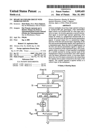
  • 1. United States Patent (19) Himida et al. (54) BINARY MULTIPLIER CIRCUIT WITH IMPROVED INPUTS Hedi Hmida, Paris; Pierre Duhamel, Issy les Moulineaux, both of France 75 Inventors: 73 Assignee: Etat Francais represente par le Ministre Delegue des Postes et Telecommunications (Centre National d'Etudes des Telecommunications), Issy les Moulineaux, France 21 Appl. No.: 578,201 22 Filed: Sep. 6, 1990 Related U.S. Application Data 62 Division ofSer. No. 248,089, Sep. 23, 1988. (30) Foreign Application Priority Data Sep. 23, 1987 FR France ................................ 87 346 51) Int. Cl............................ G06F 7/52; G06F 7/50 52 U.S.C. ..................................... 364/757; 364/786 58 Field of Search ................ 364/754, 757,784, 786 56) References Cited U.S. PATENT DOCUMENTS 4,853,887 8/1989 Jutand et al. ........................ 364/757 4,985,862 l/1991 Hnida et al. ....................... 364/786 (fixed B) Di ||||||||||||I|| USOO5095455A 11 Patent Number: 45 Date of Patent: 5,095,455 Mar. 10, 1992 Primary Examiner-Heather R. Herndon Assistant Examiner-Long T. Nguyen Attorney, Agent, or Firm-Foley & Lardner 57 ABSTRACT Abinary multiplier circuit hasalogic operatoractingas an exclusive-OR gate generating a first intermediate signal which is an exclusive-OR of a first input and a carry-in input. An inverter generates a second interme diate signal. A second logic operator generates a first output bit which is a symmetrical exclusive-OR of a second input and both the first and second intermediate signals. A second output bit is a symmetrical trigger function ofthe first and second input, depending on the firstandsecond intermediatesignals,and is generated in a transmission gate. Since the carry-in signal passed via the first and second intermediate signals is applied di rectlytotransistorsofthetransmission gate, carryprop agation delay is reduced. A fixed operand is multiplied by a variable operand by storing a partial result ofthe multiplication using an accumulator and a shift register with the binary calculation circuit. A two-input multi plexerhasoneofitsinputsconnectedto theoutputfrom the register and an output connected to the input ofthe register. The variable operand is applied serially to a control input ofthe multiplexer. 5 Claims, 6 Drawing Sheets Accumulator and Shift reqister
  • 2. 5,095,455 Sheet 1 of 6 Mar. 10, 1992 U.S. Patent wzºu,i----|---------------+---------«-»-,
  • 3. Sheet 2 of 6 5,095,455 Mar. 10, 1992 U.S. Patent | | | | | | | | | | h S K - - - - - ----------
  • 4. U.S. Patent Mar. 10, 1992 Sheet 3 of 6 5,095,455 ---- - - -- - - - -- - - - - - - - - - -------- V 40B 201B Ri-1S) O3B i) 402B 202B V3B 2 (Ri-1S) -l 2 ---its----------------- la) RS)
  • 5. U.S. Patent Mar. 10, 1992 Sheet 4 of 6 5,095,455 3C 2. (RS) - - - - - - - - - - - - - - - - - - - - - - - - - - - - - 2C (Ai)
  • 6. Sheet 5 of 6 5,095,455 Mar. 10, 1992 U.S. Patent 000Z ! [] S
  • 7. U.S. Patent Mar. 10, 1992 Sheet 6 of 6 5,095,455 (fixed B) Multiplexer Accumulator Shift reoister Di FIG.8
  • 8. 5,095,455 1. BINARY MULTIPLER CIRCUIT WITH IMPROVED INPUTS This application is a division ofapplication Ser. No. 07/248,089, filed Sept. 23, 1988. The invention relates to calculations on binary digits, i.e. bits. It is applicable to realizing binary electronic systems such asadders, multipliers, dividers, accumula torS, . . . . BACKGROUND OF THE INVENTION The document "Proceedings of the IEEE Interna tional Conference on Computer Design: VLSI in Com puters", New York, Oct. 7-10, 1985, pp. 359-362; S. Steinlechner, and our prior French patent application number 87 03758 filed Mar. 18, 1987 (and our corre sponding U.S. patent application Ser. No. 167,787) de scribe a binary calculation circuit ofthe type compris ing at least one cell having: a 1-bitfirstinputfor receivinga firstinputsignal (Ai); a 1-bit second input for receiving a second input sig nal (Bi); a 1-bit carry-in input for receiving a carry-in signal (Ri-1 S); first means for generating an exclusive-OR signal (AiGDBi) and its complement (AieeBi) from the firstand Second input signals; second means for producing a result signal by per formingan exclusive-OR function between the carry-in signal (Ri-1 S) said exclusive-OR signal (AieBi); third meansforproducinga carry-out signal (RiS)by performing a transmission function by means of two transmission gates controlled by said exclusive-OR sig nal (AieBi) and its complement (AieeBi), with one of the gates passing the carry-in signal (Ri-1 S) and the other gate passing one or other ofthe two input signals (Ai, Bi). In the embodiments described in the earlier patent application, the carry-in signal (Ri-1 S) is applied to the drainsofthetransistorsequippingthetransmission gates under the control ofsaid exclusive-OR signal (AieBi) and its complement (AieBi). This gives riseto a loss of time during calculation of the carry-out signal (Ri S) and consequently to a loss ofcarry propagation time in circuits comprising a plurality ofcells in parallel orga nized as adder and/or subtracter modules with propa gated carry. The Applicants have now observed that by inter changing the roles of the second input signal (Bi) and the carry-in signal (Ri-1 S), and by using the intermedi ate variables thus obtained by said interchange for cal culating the carry-out signal (RiS), the carry propaga tion delay in such parallel-connected cells is considera bly reduced. The carry-in signal (Ri-1 S)passingviathe exclusive-OR signal (Aieri-1 S) is now applied di rectly to the grids ofthe transistors in the transmission gates which are controlled by said exclusive-OR signal (Aieri-1 S) and its complement (AieeRi-1S). SUMMARY OF THE INVENTION More precisely, the present invention provides a bi nary calculation circuit ofthe type comprising at least one cell having: a 1-bitfirstinputfor receivinga firstinput signal (Ai); a 1-bit second input for receiving a second input sig nal (Bi); and 5 O 15 20 25 30 35 40 45 50 55 65 2 a 1-bit carry-in input for receiving a carry-in signal (Ri-1 S); comprising: first means for generating an exclusive-OR signal (AieRi-1 S) between the first input signal and the car ry-in signal, and the complement thereof(AiGDR-1S), said complement (AieeRi-1 S) being produced by in verting the signal (AieeRi-1 S); second means for producing a result signal by per forming an exclusive-OR function between the second inputsignal (Bi) andsaid exclusive-ORsignal (AieRi-1 S) between the first input signal and the carry-in signal; and third meansforproducingacarry-outsignal (RiS)by means ofa transmission function comprising two trans mission gates controlled by said exclusive-OR signal (Aieri-1 S) between the first input signal and the car ry-in signal, and the complement thereof (Aieri-1 S), with one ofthe gates passing the first input signal (Ai) and with the other gate passing the second input signal (Bi). In a preferred embodiment ofthe invention, the first, second, and third means are connected in the same manner as the first, second, and third means respec tively as claimed in any ofthe claims ofour above-men tioned earlier patent application, with the 1-bit second input (Bi) and the 1-bit carry-in input (Ri-1 S) being interchanged. The invention also provides a binary calculation cir cuit of the type comprising at least one basic cell for adding a first bit (Ai) of arbitrary binary value taken from a variable operand (A) anda secondbit (Bi) whose binary value is fixed and known taken from a fixed operand (B), whereineach cell comprisesafirst module for delivering an exclusive-OR signal (AieeRi-1 S) be tween the first input signal and the carry-in signal, and a second module for producing a carry-out signal (RiS) by performing a transmission function comprising two transmission gates under the control of the carry-in signal (Ri-1 S) and its complement (Ri-1 S), with one of the gates passing the first input signal (Ai) and with the other gate passing the second input signal (Bi). In a preferred embodiment, the binary calculation circuit according to the invention comprises a plurality of cells in which the carry-out signal (RiS) from each cell of rank (i) (0<ian-2) is connected to the 1-bit carry-in input (RiS) of the cell of rank i-1. Advanta geously, each cell is hard-wired with the valueofthebit (Bi) ofthe fixed operand B. Moreparticularly, thefirst module ofeach cell which is associated with a bit (Bi) of logic value "0" of the fixed operand (B) comprisesthree pairs oftransistors as follows: a first pair ofopposite polarity transistorscomprising a first transistor and a second transistor, with the grids ofboth transistors in the first pair being connected to receivethe carry-insignal(Ri-1 S),withapositiveelec tric voltage (V) being applied to the drain of the first transistor, with ground being applied to the source of the second transistor, and with the source of the first transistor and the drain of the second transistor being interconnected at a first node; a second pair of opposite polarity transistors, con prising a first transistorandasecond transistor, with the drain of the first transistor being connected to receive the carry-in signal (Ri-1 S), with the source ofthe sec ond transistor being connected to the first node, with the gridsofboth transistorsbeingconnected to receive
  • 9. 3 thefirstinputsignal (Ai)from the variable operand (A), and with the source of the first transistor and the drain ofthe second transistor being interconnected at a sec ond node; and a third pair ofopposite polarity transistors, compris ing a first transistor and a second transistor, with the sources of both transistors being connected to the second node, with the drains of both transistors being connected to receive thefirst inputsignal (Ai) from the variable operand (A), with the grid ofthe first transis tor being connected to receive the carry-in signal (Ri-1 S), and with the grid of the second transistor being connected to the first node, such that said exclu sive-OR signal (AieRi-1 S) between the bits of the variable operand (A) and the carry-in signal is obtained at the second node. According to another aspect of the invention, the second module of each cell asssociated with a bit (Bi) oflogic value "O" in the fixed operand (B) comprises: a fourth pair of opposite polarity transistors, com prising a first transistor and a second transistor, with the grid of the first transistor being connected to receive the carry-in signal (Ri-1 S), with the grid ofthe second transistor being connected to receive the con plemented carry-in signal (Ri-1 S), with the drains of both transistors being connected to receive the first input signal (Ai) from the variable operand (A), and with the sources ofboth transistors being connected to a third node; and a single third transistor which is an N-channel tran sistor with itssourceconnected to ground, with its grid controlled by the complemented carry-in signal Ei S), and with its drain connected to the third node, the carry-out signal (RiS) beingobtained at the third node interconnecting the sources of both transistors in the fourth pair with the drain ofthe third transistor. According to another aspect of the invention, the first module of each cell associated with a bit (Bi) of logic value "1" of the fixed operand (B) comprises three pairs oftransistors as follows: a first pair ofopposite polarity transistors comprising a first transistor and a second transistor, with the grids ofboth transistors in the first pair being connected to receive the carry-in signal (Ri-1 S), with a positive electric voltage (V) being applied to the drain of the first transistor, with ground being applied to the source ofthesecond transistor, and with the source ofthefirst transistor and the drain of the second transistor being interconnected at a first node; a second pair of opposite polarity transistors, com prising a first transistor and a second transistor, with the drain of the first transistor being connected to the first node, with the source of the second transistor being connected to receive the carry-in signal (Ri-1 S), with the grids of both transistors being connected to receive the first input signal (Ai) from the variable operand (A), and with the soruce ofthe first transistor and the drain of the second transistor being intercon nected at a second node; and a third pair ofopposite polarity transistors, compris ing a first transistor and a second transistor, with the sources of both transistors being connected to the second node, with the drains ofboth transistors being connected to receivethe first inputsignal (Ai)from the variable operand (A), with the grid ofthe first transis torbeingconnected to the first node, and with thegrid ofthe second transistor being connected to the carry-in input (Ri-1 S), such that the exclusive-OR signal (AieeRi-1 S) between the bits ofthe variable operand 5,095,455 5 10 15 20 25 30 35 45 50 55 65 4. (A) and the carry-in signal is obtained at the second node. Accordingto yet another aspectoftheinvention, the second module ofeach cell associated with a bit (Bi) of logic value "1" in the fixed operand (B) comprises: afourth pair ofoppositepolaritytransistors, compris ing a first transistor and a second transistor, with the grid ofthefirsttransistorbeingconnected to receivethe carry-in signal (Ri-1 S), with the grid of the second transistorbeingconnectedto receivethe complemented carry-in signal (Ri-1 S), with the drains ofboth transis tors being connected to receive the first input signal (Ai) from the variable operand (A), and with the sources of both transistors being connected to a third node; and a single third transistor which is a P-channel transis tor with itssource connected to a positive electric volt age (V), with its grid controlled by the complemented carry-in signal (Ri-1 S), and with its drain connected to the third node, the carry-out signal (Ri S) being ob tained at the third node interconnecting the sources of both transistors in the fourth pair with the drain ofthe third transistor. The invention may also be applied to aparallel-series binary multiplier for multiplying a fixed operand B comprising nbits Bn-1, Bn-2,..., B0bya variable n-bit operand D ofarbitrary value having bits Dn-1, Dn-2, . . . , D0, said multiplier including an accumulator and shift registerforstoringapartial result ofthemultiplica tion, said register including an input and an output. A particular multiplier of this type is described in French patent application number 86 13222. According to another characteristic of the present invention, the multiplier further includes: a binarycalculation circuitasdescribedaboveinclud ing and output and an input connected to the output of the register, each cell ofsaid binary calculation circuit including a first module for delivering an exclusive-OR signal (DieRi-1 S) and a second module for producing a carry-out signal (RiS); and a two-input multiplexer having one of its inputs connected to the output from the binary calculation circuit and having its other input connected to the output from the register, and having an output connected to the input of the register, said multiplexer also including a control input to which the variable operand D is applied in serial form. In a variant embodiment, forthe purposeofmultiply ing two opposite-sign operands, the multiplier further includes a second multiplexer disposed between the output from the accumulator and shift register and the input to the adder, said second multiplexer having two inputs, one connected to the output from the register and the other connected to the output of an inverter whose input is connected to the output from the regis ter, said second multiplexer being controlled by the most significant bit Dn-1 ofthe operand D. BRIEF DESCRIPTION OF THE DRAWINGS Embodiments ofthe invention are described by way ofexample with reference to theaccompanying draw ings, in which: FIG. 1 isacircuitdiagram oftheessential component parts ofa full adder in accordance with the invention having three 1-bit inputs (Ai, Bi, and Ri-1 S) andcom prising 16 transistors; FIG.2isacircuitdiagramoftheessentialcomponent parts ofa full adder in accordance with the invention
  • 10. 5,095,455 5 having three 1-bit inputs (Ai, Bi, and Ri-S) and com prising 15 transistors; FIG. 3 is a circuit diagram of two modules of an addition cell in accordance with the invention for add ing a bit (Ai) ofarbitrary binary value to a bit oflogic value "0"; FIG. 4 is a circuit diagram of two modules of an addition cell in accordance with the invention for add ing a bit (Ai) ofarbitrary binary value to a bit oflogic value "1": FIG. 5 is a diagram ofa circuit in accordance with the invention capable of being configures as either of the cells described with reference to FIGS. 3 and 4, with its inputs being programmable as a function ofthe fixed operand B; FIG. 6 is a block diagram ofan adder in accordance with the invention in which the addition cells are hard wired with the values ofthe bits ofthe fixed operand; FIG. 7 is a diagram ofthe structure ofa multiplier in accordancewith theinvention,said multiplierincluding an adder in accordance with FIG. 6; and FIG. 8 showsa variant embodiment ofthe multiplier in accordance with the invention, for processing two operands of arbitrary sign. In numerous respects, the accompanying drawings include information which is definitive in nature. Con sequently, they may be used not only for facilitating understanding ofthefollowingdetailed description, but also for contributing to the definition of the invention, where appropriate. MORE DETAILED DESCRIPTION In FIG. 1, reference 2A designates a full adder in accordance with the invention having three 1-bit inputs and comprising 16 transistors. The addition cell 2A shown in FIG. 1 is practically identical to the addition cell 2 shown in FIG. 2 of our above-mentioned prior patent application. It differs solely in that the second 1-bit input (Bi) has been inter changed with the 1-bit carry-in input (Ri-1 S), and in that the letter A has been added to the references ofthe essential component parts of adder 2A in accordance with the present invention. The adder 2A includes a 1-bit first input (Ai), a 1-bit second input (Bi), and a 1-bit carry-in input (Ri-1 S). The adder 2A produces a 1-bit result signal (Si). The result is the sum ofthe two bits (Ai, Bi) and the carry-in bit (Ri-1 S). It is obtained by calculating the modulo sun, also known as the exclusive-OR sum, of the first bit (Ai), the second bit (Bi),and the carry-in bit (Ri-1 S). Theadder 2A produces a 1-bit carry-outsignal (RiS) which is associated with the result of calculating the sum (Si) ofthe three input signals (Ai, Bi, and Ri-1 S). The carry-out signal (RiS) is obtained by calculating the sum of the product ofthe two input bits; the prod uct ofoneoftheinputbits (Ai) and the carry-inbit (Ri-1 S), and the product of the other input bit (Bi) and the carry-in bit (Ri-1 S). In order to obtain these two signals, the adder 2A comprisesfirst means 100A forgeneratingan exclusive OR signal (AieRi-1 S) between a first one ofthe input signals (Ai) and the carry-in signal. These first means 100A comprise a pair ofcomplementary MOS technol ogy transistors 101A and 102A. Transistor 101A is a P-channel device and transistor 102A is an N-channel device. Thegrids ofboth transistors 101Aand 102A are connected to the firstbit input (Ai). An electric voltage V is applied to the drain D of transistor 101A. For O 15 25 35 45 50 55 6 example, when the transistors are MOS technology devices, the value ofV may be 5 volts. Ground is con nected to the source S oftransistor 102A. The source of transistor 101A and the drain of transistor 102A are interconnected at a node 103A. The first means 100A alsoincludeasecond pair ofcomplementaryMOStech nology transistors 104A and 105A. Transistor 104A is P-channel and transistor 105A is N-channel. The drain oftransistor 104is connected to the 1-bit first input (Ai) and the source of transistor 105A is connected to the node 103A. The grids ofthe transistors 104A and 105A are connected to the 1-bit carry-in input (Ri-1 S). The source of transistor 104A and the drain of transistor 105A are interconnected at a node 106A. The first means 100A further include a third pair of complementary transistors 107A and 108A. Transistor 107A is P-channel and transistor 108A is N-channel. The sources of transistors 107A and 108A are con nected to the node 106A. The drains oftransistors 107A and 108Aare connected to the 1-bitcarry-in input (Ri-1 S). The grid oftransistor 107A isconnected to the 1-bit first input (Ai) and the grid of transistor 108A is con nected to the node 103A. The exclusive-OR signal (AieRi-1 S) between the first input signal and the car ry-in signal is obtained at the node 106A. The first means 100A operate as follows: When thefirstinputsignal (Ai)isat apositive voltage V corresponding to a high logicstate, transistor 101A is OFF, whereas transistor 102A is ON. In this configura tion, a Zero voltage, corresponding to a low logic state, is obtained at the node 103A. When the first input signal (Ai) is at a zero voltage, transistor 101A is ON, whereas transistor 102A is OFF. In this case, a positive electric voltageis obtained at the node 103A. The pair oftransistors 101A and 102A acts as an inverter on the first input signal (Ai). When the first bit signal (Ai)isin thehigh logicstate, the complemented signal (Ai) is in the low logic state. The pair of transistors 104A and 105A also acts as an inverter, thus causing the complemented signal (Ri-1S) appear at node 106A. The transmission gate constituted by the pair oftransistors 107A and 108A is open. When the first input signal (Ai) is in the low logic state, the complemented signal (Ai) is in the high logic state. The transmission gate constituted by the pair of transistors 107A and 108A is now closed, thus causing the carry-in signal (Ri-1 S) to pass to the node 106A. The pair oftransistors 104A and 105A is inactive. As a result, the signal at node 106A is the exclusive-OR sig nal (AieRi-1 S) between the first input signal and the carry-in signal. The adder then comprises a pair 400A of opposite polarity transistors 401A and 402A. This pair inverts said exclusive-OR signal (Aieri-1 S) between the first input signal and the carry-in signal. The transistor pair 400A comprises a P-channel transistor 401A and an N-channel transistor 402A. The grids ofthe transistors 401A and 402A are connected to receive the exclusive OR signal (Aieri-1 S) between the first input signal and the carry-in signal. An electric voltage V is applied to the drain oftransistor 401A. When using MOS tech nologytransistors, Vhasavalue of5 volts,for example. Ground is applied to the source oftransistor 402A.The complemented exclusive-OR signal (AiR-1 S) be tween the first input signal and the carry-in signal is obtained at node403A connecting thesource oftransis tor 401A to the drain of transistor 402A. The pair of
  • 11. 5,095,455 7 transistors 401A and 402A operates in the same way as the above-described pair oftransistors 101A and 102A. The adder 2A then comprisessecond means 200A for producing a result signal (Si) by performing the exclu sive-OR function between the second input signal (Bi) and said exclusive-OR signal (AieeRi-1 S) between the first input signal and the carry-in signal and with the complement thereof(AieRi-1 S). These second means 200A comprise two pairs of opposite polarity transis tors.Thefirstpairisconstituted by transistors201A and 202A. Transistor 201A is P-channel and transistor 202A isN-channel.Thegridsofthetransistor201Aand202A are connected to the 1-bit second input (Bi). The drain oftransistor 201A is connected to receive the exclusive OR signal (AiR-1 S) between the first input signal and the carry-in signal. The source oftransistor201Ais connected to the complemented exclusive-OR signal (AieRi-1 S)between the first input bitand thecarry-in signal. The result signal (Si) is obtained at a node 203A 10 5 connecting thesource oftransistor 201A to the drain of 20 transistor 202A. The second pair is constituted by transistors 204A and 205A. Transistor 204A is P-channel and transistor 205A is N-channel. The drains ofboth transistors 204A and 205A are connected to the 1-bit second input (Bi). The grid oftransistor204A is connected to receivesaid exclusive-OR signal (AiGRi-1 S) between the first input signal and the carry-in signal. The grid oftransis tor 205A is connected to the complemented exclusive OR signal (AiR-1 S) between the first input signal and the carry-in signal. The result signal (Si)is obtained from the node 203A interconnecting the sources ofthe transistors 204A and 205A. The second means 200A operate as follows: When said exclusive-OR signal (AieRi-1 S)between thefirstinput signaland thecarry-in signalisin thehigh logic state, the complemented signal (AiéRi-S) is in the low logic state. The pair of transistors 201A and 202A acts as an inverter causing the complemented signal (Bi) to appear at node 203A. The transmission gate constituted by the pair of transistors 204A and 205A is open. Whensaid exclusive-ORsignal (AiGRi-1S)between the first input signal and the carry-in signal is in the low logic state, the complemented signal (AiGRi-1 S) is in the high logic state. The transmission gate constituted by the pair oftransistors 204A and 205A is now closed, thus causing the second signal (Bi) to appear at node 203A.Thepair oftransistors201A and 202Aisinactive. Finally, the adder includes third means 300A for producing a carry-out signal (RiS) by means ofa trans mission function comprising two transmission gates underthecontrol ofsaid exclusive-ORsignal (AieeRi-1 S) between the first input signal and the carry-in signal 25 30 35 45 50 and under the control of its complement, with one of 55 the gates passingthe first input signal (Ai) and with the other gate passing the second input signal (Bi). Thethird means300Acomprisetwopairsofopposite polarity transistors. Thefirst pairisconstituted by tran sistors 301A and 302A. Transistor 301A is N-channel and transistor302A is P-channel. The grid oftransistor 301A is connected to receive the complemented exclu sive-OR signal (AiR-1 S) between the first input signal and the carry-in signal. The grid of transistor 302A is connected to theexclusive-ORsignal (AieeRi-1 S) between the first input signal and the carry-in signal. The drains of transistors 301A and 302A are connected to the 1-bit first input (Ai). The carry-out signal (RiS) 65 8 is obtained at the node 303A interconnecting the sources of transistors 301A and 302A. The second pair is constituted by transistors304A and 305A. Transistor 304A is P-channel and transistor 305A is N-channel. The grid oftransistor 304A is connected to receive the complement of the exclusive-OR signal (AieRi-1 S) between the first input signal and the carry-in signal. The grid oftransistor 305A is connected to receive the exclusive-OR signal (AieRi-1S) between the first input signal andthe carry-in signal. Thesources ofboth transistors 304A and 305A are connected to the 1-bit second input (Bi). The carry-out signal (Ri S) is ob tained at the node303A which interconnects the drains of transistors 304A and 305A. The third means 300A operate as follows: When the exclusive-OR signal (AieRi-1 S) between the first input signal andthecarry-in signal isin the low logic state, the complemented signal (AiR-1 S) is in the high state. The transmission gate constituted by the transistors 301A and 302A is closed causing the signal (Ai) to appear at node 303A. The transmission gate constituted by the pair oftransistors 304A and 305A is inactive. When the exclusive-OR signal (Aieri-1 S) between thefirstinputsignalandthecarry-insignal isin thehigh logic state, the complemented signal (AiéRi-1 S) is in the low state. The transmission gate constituted by transistors 304A and 305A is now closed, causing the second input signal (Bi) to appear at node 303A. The pair oftransistors 301A and 302A is inactive. It will be observed that in the above-described 16 transistor adder 2A, thegrids oftransistors 301A,302A, 304A, and 305A now have the carry-in signal (Ri-1 S) applied thereto (or more precisely the exclusive-OR signal (AieeRi-1 S) and its complement (AiR-1 S) between the first input signal and the carry-in signal). This structure thus serves to accelerate carry propaga tion through a binary calculation circuit in accordance with the invention and comprising a plurality ofaddi tion cells as described with reference to FIG. 1, with the carry-out signal (Ri S) from each cell of rank (i) (0<i{n-2)being connected to the carry-in input (RiS) of the cell of rank (i+1). Reference is now made to FIG. 2 which is a circuit diagramofafulladderinaccordancewiththeinvention having three 1-bit inputs and comprising 15 transistors. The addition cell 4A shown in FIG. 2 is practically identical to the addition cell 4 shown in FIG. 3 of our above-mentioned earlier patent application. It differs solely in that the 1-bit second input (Bi) isinterchanged with the 1-bit carry-in input (Ri-1 S), and in that the letter A is added to the references ofthe essential com ponentpartsofadder4Ainaccordancewiththepresent invention. In order to obtain an adder 4A comprising only 15 transistors, the first means 100A of adder 2A as de scribed with reference to FIG. 1 are modified. The othermeans250A,350A,andthepair450Aoftheadder 4A are respectively identical to the means 200A, 300A, and 400A ofadder 2A described with reference to FIG. 1. The first means 109A ofadder 4A comprise a pair of P-channel transistors 110A and 111A. The grid oftran sistor 110A is connected to the 1-bit first input (Ai) and the grid of transistor 111A is connected to the 1-bit carry-in input (Ri-1 S). An electrical voltage V is ap plied to the drain oftransistor 110A. When using MOS technology transistors, V may have a value of 5 volts,
  • 12. 5,095,455 forexample.Thesource oftransistor 110A is connected to the drain oftransistor 111A. The source oftransistor 111A is connected to a node 112A. The first means 109A ofadder4A comprise a further pairoftransistorsconstitutedbyan N-channel transistor 113A and an N-channel transistor 114A. The source of transistor 113A is connected to the 1-bit first input (Ai). The grid of transistor 113A is connected to the 1-bit carry-in input (Ri-1S). The source oftransistor 114A is connected to the carry-in input (Ri-1 S). The grid of transistor 114A is connected to the first bit input (Ai). The complemented exclusive-OR signal (AieRi-1 S) between the first input bit and the carry-in signal is obtainedat node 112A connecting thesource oftransis tor 113A to the drain of transistor 114A. The first means 109A of adder 4A finally include a single P-channel transistor 115A. The source oftransis tor 115A is connected to node 112A. An electric volt age V is applied to the drain of transistor 115A. The grid oftransistor115A is connected to node453A ofthe pair 450A constituted by transistors 451A and 452A identical to the pair400A oftransistors401A and402A described with reference to FIG. 1. The function of transistor 115A is to put the complement (AiéRi-1 S) via node 112A to the high logic state when the transis tor 115A is activated, i.e. when the signal (AieeRi-1 S) applied tothe grid oftransistor 115A isin the low logic State. Naturally, interchanging the 1-bit second input (Bi) 10 15 10 The first module 3B comprises a pair of transistors 401B and 402B which are respectively P-channel and N-channel. Thegridsofboth transistors401B and402B are connected to the 1-bit carry-in input (Ri-1 S). A positive electric voltage V is applied to the drain of transistor 401B, and ground is applied to the source of transistor 402B. The source of transistor 401B and the drain of transistor 402B are interconnected at a node 403B. The module 3B includes a further pair oftransis tors 201B and 202B which are respectively P-channel and N-channel. The drain of transistor 201B is con nected tothe 1-bitcarry-in input(Ri-1S)andthesource oftransistor 202B is connected to node 403B. The grids of both transistors 201B and 202B are connected to the 1-bit first input (Ai) from the variable operand A. The source of transistor 201B and the drain of transistor 202B are interconnected at another node 203B. The module 3B also includes a pair oftransistors 204B and 20 25 with the 1-bit carry-in input (Ri-1 S) for the purpose of 30 accelerating carry propagation in successive cells may beperformed in various propagated carry binary calcu lation circuits such as the adders and subtracters de scribed in our prior application. The adders 2A and 4A as described above constitute a first type ofembodiment oftheinvention. Some ofthe means ofthese adders may advantageously be used for constituting a binary calculation circuit of the type includingat least onebasic cell for addingafirst bit (Ai) from a first, variable operand A of arbitrary binary value with a second bit (Bi) from a second, fixed oper and B whose binary value is known. Naturally, the specific value of the fixed operand determinesthestructureofeach cell ofabinary calcula tion circuit for adding a fixed operand ofknown value with an operand of arbitrary value. Thus, in a binary calculation circuit in accordance with the invention, there are two types ofcell: cells associated with a fixed operand bit having logic value "O'; and cells associated with a fixed operand bit having logic value "1". Reference is now made to FIG. 3 which shows one cell of a binary calculation circuit associated with a fixed operand of logic value '0'. Advantageously, the cell 2B is derived from the cell 2A described with refer 35 45 205B which are respectively P-channel and N-channel. The sources ofboth transistors 204B and 205B are con nected to said other node 203B. The drains of both transistors 204B and 205B are connected to receive the first input signal (Ai) from the variable operand A. The grid oftransistor 204B is connected to the 1-bit carry-in input (Ri-1 S) and the grid of transistor 205B is con nected to one of the nodes 403B. The exclusive-OR signal (AieRi-1 S) between the first input signal ofthe operand A and the carry-in signal is obtained at node 203B. Module 3B operates identically to the means 400A and 200A described with reference to FIG. 1. The second module 5B of cell 2B associated with a "O" logic value bit (Bi) from the fixed operand B com prises a pair of transistors 301B and 302B which are respectivelyN-channeland P-channel. Thegridoftran sistor 301B is connected to receive the carry-in signal (Ri-1 S), and the grid oftransistor 302B is connected to receive the complemented carry-in signal (Ri-1 S). The drains of both transistors 301B and 302B are connected to receive the first input signal (Ai) from the variable operand A. The sources of both transistors 301B and 302B are connected to a node 303B. Thesecond module 5B includes a further N-channel transistor 305B whose source isconnected to ground, whose grid is controlled by the complemented carry-in signal (Ri-1 S), and whose drain is connected to node 303B. The carry-out signal (RiS) is obtained at node 303B interconnecting the drain oftransistor 305B and the sources ofthe tran 50 ence to FIG. 1 by omitting the means 100A and one of 55 the transistors in the means 300A, by modifying the inputs, and by addinga B to the references ofthe essen tial component parts ofthe cell 2B in accordance with the invention. The cell 2B comprises a first module 3B for deliver ing the exclusive-OR signal (AieRi-1 S) between the first input signal and the carry-in signal, and a second module 4B forproducing the carry-out signal (RiS) by means ofa transmission function comprising two trans mission gates controlled by the carry-in signal (Ri-1 S) anditscomplement(Ri-1 S), withone ofthegatespass ing the variable input signal (Ai) and the other gate passing the fixed operand bit of logic value "0". 65 sistor 301B and 302B. The module 5B operatesas follows. When the carry in signal (Ri-1 S) is in the high logic state, the comple mented carry-in signal (Ri-1 S) is in the low state. The transmission gate constituted by the transistors 301B and302B is closed, causingthe first input signal (Ai) to appear at node303B. The transmission gate constituted by transistor 305B is inactive. When the carry-in signal (Ri-1 S) is in the low logic state, the complemented signal(Ri-1 S)isinthehighstate.Thetransmissiongate constituted by the transistor 305B is now closed, caus ingthegroundsignal, i.e. the second inputsignal (Bi) of logic value "0" to appear at node 303B. The pair of transistors 301B and 302B is inactive. Reference is now made to FIG. 4 which shows an addition cell 2C for adding a first bit (Ai) from the variable operand A of arbitrary binary value with a second bit (Bi) from the second operand B of fixed binary value equal to "1'. The cell 2C comprises a first module 3C for deliver ing an exclusive-OR signal (AieRi-1 S) between the
  • 13. 5,095,455 11 first input signal and the carry-in signal, and a second module 5C for producing a carry-out signal (RiS) by means ofa transmission function comprising two trans mission gates controlled by the carry-in signal (Ri-1 S) and its complement (R-1 S), with one ofthe gatespass ing the variable or first input signal (Ai) and with the other gate passing the bit ofthe fixed operand oflogic value '1'. The module 3C comprises a pair of transistors 401C and 402C which are respectively P-channel and N channel. The grids ofboth transistors 401C and 402C are connected to the 1-bit carry-in input (Ri-1 S). A positive electric voltage V is applied to the drain of transistor 401C, with ground being applied to the source oftransistor 402C. The source oftransistor401C and the drain of transistor 402C are interconnected at the node 403C. The module 3C further includes a pair of transistors 201C and 202C which are respectively P-channel and N-channel. The drain of transistor 2010 is connected to node 403C and the source of transistor 202C is connected to the 1-bit carry-in input (Ri-1 S). The grids of both transistors 201C and 202C are con nected to the 1-bit first input (Ai) from the variable operand A. Thesource oftransistor201C and the drain oftransistor 202C are connected to the node 203C. The module 3C finally includes a pair of transistors 204C and 205C which are respectively P-channel and N channel. The sources ofboth transistors 204C and 205C are connected to node 203C. The drains ofboth transis tors204Cand205Care connectedtothe 1-bitfirst input (Ai) from the variable operandA.Thegrid oftransistor 204C is connected to node 403Cand the grid oftransis tor 205C is connected to the 1-bit carry-in input (Ri-1 S).Theexclusive-ORsignalbetween thebitoftheoper and A and the carry-in signal (Ri-1 S) is obtained at node 203C. Module 3C operates in exactly the same way as the means 450A and 200A described with reference to FIGS. 1 and 2. The second module 5C ofaddition cell 2C includes a pair of transistors 301C and 302C which are respec tively P-channel and N-channel. The grid oftransistor 301Cisconnected to receivethe carry-insignal (Ri-1 S) and the grid oftransistor 302C is connected to receive the complement of the carry-in signal (Ri-1 S). The drains ofboth transistors 301C and 302C are connected to receive the first input signal (Ai) from the variable operand A, and thesources ofboth transistors301Cand 302C are connected to a node 303C. The nodule 5C further includes a P-channel transistor 304C whose source is connected to a positive electric voltage V, whose grid is controlled by the complemented carry-in signal (Ri-1 S)and whosedrainisconnected tothe node 303C. The carry-out signal (Ri S) is obtained at node 303C interconnecting the sources of both transistors 301C and 302C with the drain oftransistor 304C. Module 5C operates as follows: when the carry-in signal (Ri-1 S) is in the low logic state the comple mented carry-insignal (Ril S) isin the high state.The transmission gate constituted by the transistors 301C and 302C is closed causing the signal (Ai) to appear at node 303C. The transmission gate constituted by the transistor 304C is inactive. When the carry-in signal (Ri-1 S) is in the high logic state, its complement E. S) is in the low logic state. The transmission gate constituted by transistor304C is now closed, causing the signal at voltage V, i.e. the second input signal (Bi) oflogic value "1" to appear at 10 5 20 25 30 35 45 50 55 60 65 12 node 303C. The transmission gate constituted by the transistors 301C and 302C is inactive. It may be observed that either ofthese two cells may be made from a single programmable circuit with the value taken by the fixed operand (Bi) depending on its metallization, i.e. on how the inputs to the single pro grammable circuit are connected. Reference is now made to FIG. 5 which illustrates how toprogram theinputsofsuch asingleprogramma blecircuit.Thisfigureshowsthethreeessentialcompo nent parts of an adder, one of whose operands has a value which is fixed and known. Such a programmable input adder2D uses thesame essential parts as the pre ceding adders 2B and 2C, with equivalent references nowbeingfollowedbya D.Themeans300Dareidenti cal to the means 300A described with reference to FIG. 1. They differ only in the signals which are applied to the grids and to the drains ofthe transistors. For a fixed operand oflogic value equal to "0", the grid oftransistor 304D receives an electric voltage of potential V (X=V). The grid of transistor 305D re ceives the complemented carry-in signal (Ri-1 S), (Y=(Ri-1 S)). The grid oftransistor301D receives the complemented carry-in signal (R-1S), (Z=(R-1 S). The grid oftransistor 302D receives the carry-in signal (Ri-1S),(T=(Ri-1 S)).Thedrain oftransistor201Dand the grid of transistor 204D receive the carry-in signal (Ri-1 S), (C=(Ri-1 S)). The source of transistor 202D and the grid of transistor 205D receive the comple mented carry-in signal (Ri-1 S), (D=(Ri-1 S)). For a fixed operand oflogic value equal to "1", the grid oftransistor 304D receives the complemented car ry-in signal (Ri-1 S). The grid of transistor 305D is connected to ground. The grid of transistor 301D re ceivesthe carry-in signal (Ri-1S). The grid oftransistor 302D receives the complemented carry-in signal (Ri-1 S). The drain oftransistor 301D and the grid oftransis to 304D receive the complemented carry-in signal (Ri-1 S). The source oftransistor 302D and the grid of transistor 305D receive the carry-in signal (Ri-1 S). Reference is now made to FIG. 6 which shows an adderinaccordancewith theinvention comprisingaset of addition cells 2D connected in series. Each cell re ceives one ofthe bits (Ai), for0<i(n-1, ofthe variable operand, i.e. one ofthe bits: An-1, An-2, . . . , A0. Each cell 2D has a specific structure which is pro grammable duringmetallization and which isa function ofthe logic value ofthe known fixed bit (Bi), i.e. Bn-1, Bn-2, ..., B0. Theadders2B, 2C,and2Dasdescribed above consti tute a second type of embodiment of the invention. Theseaddersmayadvantageouslybe used forconstitut ing a binary multiplier for multiplying an operand of arbitrary value with an operand whose value is fixed andknown.Thisconstitutesathirdtypeofembodiment of the invention. Reference is now made to FIG. 7 which shows a binary multiplier in accordance with the invention. It comprisesanadder12inaccordancewiththeinvention, a multiplexer 14, and an accumulator and shift register 16. The items constituting the multiplier have parallel type inputs and outputs. The register 16 has an input and an output. The adder 12 hasan input connected to the output ofregister 16, and it also hasits own output. The adder 12 is as described with reference to FIG. 6 and it differs therefrom solely by the operand A being replacedbyoperand D.Thus,adder12comprisesa first
  • 14. 5,095,455 13 module delivering an exclusive-OR signal (AieRi-1 S) and a second module delivering a carry-out signal (Ri S). The multiplexer 14 has two inputs, one ofits inputs is connected to the output from the adder 12, and its other input is connected to the output from register 16. The output ofmultiplexer 14 is connected to the input of register 16. The fixed operand B is known and is specified by the structure ofadder 12 as described with reference to FIGS. 3 to 6. The variable operand D is applied in serial form to a control input 18 ofthe multi plexer 14. The multiplexer in accordance with the invention operates as follows. At each clock pulse, the adder 12 adds the contents of shift register 16 with the fixed operand B. Ifthe bit (Di) ofranki where 0<i(n-1, of theoperand Dapplied to theinput 18ofthe multiplexer 14 is of value "0", the multiplexer 14 is controlled to select its input which is connected to the output ofthe register 16. The shift register 16 is thus reloaded with the same value as is contained at the preceding instant, but dividedby 2 (shifted). In contrast, ifthebit (Di) has the value "1", the multiplexer connects the input of register 16 to the output of adder 12. In this case, the shift register 16 is reloaded with the result delivered by adder 12. In the embodiment shown in FIG. 7, the adder is capable solely ofadding the contents ofregister 16 with the fixed operand B. If D is a negative number, i.e. (Dn-1=1), it is necessary to subtract the value B from the contents of register 16. This cannot be done with the adder 12 of the multi plexer shown in FIG. 7 since, by construction, it is capable ofadding the single operand B only. In order to circumvent this difficulty, the FIG. 7 multiplier may be modifiedso astobeable toadd in the fixed operand Bwith eithersign. Such a modified multi plier is shown in FIG. 8. In this multiplier, elements which are identical to those ofthe FIG.7 multiplier have thesame references. The FIG. 8 multiplier includes additional elements for inverting the contents ofregister 16. These means com prise an inverter 22 whose input receives the output from register16and a multiplexer20 havingafirstinput connected to the output of register 16 and a second input connected to receive the output from the inverter 22. The output from multiplexer 20 is connected to the input of adder 12. Multiplexer 20 includes a control input 24 for receiving the most significant bit Dn-1 of the serial operand D. The multiplexer 20 thus delivers to the input of adder 12, either the contents ofregister 16 if Dn-1 is equal to "0", or else the complemented contents ofregister 16ifDn-1 is equal to "1". Adder 12 adds the value B to the contents of shift register 16 whose parity is thus determined by the multiplexer 20. The result ofthis sum (the complement ofthe contents of register 16--B) is complemented a second time in orderto obtain the correct result (the contents ofregis ter 16-B). We claim: 1. A parallel-seriesbinarymultiplierfor multiplyinga fixed operand (B)havingnbits (Bn-1, Bn-2,..., BO)by a variable operand (D) having n bits (Dn-1, Dn-2, ..., DO) ofarbitrary value, said multiplier comprising: a binary calculation circuit including an input and an output, saidbinary calculation circuit comprisinga plurality ofcomplementary metal oxide semi-con ductor cells having: O 15 20 25 30 35 45 50 55 65 14 a 1-bit first input for receiving a first input signal Di of arbitrary binary value taken from said variable operand (D), a 1-bit second input for receiving a second bit corre spondingto a bit oflogic value "1" and taken from fixed operand (B), a 1-bit carry-in input for receiving a carry-in input signal (Ri-1 S), a logic inverter means connected to said carry-in input signal, for delivering the complement ofsaid carry-in input signal, a first logic module for generating a first output bit, said first output bit being an exclusive-OR signal (DieRi-1S), representing the symmetrical exclu sive-OR function ofsaid first input signal and said carry-in input signal, a second logic module for generating a carry-out output bit, said carry-out output bit being a logic symmetrical trigger function representing said first input signal depending upon both said carry-in input signal and complemented carry-in input sig nal, said second logic module further comprising: i) a first pair ofopposite polarity transistors form ing a symmetrical source-to-drain arrangement and a symmetrical drain-to-source arrangement, with a gate ofa first transistor ofthe pair being connected to said carry-in inputsignalanda gate ofasecondtransistor ofthepairbeingconnected to said complemented carry-in signal, said source-to-drain arrangement being connected to the first input bit, and said drain-to-source ar rangement delivering said carry-out output bit, and ii) a single transistor which is an N-channel transis tor with its source connected to ground, with its gate controlled by said complemented carry-in input signal, and with its drain delivering said carry-out output bit, a 1-bit first output for receiving said first output bit, and a 1-bit second output for receiving said carry-out output bit, and wherein: a carry-out outputbit (RiS) from each ofsaid cells of a rank (i) (0.<iCn-2) is connected to a carry-in input (R(i+1)-1S) ofa cell ofa rank (i+1), each cell is hardwired for its value ofbit (Bi) from the fixed operand (B), the 1-bit first output from the cell of rank (i) where (i=n-1) is said output from the binary calculation circuit, the 1-bitcarry-in inputfromthecell ofrank,(i)where (i=0) is said input from the binary calculation cir cuit, a two-input multiplexer having one ofits inputs con nected to said output from the binary calculation circuit and having an output, said multiplexer also including a control input to which the variable operand (D) is applied in serial form, and an accumulator and shift register forstoring a partial result ofthe multiplication, said register including aninput connected to theoutput ofthe multiplexer and an output connected to the input ofthe binary calculation circuit and to the other input of the multiplexer. 2. Amultiplexeraccordingtoclaim 1,formultiplying two operands (B) and (D) ofopposite sign, said multi plier further including a second multiplexer disposed between the output from the accumulator and shift
  • 15. 5,095,455 15 register and the input from the binary calculation cir cuit, said second multiplexer having two inputs, one connected to the output from the register and the other connected to the output of an inverter whose input is connected to the output from the register, said second multiplexer being controlled by the most significant bit (Dn-1) ofthe variable operand (D). 3. A multiplieraccordingtoclaim 1, wherein the first logic module of each cell from the binary calculation circuit comprises three pairs oftransistors as follows: a first pairofopposite polarity transistors comprising a first transistor and a second transistor, with the gatesofbothtransistorsbeingconnectedto receive the carry-in signal (Ri-1 S),with apositive electric voltage (V) being applied to the drain ofthe first transistor, with ground beingapplied to the source ofthe second transistor, and with the source ofthe first transistorand the drain ofthesecond transistor being interconnected at a first node; asecond pairofoppositepolaritytransistorscompris ing a first transistor and a second transistor, with the drain ofthe first transistor being connected to receivethe carry-in signal (Ri-1 S), with thesource ofthesecond transistorbeingconnectedto the first node, with the gates ofboth transistors being con nected to receivethefirstinputsignal (Di)fromthe variable operand (D), and with the source of the first transistorand the drain ofthesecond transistor being interconnected at a second node; and a third pair ofopposite polarity transistors, compris ing a first transistor and a second transistor, with the sources ofboth transistors being connected to the second node, with the drain ofboth transistors being connected to receive the first input signal (Di) fromthevariableoperand, with thegate ofthe first transistor being connected to the carry-in input (Ri-1 S), and with the gate of the second transistor being connected to the first node, such that the exclusive-OR signal (DieRi-1 S) between thebits ofthe variable operand (D) and the carry in signal is obtained at the second node. 4. Aparallel-seriesbinarymultiplierfor multiplyinga fixedoperand (B) havingnbits (Bn-1, Bn-2, ..., BO)by a variable operand (D) having n bits (Dn-1, Dn-2, ..., DO) ofarbitrary value, said multiplier comprising: a binary calculation circuit including an output and an input connected totheoutput,saidbinary calcu lation circuit comprisingaplurality ofcomplemen tary metal oxide semi-conductor cells having: a 1-bit first input for receivinga first input signal (Di) ofarbitraryvaluetakenfromsaid variableoperand, a 1-bit second input for receiving a second bit corre spondingtoa bit oflogic value "O' and taken from said fixed operand (B), a 1-bit carry-in input for receiving a carry-in input signal (Ri-1 S), a logic inverter means connected to said carry-in input signal, for delivering the complement ofsaid carry-in signal, a first logic module for generating a first output bit said first output being the an exclusive-OR signal (DieRi-1S), representingasymmetrical exclusive OR function ofsaid first input signal and said car ry-in input signal. a second logic module for generating a carry-out outputsaid carry-out outputbeinga logic symmet rical trigger function representing said first input signal dependingupon both saidcarry-in signaland O S 20 25 30 35 50 55 65 16 said complemented carry-in input, said second logic module further comprising: i) a first pair ofopposite polarity transistors form ing a symmetrical source-to-drain arrangement and a symmetrical drain-to-source arrangement, with a gate ofa first transistor ofthe pair being connected to said carryin inputsignal anda gate ofa second transistorofthepairbeing connected to said complemented carry-in signal, said source-to-drain arrangement being connected to the first input bit, and said drain-to-source ar rangement delivering said carry-out output bit, and ii) asingle transistorwhichisan P-channel transis tor with its source connected to a positive elec tric voltage (V), with its gate controlled by said complemented carry-in input signal, and with its drain delivering said carry-out output bit, a 1-bit first output for receiving said first output bit, and a 1-bit second output for receiving said carry-out output bit, and wherein: a carry-outoutputbit (RiS)from each ofsaid cellsof a rank (i) (Oki(n-2) is connected to a carry-in input (RGi+1)-1S) ofa cell ofa rank (i-1), each cell is hardwired forits value ofbit (Bi) from the fixed operand (B), the 1-bit first output from the cell of rank (i) where (i=n-1) is said output from the binary calculation circuit, the 1-bit carry-ininputfrom thecell ofrank (i) where (i=0) is said input from the binary calculation cir cuit, a two-input multiplexer having one ofits inputs con nected to said output from the binary calculation circuit and having an output, said multiplexer also including a control input to which the variable operand (D) is applied in serial form, an accumulator and shift register for storing a partial result ofthe multiplication, said register including an input conneted to the output ofthe multiplexer and an output connected to the input ofthe binary calculation circuit and to the other input of the multiplexer. 5. A multiplieraccordingto claim 4, whereinthe first logic module of each cell from the binary calculation circuit comprises three pairs oftransistors as follows: a first pair ofopposite polarity transistors comprising a first transistor and a second transistor, with the gatesofbothtransistorsbeingconnected toreceive the carry-in signal (Ri-1 S), with a positive electric voltage (V) being applied to the drain ofthe first transistor, with ground being applied to the source ofthe second transistor, and with the source ofthe second transistor, and with the source of the first transistor and the drain of the second transistor being interconnected at a first node; a second pair of opposite polarity transistors, com prising a first transistor and a second transistor, with the drain of the first transistor being con nected to the first node, with the source of the second transistor being connected to receive the carry-in signal (Ri-1 S), with the gates of both transistors being connected to receive the first input signal (Di) from the variable operand (D), and with the source of the first transistor and the drain ofthe second transistor being interconnected at a second node; and
  • 16. 5,095,455 17 a third pair ofopposite polarity transistors, compris ing a first transistor and a second transistor, with the sources ofboth transistors being connected to thesecond node, with the drainsofthe both transis tors being connected to receive the first input sig nal (Di) from the variable operand (D), with the 10 15 20 25 30 35 45 50 55 65 18 gate of the first transistor being connected to re ceive the carry-in signal (Ri-1 S), such that the exclusive-OR signal (DieRi-1 S) between the bits ofthe variable operand (D) and the carry-in signal is obtained at the second node. s: k Sk k k