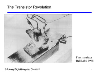
5. 5Lecture 5: IC Fabrication
Silicon IC processing
Similar to photographic printing
Expose the silicon wafer through a mask
Process the silicon wafer
Repeat sequentially to pattern all the layers
Layout: A set of masks that tell a fabricator what to
pattern
For each layer in your circuit
Layers are metal, drain/source implants, gate, etc.
You draw the layers
Subject to vendor-supplied spacing rules
6. 6Lecture 5: IC Fabrication
The wafer
Czochralski process
Melt silicon at 1425 °C
Add impurities (dopants)
Spin and pull crystal
Slice into wafers
0.25mm to 1.0mm thick
Polish one side
8. 8Lecture 5: IC Fabrication
Crystal and wafer
Wand
(a finished 250lb crystal)
A polished wafer
9. 9Lecture 5: IC Fabrication
4X reticle
Wafer
The mask
Illuminate reticle on wafer
Typically 4× reduction
Typical image is 25×25mm
Limited by focus
Step-and repeat across
wafer
Limited by mechanical
alignment
10. 10Lecture 5: IC Fabrication Reference: FULLMAN KINETICS
Lithography
Patterning is done by exposing photoresist with light
Requires many steps per “layer”
Example: Implant layer
22. 22Lecture 5: IC Fabrication
Detailed process sequence
1. Grow epi layer
Ultra-pure single-crystal
silicon
2. Implant n-well
23. 23Lecture 5: IC Fabrication
Detailed process sequence (con’t)
3. Define active area
4. Grow field oxide
For isolation
24. 24Lecture 5: IC Fabrication
Detailed process sequence (con’t)
5. Grow gate oxide
6. Pattern polysilicon
25. 25Lecture 5: IC Fabrication
Detailed process sequence (con’t)
7. Form pFETs
8. Form nFETs
26. 26Lecture 5: IC Fabrication
Detailed process sequence (con’t)
9. Deposit LTO by CVD
LTO is low-temperature
oxide
CVD is chemical vapor
deposition
10. Deposit Metal1
Usually aluminum
27. 27Lecture 5: IC Fabrication
Detailed process sequence (con’t)
11. Via definition
Deposit LTO
Make via cuts
12. Deposit Metal2
Usually aluminum
13. Overglass (not shown)
Coat entire chip with Si3N4
Make pad openings in Si3N4
40. 40Lecture 5: IC Fabrication
Projections
Simulated distribution of dopant
atoms in a 0.05m nFET
red: acceptor atom
blue: donor atom
All figures from IEEE Spectrum, 7/99
46. 46Lecture 5: IC Fabrication
Cost of Integrated Circuits
NRE (non-recurrent engineering) costs
design time and effort, mask generation
one-time cost factor
Recurrent costs
silicon processing, packaging, test
proportional to volume
proportional to chip area