0.49 inch Micro OLED 1920X1080 MIPI interface

Model: BO049FHPMO Small-size, high resolution 0.49"FHD Display .AP Operated Resolution 1920 ×1080 PPI=4496 .Frame ratesupports 50~100Hz .Normal operation supports full color mode , 16.7M colors .Fast response .Thin and light in weight .Color enhancement .High contrast .IR compensation with 2D .Idle mode for save power .Scan direction selection, up or down and right or left .Interface .Support MIPI only or MIPI+I2C .Support VESA-DSC in-chip decoder (3X and 3.75X compression ratio) .Support scaling up 1.33 X (1440 ×810 to 1920 ×1080) and 1.5 X (1280 ×720 to 1920 ×1080) and 2 X ( 960 ×540 to 1920 ×1080) .Sequential emission .Support 8bit/10bit input pattern format https://www.panoxdisplay.com/micro-display/0-49-inch-micro-oled-display-1920x1080-mipi-interface.html

Recommended
More Related Content
Similar to 0.49 inch Micro OLED 1920X1080 MIPI interface
Similar to 0.49 inch Micro OLED 1920X1080 MIPI interface (20)
Recently uploaded
Recently uploaded (20)
0.49 inch Micro OLED 1920X1080 MIPI interface
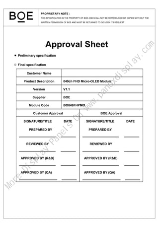
- 1. Approval Sheet ■ Preliminary specification □ Final specification Customer Approval BOE Approval SIGNATURE/TITLE DATE PREPARED BY REVIEWED BY APPROVED BY (R&D) APPROVED BY (QA) SIGNATURE/TITLE DATE PREPARED BY REVIEWED BY APPROVED BY (R&D) APPROVED BY (QA) Customer Name Product Description 049ch FHD Micro-OLED Module Version V1.1 Supplier BOE Module Code BO049FHPMO PROPRIETARY NOTE : THIS SPECIFICATION IS THE PROPERTY OF BOE AND SHALL NOT BE REPRODUCED OR COPIED WITHOUT THE WRITTEN PERMISSION OF BOE AND MUST BE RETURNED TO OE UPON ITS REQUEST M o r e D i s p l a y P a n e l s O n w w w . p a n o x d i s p l a y . c o m
- 2. I Confidential Contents Revision................................................................................................................................................................................................. III 1. Overview/Application ............................................................................................................................................................. 1 2. Features........................................................................................................................................................................................ 1 3. Module Structure...................................................................................................................................................................... 1 4. System Block Diagram............................................................................................................................................................ 2 4.1 Pin description............................................................................................................................................................. 3 4.2 Peripheral Circuit....................................................................................................................................................... 5 5. Interface....................................................................................................................................................................................... 6 5.1 I2C Interface ................................................................................................................................................................ 6 5.1.1 I2C-Bus Protocol................................................................................................................................................... 7 5.1.2 Write Sequence...................................................................................................................................................... 7 5.1.3 Read Sequence ....................................................................................................................................................... 7 5.2 MIPI Interface............................................................................................................................................................. 8 5.2.1 DSI System Configuration................................................................................................................................. 8 5.2.2 Multi-Lane Distribution and Merging........................................................................................................... 9 5.2.3 Interface Level Communication ....................................................................................................................10 5.2.4 Operation Modes.................................................................................................................................................10 5.2.5 High-Speed Data Transmission (HSDT) .....................................................................................................12 5.2.6 Burst of High-Speed Data Transmission.....................................................................................................12 5.2.7 Bi-directional Lane Turn around(BTA) ......................................................................................................13 5.2.8 Interface Level Communication ....................................................................................................................13 5.2.9 Peripheral-to-Processor LP Transmissions ................................................................................................17 5.3 Tearing Effect Output.............................................................................................................................................18 6. Absolute Maximum Ratings ...............................................................................................................................................19 7. Electrical Characteristics.....................................................................................................................................................20 7.1 DC Characteristics...................................................................................................................................................20 7.2 AC Characteristics...................................................................................................................................................20 7.2.1 MIPI High Speed Mode Characteristics.....................................................................................................20 7.2.2 MIPI Low Power Mode Characteristics .....................................................................................................20 7.2.3 MIPI Video Timing Specification..................................................................................................................21 7.2.4 I2C Interface Timing .........................................................................................................................................21 7.2.5 I2C Interface Waveform...................................................................................................................................22 7.3 Power Consumption.................................................................................................................................................22 8. Power Supply Sequence........................................................................................................................................................23 8.1 Power On/Off Sequence..........................................................................................................................................23 9. Description of Function........................................................................................................................................................24 9.1 Display Mode..............................................................................................................................................................24 9.1.1 Power Mode..........................................................................................................................................................24 9.1.2 Idle Mode...............................................................................................................................................................24 9.1.3 BIST Mode ............................................................................................................................................................24 9.1.4 Command Enable Mode...................................................................................................................................26 9.2 Display Active-Area(AA) Control .......................................................................................................................28 M o r e D i s p l a y P a n e l s O n w w w . p a n o x d i s p l a y . c o m
- 3. II Confidential 9.2.1 Resolution (80h CMD1) ....................................................................................................................................29 9.2.2 Active-Area (AA) control Column Address Set (2Ah CMD1)..............................................................30 9.2.3 Active-Area (AA) control Row Address Set (2Bh CMD1).....................................................................30 9.2.4 Active-Area (AA) control Pixel shift Set (B4h CMD1)...........................................................................31 9.3 Scan direction selection (36h CMD1).................................................................................................................33 9.4 Read Display Power Mode (0Ah CMD1)..........................................................................................................35 9.5 SCACTRL: Scaling up control (69h CMD1)...................................................................................................35 10. Optical Characteristics.........................................................................................................................................................36 10.1 Optical Characteristics...........................................................................................................................................36 10.2 Measurement System/Measurement Method..................................................................................................36 11. Reliability Rest ........................................................................................................................................................................37 12. Pixel Alignment .......................................................................................................................................................................38 13. Package Outline ......................................................................................................................................................................38 13.1 FPC Module(Unit : mm) ........................................................................................................................................38 14. Packing Information..............................................................................................................................................................39 14.1 Packing Description.................................................................................................................................................39 14.2 Packing Procedure....................................................................................................................................................39 14.3 Lable Information ....................................................................................................................................................40 14.3.1 MDL ID................................................................................................................................................................40 14.3.2 Serial No. Naming Rule..................................................................................................................................40 15. Recommended Items .............................................................................................................................................................41 15.1 Suppression of the Panel Temperature..............................................................................................................41 16. Notes on Handling..................................................................................................................................................................42 16.1 Static charge prevention.........................................................................................................................................42 16.2 Protection from dust and dirt...............................................................................................................................42 16.3 Others ...........................................................................................................................................................................42 M o r e D i s p l a y P a n e l s O n w w w . p a n o x d i s p l a y . c o m
- 4. III Confidential Revision Version Date Description V1.0 2022.04.20 Initial release V1.1 2022.07.15 Add Packing Information and Reliability Rest M o r e D i s p l a y P a n e l s O n w w w . p a n o x d i s p l a y . c o m
- 5. 1 Confidential 049 FHD Active Matrix Color OLED Panel Module 1. Overview/Application 2. BO049FHPMO is a 0.49 inch diagonal, FHD resolution (1920 × 1080), active matrix color OLED (Organic Light Emitting Display) panel module based on single crystal silicon backplane. The pixel circuits and driving IC are integrated on the silicon backplane to get the compact size and very low power consumption. Features Small-size, high resolution 0.49" FHD Display AP Operated Resolution 1920 ×1080 PPI=4496 Frame rate supports 50~100Hz Normal operation supports full color mode , 16.7M colors Fast response Thin and light in weight Color enhancement High contrast IR compensation with 2D Idle mode for save power Scan direction selection, up or down and right or left Interface Support MIPI only or MIPI+I2C Support VESA-DSC in-chip decoder (3X and 3.75X compression ratio) Support scaling up 1.33 X (1440 ×810 to 1920 ×1080) and 1.5 X (1280 ×720 to 1920 ×1080) and 2 X ( 960 ×540 to 1920 ×1080) Sequential emission Support 8bit/10bit input pattern format 3. Module Structure Active matrix color OLED display with on-chip driver based on single crystal silicon transistors M o r e D i s p l a y P a n e l s O n w w w . p a n o x d i s p l a y . c o m
- 6. 2 Confidential 4. System Block Diagram M o r e D i s p l a y P a n e l s O n w w w . p a n o x d i s p l a y . c o m
- 7. 3 Confidential 4.1 Pin description PIN No. (FPC Side) Symbol Type Description 1 ELVDD Output Power supply for OLED cell,Connect a capacitor for stabilization 2 VCOM Output Power supply for OLED cell,Connect a capacitor for stabilization 3 MVSS Power System GND for MIPI interface. 4 MVSS Power System GND for MIPI interface. 5 CLKN Input These pins are DSI-CLK- signals if MIPI Port interface is used. CLKP/N are differential small amplitude signals. If not used, please keep it open. 6 DATAP1 Input/ Output These pins are DSI-D1+ signals if MIPI Port interface is used. DATA1P/N are differential small amplitude signals. If not used, please keep it open. 7 CLKP Input These pins are DSI-CLK+ signals if MIPI Port interface is used. CLKP/N are differential small amplitude signals. If not used, please keep it open. 8 DATAN1 Input/ Output These pins are DSI-D1- signals if MIPI Port interface is used. DATA1P/N are differential small amplitude signals. If not used, please keep it open. 9 MVSS Power System GND for MIPI interface. 10 MVSS Power System GND for MIPI interface. M o r e D i s p l a y P a n e l s O n w w w . p a n o x d i s p l a y . c o m
- 8. 4 Confidential 11 DATAN0 Input/ Output These pins are DSI-D0- signals if MIPI Port interface is used. DATA0P/N are differential small amplitude signals. If not used, please keep it open. 12 DATAP2 Input/ Output These pins are DSI-D2+ signals if MIPI Port interface is used. DATA2P/N are differential small amplitude signals. If not used, please keep it open. 13 DATAP0 Input/ Output These pins are DSI-D0+ signals if MIPI Port interface is used. DATA0P/N are differential small amplitude signals. If not used, please keep it open. 14 DATAN2 Input/ Output These pins are DSI-D2- signals if MIPI Port interface is used. DATA2P/N are differential small amplitude signals. If not used, please keep it open. 15 MVSS Power System GND for MIPI interface. 16 VSS Power System GND for Internal digital system 17 DATAN3 Input/ Output These pins are DSI-D3- signals if MIPI Port interface is used. DATA3P/N are differential small amplitude signals. If not used, please keep it open. 18 VREF1 Power Regulator output for internal reference voltage. Connect a capacitor for stabilization. 19 DATAP3 Input/ Output These pins are DSI-D3+ signals if MIPI Port interface is used. DATA3P/N are differential small amplitude signals. If not used, please keep it open. 20 VGSP Output Gamma top voltage,Connect a capacitor for stabilization 21 VSS Power System GND for Internal digital system 22 VGMP Output Gamma top voltage,Connect a capacitor for stabilization 23 MVDD Output Regulator output for MIPI analog system power Connect a capacitor for stabilization. 24 VREF3 Output Regulator output for internal reference voltage. Connect a capacitor for stabilization. Connect a Schottky diode to GND 25 EN_AOI Input AOI mode enable. EN_AOI =0, AOI mode disable, EN_AOI =1, AOI mode enable 26 VREF2 Output Regulator output for internal reference voltage. Connect a capacitor for stabilization. 27 IM [0] Input Use to select the Interface type. IM [0] Command Execute Image Write 0 MIPI MIPI 1 I2C MIPI 28 SDA Input / Output Bi-direction data PIN in I2C I/F. If this pin is not used, please connect to VDDI. 29 RESX Input This signal will reset the device and must be applied to properly initialize the chip. Signal is active low. 30 SCL_WRX Input Synchronous clock signal in I2C I/F. If this pin is not used, please connect to VDDI. M o r e D i s p l a y P a n e l s O n w w w . p a n o x d i s p l a y . c o m
- 9. 5 Confidential 31 RL_SEL Input Use to select right/left-eye module.(It is recommended to connect to “0”) RL_SEL Right/Left Eye Module 0 Left-Eye 1 Right-Eye RL_SEL. 0 :salve address 0x4C or 0x4E ; RL_SEL. 1 :salve address 0x4D or 0x4E 32 OCP_OUT Output Over current protect output flag 33 V_TEST Power Connect to VCOM 34 GPIO Input / Output Digital global purpose in/out test pin. 35 OCP_VDD2 Output Regulator output for MIPI analog system power Connect a capacitor for stabilization. 36 EN_EXT_VDD Input Enable signal for external VDD power mode EN_EXT_VDD = 0 : internal VDD, EN_EXT_VDD = 1: external VDD 37 OTP_PWR Input OTP program power;If not use, please connect to GND or OPEN 38 AVSS Power System GND for analog system 39 AVEE Power -4.0V~6.5VPower supply for OLED cell. Connect a capacitor for stabilization 40 AVDD Power 5V~6.5VPower supply for analog system. Connect a capacitor for stabilization P1 VDDI Power Power supply for interface system except for MIPI interface. P2 VDD Power Regulator output for logic system power. Connector a capacitor for stabilization. 4.2 Peripheral Circuit Mounting the capacitor for each power supply to ensure that the panel display normally. M o r e D i s p l a y P a n e l s O n w w w . p a n o x d i s p l a y . c o m
- 10. 6 Confidential Notes: No. Signal Name Typical Value Maximum Rated Voltage Note 1 VDDI Cap, 2.2uF 6.3V 2 AVDD Cap, 1.0uF 10V 3 ELVDD Cap, 2.2uF 10V 4 AVEE Cap, 1.0uF 10V 5 VDD Cap, 4.7uF 6.3V 6 MVDD Cap, 1uF 6.3V 7 OTP_VDD2 Cap, 1uF 6.3V 8 VGMP Cap, 1uF 10V 9 VGSP Cap, 1uF 10V 10 VREF1 Cap, 1uF 6.3V 11 VREF2 Cap, 1uF 6.3V 12 VREF3 Cap, 1uF Schottky 6.3V 13 VCOM Cap, 2.2uF TVS 10V (1) There are totally 13 capacitors, 1 Schottky diode and 1 TVS. (2) The Schottky diode is placed between VREF3 and ground. (3) The TVS is placed between VCOM and ground. 5. Interface 0.49" Micro OLED supports MIPI interface and inter-integrated circuit interface (I2C). MIPI or I2C is selected by IM0, the detail interface selection by IM0 pin and shows in below table. IM0 Command Execute Image Write 0 MIPI MIPI 1 I2C MIPI 5.1 I2C Interface The I2C-bus is for bi-directional, two-line communication between different ICs or modules. The two lines are the Serial Data Line (I2C_SDA) and Serial Clock Line (I2C_SCL). Both lines must be connected to a positive power supply via pull-up resistors. Data transfer can be initiated only when the bus is not busy. The acknowledge takes place after every byte. The acknowledge bit allows the receiver to signal the transmitter that the byte was successfully received and another byte may be sent. The master generates all clock pulses, including the acknowledge ninth clock pulse. M o r e D i s p l a y P a n e l s O n w w w . p a n o x d i s p l a y . c o m
- 11. 7 Confidential 5.1.1 I2C-Bus Protocol Before any data is transmitted on the I2C-bus, the device which should response is addressed first. There are several slave addresses can be selected by MCU. The slave addressing is always carried out with the first byte transmitted after the START procedure. Definition -Transmitter: The device which sends the data to the bus. -Receiver: The device which receives the data from the bus. -Master: The device which initiates a transfer, generates clock signals and terminates a transfer. -Slave: The device addressed by a master. -Multi-master: More than one master can attempt to control the bus at the same time without corrupting the message. -Arbitration: Procedure to ensure that. If more than one master simultaneously tries to control the bus, only one is allowed to do so and the message is not corrupted. -Synchronization: Procedure to synchronize the clock signals of two or more devices. 5.1.2 Write Sequence 0.49" Micro OLED supports register write sequence via I2C-bus transfer. The register writing supports single register write mode. The detailed transfer sequences are illustrated and described as below. (1) Data transfer for register writing should follow the format shown as below. (2)After the START condition, a slave address is sent. R/W ̅ bit is setting to “0” for Write. (3)The slave issues an ACK to the master. (4)8-bits register address transfer first then transfer the register data parameter. (5)A data transfer is always terminated by a STOP condition. (6) The chip SA [6:0] =100_1100. 5.1.3 Read Sequence 0.49" Micro OLED supports register read sequence via I2C-bus transfer. The register reading supports single register read mode. The register data reading transfer are shown as below. M o r e D i s p l a y P a n e l s O n w w w . p a n o x d i s p l a y . c o m
- 12. 8 Confidential 5.2 MIPI Interface Display serial interface (DSI) specifies the interface between a host processor and a peripheral such as a display module. It builds on existing MIPI Alliance specification by adoption pixel formats and command set. The detail Lane configuration for DPHY is listed below. There are one Clock Lane and 1~4 Data Lane. The configuration for DPHY between host and 0.49" Micro OLED shows as the table below. Lane Pair Available Operation Mode Clock Lane Unidirectional Lane Forward High-Speed Clock Escape Mode (ULPS only) Data Lane 0 Bi-directional Lane Forward High-Speed Data Bi-directional Escape Mode Bi-directional LPDT Data Lane 1 Unidirectional Lane Forward High-Speed Data No LPDT Escape Mode (ULPM only) Data Lane 2 Unidirectional Lane Forward High-Speed Data No LPDT Escape Mode (ULPM only) Data Lane 3 Unidirectional Lane Forward High-Speed Data No LPDT Escape Mode (ULPM only) 5.2.1 DSI System Configuration 0.49" Micro OLED supports MIPI 1 port with 2, 3 or 4 lane configurations for DPHY. The system configuration is shown as the figure below. There are HW pin (IM) and registers (Lane_num_cfg, PSWAP, DSWAP) which can set the interface and lane related configuration for port. M o r e D i s p l a y P a n e l s O n w w w . p a n o x d i s p l a y . c o m
- 13. 9 Confidential 5.2.2 Multi-Lane Distribution and Merging DSI is a lane-scalable interface. Multi-lane implementations shall use a single common clock signal, shared by all data lane. In the transmitter, there will be a layer to distribute a sequence of packet bytes across N Lanes. And in the receiver, there will be a layer to merge this sequence of packet byte back to correct order. The data processing flow is shown as the figure below for DPHY one-lane/four-lane condition. M o r e D i s p l a y P a n e l s O n w w w . p a n o x d i s p l a y . c o m
- 14. 10 Confidential 5.2.3 Interface Level Communication DSI uses data and clock lane for DPHY communication. The Lane state is determined by driving certain Line levels. During normal operation, either a HS-TX or a LP-TX is driving a Lane. The HS-TX always drives the Lane differentially. The LP-TX drives two Lines for a Lane independently and single ended. These results of High-Speed Lane states and Low-Power Lane states for DPHY are as the table below. 5.2.4 Operation Modes During normal operation a Lane will be either in Control or High-Speed mode. The clock lane can be driven into three different modes: Low-Power Mode (LPM), Ultra-Low-Power Mode (ULPM) or High-Speed Clock Mode(HSCM). The Data Lane can be driven into following different modes: Escape Mode, HS Data Transmission, Bi-directional Data Lane Turnaround (BTA). The entry and leaving protocol flow chart for DPHY are as below. 5.2.4.1 Escape Modes Escape mode is a special mode of operation for Data Lanes using Low-Power stated. With this mode some additional functionality becomes available. Adata Lane shall enter Escape mode via Escape mode Entry procedure: LP-11→LP- 10→LP-00→LP-01→LP-00. An 8-bit entry command shall be sent to indicate the requested action. The available Escape mode commands and actions are as the table below. Escape Command Command Type Entry Command Pattern M o r e D i s p l a y P a n e l s O n w w w . p a n o x d i s p l a y . c o m
- 15. 11 Confidential (First bit → Last bit) Low-Power Data Transmission Mode 1110 0001 Ultra-Low Power State Mode 0001 1110 Undefined mode Mode 1001 1111 Undefined mode Mode 1101 1110 Remote Application Reset Trigger 0110 0010 Tearing Effect Trigger 0101 1101 Acknowledge Trigger 0010 0001 Unknown Trigger 1010 0000 5.2.4.2 Low Power Data Transmission If the Escape mode Entry procedure is followed up by Entry Command for Low Power Data Transmission (LPDT). Data can be communicated by the protocol at low speed. The LPDT waveform is as follows and the figure below. Escape mode Entry Sequence: LP-11→LP-10→LP-00→LP-01→LP-00. Escape Entry Command(87h) for LPDT LP data for LPDT Mark-1 (LP-00→LP-10→LP-11)to leave Escape mode Ultra-Low-Power State The MCU can force data lane in Ultra-Low-Power State(ULPS) by Escape Mode with ULPS Entry Command. The sequence to force data lane in ULPS is as follows and the figure below. Escape mode Entry Sequence: LP-11→LP-10→LP-00→LP-01→LP-00. Escape Entry Command(78h) for ULPS Mark-1 (LP-00→LP-10→LP-11)to leave Escape mode LP-11 LP10 LP-00 LP-01 LP-00 0 0 LP-00 LP10 LP-11 M o r e D i s p l a y P a n e l s O n w w w . p a n o x d i s p l a y . c o m
- 16. 12 Confidential 5.2.5 High-Speed Data Transmission (HSDT) For High-Speed Data Transmission in DPHY, Clock lane have to enter High-Speed Clock Mode (HSCM) before Data lanes enter High-Speed Data Transmission. And the Data lanes have to leave High-Speed Data Transmission after Clock lanes already left HSCM. The High-Speed Data Transmission sequence for DPHY is as the figure below. ■ Data Lane 1. HS request sequence: LP-11 → LP-01 → LP-00 2. Keep HS-0 for certain time 3. Start of Transmission sequence (B8h) 4. HS data for HSDT 5. End of Transmission sequence (HS-0 if last data bit is HS-1, HS-1 if last data bit is HS-0) 6. Back to LP-11 to leave HSDT ■ Clock Lane 1. HS request sequence: LP-11 → LP-01 → LP-00 2. Keep HS-0 for certain time 3. High speed clock mode 4. Keep HS-0 for certain time 5. Back to LP-11 to leave HSCM 5.2.6 Burst of High-Speed Data Transmission For HSDT, there can be one data packet or multiple packets in one HS burst. These data packets can be long packet (LPa) or Short packet (SPa). HSDT with End of Transmission Packet(EoTP) or without it is selectable. examples are as below. M o r e D i s p l a y P a n e l s O n w w w . p a n o x d i s p l a y . c o m
- 17. 13 Confidential 5.2.7 Bi-directional Lane Turn around(BTA) The transmission direction of a bi-directional lane can be swapped by means of a turnaround procedure. The procedure enable information transfer in the opposite direction and this procedure is the same for either a change from forward-to-reverse or reverse-to-forward direction. The BTA procedure is as follows and the figure below. 1. MCU send Turnaround Request sequence: LP-11→LP-10→LP-00→LP-10→LP-00 2. MCU change to Hi-Z state and wait for display module start to control the D0 Lane 3. Display module control the Lane and change to stop state: LP-00→LP-10→LP-11 5.2.8 Interface Level Communication There are two packet structures are defined for communication: Short Packets(SPa) and Long Packets(LPa). For both packet structures, the Data Identifier(DI) is always the first bit of the packet. 5.2.8.1 General Packet Structure For DPHY, Short Packets are four bytes in length including 1 byte DI, 2 bytes data or command and 1 byte Error Correction Code(ECC). The ECC byte is used to check if the first 3 bytes in Packet Header (DI and data) is correct or not. And the ECC byte allows single-bit error to be corrected and 2- bit errors to be detected. The packet format for Short Packets are illustrated as the following. As to Long Packets, they shall consist of three elements: 4 bytes Packet Header, Data Payload with a variable number of bytes and 2 bytes Packet Footer. The Packet Header includes 1 byte DI, 2 bytes Word Count(WC) and 1 byte ECC. The Word Count in Packet Header will decide the number of total bytes of the Data Payload. The Packet Footer has 2 bytes Checksum used to check if the Payload Data is correct or not. The packet format for Long Packets are illustrated as the following. M o r e D i s p l a y P a n e l s O n w w w . p a n o x d i s p l a y . c o m
- 18. 14 Confidential 5.2.8.2 Bit Order and Byte Order for Packets The bit order for packets is the Least Signification Bit sent first and the Most Significant Bit sent last. And for the byte order for packets is the Least Signification Byte sent first and the Most Significant Byte sent last. 5.2.8.3 Common Packet Elements There are several common elements for Long and Short Packets such as DI byte and ECC byte. The DI byte consists of 2-bit Virtual Channel identifier (VC = DI[7:6]) and 6-bit Data Type field (DT = DI[5:0]). The DI structure is as the following. Data Identifier(DI) VirtualChannel(VC) DataType(DT) Bit-7 Bit-6 Bit-5 Bit-4 Bit-3 Bit-2 Bit-1 Bit-0 Virtual Channel is used to assign which peripherals for packets transmission. Data Type specifies if the packet is a Long or Short Packet and the packet format. The Data Type are defined as the table below. Data Types for Peripheral-Sourced Packets Data Type(hex) Data Type(binary) Description Packet Size 0x02 00 0010 Acknowledge and Error Report Short 0x11 01 0001 Generic Short READ Response, 1 byte returned Short 0x12 01 0010 Generic Short READ Response, 2 bytes returned Short 0x1A 01 1010 Generic Long READ Response Long 0x1C 01 1100 DCS Long READ Response Long 0x21 10 0001 DCS Short READ Response, 1 byte returned Short 0x22 10 0010 DCS Short READ Response, 2 bytes returned Short Data Types for Processor-Sourced Packets Data Type(hex) Data Type(binary) Description Packet Size 0x01 00 0001 Sync Event, V Sync Start Short 0x11 01 0001 Sync Event, V Sync End Short 0x21 10 0001 Sync Event, H Sync Start Short M o r e D i s p l a y P a n e l s O n w w w . p a n o x d i s p l a y . c o m
- 19. 15 Confidential 0x31 11 0001 Sync Event, H Sync End Short 0x07 00 0111 Compression Mode Command Short 0x08 00 1000 End of Transmission packet (EoTp) Short 0x03 00 0011 Generic Short WRITE, no parameters Short 0x13 01 0011 Generic Short WRITE, 1 parameter Short 0x23 10 0011 Generic Short WRITE, 2 parameters Short 0x04 00 0100 Generic READ, no parameters Short 0x14 01 0100 Generic READ, 1 parameter Short 0x24 10 0100 Generic READ, 2 parameters Short 0x05 00 0101 DCS Short WRITE, no parameters Short 0x15 01 0101 DCS Short WRITE, 1 parameter Short 0x06 00 0110 DCS READ, no parameters Short 0x37 11 0111 Set Maximum Return Packet Size Short 0x09 00 1001 Null Packet, no data Long 0x19 01 1001 Blanking Packet, no data Long 0x29 10 1001 Generic Long Write Long 0x39 11 1001 DCS Long Write Long 0x0A 00 1010 Picture Parameter Set Long 0x0B 00 1011 Compressed Pixel Stream Long 0x0E 00 1110 Packed Pixel Stream, 16-bit RGB, 5-6-5 Format Long 0x1E 01 1110 Packed Pixel Stream, 18-bit RGB, 6-6-6 Format Long 0x2E 10 1110 Loosely Packed Pixel Stream, 18-bit RGB, 6-6-6Format Long 0x3E 11 1110 Packed Pixel Stream, 24-bit RGB, 8-8-8 Format Long As to ECC, the host processor shall always calculate and transmit an ECC byte to identify the error for the Packet Header. The bits of ECC are defined as the rule below. The symbol ‘^’ means XOR function. P7 and P6 are set to 0 because Error Correction Code is based on 64-bit value but this ECC implementation is only used for 24-bit value. P7 = 0 P6 = 0 P5 = D10^D11^D12^D13^D14^D15^D16^D17^D18^D19^D21^D22^D23 P4 = D4^D5^D6^D7^D8^D9^D16^D17^D18^D19^D20^D22^D23 P3 = D1^D2^D3^D7^D8^D9^D13^D14^D15^D19^D20^D21^D23 P2 = D0^D2^D3^D5^D6^D9^D11^D12^D15^D18^D20^D21^D22 P1 = D0^D1^D3^D4^D6^D8^D10^D12^D14^D17^D20^D21^D22^D23 P0 = D0^D1^D2^D4^D5^D7^D10^D11^D13^D16^D20^D21^D22^D23 M o r e D i s p l a y P a n e l s O n w w w . p a n o x d i s p l a y . c o m
- 20. 16 Confidential 5.2.8.4 Packet Footer for Long Packets The Packet Footer for Long Packets is a checksum value which is calculated from the Data Payload in the Long Packet. The checksum is using a 16-bit Cyclic Redundancy Check(CRC) with a generator polynomial of x^16 + x^12 + x^5 + x^0. The Receiver will calculate checksum value from received Data Payload and compare this CRC value with the Packet Footer sent by transmitter. If calculated CRC values equal to Packet Footer, the received Data Payload are correct. The CRC implementation is presented as the following. 5.2.8.5 Packet Pixel Stream Format There are 4 packet pixel stream format: 16-bit RGB 5-6-5, 18-bit RGB 6-6-6, loosely packed 18- bit RGB 6-6-6 and 24-bit RGB 8-8-8. The Data Type for these pixel stream format are shown as the table below. Note: 0.49" Micro OLED only support 24-bit RGB pixel stream format 5.2.8.6 16- bit RGB Format, Data Type = 0x0E The data of 16-bit RGB pixel format comprise of five bits red, six bits green and five bits blue. Note that the “Green” component is split across two bytes. The pixel stream format is shown as the figure below. 5.2.8.7 18- bit RGB Format, Data Type = 0x1E The data of 18-bit RGB pixel format comprise of six bits red, six bits green and six bits blue. The pixel stream format is shown as the figure below. Data Type(hex) Data Type(binary) Description Packet Size 0x0E 00 1110 Packed Pixel Stream, 16-bit RGB, 5-6-5 Format Long 0x1E 01 1110 Packed Pixel Stream, 18-bit RGB, 6-6-6 Format Long 0x2E 10 1110 Loosely Packed Pixel Stream, 18-bit RGB, 6-6-6 Format Long 0x3E 11 1110 Packed Pixel Stream, 24-bit RGB, 8-8-8 Format Long M o r e D i s p l a y P a n e l s O n w w w . p a n o x d i s p l a y . c o m
- 21. 17 Confidential 5.2.8.8 18-bit Loosely RGB Format, Data Type = 0x2E The data of 18-bit loosely RGB pixel format comprise of six bits red, six bits green and six bits blue. But the six bits of each color is shifted to the upper bits of the byte and the bit[1:0] of each payload byte are ignored. This requires more bandwidth than the “packed” format but requires less shifting and multiplexing logic in the packing and unpacking function. The pixel stream format is shown as the figure below. 5.2.8.9 24-bit RGB Format, Data Type = 0x3E The data of 24-bit RGB pixel format comprise of eight bits red, eight bits green and eight bits blue. The pixel stream format is shown as the figure below. 5.2.9 Peripheral-to-Processor LP Transmissions All systems require bi-directional capability for returning READ data, acknowledge or error information to the Host Processor. It shall use Lane 0 for all peripheral-to-processor transmissions. Reverse-direction signaling shall only use Low Power mode of Transmission. Packet structure for peripheral-to-processor transactions is the same as for the processor-to-peripheral direction. There are four basic types for peripheral-to-processor transactions: Acknowledge, Acknowledge and Error Report, Response to Read Request, Tearing Effect(TE) Acknowledge and Error Report is a Short Packet sent if any errors were detected in preceding transmissions from the Host Processor. Once the Errors are reported, the accumulated errors in the error register are cleared. An error report is a short packet comprised of two bytes following the DI byte and with an ECC byte following the Error Report bytes. Detection and reporting of each error types is signified by setting the corresponding bit to “1”. The bit assignment for all error reporting is shown as the table below. Bit Description 0 SoT Error 1 SoT Sync Error 2 EoT Sync Error 3 Escape Mode Entry Command Error 4 Low-Power Transmit Sync Error 5 Peripheral Timeout Error 6 False Control Error 7 Contention Detected 8 ECC Error, singl-bit(detected and corrected) 9 ECC Error, multi-bit(detected, not corrected) M o r e D i s p l a y P a n e l s O n w w w . p a n o x d i s p l a y . c o m
- 22. 18 Confidential 10 Payload Checksum Error 11 DSI Data Type Not Recognized 12 DSI VC ID Invalid 13 Invalid Transmission Length 14 Reserved 15 DSI Protocol Violation 5.3 Tearing Effect Output The tearing effect (TE) output signal used to be a synchronization signal for command mode display application. A command mode display has its own timing control and memory frame buffer. To avoid tearing effect, it is needed to synchronize timing between host and panel. There are three kinds of TE mode supported from display module. These TE output signals can be enable, disable and select by DCS command 35h, 34h and 44h. In below shows the different TE output mode: TE Mode1: The tearing effect output signal consists of V-Blanking only. tvdh = display data is not updated and counted by line base. The duration is “VFP+VBP-1” lines. tvdl = display data is updated and counted by line base. The duration is “Display Y-direction number+1” lines. TE Mode2: The tearing effect output signal consists of V-Blanking and H-Blanking. thdh = display data is not updated and counted by pixel clock base.(H-Blanking) thdl = display data is updated and counted by pixel clock base. TE Mode3: The tearing effect output signal consists of V-Blanking and H-Blanking N = the N-th line after V-blanking, which is set by 44h command. Mode selection for TE output Mode selection for TE outpuN (35h), TEOFF (34h) TEON (35h]), M(bit0) STESL (44h), N[15:0] TE Output TEOFF X X TE off (output low) M o r e D i s p l a y P a n e l s O n w w w . p a n o x d i s p l a y . c o m
- 23. 19 Confidential TEON M =0 N[15:0] = 0 TE mode1 TEON M =1 N[15:0] = 0 TE mode2 TEON M =0 N[15:0] ≠ 0 TE mode3 Parameter Description Min Typ. Max Unit tvdh Vertical Timing High Duration 319 - - us tvdl Vertical Timing Low Duration 11.11 - - ms thdh Horizontal Timing High Duration - - 0.3 us thdl Horizontal Timing Low Duration 9.64 - - us Note: resolution is 1920x1080 under frame rate 90Hz, driver IC operates in sequential mode with VFP=VBP=16. 6. Absolute Maximum Ratings The absolute maximum rating is listed on the below table. When the display product is used beyond the absolute maximum ratings, it may be permanently damaged. It is strongly recommended use the driver IC within the following specified limits for normal operation. If these electrical characteristic conditions are exceeded during normal operation, the driver IC will malfunction and causepoor reliability. Item Symbol Value Unit Power Supply Voltage (1) VDDI 2 V Power Supply Voltage (2) AVDD-AVSS 5.7 V AVEE-AVSS -6.2 V MIPI Differential Input CLKP, CLKN, DATAP0, DATAN0 DATAP1, DATAN1 DATAP2, DATAN2 DATAP3, DATAN3 1.32 V Input Voltage of Interface Vin -0.3 ~ VDDI+0.3 V Output Voltage of Interface Vo -0.3 ~ VDDI+0.3 V Operating temperature Topr -20 ~ 60 ° C Storage temperature Tstg -30 ~ 80 ° C Note : The environment temperature is not a RA test temperature. M o r e D i s p l a y P a n e l s O n w w w . p a n o x d i s p l a y . c o m
- 24. 20 Confidential 7. Electrical Characteristics 7.1 DC Characteristics Parameter Symbol Condition Min. Typ. Max. Unit Power & Operation Voltage/Current AVDD Input Level AVDD Voltage - 5.4 5.5 5.6 V AVDD Input Current - - - 100 mA AVEE Input Level AVEE Voltage - -6.1 -6.0 -5.9 V AVEE Input Current - - - 100 mA VDDI Input Level VDDI Voltage - 1.65 1.8 1.95 V VDDI Input Current - - - 100 mA MIPI I/O Power Supply MVDD - - 1.26 - V Note:Typical voltage is required necessarily for best display performance. 7.2 AC Characteristics 7.2.1 MIPI High Speed Mode Characteristics Parameter Symbol Min Typ. Max Unit UI instantaneous UIINST 1 - 3 ns T Data to Clock Skew TSKEW -0.15 - 0.15 UIHS RX Data to Clock Setup Time Tolerance TSETUP 0.15 - - UIHS RX Data to Clock Hold Time Tolerance THOLD 0.15 - - UIHS 1 UIINST 1 Clock Period TSETUP THOLD 0.5UIINST+TSKEW CLKP CLKN 7.2.2 MIPI Low Power Mode Characteristics Parameter Description Min Typ. Max Unit TLPX(M) Transmitted length of any Low-Power state period (MCU to display module) 50 - - ns TLPX(D) Transmitted length of any Low-Power state period (display module to MCU) 50 - - ns TTA-SURE Time that the new transmitter waits after the LP-10 state before transmitting the Bridge state(LP-00) during a Link TLPX - 2*TLPX M o r e D i s p l a y P a n e l s O n w w w . p a n o x d i s p l a y . c o m
- 25. 21 Confidential Turnaround TTA-GET Time that the new transmitter drives the Bridge state(LP-00) after accepting control during a Link Turnaround 5*TLPX TTA-GO Time that the transmitter drives the Bridge state(LP-00) before releasing control during a Link Turnaround 4*TLPX 7.2.3 MIPI Video Timing Specification ※This parameter is a typical example illustrating the display timing. BOE cannot assume responsibility for any problems arising out of the use of the circuit. 7.2.4 I2C Interface Timing Parameter Symbol Min. Typ. Max. Unit I2C Clock Frequency Fclk - - 400 kHz I2C Clock Low Tclkl 1300 - - ns I2C Clock High Tclkh 600 - - ns I2C Data Rising Time Tdr - - 300 ns I2C Data Falling Time Tdf - - 300 ns I2C Data Setup Time Tdsu 100 - - ns I2C Data Hold Time Tdhd - - TBD ns I2C Setup Time (Start Condition) Tsu_sta 600 - - ns 1920× 1080@60Hz H Hsync 4 V Vsync 2 HBP 60 VBP 14 Hactive 1920 Vactive 1080 HFP 88 VFP 16 Recommended configuration of MIPI D-PHY V1.2 DSI 1.01 CLK Mode: Discontinue Mode MIPI Lane: 4 Lanes@60Hz Video Mode: Burst Mode HS Speed: 300Mbps ~ 1.0Gbps per Lane LP Speed: 10Mbps(max) General Packet Structure:DCS Mode .Data Type of Packet:0x39 or 0x05 or 0x15 M o r e D i s p l a y P a n e l s O n w w w . p a n o x d i s p l a y . c o m
- 26. 22 Confidential I2C Hold Time (Start Condition) Thd_sta 600 - - ns I2C Setup Time (Stop Condition) Tsu_stp 600 - - ns I2C Bus Free Time (Stop Condition) Tbuf_stp 1300 - - ns Notes: No. ITEM Description Note 1 Slave address 0x4C 2 Pull-up resistor 4.7KΩ@100Kbps 3 Read bit Setting “1” for write 4 Write bit Setting “0” for write 5 Start condition SDA is setting from “1” to “0” when SCL is “1” 6 Stop condition SDA is setting from “0” to “1” when SCL is “1” 7.2.5 I2C Interface Waveform SADD [6] W/R ACK 0 SCL_WRX SDA ACK ACK ACK ACK SADD [5] SADD [4] SADD [3] SADD [2] SADD [1] SADD [0] RADD [8] RADD [9] RADD [10] RADD [11] RADD [12] RADD [13] RADD [14] RADD [15] RADD [7] RADD [6] RADD [5] RADD [4] RADD [3] RADD [2] RADD [1] RADD [0] 0 0 0 0 0 0 0 DATA [7] DATA [6] DATA [5] DATA [4] DATA [3] DATA [2] DATA [1] DATA [0] Start Stop SADD[6:0]—Slave address. W—Write bit. R—Read bit. W=0. R=1. ACK—Acknowledge bit. ACK=0. RADD[15:0]—Register address. RADD[7:0] is for shifting. DATA[7:0]—The parameter of register. Code Example: MIPI format: regw 0x51 0xFF 0x01 I2C format: regw 0x51 0x00 0x00 0xFF regw 0x51 0x01 0x00 0x01 7.3 Power Consumption Symbol Condition Max. Unit 700cd/m2 consumption power - Tpnl = 25° C 60Hz 260 mW Note: All white raster display, frame rate=60Hz, resolution= 1920×1080. M o r e D i s p l a y P a n e l s O n w w w . p a n o x d i s p l a y . c o m
- 27. 23 Confidential 8. Power Supply Sequence 8.1 Power On/Off Sequence Power on sequence For FPC Module T1 100% V DDI 0% T3 T4 Initial code Sleep out unknown Reset MTP Reload Command Input Power on sequence Display off 100% A VDD 0% T5 Display on Display on IC State VDDI AVDD RESX MIPI I/F Image write LP-11 100% A VE E 0% AVEE T2 T6 Power off sequence For FPC Module Display off T7 IC State VDDI AVDD RESX MIPI I/F AVEE T8 Display on Display off Power off sequence RESET unknown Sleep in T9 T10 T11 Symbol Min. Typ. Max. Unit Description T1 1 - - ms Power on time between AVDD(VIN) and VDDI T2 1 - - ms Power on time between AVDD and AVEE. AVDD cannot be later than AVEE T3 1 - - ms Effective hardware reset period T4 20 - - ms MTP reload time T5 0 - - ms The time is between initial code finished and sleep-out command T6 2 - 8 VS Power on sequence, the period can be modified T7 1 - - VS Blanking region T8 - 1 - VS Power off sequence, the period can be modified T9 0 - - ms Power off time between AVEE and AVDD. AVDD cannot be earlier than AVEE T10 1 - - ms Effective hardware reset period T11 1 - - ms Power off time between AVDD(VIN) and VDDI M o r e D i s p l a y P a n e l s O n w w w . p a n o x d i s p l a y . c o m
- 28. 24 Confidential 9. Description of Function 9.1 Display Mode 9.1.1 Power Mode ITEM Code value Sleep In 0x10 Sleep Out 0x11 Display On 0x29 Display Off 0x28 9.1.2 Idle Mode ITEM Code value Idle On 0x39(Default value) Idle Off 0x38 9.1.3 BIST Mode BIST On/Off Control (C4h) Instruction R/W Address name Parameter MIPI Other D15- D8 D7 D6 D5 D4 D3 D2 D1 D0 BISTONOF F R/W C4h C400h - 1 0 1 0 0 1 0 1 C401h - 0 1 0 1 0 1 0 1 C402h - - - - - - - - BION 1 C403h - BION 2 - - - - - - - Description This command is used to control BIST function (Free Run mode). BIST function enable step: Enter Sleep-In(10h) mode. Setting PATENICYC[1:0] and BISTPATEN[11:0] to control the display cycle time and pattern. Setting BION1=”1” and BION2=”1”, the driver IC will start to run the BIST function. BIST function disable step: Setting BION1=”0” and BION2=”0”,the driver IC will return to normal function. Sending MIPI video data and enter Sleep-Out(11h) mode for normal display. Restriction - M o r e D i s p l a y P a n e l s O n w w w . p a n o x d i s p l a y . c o m
- 29. 25 Confidential Default Status Default Value Power On Sequence C400h AAh C401h 55h C402h 00h C403h 00h BIST CTRL (C5h) Instruction R/W Address name Parameter MIPI I2C D15- D8 D7 D6 D5 D4 D3 D2 D1 D0 BISTSET R/W C5h C500h - - PATENICYC[2:0] BISTPATEN[11:8] C501h - BISTPATEN[7:0] C502h - GRAY_LEVEL[7:0] C503h - R_LEVEL[7:0] C504h - G_LEVEL[7:0] C505h - B_LEVEL[7:0] Description This command is used to set the display pattern in BIST function. PATENICYC[1:0] : Cycle time between each display pattern. PATENICYC[1:0] Pattern cycle time 0h 256 Frame 1h 512 Frame 2h 1024 Frame 3h 2048 Frame BISTPATEN[11:0] : Select the display pattern in BIST function. BISTPATEN[9:0] Description BISTPATEN[0] Red pattern. ( by GRAY_LEVEL[7:0]) BISTPATEN[1] Green pattern. ( by GRAY_LEVEL[7:0]) BISTPATEN[2] Blue pattern. ( by GRAY_LEVEL[7:0]) BISTPATEN[3] Black pattern. BISTPATEN[4] Gray Level pattern. ( by R/G/ B_LEVEL[7:0]) BISTPATEN[5] Vertical Gradation pattern. BISTPATEN[6] Horizontal Gradation pattern. BISTPATEN[7] Color Bar pattern. BISTPATEN[8] Crosstalk with boundary pattern. Others Reserved Note1: the patterns which the bit number of BISTPATEN[9:0] is set to “1” will display and change automatically. Note2: When BISTPATEN[11:0]=12’h000, display pattern will be black pattern. GRAY_LEVEL[7:0] : Set the gray level when BISTPATEN[4]=”1” in BIST function. GRAY_LEVEL[7:0] Description 0h Gray Level : 00h 1h Gray Level : 01h 2h Gray Level : 02h M o r e D i s p l a y P a n e l s O n w w w . p a n o x d i s p l a y . c o m
- 30. 26 Confidential : : FDh Gray Level : FDh FEh Gray Level : FEh FFh Gray Level : FFh R_LEVEL[7:0] / G_LEVEL[7:0] / B_LEVEL[7:0] : Set the R/G/B level when BISTPATEN[4]=”1” in BIST function. GRAY_LEVEL[7:0] Description 0h R/G/B Gray Level : 00h 1h R/G/B Gray Level : 01h 2h R/G/B Gray Level : 02h : : FDh R/G/B Gray Level : FDh FEh R/G/B Gray Level : FEh FFh R/G/B Gray Level : FFh Restriction - Default Status Default Value Power On Sequence C500h 00h C501h 08h C502h FFh C503h FFh C504h FFh C505h FFh 9.1.4 Command Enable Mode F000H MAUCCTR Instruction R/W Address Parameter MIPI Other D15- D8 D7 D6 D5 D4 D3 D2 D1 D0 MAUCCTR W F0h F000h - 1 0 1 0 1 0 1 0 F001h - - - - D4 D[3:0] Description This command is used to enable the access of CMD2 page. Bit Symbol Description Comment D4 EN_CMD2 Enable access of CMD2 page 1= enable 0= disable D[3:0] PAGE[3:0] CMD2 Page selection 0=CMD2 Page0 1=CMD2 Page1 2=CMD2 Page2 3=CMD2 Page3 Others=Reserved Restriction - M o r e D i s p l a y P a n e l s O n w w w . p a n o x d i s p l a y . c o m
- 31. 27 Confidential Default Status Default Value Power On Sequence F000h AAh F001h 00h DISPCTL (B8h): Display Control Instruction R/W Address Parameter MIPI Other D15- D8 D7 D6 D5 D4 D3 D2 D1 D0 DISPCTL R/W B8h B800h - 0 0 STR_ PT_S WAP_ X_L STR_ PT_S WAP_ Y_L - CTB_ L CRL_ L 1 B801h - 1 1 STR_ PT_S WAP_ X_R STR_ PT_S WAP_ Y_R - CTB_ R CRL_ R 1 M o r e D i s p l a y P a n e l s O n w w w . p a n o x d i s p l a y . c o m
- 32. 28 Confidential Description CTB_L: Vertical Flip of Display Content for left-eye module. CTB_R: Vertical Flip of Display Content for right-eye module. CTB_L CTB_R Scan Direction 0h Normal Display 1h Vertical Flip Note: The display corresponds to the result of CTB^ RSMY (CMD1, 36h) CRL_L: Horizontal Flip of Display Content for left-eye module. CRL_R: Horizontal Flip of Display Content for right-eyemodule. CRL Scan Direction 0h Normal Display 1h Horizontal Flip Note: The display corresponds to the result of CRL ^ RSMX (CMD1, 36h). STR_PT_SWAP_Y_L: Vertical Flip of Display Position for left-eye module. STR_PT_SWAP_Y_R: Vertical Flip of Display Position for right-eye module. STR_PT_SWAP_Y_L STR_PT_SWAP_Y_R Display Position 0h Normal Display 1h Vertical Flip STR_PT_SWAP_X_L: Horizontal Flip of Display Position for left-eye module. STR_PT_SWAP_X_R: Horizontal Flip of Display Position for right-eye module. STR_PT_SWAP_X_L STR_PT_SWAP_X_R Display Position 0h Normal Display 1h Horizontal Flip 9.2 Display Active-Area(AA) Control ITEM Description Code Value Resolution X-direction: Support 4N, N=160~480 Y-direction: support 4M, M=120~270 CMD1:0x80(NC[8:0] NL[8:0]) Active-Area(AA) control Display start pointer Xs:CMD1:0x2A Ys:CMD1:0x2B X-direction Pixel shift(134.4um): step=8.4um Y-direction Pixel shift(134.4um): step= 11.2um CMD2 Page0:0xB4 M o r e D i s p l a y P a n e l s O n w w w . p a n o x d i s p l a y . c o m
- 33. 29 Confidential 9.2.1 Resolution (80h CMD1) 8000H RESCTRL1 Instruction R/W Address Parameter MIPI Other D15- D8 D7 D6 D5 D4 D3 D2 D1 D0 RESCTRL 1 R/W 80h 8000h - - - - - - - D0 8001h - NC_DEC [7:0] 8002h - NL[7:0] 8003h NL[7:0] 8004h 8005h - - - NC[8] NC_DEC[8] - - NL[8] Description This command is used to set panel type and display resolution. Bit Symbol Description Comment D0 OSC_FREQ_SEL OSC frequency selection 0= 51.5MHz 1= 68.5MHz D[8:0] NC_DEC[8:0] X-axis resolution for input image size X-axis resolution for input size = NC_DEC[8:0]*4 D[8:0] NC[8:0] X-axis resolution for display image size X-axis resolution for display image size= NC[8:0]*4 D[8:0] NL[8:0] Y-axis resolution for display image size Y-axis resolution for display image size= NL[8:0]*4 Restriction Resolution switch is only valid in SLPIN mode. Default Status Default Value Power On Sequence 8000h 00h 8001h E0h 8002h E0h 8003h 0Eh 8004h 00h 8005h 31h M o r e D i s p l a y P a n e l s O n w w w . p a n o x d i s p l a y . c o m
- 34. 30 Confidential 9.2.2 Active-Area (AA) control Column Address Set (2Ah CMD1) 2A00H WRCTRLD Instruction R/W Address Parameter MIPI I2C D15- D8 D7 D6 D5 D4 D3 D2 D1 D0 CASET R/W 2Ah 2A00h - XS[15:8] 2A01h XS[7:0] Description This command indicates display start position of display module in columns. XS[15:0]: Display line of display zone start position Restriction 1. Display content cane be adjusted by XS, YS, PIXEL_SHIFT_X_COUNT, and PIXEL_SHIFT_Y_COUNT. 2. XS have constraints as below: A. PIXEL_SHIFT_X_DIR=0(Left) Parameter range= 0 ≤ XS[15:0] *1.5+ NC[8:0]*4-PIXEL_SHIFT_X_COUNT*1.5 ≤ 1944 B. PIXEL_SHIFT_X_DIR=1(Right) Parameter range= 0 ≤ XS[15:0] *1.5 + NC[8:0]*4 + PIXEL_SHIFT_X_COUNT*1.5 ≤ 1944 Default Status Default Value Power On Sequence 2A00h 00h 2A01h 00h 9.2.3 Active-Area (AA) control Row Address Set (2Bh CMD1) 2B00H WRCTRLD Instruction R/W Address Parameter MIPI I2C D15- D8 D7 D6 D5 D4 D3 D2 D1 D0 RESCTRL 1 R/W 2Bh 2B00h - YS[15:8] 2B01h YS[7:0] M o r e D i s p l a y P a n e l s O n w w w . p a n o x d i s p l a y . c o m
- 35. 31 Confidential Description This command indicates display start position of display module in rows. YS[15:0]: Display line of display zone start position Restriction 1. Display content cane be adjusted by XS, YS, PIXEL_SHIFT_X_COUNT, and PIXEL_SHIFT_Y_COUNT. 2. YS have constraints as below: A. PIXEL_SHIFT_Y_DIR=0(Up) Parameter range= 0 ≤ YS[15:0] *2 + NL[8:0]*4 + PIXEL_SHIFT_Y_COUNT*2 ≤ 1104 B. PIXEL_SHIFT_Y_DIR=1(Down) Parameter range= 0 ≤ YS[15:0] *2 + NL[8:0]*4 + PIXEL_SHIFT_Y_COUNT*2 ≤ 1104 Default Status Default Value Power On Sequence 2B00h 00h 2B01h 00h 9.2.4 Active-Area (AA) control Pixel shift Set (B4h CMD1) Instruction R/W Address Parameter MIPI Other D15- D8 D7 D6 D5 D4 D3 D2 D1 D0 PXLSHIFT CTR R/W B4h B400h - PIXEL_ SHIFT X_DIR - PIXEL_SHIFT_X_COUNT[4:0] B401h - PIXEL_ SHIFT Y_DIR - PIXEL_SHIFT_Y_COUNT[4:0] M o r e D i s p l a y P a n e l s O n w w w . p a n o x d i s p l a y . c o m
- 36. 32 Confidential Description PIXEL_SHIFT_X_DIR: Pixel shift direction of X-axis PIXEL_SHIFT_X_DIR Pixel Shift Direction of X-axis 00h Left 01h Right PIXEL_SHIFT_X_COUNT[4:0]: Pixel shift of X-axis PIXEL_SHIFT_X_COUNT[4:0] Pixel Shift of X-axis 00h 0-um 01h 8.4-um 02h 16.8-um 0Eh 117.6-um 0Fh 126-um 10h 134.4-um Others Reserved PIXEL_SHIFT_Y_DIR: Pixel shift direction of Y-axis PIXEL_SHIFT_Y_DIR Pixel Shift Direction of Y-axis 00h Up 01h Down PIXEL_SHIFT_Y_COUNT[4:0]: Pixel shift of Y-axis PIXEL_SHIFT_Y_COUNT[4:0] Pixel Shift of Y-axis 00h 0-um 01h 11.2-um 02h 22.4-um 0Ah 112-um 0Bh 123.2-um 0Ch 134.4-um Others Reserved M o r e D i s p l a y P a n e l s O n w w w . p a n o x d i s p l a y . c o m
- 37. 33 Confidential 9.3 Scan direction selection (36h CMD1) 3600H WRCTRLD Description The flip code is as follows: regw 0x36 0x00 regw 0xF0 0xAA 0x13 regw 0x65 0x01 regw 0xC1 0x22 regw 0xC4 0x31 0x42 0x56 0x12 0x53 0x64 regw 0xF0 0xAA 0x16 regw 0xB6 0x31 0x42 0x56 0x12 0x53 0x64 regw 0xB0 0x00 0x54 Original(RL sel 低) regw 0x36 0x01 regw 0xF0 0xAA 0x13 regw 0x65 0x01 regw 0xC1 0xA2 regw 0xC4 0x12 0x53 0x64 0x31 0x42 0x56 regw 0xF0 0xAA 0x16 regw 0xB6 0x12 0x53 0x64 0x31 0x42 0x56 regw 0xB0 0x00 0x55 Only Y-direction mirror(RL sel 低) regw 0x36 0x02 regw 0xF0 0xAA 0x13 regw 0x65 0x01 regw 0xC1 0x22 regw 0xC4 0x31 0x42 0x56 0x12 0x53 0x64 regw 0xF0 0xAA 0x16 regw 0xB6 0x31 0x42 0x56 0x12 0x53 0x64 regw 0xB0 0x00 0x54 Only X-direction mirror(RL sel 低) regw 0x36 0x03 regw 0xF0 0xAA 0x13 regw 0x65 0x01 regw 0xC1 0xA2 regw 0xC4 0x12 0x53 0x64 0x31 0x42 0x56 regw 0xF0 0xAA 0x16 regw 0xB6 0x12 0x53 0x64 0x31 0x42 0x56 regw 0xB0 0x00 0x55 X+Y-direction mirror(RL sel 低) regw 0x36 0x03 regw 0xF0 0xAA 0x13 regw 0x65 0x06 regw 0xC4 0x31 0x42 0x56 0x12 0x53 0x64 regw 0xF0 0xAA 0x 16 regw 0x65 0x06 regw 0xB6 0x31 0x42 0x56 0x12 0x53 0x64 regw 0xB0 0x00 0x44 Original(RL sel 高) M o r e D i s p l a y P a n e l s O n w w w . p a n o x d i s p l a y . c o m
- 38. 34 Confidential regw 0x36 0x01 regw 0xF0 0xAA 0x13 regw 0x65 0x06 regw 0xC4 0x31 0x42 0x56 0x12 0x53 0x64 regw 0xF0 0xAA 0x 16 regw 0x65 0x06 regw 0xB6 0x31 0x42 0x56 0x12 0x53 0x64 regw 0xB0 0x00 0x44 Only X-direction mirror (RL sel 高) regw 0x36 0x02 regw 0xF0 0xAA 0x13 regw 0x65 0x01 regw 0xC1 0xA2 regw 0xC4 0x12 0x53 0x64 0x31 0x42 0x56 regw 0xF0 0xAA 0x16 regw 0xB6 0x12 0x53 0x64 0x31 0x42 0x56 regw 0xB0 0x00 0x55 Only Y-direction mirror (RL sel 高) regw 0x36 0x00 mipi.write 0x39 0xF0 0xAA 0x13 regw 0x65 0x01 regw 0xC1 0xA2 regw 0xC4 0x12 0x53 0x64 0x31 0x42 0x56 regw 0xF0 0xAA 0x16 regw 0xB6 0x12 0x53 0x64 0x31 0x42 0x56 regw 0xB0 0x00 0x55 X+Y-direction mirror (RL sel 高) Restriction Default M o r e D i s p l a y P a n e l s O n w w w . p a n o x d i s p l a y . c o m
- 39. 35 Confidential 9.4 Read Display Power Mode (0Ah CMD1) 0A00H WRCTRLD Instruction R/W Address Parameter MIPI I2C D15- D8 D7 D6 D5 D4 D3 D2 D1 D0 RDDPM R 0Ah 0A00h - D7 D6 - D4 D3 D2 - - Description This command indicates the status of display driver’s power and operation mode: Bit Symbol Description Comment D7 BSTON Boost Status 1=Boost On 0=Boost Off D6 IDMON Idle Mode On/Off 1=Idle Mode On 0=Idle mode Off D4 SLPON Sleep In/Out 1=Sleep Out 0=Sleep In D3 NOR Display Normal Mode On/Off 1= Display Normal On 0= Display Normal Off D2 DISPON Display On/Off 1=Display On 0=Display Off Restriction - Default Status Default Value Power On Sequence 0A00h 08h 9.5 SCACTRL: Scaling up control (69h CMD1) 6900H SCACTRL Instruction R/W Address Parameter MIPI Other D15- D8 D7 D6 D5 D4 D3 D2 D1 D0 SCACTRL R/W 69h 6900h - - - - - - - D[1:0] Description This command sets operation mode of MIPI clock lane during porch time. Bit Symbol Description Comment D[1:0] SC_MOD_SEL Scaling up ratio selection 0 = off 1 = 1.33x scaling up 2 = 1.5x scaling up 3 = 2x scaling up Restriction - Default Status Default Value Power On Sequence 6900h 00h SW Reset The same as above HW Reset The same as above M o r e D i s p l a y P a n e l s O n w w w . p a n o x d i s p l a y . c o m
- 40. 36 Confidential 10. Optical Characteristics 10.1 Optical Characteristics Item Specification. White Brightness L 700± 20% cd/m2 View Angle (White) Lum.Decay(50%) -20° ~20° Color Shift(∆u'v'<0.025) -20° ~20° Contrast CR >50000:1 9 point Brightness Uniformity White 255 >85% 9 point Chromaticity uniformity White 255 ∆u'v'<0.005、∆xy<0.008 Color Coordinate Red CIE-x 0.655± 0.03 CIE-y 0.330± 0.03 Green CIE-x 0.230± 0.03 CIE-y 0.690± 0.03 Blue CIE-x 0.140± 0.03 CIE-y 0.090± 0.03 White CIE-x 0.295± 0.03 CIE-y 0.310± 0.03 Color Gamut(NTSC) 80% Color Temperature >5000K Notes: 1. The brightness of the product will be measured after 5 minutes of stabilization for the white screen at room temperature. 2. The formula of the brightness uniformity at 9 points of the white screen is Uniformity=1-(Max. -Min.)/(Ave.), and the Max., Min. and Ave. represent the maximum, minimum and average of the brightness of 9 points, respectively. 10.2 Measurement System/Measurement Method The luminance and chromaticity are measured in Measurement System A shown below. Measurement temperature: Tpnl = 25° C Measurement point: One point on the screen center All white display: All RGB signal data is set to High. All black display: All RGB signal data is set to Low. Luminance and chromaticity: Measure the luminance and chromaticity in all white display in Measurement System A. Contrast: Measure the luminance in all white display (@700cd/m2) and all black display in Measurement System A, and substitute them into the formula below. Contrast = Luminance in all white display/Luminance in all black display M o r e D i s p l a y P a n e l s O n w w w . p a n o x d i s p l a y . c o m
- 41. 37 Confidential 11. Reliability Rest The Reliability test items and its conditions are shown in below. No. Test Items Conditions Test Frequency Quantity 1 High Temperature Operation 60℃ 72hr,Operation 1time/week 10EA 2 Low Temperature Operation -30℃ 72hr,Operation 1time/week 10EA 3 High Temperature Storage 70℃ 72hr,Storage 1time/week 10EA 4 Low Temperature Storage -40℃ 72hr,Storage 1time/week 10EA 5 Temperature Shock Test 70℃ 0.5hr → -40℃ 0.5hr,Storage 30 Cycle 1time/week 10EA 6 Temperature Humility Storage 60℃、90%RH 72hr,Storage 1time/week 10EA 7 Vibration Test 50~2000Hz, 3.78Grms, 15min @X/Y/Z direction 1time/month 10EA 8 Shock Test 50G、11ms, 2 times@X/Y/Z direction 1time/month 10EA 9 Packing Vibration Test 5~300Hz, 1.49Grms, 30min @X/Y/Z direction 1time/month 1Box 10 Packing Drop Test Dropped from a height of 80cm and hit one angle, three arris and six faces of the outer box respectively. 1time/month 1Box 11 ESD Air ±2KV,Contact ±1KV 1time/month 4EA M o r e D i s p l a y P a n e l s O n w w w . p a n o x d i s p l a y . c o m
- 42. 38 Confidential 12. Pixel Alignment ※Including orbit margin 13. Package Outline 13.1 FPC Module(Unit : mm) M o r e D i s p l a y P a n e l s O n w w w . p a n o x d i s p l a y . c o m
- 43. 39 Confidential 14. Packing Information 14.1 Packing Description No. Description Quantity Size 1 OLED MDL per Box 360 EA 2 OLED MDL per Tray 18 EA 3 PET Tray 21 EA (1EA empty) 300*200*12 mm 4 Shielding Bag 1 EA 300*200*150 mm 5 PE Bag 1 EA Inside 300*200 mm Thickness 15 mm 6 Paper Box 1 EA 350*250*200 mm 14.2 Packing Procedure Step 1: Put 24EA FPC MDL into the PET tray (the CG side up) Quantity:18 EA FPC MDL/Tray Step 2: Stack the tray with FPC MLDs in 21 layers, then cover 1 empty tray on the top Quantity:360 EA FPC MDL/Shielding Bag Step 3: Put the Shielding Bag in the Paper Box with the PE Bag Protection Quantity:1 PE Bag (Bottom + Cover )/Box Step 4: Seal the outer box and mark the lable on the surface of Paper Box Quantity:360 EA FPC MDL/Paper Box 21 Layers Shielding Bag FPC MDL M o r e D i s p l a y P a n e l s O n w w w . p a n o x d i s p l a y . c o m
- 44. 40 Confidential 14.3 Lable Information 14.3.1 MDL ID Phase Model ID DV VX049FHP-NH3-DC03 MP VX049FHP-NH3-YC03 14.3.2 Serial No. Naming Rule M o r e D i s p l a y P a n e l s O n w w w . p a n o x d i s p l a y . c o m
- 45. 41 Confidential 15. Recommended Items 15.1 Suppression of the Panel Temperature Temperature of organic EL panel tends to rise due to power consumption (heat generation) by the EL emission layer and the integrated silicon drive circuit. The temperature rise may cause luminance rise at initial state, or luminance drop by over time. The temperature change in panel can be suppressed by establishing a thermal connection between panel rear surface (silicon substrate surface) and metal (chassis, frame, metal structure, etc.) at panel mount area, and the heat conducting sheet size can be changed, So highly recommend the heat conductive sheet between them as show in below. In order to ensure the normal operation of the screen, heat dissipation must be done to ensure that the screen temperature < 60° C M o r e D i s p l a y P a n e l s O n w w w . p a n o x d i s p l a y . c o m
- 46. 42 Confidential 16. Notes on Handling 16.1 Static charge prevention Be sure to take the following protective measures. Organic EL panels are easily damaged by static charges. (1) Use non-chargeable gloves or handle with bare hands. (2) Use a wrist strap connecting ground when handling. (3) Do not touch any electrodes on the panel. (4) Wear non-chargeable clothes and conductive shoes. (5) Install grounded conductive mats on the working floor and working table. (6) Keep the panel away from any charged materials. 16.2 Protection from dust and dirt (7) Operate in a clean environment. (8) Do not touch the panel surface. The surface is easily scratched. When cleaning on panel surface, use a clean-room wiper with isopropyl alcohol. Be careful not to leave stains on the surface. (9) Use ionized air to blow dust off the panel surface. 16.3 Others (10) Not hold FPC (Flexible Printed Circuit) , not twist the FPC, not bend FPC because connection area between the FPC and panel is easily broken by mechanical stress. (11) The minimum fold radius of the FPC is 1.0 mm, So do not fold the FPC less than 1.0mm radius. (12) Do not drop the module. (13) Do not twist or bend the module. (14) Keep the module away from heat sources. (15) Not be close the module to water or other solvents. (16) Do not store or use the module at high temperatures or high humidity circumstance, as the circumstance may affect module specifications. (17) When disposing of this, regard it as industrial waste and please comply with related regulations. (18) Do not store or use the panel in reactive chemical substance (including alcohol) environments, as these may affect the specifications. M o r e D i s p l a y P a n e l s O n w w w . p a n o x d i s p l a y . c o m