2. www.fairchildsemi.com 2
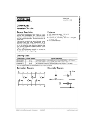
CD4069UBC
Absolute Maximum Ratings(Note 1)
(Note 2)
Recommended Operating
Conditions (Note 2)
Note 1: “Absolute Maximum Ratings” are those values beyond which the
safety of the device cannot be guaranteed. They are not meant to imply
that the devices should be operated at these limits. The table of “Recom-
mended Operating Conditions” and Electrical Characteristics table provide
conditions for actual device operation.
Note 2: VSS = 0V unless otherwise specified.
DC Electrical Characteristics (Note 3)
Note 3: VSS = 0V unless otherwise specified.
Note 4: IOH and IOL are tested one output at a time.
DC Supply Voltage (VDD) −0.5V to +18 VDC
Input Voltage (VIN) −0.5V to VDD +0.5 VDC
Storage Temperature Range (TS) −65°C to +150°C
Power Dissipation (PD)
Dual-In-Line 700 mW
Small Outline 500 mW
Lead Temperature (TL)
(Soldering, 10 seconds) 260°C
DC Supply Voltage (VDD) 3V to 15VDC
Input Voltage (VIN) 0V to VDD VDC
Operating Temperature Range (TA) −55°C to +125°C
Symbol Parameter Conditions
−55°C +25°C +125°C
Units
Min Max Min Typ Max Min Max
IDD Quiescent Device Current VDD = 5V, 0.25 0.25 7.5
µA
VIN = VDD or VSS
VDD = 10V, 0.5 0.5 15
VIN = VDD or VSS
VDD = 15V, 1.0 1.0 30
VIN = VDD or VSS
VOL LOW Level Output Voltage |IO| < 1 µA
VDD = 5V 0.05 0 0.05 0.05
VVDD = 10V 0.05 0 0.05 0.05
VDD = 15V 0.05 0 0.05 0.05
VOH HIGH Level Output Voltage |IO| < 1 µA
VDD = 5V 4.95 4.95 5 4.95
VVDD = 10V 9.95 9.95 10 9.95
VDD = 15V 14.95 14.95 15 14.95
VIL LOW Level Input Voltage |IO| < 1 µA
VDD = 5V, VO = 4.5V 1.0 1.0 1.0
VVDD = 10V, VO = 9V 2.0 2.0 2.0
VDD = 15V, VO = 13.5V 3.0 3.0 3.0
VIH HIGH Level Input Voltage |IO| < 1 µA
VDD = 5V, VO = 0.5V 4.0 4.0 4.0
VVDD = 10V, VO = 1V 8.0 8.0 8.0
VDD = 15V, VO = 1.5V 12.0 12.0 12.0
IOL LOW Level Output Current VDD = 5V, VO = 0.4V 0.64 0.51 0.88 0.36
mA(Note 4) VDD = 10V, VO = 0.5V 1.6 1.3 2.25 0.9
VDD = 15V, VO = 1.5V 4.2 3.4 8.8 2.4
IOH HIGH Level Output Current VDD = 5V, VO = 4.6V −0.64 −0.51 −0.88 −0.36
mA(Note 4) VDD = 10V, VO = 9.5V −1.6 −1.3 −2.25 −0.9
VDD = 15V, VO = 13.5V −4.2 −3.4 −8.8 −2.4
IIN Input Current VDD = 15V, VIN = 0V −0.1 −10−5
−0.1 −1.0
µA
VDD = 15V, VIN = 15V 0.1 10−5
0.1 1.0
3. 3 www.fairchildsemi.com
CD4069UBC
AC Electrical Characteristics (Note 5)
TA = 25°C, CL = 50 pF, RL = 200 kΩ, tr and tf ≤ 20 ns, unless otherwise specified
Note 5: AC Parameters are guaranteed by DC correlated testing.
Note 6: CPD determines the no load AC power consumption of any CMOS device. For complete explanation, see Family Characteristics application note—
AN-90.
AC Test Circuits and Switching Time Waveforms
Symbol Parameter Conditions Min Typ Max Units
tPHL or tPLH Propagation Delay Time from VDD = 5V 50 90
nsInput to Output VDD = 10V 30 60
VDD = 15V 25 50
tTHL or tTLH Transition Time VDD = 5V 80 150
nsVDD = 10V 50 100
VDD = 15V 40 80
CIN Average Input Capacitance Any Gate 6 15 pF
CPD Power Dissipation Capacitance Any Gate (Note 6) 12 pF
4. www.fairchildsemi.com 4
CD4069UBC
Typical Performance Characteristics
Gate Transfer Characteristics
Power Dissipation vs. Frequency
Propagation Delay vs. Ambient Temperature
Propagation Delay vs. Ambient Temperature
Propagation Delay Time vs. Load Capacitance
7. 7 www.fairchildsemi.com
CD4069UBCInverterCircuits
Physical Dimensions inches (millimeters) unless otherwise noted (Continued)
14-Lead Plastic Dual-In-Line Package (PDIP), JEDEC MS-001, 0.300" Wide
Package Number N14A
Fairchild does not assume any responsibility for use of any circuitry described, no circuit patent licenses are implied and
Fairchild reserves the right at any time without notice to change said circuitry and specifications.
LIFE SUPPORT POLICY
FAIRCHILD’S PRODUCTS ARE NOT AUTHORIZED FOR USE AS CRITICAL COMPONENTS IN LIFE SUPPORT
DEVICES OR SYSTEMS WITHOUT THE EXPRESS WRITTEN APPROVAL OF THE PRESIDENT OF FAIRCHILD
SEMICONDUCTOR CORPORATION. As used herein:
1. Life support devices or systems are devices or systems
which, (a) are intended for surgical implant into the
body, or (b) support or sustain life, and (c) whose failure
to perform when properly used in accordance with
instructions for use provided in the labeling, can be rea-
sonably expected to result in a significant injury to the
user.
2. A critical component in any component of a life support
device or system whose failure to perform can be rea-
sonably expected to cause the failure of the life support
device or system, or to affect its safety or effectiveness.
www.fairchildsemi.com