1. ■ Photomasks for Semiconductors
What is a photomask?
The photomask is an essential device to be
used in the manufacturing process of inte-
grated circuits such as LSI. It is a trans-
parent glass plate (composite quartz) on
which extremely fine microcircuit patterns
are etched on the light shielded film and
plays a role as the negative film (master)
when circuits are printed on silicon wafers.
Through application of photolithographic
technology, it becomes possible to plot
extremely fine patterns, which is not possi-
ble by any mechanical process. With this
process, a circuit pattern enlarged hun-
dreds of times is plotted first, and then the
pattern is reduced to its final size through
the photolithographic process. In the case
of the photomasks used for the manufac-
ture of super LSIs, because their concen-
tration level of circuits is much higher
than those on LSI, and because the pattern
is extremely fine, they are now manufac-
tured by utilizing the leading-edge electron
beam writing technology.
Toppan has been vigorously supporting
development of the semiconductor indus-
try through its manufacture of photomasks
since 1961. At the same time, in order to
satisfy the demand for much finer patterns
on evolving LSIs, we are continuously
developing phase-shifting masks and more
advanced photomask products using the
next generation of exposure technology.
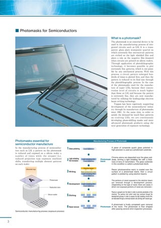
Photomasks essential for
semiconductor manufacture
In the manufacturing process of semiconduc-
tors such as LSI, a pattern on the photomask
is reduced and exposed on a silicon wafer a
number of times while the stepper (i.e.
reduced projection type exposure machine)
shifts, transferring multiple element patterns
on each wafer.
A
A
A
A
A
A
A
A
A
A
A
A
A
A
A
A
A
A
A
A
A
A
A
A
A
A
A
A
A
A
A
A
A
A
A
A
A
A
A
A
A
Ultraviolet rays
Photomask
Reduction lens
Silicon wafer
Semiconductor manufacturing process (exposure process)
1 Glass polishing
2
3 Writing
4 Development
5 Etching
6 Resist removal
A piece of composite quartz glass polished in
high precision is used as a photomask substrate.
Chrome atoms are deposited over the glass sub-
strate, forming a light shielding film with a thick-
ness of tens of nanometers. The glass substrate
in this condition is called a photomask blank.
Resist (photosensitive resin) is coated over the
surface of a photomask blank, then a circuit
pattern is plotted by using electron beams.
The portions of resist exposed to the electron beam
are removed through a development process.
(Depending on the type of resist, there are cases in
which non-exposed portions of resist are removed.)
Plasma is sprayed over the blank in order to promote penetration of the
chemical. The portions from which resist was removed through the
development process in order to expose the light shielding chrome film,
are fabricated through a chemical reaction (dry etching) with reactive gas.
A photomask is finally completed upon removal
of the resist. The photomask is then shipped
after passing several strict inspection processes.
Glass substrate
Light shielding film
Glass substrate
Light shielding film
Resist (photosensitive resin)
Glass substrate
Light shielding film
Glass substrate
Glass substrate
Electron beam
Glass substrate
▼ ▼
Photomask
blank
Photomask
Light shielding
film formation
Manufacturing Process of Photomask
3
2. Top in the world
Toppan's global strategy
In order to provide the globalizing
semiconductor market with prompt
and meticulous services, Toppan has a
manufacturing network of nine sites
throughout the world. It is the world's
sole supplier to have manufacturing
sites in all of North America, Europe
and the Asia/Pacific region.
Asaka Plant Plasma irradiation device
Operation of writing equipment Writing equipment
Design service for LSI
Toppan, as an LSI designing partner for leading semiconductor
manufacturers, has been providing designs and development of LSI
for over the past thirty years. A large number of such successful
development results encompasses various areas including analog
LSI, memories, LCDs, LED drivers and microcomputer logics.
Particularly, in the fields of RF
and analog mixed signal devel-
opment, we are broadly design-
ing power circuits, amplifier cir-
cuits, high frequency LSI and
digital consolidated macro for
system LSIs, and many others.
Toppan Technical Design Center is an expert in RF and analog mixed
signal LSI design.Toppan Technical Design Center Co., Ltd.
_Engineers supporting Toppan's LSI design business_
Toppan leads the world photomask market with
its superior technical capabilities
Along with the development of advanced technology node, multiple func-
tions and higher level performances of electronic devices, much finer fabri-
cation technologies are required in the manufacture of semiconductor prod-
ucts such as LSI. In this way, higher quality and more timely delivery is
also required of photomasks as the masters for semiconductor production.
Toppan regards the establishment of leading-edge technologies as one of
the most important issues in our management policy. We aim to differenti-
ate our technologies from others by positioning our Asaka Plant (Saitama
Prefecture in Japan) and Dresden Plant (Germany) as the base sites for
technology development and by concentrating resources such as engineers
and equipment to enhance the efficiency of such development.
In addition, we are actively tackling joint development of more extensive
technologies with semiconductor manufacturers such as IBM as well as var-
ious equipment, material and software manufacturers.
See the website. http://www.toptdc.com/en/
●Photomask production site
●Leading-edge technology development site
※Burlington is a joint development site with IBM.
■ Toppan's photomask production sites
●
●
●
Corbeil
Dresden ●●
●
●
●
Ichon
Shanghai
Shiga
Taoyuan
Asaka
●
●
●
Round Rock
Santa Clara
Burlington
●
North America
Europe Asia/Pacific
Electronics
4
Electronics
Toppan not only provides LSI
design services but also under-
takes the total solution services
for device manufacturing includ-
ing management of the entire
process and supply of LSI chips.
In addition to using its abundant
skill in designing, Toppan, by
incorporating various types of IPs
(design assets) as well as special-
ized analog technologies, enables
its customers to realize a timely
launch of new products that they
have planned. Furthermore, we
are able to realize unique LSIs
through alliances with competent
silicon foundries.
Device OEM FlowDevice OEM Flow
Customer
Quality Assurance
Interface A
System DesignSystem Design
RTL DesignRTL Design
Logic SynthesisLogic Synthesis
Layour DesignLayout Design
PhotomaskPhotomask
Wafer processWafer process
Wafer testWafer test
PackagingPackaging
Final testFinal test
Device OEM FlowDevice OEM Flow
Interface B
Interface C
Interface D
Interface E
Product(LSI)Product(LSI)
Outsourcing management systemOutsourcing management system
LSI sample production support
Volume production support
QualityAssurance
Device OEM