Probe cards are used in semiconductor testing to make contact with integrated circuits on wafers and chips. They allow electrical signals to be transmitted for thorough testing of functionality and performance. Probe cards consist of an array of microscopic needles attached to a printed circuit board. They play a crucial role in detecting early defects, ensuring consistent quality, and enabling mass production testing. As technology advances, probe cards must also evolve to accommodate smaller sizes, increased densities, and new technologies like 3D integrated circuits. Probe card manufacturers continue innovating to overcome challenges and meet the exacting demands of the semiconductor industry.
GraphRAG is All You need? LLM & Knowledge GraphGuy Korland
Guy Korland, CEO and Co-founder of FalkorDB, will review two articles on the integration of language models with knowledge graphs.
1. Unifying Large Language Models and Knowledge Graphs: A Roadmap.
https://arxiv.org/abs/2306.08302
2. Microsoft Research's GraphRAG paper and a review paper on various uses of knowledge graphs:
https://www.microsoft.com/en-us/research/blog/graphrag-unlocking-llm-discovery-on-narrative-private-data/
Essentials of Automations: Optimizing FME Workflows with ParametersSafe Software
Are you looking to streamline your workflows and boost your projects’ efficiency? Do you find yourself searching for ways to add flexibility and control over your FME workflows? If so, you’re in the right place.
Join us for an insightful dive into the world of FME parameters, a critical element in optimizing workflow efficiency. This webinar marks the beginning of our three-part “Essentials of Automation” series. This first webinar is designed to equip you with the knowledge and skills to utilize parameters effectively: enhancing the flexibility, maintainability, and user control of your FME projects.
Here’s what you’ll gain:
- Essentials of FME Parameters: Understand the pivotal role of parameters, including Reader/Writer, Transformer, User, and FME Flow categories. Discover how they are the key to unlocking automation and optimization within your workflows.
- Practical Applications in FME Form: Delve into key user parameter types including choice, connections, and file URLs. Allow users to control how a workflow runs, making your workflows more reusable. Learn to import values and deliver the best user experience for your workflows while enhancing accuracy.
- Optimization Strategies in FME Flow: Explore the creation and strategic deployment of parameters in FME Flow, including the use of deployment and geometry parameters, to maximize workflow efficiency.
- Pro Tips for Success: Gain insights on parameterizing connections and leveraging new features like Conditional Visibility for clarity and simplicity.
We’ll wrap up with a glimpse into future webinars, followed by a Q&A session to address your specific questions surrounding this topic.
Don’t miss this opportunity to elevate your FME expertise and drive your projects to new heights of efficiency.
Builder.ai Founder Sachin Dev Duggal's Strategic Approach to Create an Innova...Ramesh Iyer
In today's fast-changing business world, Companies that adapt and embrace new ideas often need help to keep up with the competition. However, fostering a culture of innovation takes much work. It takes vision, leadership and willingness to take risks in the right proportion. Sachin Dev Duggal, co-founder of Builder.ai, has perfected the art of this balance, creating a company culture where creativity and growth are nurtured at each stage.
Securing your Kubernetes cluster_ a step-by-step guide to success !KatiaHIMEUR1
Today, after several years of existence, an extremely active community and an ultra-dynamic ecosystem, Kubernetes has established itself as the de facto standard in container orchestration. Thanks to a wide range of managed services, it has never been so easy to set up a ready-to-use Kubernetes cluster.
However, this ease of use means that the subject of security in Kubernetes is often left for later, or even neglected. This exposes companies to significant risks.
In this talk, I'll show you step-by-step how to secure your Kubernetes cluster for greater peace of mind and reliability.
Generating a custom Ruby SDK for your web service or Rails API using Smithyg2nightmarescribd
Have you ever wanted a Ruby client API to communicate with your web service? Smithy is a protocol-agnostic language for defining services and SDKs. Smithy Ruby is an implementation of Smithy that generates a Ruby SDK using a Smithy model. In this talk, we will explore Smithy and Smithy Ruby to learn how to generate custom feature-rich SDKs that can communicate with any web service, such as a Rails JSON API.
UiPath Test Automation using UiPath Test Suite series, part 4DianaGray10
Welcome to UiPath Test Automation using UiPath Test Suite series part 4. In this session, we will cover Test Manager overview along with SAP heatmap.
The UiPath Test Manager overview with SAP heatmap webinar offers a concise yet comprehensive exploration of the role of a Test Manager within SAP environments, coupled with the utilization of heatmaps for effective testing strategies.
Participants will gain insights into the responsibilities, challenges, and best practices associated with test management in SAP projects. Additionally, the webinar delves into the significance of heatmaps as a visual aid for identifying testing priorities, areas of risk, and resource allocation within SAP landscapes. Through this session, attendees can expect to enhance their understanding of test management principles while learning practical approaches to optimize testing processes in SAP environments using heatmap visualization techniques
What will you get from this session?
1. Insights into SAP testing best practices
2. Heatmap utilization for testing
3. Optimization of testing processes
4. Demo
Topics covered:
Execution from the test manager
Orchestrator execution result
Defect reporting
SAP heatmap example with demo
Speaker:
Deepak Rai, Automation Practice Lead, Boundaryless Group and UiPath MVP
Connector Corner: Automate dynamic content and events by pushing a buttonDianaGray10
Here is something new! In our next Connector Corner webinar, we will demonstrate how you can use a single workflow to:
Create a campaign using Mailchimp with merge tags/fields
Send an interactive Slack channel message (using buttons)
Have the message received by managers and peers along with a test email for review
But there’s more:
In a second workflow supporting the same use case, you’ll see:
Your campaign sent to target colleagues for approval
If the “Approve” button is clicked, a Jira/Zendesk ticket is created for the marketing design team
But—if the “Reject” button is pushed, colleagues will be alerted via Slack message
Join us to learn more about this new, human-in-the-loop capability, brought to you by Integration Service connectors.
And...
Speakers:
Akshay Agnihotri, Product Manager
Charlie Greenberg, Host
LF Energy Webinar: Electrical Grid Modelling and Simulation Through PowSyBl -...DanBrown980551
Do you want to learn how to model and simulate an electrical network from scratch in under an hour?
Then welcome to this PowSyBl workshop, hosted by Rte, the French Transmission System Operator (TSO)!
During the webinar, you will discover the PowSyBl ecosystem as well as handle and study an electrical network through an interactive Python notebook.
PowSyBl is an open source project hosted by LF Energy, which offers a comprehensive set of features for electrical grid modelling and simulation. Among other advanced features, PowSyBl provides:
- A fully editable and extendable library for grid component modelling;
- Visualization tools to display your network;
- Grid simulation tools, such as power flows, security analyses (with or without remedial actions) and sensitivity analyses;
The framework is mostly written in Java, with a Python binding so that Python developers can access PowSyBl functionalities as well.
What you will learn during the webinar:
- For beginners: discover PowSyBl's functionalities through a quick general presentation and the notebook, without needing any expert coding skills;
- For advanced developers: master the skills to efficiently apply PowSyBl functionalities to your real-world scenarios.
The Art of the Pitch: WordPress Relationships and SalesLaura Byrne
Clients don’t know what they don’t know. What web solutions are right for them? How does WordPress come into the picture? How do you make sure you understand scope and timeline? What do you do if sometime changes?
All these questions and more will be explored as we talk about matching clients’ needs with what your agency offers without pulling teeth or pulling your hair out. Practical tips, and strategies for successful relationship building that leads to closing the deal.
Kubernetes & AI - Beauty and the Beast !?! @KCD Istanbul 2024Tobias Schneck
As AI technology is pushing into IT I was wondering myself, as an “infrastructure container kubernetes guy”, how get this fancy AI technology get managed from an infrastructure operational view? Is it possible to apply our lovely cloud native principals as well? What benefit’s both technologies could bring to each other?
Let me take this questions and provide you a short journey through existing deployment models and use cases for AI software. On practical examples, we discuss what cloud/on-premise strategy we may need for applying it to our own infrastructure to get it to work from an enterprise perspective. I want to give an overview about infrastructure requirements and technologies, what could be beneficial or limiting your AI use cases in an enterprise environment. An interactive Demo will give you some insides, what approaches I got already working for real.
State of ICS and IoT Cyber Threat Landscape Report 2024 previewPrayukth K V
The IoT and OT threat landscape report has been prepared by the Threat Research Team at Sectrio using data from Sectrio, cyber threat intelligence farming facilities spread across over 85 cities around the world. In addition, Sectrio also runs AI-based advanced threat and payload engagement facilities that serve as sinks to attract and engage sophisticated threat actors, and newer malware including new variants and latent threats that are at an earlier stage of development.
The latest edition of the OT/ICS and IoT security Threat Landscape Report 2024 also covers:
State of global ICS asset and network exposure
Sectoral targets and attacks as well as the cost of ransom
Global APT activity, AI usage, actor and tactic profiles, and implications
Rise in volumes of AI-powered cyberattacks
Major cyber events in 2024
Malware and malicious payload trends
Cyberattack types and targets
Vulnerability exploit attempts on CVEs
Attacks on counties – USA
Expansion of bot farms – how, where, and why
In-depth analysis of the cyber threat landscape across North America, South America, Europe, APAC, and the Middle East
Why are attacks on smart factories rising?
Cyber risk predictions
Axis of attacks – Europe
Systemic attacks in the Middle East
Download the full report from here:
https://sectrio.com/resources/ot-threat-landscape-reports/sectrio-releases-ot-ics-and-iot-security-threat-landscape-report-2024/
State of ICS and IoT Cyber Threat Landscape Report 2024 preview
What is a Probe Card, and what Role Does it Play in Semiconductor Testing
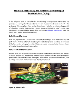
1. What is a Probe Card, and what Role Does it Play in
Semiconductor Testing?
In the fast-paced realm of semiconductor manufacturing, where precision and reliability are
paramount, a seemingly humble yet critical component plays a silent yet indispensable role – the
probe card. This unsung hero of the semiconductor industry is the key to unlocking the potential
of microchips, ensuring they meet the rigorous standards required for today's cutting-edge
technologies. In this exploration, we will delve into what a Probe Card Manufacturer is and the
pivotal role it plays in semiconductor testing.
Definition and Purpose:
At its core, a probe card is a device used in semiconductor testing to assess the functionality and
performance of integrated circuits (ICs) during the production process. Essentially, it serves as a
bridge between the testing equipment and the semiconductor wafer, facilitating the transmission
of electrical signals for thorough examination.
Components and Construction:
A typical probe card consists of a printed circuit board (PCB) with an array of microscopic needles,
or probes, attached to it. These probes are meticulously designed to make contact with specific
points on the semiconductor wafer, enabling the measurement of electrical characteristics, such
as voltage and current, at different nodes of the integrated circuit.
Types of Probe Cards:
2. There are various types of probe cards, each tailored for specific testing applications. The two
primary categories are known as wafer probe cards and final test probe cards. Wafer probe cards
are used in the early stages of semiconductor manufacturing to assess the performance of
individual dies on a wafer. On the other hand, final test probe cards are employed in the later
stages to evaluate the fully assembled semiconductor devices.
The Crucial Role of Probe Cards in Semiconductor Testing:
• Early Detection of Defects
One of the primary functions of Probe Card Manufacturers is to identify defects in the
semiconductor devices before they progress further in the manufacturing process. By making
contact with each die on a wafer, the probe card can assess whether the integrated circuits meet
the specified electrical parameters. This early detection is crucial for minimizing waste and
optimizing the overall production yield.
1. Ensuring Consistent Quality
As technology advances, semiconductor devices become more complex and densely packed with
components. The precision of probe cards becomes increasingly vital in ensuring that each chip
meets the stringent quality standards required for applications ranging from consumer
electronics to critical industrial systems. Probe cards play a pivotal role in guaranteeing the
uniformity and reliability of the final products.
2. Facilitating Parametric Testing
Parametric testing involves evaluating the performance of individual components within a
semiconductor device. Probe cards enable this by allowing precise measurements of various
electrical parameters, such as voltage, current, and resistance, across different points on the
integrated circuit. This level of detailed testing ensures that each chip meets the specified
performance criteria.
3. Enabling Mass Production
In semiconductor manufacturing, efficiency is key. Probe cards contribute to the acceleration of
production processes by swiftly and accurately testing multiple dies simultaneously. This high-
throughput capability is essential for meeting the demands of the ever-expanding electronics
market and delivering cost-effective solutions.
Evolution of Probe Card Technology:
• Miniaturization and Increased Density
3. As semiconductor technology continues to advance, the demand for smaller and more powerful
devices grows. Probe cards have evolved to keep pace with this trend, featuring miniaturized
probes and increased probe density. This allows for testing the latest generation of integrated
circuits, which often have smaller dimensions and more intricate designs.
• Enhanced Precision and Reliability
The relentless pursuit of higher performance has driven innovations in Probe Card Manufacturers'
technology, leading to enhanced precision and reliability. The materials used in probe
construction, as well as the manufacturing processes, have been refined to meet the exacting
requirements of modern semiconductor testing. This evolution ensures that probe cards can
effectively interface with the increasingly sophisticated semiconductor devices being produced.
• Integration of Advanced Technologies
Incorporating advanced technologies such as artificial intelligence (AI) and machine learning has
become a hallmark of the latest probe card designs. These technologies enhance the efficiency
of testing processes, allowing for adaptive testing strategies and real-time adjustments based on
the evolving characteristics of semiconductor devices.
Overcoming Challenges in Probe Card Technology:
• Contact Wear and Tear
One of the primary challenges in probe card technology is the wear and tear of the microscopic
probes. Repeated contact with semiconductor wafers can lead to degradation over time, affecting
the accuracy and reliability of the testing process. Manufacturers address this challenge through
the use of durable materials and innovative probe designs to extend the lifespan of probe cards.
• Compatibility with Diverse Semiconductor Designs
With the increasing diversity in semiconductor designs, probe cards must be versatile enough to
accommodate various layouts and configurations. Adaptable probe card designs, often featuring
customizable probe arrangements, ensure compatibility with the wide array of integrated circuits
produced by different manufacturers.
• Balancing Cost and Performance
Manufacturers face the perpetual challenge of striking a balance between the cost of probe card
production and the performance they deliver. As the semiconductor industry demands higher
testing accuracy and throughput, optimizing the cost-effectiveness of probe cards becomes a
critical consideration for both manufacturers and end-users.
4. The Future of Probe Cards Innovations and Trends:
• Integration of 3D IC Technology
The rise of three-dimensional integrated circuit (3D IC) technology presents new challenges and
opportunities for probe cards. As semiconductor devices become stacked vertically to achieve
higher performance and efficiency, probe cards must evolve to accommodate this three-
dimensional landscape. Innovations in probe card design are underway to ensure seamless
testing of 3D ICs.
• Smart Probe Cards with Autonomous Testing
The integration of smart technologies, including autonomous testing capabilities, is on the
horizon for probe cards. Smart probe cards equipped with sensors and intelligent algorithms can
adapt to changing testing conditions, identify potential issues, and make real-time adjustments.
This promises to further enhance testing efficiency and reduce the need for manual intervention.
• Sustainability and Environmental Considerations
In an era where environmental sustainability is a growing concern, the semiconductor industry,
including probe card manufacturers, is exploring ways to minimize its ecological footprint.
Sustainable materials and manufacturing processes are being explored to create probe cards that
align with the principles of environmental responsibility.
Conclusion:
Probe cards play a pivotal role in semiconductor testing, ensuring the reliability, quality, and
performance of the integrated circuits that power our modern world. As technology continues to
advance, Probe Card technology evolves in tandem, overcoming challenges and embracing
innovations to meet the demands of an ever-changing semiconductor landscape. The unseen
heroes of semiconductor testing, probe cards stand as a testament to the intricate and
interconnected nature of the processes that drive the heart of our digital age.