Downloaded 27 times


![RM0008 List of tables
Table 201. Minimum duration for soft disconnect . . . . . . . . . . . . . . . . . . . . . . . . . . . . . . . . . . . . . . . . 840
Table 202. OTG_FS register map and reset values . . . . . . . . . . . . . . . . . . . . . . . . . . . . . . . . . . . . . . 861
Table 203. Ethernet pin configuration . . . . . . . . . . . . . . . . . . . . . . . . . . . . . . . . . . . . . . . . . . . . . . . . . 915
Table 204. Management frame format . . . . . . . . . . . . . . . . . . . . . . . . . . . . . . . . . . . . . . . . . . . . . . . . 917
Table 205. Clock range. . . . . . . . . . . . . . . . . . . . . . . . . . . . . . . . . . . . . . . . . . . . . . . . . . . . . . . . . . . . 919
Table 206. TX interface signal encoding . . . . . . . . . . . . . . . . . . . . . . . . . . . . . . . . . . . . . . . . . . . . . . 921
Table 207. RX interface signal encoding . . . . . . . . . . . . . . . . . . . . . . . . . . . . . . . . . . . . . . . . . . . . . . 921
Table 208. Frame statuses . . . . . . . . . . . . . . . . . . . . . . . . . . . . . . . . . . . . . . . . . . . . . . . . . . . . . . . . . 937
Table 209. Destination address filtering table. . . . . . . . . . . . . . . . . . . . . . . . . . . . . . . . . . . . . . . . . . . 942
Table 210. Source address filtering table . . . . . . . . . . . . . . . . . . . . . . . . . . . . . . . . . . . . . . . . . . . . . . 943
Table 211. Receive descriptor 0 . . . . . . . . . . . . . . . . . . . . . . . . . . . . . . . . . . . . . . . . . . . . . . . . . . . . . 975
Table 212. Ethernet register map and reset values . . . . . . . . . . . . . . . . . . . . . . . . . . . . . . . . . . . . . 1021
Table 213. SWJ debug port pins . . . . . . . . . . . . . . . . . . . . . . . . . . . . . . . . . . . . . . . . . . . . . . . . . . . 1030
Table 214. Flexible SWJ-DP pin assignment . . . . . . . . . . . . . . . . . . . . . . . . . . . . . . . . . . . . . . . . . . 1031
Table 215. JTAG debug port data registers . . . . . . . . . . . . . . . . . . . . . . . . . . . . . . . . . . . . . . . . . . . 1035
Table 216. 32-bit debug port registers addressed through the shifted value A[3:2] . . . . . . . . . . . . . 1037
Table 217. Packet request (8-bits) . . . . . . . . . . . . . . . . . . . . . . . . . . . . . . . . . . . . . . . . . . . . . . . . . . 1038
Table 218. ACK response (3 bits). . . . . . . . . . . . . . . . . . . . . . . . . . . . . . . . . . . . . . . . . . . . . . . . . . . 1038
Table 219. DATA transfer (33 bits) . . . . . . . . . . . . . . . . . . . . . . . . . . . . . . . . . . . . . . . . . . . . . . . . . . 1038
Table 220. SW-DP registers . . . . . . . . . . . . . . . . . . . . . . . . . . . . . . . . . . . . . . . . . . . . . . . . . . . . . . . 1039
Table 221. Cortex-M3 AHB-AP registers . . . . . . . . . . . . . . . . . . . . . . . . . . . . . . . . . . . . . . . . . . . . . 1041
Table 222. Core debug registers . . . . . . . . . . . . . . . . . . . . . . . . . . . . . . . . . . . . . . . . . . . . . . . . . . . 1041
Table 223. Main ITM registers . . . . . . . . . . . . . . . . . . . . . . . . . . . . . . . . . . . . . . . . . . . . . . . . . . . . . 1044
Table 224. Main ETM registers. . . . . . . . . . . . . . . . . . . . . . . . . . . . . . . . . . . . . . . . . . . . . . . . . . . . . 1046
Table 225. Asynchronous TRACE pin assignment. . . . . . . . . . . . . . . . . . . . . . . . . . . . . . . . . . . . . . 1050
Table 226. Synchronous TRACE pin assignment . . . . . . . . . . . . . . . . . . . . . . . . . . . . . . . . . . . . . . 1050
Table 227. Flexible TRACE pin assignment . . . . . . . . . . . . . . . . . . . . . . . . . . . . . . . . . . . . . . . . . . . 1051
Table 228. Important TPIU registers. . . . . . . . . . . . . . . . . . . . . . . . . . . . . . . . . . . . . . . . . . . . . . . . . 1054
Table 229. DBG register map and reset values . . . . . . . . . . . . . . . . . . . . . . . . . . . . . . . . . . . . . . . . 1055
Table 230. Document revision history . . . . . . . . . . . . . . . . . . . . . . . . . . . . . . . . . . . . . . . . . . . . . . . 1056
Doc ID 13902 Rev 11 31/1072](https://image.slidesharecdn.com/stm32referencemanual-110220082754-phpapp01/85/Stm32-reference-manual-31-320.jpg)


![Memory and bus architecture RM0008
Flash access control register (FLASH_ACR)
Address offset: 0x00
Reset value: 0x0000 0030
31 30 29 28 27 26 25 24 23 22 21 20 19 18 17 16
Reserved
15 14 13 12 11 10 9 8 7 6 5 4 3 2 1 0
PRFTBS PRFTBE HLFCYA LATENCY
Reserved
r rw rw rw rw rw
Bits 31:6 Reserved, must be kept cleared.
Bit 5 PRFTBS: Prefetch buffer status
This bit provides the status of the prefetch buffer.
0: Prefetch buffer is disabled
1: Prefetch buffer is enabled
Bit 4 PRFTBE: Prefetch buffer enable
0: Prefetch is disabled
1: Prefetch is enabled
Bit 3 HLFCYA: Flash half cycle access enable
0: Half cycle is disabled
1: Half cycle is enabled
Bits 2:0 LATENCY: Latency
These bits represent the ratio of the SYSCLK (system clock) period to the Flash access
time.
000 Zero wait state, if 0 < SYSCLK 24 MHz
001 One wait state, if 24 MHz < SYSCLK 48 MHz
010 Two wait states, if 48 MHz < SYSCLK 72 MHz
2.4 Boot configuration
In the STM32F10xxx, 3 different boot modes can be selected through BOOT[1:0] pins as
shown in Table 7.
Table 7. Boot modes
Boot mode selection pins
Boot mode Aliasing
BOOT1 BOOT0
x 0 Main Flash memory Main Flash memory is selected as boot space
0 1 System memory System memory is selected as boot space
1 1 Embedded SRAM Embedded SRAM is selected as boot space
The values on the BOOT pins are latched on the 4th rising edge of SYSCLK after a reset. It
is up to the user to set the BOOT1 and BOOT0 pins after Reset to select the required boot
mode.
The BOOT pins are also re-sampled when exiting from Standby mode. Consequently they
must be kept in the required Boot mode configuration in Standby mode. After this startup
54/1072 Doc ID 13902 Rev 11](https://image.slidesharecdn.com/stm32referencemanual-110220082754-phpapp01/85/Stm32-reference-manual-54-320.jpg)


![RM0008 CRC calculation unit
3.3 CRC functional description
The CRC calculation unit mainly consists of a single 32-bit data register, which:
● is used as an input register to enter new data in the CRC calculator (when writing into
the register)
● holds the result of the previous CRC calculation (when reading the register)
Each write operation into the data register creates a combination of the previous CRC value
and the new one (CRC computation is done on the whole 32-bit data word, and not byte per
byte).
The write operation is stalled until the end of the CRC computation, thus allowing back-to-
back write accesses or consecutive write and read accesses.
The CRC calculator can be reset to FFFF FFFFh with the RESET control bit in the CRC_CR
register. This operation does not affect the contents of the CRC_IDR register.
3.4 CRC registers
The CRC calculation unit contains two data registers and a control register.
3.4.1 Data register (CRC_DR)
Address offset: 0x00
Reset value: 0xFFFF FFFF
31 30 29 28 27 26 25 24 23 22 21 20 19 18 17 16
DR [31:16]
rw rw rw rw rw rw rw rw rw rw rw rw rw rw rw rw
15 14 13 12 11 10 9 8 7 6 5 4 3 2 1 0
DR [15:0]
rw rw rw rw rw rw rw rw rw rw rw rw rw rw rw rw
Bits 31:0 Data register bits
Used as an input register when writing new data into the CRC calculator.
Holds the previous CRC calculation result when it is read.
3.4.2 Independent data register (CRC_IDR)
Address offset: 0x04
Reset value: 0x0000 0000
15 14 13 12 11 10 9 8 7 6 5 4 3 2 1 0
IDR[7:0]
Reserved
rw rw rw rw rw rw rw rw
Bits 31:8 Reserved
Doc ID 13902 Rev 11 57/1072](https://image.slidesharecdn.com/stm32referencemanual-110220082754-phpapp01/85/Stm32-reference-manual-57-320.jpg)


![Power control (PWR) RM0008
4.1.3 Voltage regulator
The voltage regulator is always enabled after Reset. It works in three different modes
depending on the application modes.
● In Run mode, the regulator supplies full power to the 1.8 V domain (core, memories
and digital peripherals).
● In Stop mode the regulator supplies low-power to the 1.8 V domain, preserving
contents of registers and SRAM
● In Standby Mode, the regulator is powered off. The contents of the registers and SRAM
are lost except for the Standby circuitry and the Backup Domain.
4.2 Power supply supervisor
4.2.1 Power on reset (POR)/power down reset (PDR)
The device has an integrated POR/PDR circuitry that allows proper operation starting
from/down to 2 V.
The device remains in Reset mode when VDD/VDDA is below a specified threshold,
VPOR/PDR, without the need for an external reset circuit. For more details concerning the
power on/power down reset threshold, refer to the electrical characteristics of the datasheet.
Figure 5. Power on reset/power down reset waveform
VDD/VDDA
POR
40 mV
hysteresis
PDR
Temporization
tRSTTEMPO
Reset
4.2.2 Programmable voltage detector (PVD)
You can use the PVD to monitor the VDD/VDDA power supply by comparing it to a threshold
selected by the PLS[2:0] bits in the Power control register (PWR_CR).
The PVD is enabled by setting the PVDE bit.
A PVDO flag is available, in the Power control/status register (PWR_CSR), to indicate if
VDD/VDDA is higher or lower than the PVD threshold. This event is internally connected to
the EXTI line16 and can generate an interrupt if enabled through the EXTI registers. The
62/1072 Doc ID 13902 Rev 11](https://image.slidesharecdn.com/stm32referencemanual-110220082754-phpapp01/85/Stm32-reference-manual-62-320.jpg)


![RM0008 Power control (PWR)
Debug mode
By default, the debug connection is lost if the application puts the MCU in Stop or Standby
mode while the debug features are used. This is due to the fact that the Cortex™-M3 core is
no longer clocked.
However, by setting some configuration bits in the DBGMCU_CR register, the software can
be debugged even when using the low-power modes extensively. For more details, refer to
Section 30.16.1: Debug support for low-power modes.
4.3.6 Auto-wakeup (AWU) from low-power mode
The RTC can be used to wakeup the MCU from low-power mode without depending on an
external interrupt (Auto-wakeup mode). The RTC provides a programmable time base for
waking up from Stop or Standby mode at regular intervals. For this purpose, two of the three
alternative RTC clock sources can be selected by programming the RTCSEL[1:0] bits in the
Backup domain control register (RCC_BDCR):
● Low-power 32.768 kHz external crystal oscillator (LSE OSC).
This clock source provides a precise time base with very low-power consumption (less
than 1µA added consumption in typical conditions)
● Low-power internal RC Oscillator (LSI RC)
This clock source has the advantage of saving the cost of the 32.768 kHz crystal. This
internal RC Oscillator is designed to add minimum power consumption.
To wakeup from Stop mode with an RTC alarm event, it is necessary to:
● Configure the EXTI Line 17 to be sensitive to rising edge
● Configure the RTC to generate the RTC alarm
To wakeup from Standby mode, there is no need to configure the EXTI Line 17.
4.4 Power control registers
The peripheral registers can be accessed by half-words (16-bit) or words (32-bit).
4.4.1 Power control register (PWR_CR)
Address offset: 0x00
Reset value: 0x0000 0000 (reset by wakeup from Standby mode)
31 30 29 28 27 26 25 24 23 22 21 20 19 18 17 16
Reserved
15 14 13 12 11 10 9 8 7 6 5 4 3 2 1 0
DBP PLS[2:0] PVDE CSBF CWUF PDDS LPDS
Reserved
rw rw rw rw rw rc_w1 rc_w1 rw rw
Bits 31:9 Reserved, always read as 0.
Doc ID 13902 Rev 11 69/1072](https://image.slidesharecdn.com/stm32referencemanual-110220082754-phpapp01/85/Stm32-reference-manual-69-320.jpg)
![Power control (PWR) RM0008
Bit 8 DBP: Disable backup domain write protection.
In reset state, the RTC and backup registers are protected against parasitic write access.
This bit must be set to enable write access to these registers.
0: Access to RTC and Backup registers disabled
1: Access to RTC and Backup registers enabled
Note: If the HSE divided by 128 is used as the RTC clock, this bit must remain set to 1.
Bits 7:5 PLS[2:0]: PVD level selection.
These bits are written by software to select the voltage threshold detected by the Power
Voltage Detector
000: 2.2V
001: 2.3V
010: 2.4V
011: 2.5V
100: 2.6V
101: 2.7V
110: 2.8V
111: 2.9V
Note: Refer to the electrical characteristics of the datasheet for more details.
Bit 4 PVDE: Power voltage detector enable.
This bit is set and cleared by software.
0: PVD disabled
1: PVD enabled
Bit 3 CSBF: Clear standby flag.
This bit is always read as 0.
0: No effect
1: Clear the SBF Standby Flag (write).
Bit 2 CWUF: Clear wakeup flag.
This bit is always read as 0.
0: No effect
1: Clear the WUF Wakeup Flag after 2 System clock cycles. (write)
Bit 1 PDDS: Power down deepsleep.
This bit is set and cleared by software. It works together with the LPDS bit.
0: Enter Stop mode when the CPU enters Deepsleep. The regulator status depends on the
LPDS bit.
1: Enter Standby mode when the CPU enters Deepsleep.
Bit 0 LPDS: Low-power deepsleep.
This bit is set and cleared by software. It works together with the PDDS bit.
0: Voltage regulator on during Stop mode
1: Voltage regulator in low-power mode during Stop mode
70/1072 Doc ID 13902 Rev 11](https://image.slidesharecdn.com/stm32referencemanual-110220082754-phpapp01/85/Stm32-reference-manual-70-320.jpg)
![RM0008 Power control (PWR)
4.4.2 Power control/status register (PWR_CSR)
Address offset: 0x04
Reset value: 0x0000 0000 (not reset by wakeup from Standby mode)
Additional APB cycles are needed to read this register versus a standard APB read.
31 30 29 28 27 26 25 24 23 22 21 20 19 18 17 16
Reserved
15 14 13 12 11 10 9 8 7 6 5 4 3 2 1 0
EWUP PVDO SBF WUF
Reserved Reserved
rw r r r
Bits 31:9 Reserved, always read as 0.
Bit 8 EWUP: Enable WKUP pin
This bit is set and cleared by software.
0: WKUP pin is used for general purpose I/O. An event on the WKUP pin does not wakeup
the device from Standby mode.
1: WKUP pin is used for wakeup from Standby mode and forced in input pull down
configuration (rising edge on WKUP pin wakes-up the system from Standby mode).
Note: This bit is reset by a system Reset.
Bits 7:3 Reserved, always read as 0.
Bit 2 PVDO: PVD output
This bit is set and cleared by hardware. It is valid only if PVD is enabled by the PVDE bit.
0: VDD/VDDA is higher than the PVD threshold selected with the PLS[2:0] bits.
1: VDD/VDDA is lower than the PVD threshold selected with the PLS[2:0] bits.
Note: The PVD is stopped by Standby mode. For this reason, this bit is equal to 0 after
Standby or reset until the PVDE bit is set.
Bit 1 SBF: Standby flag
This bit is set by hardware and cleared only by a POR/PDR (power on reset/power down reset)
or by setting the CSBF bit in the Power control register (PWR_CR)
0: Device has not been in Standby mode
1: Device has been in Standby mode
Bit 0 WUF: Wakeup flag
This bit is set by hardware and cleared only by a POR/PDR (power on reset/power down
reset) or by setting the CWUF bit in the Power control register (PWR_CR)
0: No wakeup event occurred
1: A wakeup event was received from the WKUP pin or from the RTC alarm
Note: An additional wakeup event is detected if the WKUP pin is enabled (by setting the
EWUP bit) when the WKUP pin level is already high.
Doc ID 13902 Rev 11 71/1072](https://image.slidesharecdn.com/stm32referencemanual-110220082754-phpapp01/85/Stm32-reference-manual-71-320.jpg)
![Power control (PWR) RM0008
4.4.3 PWR register map
The following table summarizes the PWR registers.
Table 14. PWR register map and reset values
31
30
29
28
27
26
25
24
23
22
21
20
19
18
17
16
15
14
13
12
11
10
Offset Register
9
8
7
6
5
4
3
2
1
0
CWUF
PDDS
PVDE
CSBF
LPDS
DBP
PWR_CR PLS[2:0]
0x000 Reserved
Reset value 0 0 0 0 0 0 0 0 0
EWUP
PVDO
WUF
SBF
PWR_CSR
0x004 Reserved Reserved
Reset value 0 0 0 0
Refer to Table 1 on page 44 for the register boundary addresses.
72/1072 Doc ID 13902 Rev 11](https://image.slidesharecdn.com/stm32referencemanual-110220082754-phpapp01/85/Stm32-reference-manual-72-320.jpg)

![Backup registers (BKP) RM0008
5.3 BKP functional description
5.3.1 Tamper detection
The TAMPER pin generates a Tamper detection event when the pin changes from 0 to 1 or
from 1 to 0 depending on the TPAL bit in the Backup control register (BKP_CR). A tamper
detection event resets all data backup registers.
However to avoid losing Tamper events, the signal used for edge detection is logically
ANDed with the Tamper enable in order to detect a Tamper event in case it occurs before
the TAMPER pin is enabled.
● When TPAL=0: If the TAMPER pin is already high before it is enabled (by setting TPE
bit), an extra Tamper event is detected as soon as the TAMPER pin is enabled (while
there was no rising edge on the TAMPER pin after TPE was set)
● When TPAL=1: If the TAMPER pin is already low before it is enabled (by setting the
TPE bit), an extra Tamper event is detected as soon as the TAMPER pin is enabled
(while there was no falling edge on the TAMPER pin after TPE was set)
By setting the TPIE bit in the BKP_CSR register, an interrupt is generated when a Tamper
detection event occurs.
After a Tamper event has been detected and cleared, the TAMPER pin should be disabled
and then re-enabled with TPE before writing to the backup data registers (BKP_DRx) again.
This prevents software from writing to the backup data registers (BKP_DRx), while the
TAMPER pin value still indicates a Tamper detection. This is equivalent to a level detection
on the TAMPER pin.
Note: Tamper detection is still active when VDD power is switched off. To avoid unwanted resetting
of the data backup registers, the TAMPER pin should be externally tied to the correct level.
5.3.2 RTC calibration
For measurement purposes, the RTC clock with a frequency divided by 64 can be output on
the TAMPER pin. This is enabled by setting the CCO bit in the RTC clock calibration register
(BKP_RTCCR).
The clock can be slowed down by up to 121 ppm by configuring CAL[6:0] bits.
For more details about RTC calibration and how to use it to improve timekeeping accuracy,
please refer to AN2604 "STM32F101xx and STM32F103xx RTC calibration”.
74/1072 Doc ID 13902 Rev 11](https://image.slidesharecdn.com/stm32referencemanual-110220082754-phpapp01/85/Stm32-reference-manual-74-320.jpg)
![RM0008 Backup registers (BKP)
5.4 BKP registers
Refer to Section 1.1 on page 40 for a list of abbreviations used in register descriptions.
The peripheral registers can be accessed by half-words (16-bit) or words (32-bit).
5.4.1 Backup data register x (BKP_DRx) (x = 1 ..42)
Address offset: 0x04 to 0x28, 0x40 to 0xBC
Reset value: 0x0000 0000
15 14 13 12 11 10 9 8 7 6 5 4 3 2 1 0
D[15:0]
rw rw rw rw rw rw rw rw rw rw rw rw rw rw rw rw
Bits 15:0 D[15:0] Backup data
These bits can be written with user data.
Note: The BKP_DRx registers are not reset by a System reset or Power reset or when the
device wakes up from Standby mode.
They are reset by a Backup Domain reset or by a TAMPER pin event (if the TAMPER
pin function is activated).
5.4.2 RTC clock calibration register (BKP_RTCCR)
Address offset: 0x2C
Reset value: 0x0000 0000
15 14 13 12 11 10 9 8 7 6 5 4 3 2 1 0
ASOS ASOE CCO CAL[6:0]
Reserved
rw rw rw rw rw rw rw rw rw rw
Bits 15:10 Reserved, always read as 0.
Bit 9 ASOS: Alarm or second output selection
When the ASOE bit is set, the ASOS bit can be used to select whether the signal output on
the TAMPER pin is the RTC Second pulse signal or the Alarm pulse signal:
0: RTC Alarm pulse output selected
1: RTC Second pulse output selected
Note: This bit is reset only by a Backup domain reset.
Bit 8 ASOE: Alarm or second output enable
Setting this bit outputs either the RTC Alarm pulse signal or the Second pulse signal on the
TAMPER pin depending on the ASOS bit.
The output pulse duration is one RTC clock period. The TAMPER pin must not be enabled
while the ASOE bit is set.
Note: This bit is reset only by a Backup domain reset.
Bit 7 CCO: Calibration clock output
0: No effect
1: Setting this bit outputs the RTC clock with a frequency divided by 64 on the TAMPER pin.
The TAMPER pin must not be enabled while the CCO bit is set in order to avoid unwanted
Tamper detection.
Note: This bit is reset when the VDD supply is powered off.
Doc ID 13902 Rev 11 75/1072](https://image.slidesharecdn.com/stm32referencemanual-110220082754-phpapp01/85/Stm32-reference-manual-75-320.jpg)
![Backup registers (BKP) RM0008
Bit 6:0 CAL[6:0]: Calibration value
This value indicates the number of clock pulses that will be ignored every 2^20 clock pulses.
This allows the calibration of the RTC, slowing down the clock by steps of 1000000/2^20
PPM.
The clock of the RTC can be slowed down from 0 to 121PPM.
5.4.3 Backup control register (BKP_CR)
Address offset: 0x30
Reset value: 0x0000 0000
15 14 13 12 11 10 9 8 7 6 5 4 3 2 1 0
TPAL TPE
Reserved
rw rw
Bits 15:2 Reserved, always read as 0.
Bit 1 TPAL: TAMPER pin active level
0: A high level on the TAMPER pin resets all data backup registers (if TPE bit is set).
1: A low level on the TAMPER pin resets all data backup registers (if TPE bit is set).
Bit 0 TPE: TAMPER pin enable
0: The TAMPER pin is free for general purpose I/O
1: Tamper alternate I/O function is activated.
Note: Setting the TPAL and TPE bits at the same time is always safe, however resetting both at
the same time can generate a spurious Tamper event. For this reason it is recommended to
change the TPAL bit only when the TPE bit is reset.
5.4.4 Backup control/status register (BKP_CSR)
Address offset: 0x34
Reset value: 0x0000 0000
15 14 13 12 11 10 9 8 7 6 5 4 3 2 1 0
TIF TEF TPIE CTI CTE
Reserved Reserved
r r rw w w
Bits 15:10 Reserved, always read as 0.
Bit 9 TIF: Tamper interrupt flag
This bit is set by hardware when a Tamper event is detected and the TPIE bit is set. It is
cleared by writing 1 to the CTI bit (also clears the interrupt). It is also cleared if the TPIE bit is
reset.
0: No Tamper interrupt
1: A Tamper interrupt occurred
Note: This bit is reset only by a system reset and wakeup from Standby mode.
76/1072 Doc ID 13902 Rev 11](https://image.slidesharecdn.com/stm32referencemanual-110220082754-phpapp01/85/Stm32-reference-manual-76-320.jpg)
![RM0008 Backup registers (BKP)
Bit 8 TEF: Tamper event flag
This bit is set by hardware when a Tamper event is detected. It is cleared by writing 1 to the
CTE bit.
0: No Tamper event
1: A Tamper event occurred
Note: A Tamper event resets all the BKP_DRx registers. They are held in reset as long as the
TEF bit is set. If a write to the BKP_DRx registers is performed while this bit is set, the
value will not be stored.
Bits 7:3 Reserved, always read as 0.
Bit 2 TPIE: TAMPER pin interrupt enable
0: Tamper interrupt disabled
1: Tamper interrupt enabled (the TPE bit must also be set in the BKP_CR register
Note: 1: A Tamper interrupt does not wake up the core from low-power modes.
2: This bit is reset only by a system reset and wakeup from Standby mode.
Bit 1 CTI: Clear tamper interrupt
This bit is write only, and is always read as 0.
0: No effect
1: Clear the Tamper interrupt and the TIF Tamper interrupt flag.
Bit 0 CTE: Clear tamper event
This bit is write only, and is always read as 0.
0: No effect
1: Reset the TEF Tamper event flag (and the Tamper detector)
5.4.5 BKP register map
BKP registers are mapped as 16-bit addressable registers as described in the table below:
Table 15. BKP register map and reset values
31
30
29
28
27
26
25
24
23
22
21
20
19
18
17
16
15
14
13
12
11
10
Offset Register
9
8
7
6
5
4
3
2
1
0
0x00 Reserved
BKP_DR1 D[15:0]
0x04 Reserved
Reset value 0 0 0 0 0 0 0 0 0 0 0 0 0 0 0 0
BKP_DR2 D[15:0]
0x08 Reserved
Reset value 0 0 0 0 0 0 0 0 0 0 0 0 0 0 0 0
BKP_DR3 D[15:0]
0x0C Reserved
Reset value 0 0 0 0 0 0 0 0 0 0 0 0 0 0 0 0
BKP_DR4 D[15:0]
0x10 Reserved
Reset value 0 0 0 0 0 0 0 0 0 0 0 0 0 0 0 0
BKP_DR5 D[15:0]
0x14 Reserved
Reset value 0 0 0 0 0 0 0 0 0 0 0 0 0 0 0 0
BKP_DR6 D[15:0]
0x18 Reserved
Reset value 0 0 0 0 0 0 0 0 0 0 0 0 0 0 0 0
Doc ID 13902 Rev 11 77/1072](https://image.slidesharecdn.com/stm32referencemanual-110220082754-phpapp01/85/Stm32-reference-manual-77-320.jpg)
![Backup registers (BKP) RM0008
Table 15. BKP register map and reset values (continued)
31
30
29
28
27
26
25
24
23
22
21
20
19
18
17
16
15
14
13
12
11
10
Offset Register
9
8
7
6
5
4
3
2
1
0
BKP_DR7 D[15:0]
0x1C Reserved
Reset value 0 0 0 0 0 0 0 0 0 0 0 0 0 0 0 0
BKP_DR8 D[15:0]
0x20 Reserved
Reset value 0 0 0 0 0 0 0 0 0 0 0 0 0 0 0 0
BKP_DR9 D[15:0]
0x24 Reserved
Reset value 0 0 0 0 0 0 0 0 0 0 0 0 0 0 0 0
BKP_DR10 D[15:0]
0x28 Reserved
Reset value 0 0 0 0 0 0 0 0 0 0 0 0 0 0 0 0
ASOS
ASOE
CCO
BKP_RTCCR CAL[6:0]
0x2 Reserved
Reset value 0 0 0 0 0 0 0 0 0 0
TPAL
TPE
BKP_CR
0x30 Reserved
Reset value 0 0
TPIE
CTE
TEF
CTI
TIF
BKP_CSR
0x34 Reserved Reserved
Reset value 0 0 0 0 0
0x38 Reserved
0x3C Reserved
BKP_DR11 D[15:0]
0x40 Reserved
Reset value 0 0 0 0 0 0 0 0 0 0 0 0 0 0 0 0
BKP_DR12 D[15:0]
0x44 Reserved
Reset value 0 0 0 0 0 0 0 0 0 0 0 0 0 0 0 0
BKP_DR13 D[15:0]
0x48 Reserved
Reset value 0 0 0 0 0 0 0 0 0 0 0 0 0 0 0 0
BKP_DR14 D[15:0]
0x4C Reserved
Reset value 0 0 0 0 0 0 0 0 0 0 0 0 0 0 0 0
BKP_DR15 D[15:0]
0x50 Reserved
Reset value 0 0 0 0 0 0 0 0 0 0 0 0 0 0 0 0
BKP_DR16 D[15:0]
0x54 Reserved
Reset value 0 0 0 0 0 0 0 0 0 0 0 0 0 0 0 0
BKP_DR17 D[15:0]
0x58 Reserved
Reset value 0 0 0 0 0 0 0 0 0 0 0 0 0 0 0 0
BKP_DR18 D[15:0]
0x5C Reserved
Reset value 0 0 0 0 0 0 0 0 0 0 0 0 0 0 0 0
0x60 BKP_DR19 D[15:0]
Reserved
Reset value 0 0 0 0 0 0 0 0 0 0 0 0 0 0 0 0
78/1072 Doc ID 13902 Rev 11](https://image.slidesharecdn.com/stm32referencemanual-110220082754-phpapp01/85/Stm32-reference-manual-78-320.jpg)
![RM0008 Backup registers (BKP)
Table 15. BKP register map and reset values (continued)
31
30
29
28
27
26
25
24
23
22
21
20
19
18
17
16
15
14
13
12
11
10
Offset Register
9
8
7
6
5
4
3
2
1
0
BKP_DR20 D[15:0]
0x64 Reserved
Reset value 0 0 0 0 0 0 0 0 0 0 0 0 0 0 0 0
BKP_DR21 D[15:0]
0x68 Reserved
Reset value 0 0 0 0 0 0 0 0 0 0 0 0 0 0 0 0
BKP_DR22 D[15:0]
0x6C Reserved
Reset value 0 0 0 0 0 0 0 0 0 0 0 0 0 0 0 0
BKP_DR23 D[15:0]
0x70 Reserved
Reset value 0 0 0 0 0 0 0 0 0 0 0 0 0 0 0 0
BKP_DR24 D[15:0]
0x74 Reserved
Reset value 0 0 0 0 0 0 0 0 0 0 0 0 0 0 0 0
BKP_DR25 D[15:0]
0x78 Reserved
Reset value 0 0 0 0 0 0 0 0 0 0 0 0 0 0 0 0
BKP_DR26 D[15:0]
0x7C Reserved
Reset value 0 0 0 0 0 0 0 0 0 0 0 0 0 0 0 0
BKP_DR27 D[15:0]
0x80 Reserved
Reset value 0 0 0 0 0 0 0 0 0 0 0 0 0 0 0 0
BKP_DR28 D[15:0]
0x84 Reserved
Reset value 0 0 0 0 0 0 0 0 0 0 0 0 0 0 0 0
0x88 BKP_DR29 D[15:0]
Reserved
Reset value 0 0 0 0 0 0 0 0 0 0 0 0 0 0 0 0
BKP_DR30 D[15:0]
0x8C Reserved
Reset value 0 0 0 0 0 0 0 0 0 0 0 0 0 0 0 0
BKP_DR31 D[15:0]
0x90 Reserved
Reset value 0 0 0 0 0 0 0 0 0 0 0 0 0 0 0 0
BKP_DR32 D[15:0]
0x94 Reserved
Reset value 0 0 0 0 0 0 0 0 0 0 0 0 0 0 0 0
BKP_DR33 D[15:0]
0x98 Reserved
Reset value 0 0 0 0 0 0 0 0 0 0 0 0 0 0 0 0
BKP_DR34 D[15:0]
0x9C Reserved
Reset value 0 0 0 0 0 0 0 0 0 0 0 0 0 0 0 0
BKP_DR35 D[15:0]
0xA0 Reserved
Reset value 0 0 0 0 0 0 0 0 0 0 0 0 0 0 0 0
BKP_DR36 D[15:0]
0xA4 Reserved
Reset value 0 0 0 0 0 0 0 0 0 0 0 0 0 0 0 0
Doc ID 13902 Rev 11 79/1072](https://image.slidesharecdn.com/stm32referencemanual-110220082754-phpapp01/85/Stm32-reference-manual-79-320.jpg)
![Backup registers (BKP) RM0008
Table 15. BKP register map and reset values (continued)
31
30
29
28
27
26
25
24
23
22
21
20
19
18
17
16
15
14
13
12
11
10
Offset Register
9
8
7
6
5
4
3
2
1
0
BKP_DR37 D[15:0]
0xA8 Reserved
Reset value 0 0 0 0 0 0 0 0 0 0 0 0 0 0 0 0
BKP_DR38 D[15:0]
0xAC Reserved
Reset value 0 0 0 0 0 0 0 0 0 0 0 0 0 0 0 0
0xB0 BKP_DR39 D[15:0]
Reserved
Reset value 0 0 0 0 0 0 0 0 0 0 0 0 0 0 0 0
BKP_DR40 D[15:0]
0xB4 Reserved
Reset value 0 0 0 0 0 0 0 0 0 0 0 0 0 0 0 0
0xB8 BKP_DR41 D[15:0]
Reserved
Reset value 0 0 0 0 0 0 0 0 0 0 0 0 0 0 0 0
BKP_DR42 D[15:0]
0xBC Reserved
Reset value 0 0 0 0 0 0 0 0 0 0 0 0 0 0 0 0
Refer to Table 1 on page 44 for the register boundary addresses.
80/1072 Doc ID 13902 Rev 11](https://image.slidesharecdn.com/stm32referencemanual-110220082754-phpapp01/85/Stm32-reference-manual-80-320.jpg)


![Low-, medium-, high- and XL-density reset and clock control (RCC) RM0008
External crystal/ceramic resonator (HSE crystal)
The 4 to 16 MHz external oscillator has the advantage of producing a very accurate rate on
the main clock.
The associated hardware configuration is shown in Figure 9. Refer to the electrical
characteristics section of the datasheet for more details.
The HSERDY flag in the Clock control register (RCC_CR) indicates if the high-speed
external oscillator is stable or not. At startup, the clock is not released until this bit is set by
hardware. An interrupt can be generated if enabled in the Clock interrupt register
(RCC_CIR).
The HSE Crystal can be switched on and off using the HSEON bit in the Clock control
register (RCC_CR).
6.2.2 HSI clock
The HSI clock signal is generated from an internal 8 MHz RC Oscillator and can be used
directly as a system clock or divided by 2 to be used as PLL input.
The HSI RC oscillator has the advantage of providing a clock source at low cost (no external
components). It also has a faster startup time than the HSE crystal oscillator however, even
with calibration the frequency is less accurate than an external crystal oscillator or ceramic
resonator.
Calibration
RC oscillator frequencies can vary from one chip to another due to manufacturing process
variations, this is why each device is factory calibrated by ST for 1% accuracy at TA=25°C.
After reset, the factory calibration value is loaded in the HSICAL[7:0] bits in the Clock control
register (RCC_CR).
If the application is subject to voltage or temperature variations this may affect the RC
oscillator speed. You can trim the HSI frequency in the application using the HSITRIM[4:0]
bits in the Clock control register (RCC_CR).
The HSIRDY flag in the Clock control register (RCC_CR) indicates if the HSI RC is stable or
not. At startup, the HSI RC output clock is not released until this bit is set by hardware.
The HSI RC can be switched on and off using the HSION bit in the Clock control register
(RCC_CR).
The HSI signal can also be used as a backup source (Auxiliary clock) if the HSE crystal
oscillator fails. Refer to Section 6.2.7: Clock security system (CSS) on page 88.
6.2.3 PLL
The internal PLL can be used to multiply the HSI RC output or HSE crystal output clock
frequency. Refer to Figure 8 and Clock control register (RCC_CR).
The PLL configuration (selection of HSI oscillator divided by 2 or HSE oscillator for PLL
input clock, and multiplication factor) must be done before enabling the PLL. Once the PLL
enabled, these parameters cannot be changed.
An interrupt can be generated when the PLL is ready if enabled in the Clock interrupt
register (RCC_CIR).
86/1072 Doc ID 13902 Rev 11](https://image.slidesharecdn.com/stm32referencemanual-110220082754-phpapp01/85/Stm32-reference-manual-86-320.jpg)

![Low-, medium-, high- and XL-density reset and clock control (RCC) RM0008
Use the following procedure to calibrate the LSI:
1. Enable TIM5 timer and configure channel4 in input capture mode
2. Set the TIM5CH4_IREMAP bit in the AFIO_MAPR register to connect the LSI clock
internally to TIM5 channel4 input capture for calibration purpose.
3. Measure the frequency of LSI clock using the TIM5 Capture/compare 4 event or
interrupt.
4. Use the measured LSI frequency to update the 20-bit prescaler of the RTC depending
on the desired time base and/or to compute the IWDG timeout.
6.2.6 System clock (SYSCLK) selection
After a system reset, the HSI oscillator is selected as system clock. When a clock source is
used directly or through the PLL as system clock, it is not possible to stop it.
A switch from one clock source to another occurs only if the target clock source is ready
(clock stable after startup delay or PLL locked). If a clock source which is not yet ready is
selected, the switch will occur when the clock source will be ready. Status bits in the Clock
control register (RCC_CR) indicate which clock(s) is (are) ready and which clock is currently
used as system clock.
6.2.7 Clock security system (CSS)
Clock Security System can be activated by software. In this case, the clock detector is
enabled after the HSE oscillator startup delay, and disabled when this oscillator is stopped.
If a failure is detected on the HSE oscillator clock, this oscillator is automatically disabled, a
clock failure event is sent to the break input of the advanced-control timers (TIM1 and TIM8)
and an interrupt is generated to inform the software about the failure (Clock Security System
Interrupt CSSI), allowing the MCU to perform rescue operations. The CSSI is linked to the
Cortex™-M3 NMI (Non-Maskable Interrupt) exception vector.
Note: Once the CSS is enabled and if the HSE clock fails, the CSS interrupt occurs and an NMI is
automatically generated. The NMI will be executed indefinitely unless the CSS interrupt
pending bit is cleared. As a consequence, in the NMI ISR user must clear the CSS interrupt
by setting the CSSC bit in the Clock interrupt register (RCC_CIR).
If the HSE oscillator is used directly or indirectly as the system clock (indirectly means: it is
used as PLL input clock, and the PLL clock is used as system clock), a detected failure
causes a switch of the system clock to the HSI oscillator and the disabling of the external
HSE oscillator. If the HSE oscillator clock (divided or not) is the clock entry of the PLL used
as system clock when the failure occurs, the PLL is disabled too.
6.2.8 RTC clock
The RTCCLK clock source can be either the HSE/128, LSE or LSI clocks. This is selected
by programming the RTCSEL[1:0] bits in the Backup domain control register (RCC_BDCR).
This selection cannot be modified without resetting the Backup domain.
88/1072 Doc ID 13902 Rev 11](https://image.slidesharecdn.com/stm32referencemanual-110220082754-phpapp01/85/Stm32-reference-manual-88-320.jpg)
![RM0008 Low-, medium-, high- and XL-density reset and clock control (RCC)
The LSE clock is in the Backup domain, whereas the HSE and LSI clocks are not.
Consequently:
● If LSE is selected as RTC clock:
– The RTC continues to work even if the VDD supply is switched off, provided the
VBAT supply is maintained.
● If LSI is selected as Auto-Wakeup unit (AWU) clock:
– The AWU state is not guaranteed if the VDD supply is powered off. Refer to
Section 6.2.5: LSI clock on page 87 for more details on LSI calibration.
● If the HSE clock divided by 128 is used as the RTC clock:
– The RTC state is not guaranteed if the VDD supply is powered off or if the internal
voltage regulator is powered off (removing power from the 1.8 V domain).
– The DPB bit (Disable backup domain write protection) in the Power controller
register must be set to 1 (refer to Section 4.4.1: Power control register
(PWR_CR)).
6.2.9 Watchdog clock
If the Independent watchdog (IWDG) is started by either hardware option or software
access, the LSI oscillator is forced ON and cannot be disabled. After the LSI oscillator
temporization, the clock is provided to the IWDG.
6.2.10 Clock-out capability
The microcontroller clock output (MCO) capability allows the clock to be output onto the
external MCO pin. The configuration registers of the corresponding GPIO port must be
programmed in alternate function mode. One of 4 clock signals can be selected as the MCO
clock.
● SYSCLK
● HSI
● HSE
● PLL clock divided by 2
The selection is controlled by the MCO[2:0] bits of the Clock configuration register
(RCC_CFGR).
6.3 RCC registers
Refer to Section 1.1 on page 40 for a list of abbreviations used in register descriptions.
Doc ID 13902 Rev 11 89/1072](https://image.slidesharecdn.com/stm32referencemanual-110220082754-phpapp01/85/Stm32-reference-manual-89-320.jpg)
![Low-, medium-, high- and XL-density reset and clock control (RCC) RM0008
6.3.1 Clock control register (RCC_CR)
Address offset: 0x00
Reset value: 0x0000 XX83 where X is undefined.
Access: no wait state, word, half-word and byte access
31 30 29 28 27 26 25 24 23 22 21 20 19 18 17 16
PLL CSS HSE HSE HSE
PLLON
RDY ON BYP RDY ON
Reserved Reserved
r rw rw rw r rw
15 14 13 12 11 10 9 8 7 6 5 4 3 2 1 0
HSI
HSICAL[7:0] HSITRIM[4:0] HSION
Res. RDY
r r r r r r r r rw rw rw rw rw r rw
Bits 31:26 Reserved, always read as 0.
Bit 25 PLLRDY: PLL clock ready flag
Set by hardware to indicate that the PLL is locked.
0: PLL unlocked
1: PLL locked
Bit 24 PLLON: PLL enable
Set and cleared by software to enable PLL.
Cleared by hardware when entering Stop or Standby mode. This bit can not be reset if the
PLL clock is used as system clock or is selected to become the system clock.
0: PLL OFF
1: PLL ON
Bits 23:20 Reserved, always read as 0.
Bit 19 CSSON: Clock security system enable
Set and cleared by software to enable clock detector.
0: Clock detector OFF
1: Clock detector ON if external 4-16 MHz oscillator is ready.
Bit 18 HSEBYP: External high-speed clock bypass
Set and cleared by software for bypassing the oscillator with an external clock. This bit can
be written only if the external 4-16 MHz oscillator is disabled.
0: external 4-16 MHz oscillator not bypassed
1: external 4-16 MHz oscillator bypassed with external clock
Bit 17 HSERDY: External high-speed clock ready flag
Set by hardware to indicate that the external 4-16 MHz oscillator is stable. This bit needs 6
cycles of external 4-16 MHz oscillator clock to fall down after HSEON reset.
0: external 4-16 MHz oscillator not ready
1: external 4-16 MHz oscillator ready
90/1072 Doc ID 13902 Rev 11](https://image.slidesharecdn.com/stm32referencemanual-110220082754-phpapp01/85/Stm32-reference-manual-90-320.jpg)
![RM0008 Low-, medium-, high- and XL-density reset and clock control (RCC)
Bit 16 HSEON: External high-speed clock enable
Set and cleared by software.
Cleared by hardware to stop the external 1-25MHz oscillator when entering in Stop or
Standby mode. This bit cannot be reset if the external 4-16 MHz oscillator is used directly or
indirectly as the system clock or is selected to become the system clock.
0: HSE oscillator OFF
1: HSE oscillator ON
Bits 15:8 HSICAL[7:0]: Internal high-speed clock calibration
These bits are initialized automatically at startup.
Bits 7:3 HSITRIM[4:0]: Internal high-speed clock trimming
These bits provide an additional user-programmable trimming value that is added to the
HSICAL[7:0] bits. It can be programmed to adjust to variations in voltage and temperature
that influence the frequency of the internal HSI RC.
The default value is 16, which, when added to the HSICAL value, should trim the HSI to 8
MHz ± 1%. The trimming step (Fhsitrim) is around 40 kHz between two consecutive HSICAL
steps.
Bit 2 Reserved, always read as 0.
Bit 1 HSIRDY: Internal high-speed clock ready flag
Set by hardware to indicate that internal 8 MHz RC oscillator is stable. After the HSION bit is
cleared, HSIRDY goes low after 6 internal 8 MHz RC oscillator clock cycles.
0: internal 8 MHz RC oscillator not ready
1: internal 8 MHz RC oscillator ready
Bit 0 HSION: Internal high-speed clock enable
Set and cleared by software.
Set by hardware to force the internal 8 MHz RC oscillator ON when leaving Stop or Standby
mode or in case of failure of the external 4-16 MHz oscillator used directly or indirectly as
system clock. This bit cannot be reset if the internal 8 MHz RC is used directly or indirectly
as system clock or is selected to become the system clock.
0: internal 8 MHz RC oscillator OFF
1: internal 8 MHz RC oscillator ON
Doc ID 13902 Rev 11 91/1072](https://image.slidesharecdn.com/stm32referencemanual-110220082754-phpapp01/85/Stm32-reference-manual-91-320.jpg)
![Low-, medium-, high- and XL-density reset and clock control (RCC) RM0008
6.3.2 Clock configuration register (RCC_CFGR)
Address offset: 0x04
Reset value: 0x0000 0000
Access: 0 wait state 2, word, half-word and byte access
1 or 2 wait states inserted only if the access occurs during clock source switch.
31 30 29 28 27 26 25 24 23 22 21 20 19 18 17 16
USB PLL PLL
MCO[2:0] PLLMUL[3:0]
Reserved Res. PRE XTPRE SRC
rw rw rw rw rw rw rw rw rw rw
15 14 13 12 11 10 9 8 7 6 5 4 3 2 1 0
ADC PRE[1:0] PPRE2[2:0] PPRE1[2:0] HPRE[3:0] SWS[1:0] SW[1:0]
rw rw rw rw rw rw rw rw rw rw rw rw r r rw rw
Bits 31:27 Reserved, always read as 0.
Bits 26:24 MCO: Microcontroller clock output
Set and cleared by software.
0xx: No clock
100: System clock (SYSCLK) selected
101: HSI clock selected
110: HSE clock selected
111: PLL clock divided by 2 selected
Note: This clock output may have some truncated cycles at startup or during MCO clock
source switching.
When the System Clock is selected to output to the MCO pin, make sure that this clock
does not exceed 50 MHz (the maximum IO speed).
Bit 22 USBPRE: USB prescaler
Set and cleared by software to generate 48 MHz USB clock. This bit must be valid before
enabling the USB clock in the RCC_APB1ENR register. This bit can’t be reset if the USB
clock is enabled.
0: PLL clock is divided by 1.5
1: PLL clock is not divided
92/1072 Doc ID 13902 Rev 11](https://image.slidesharecdn.com/stm32referencemanual-110220082754-phpapp01/85/Stm32-reference-manual-92-320.jpg)


![Low-, medium-, high- and XL-density reset and clock control (RCC) RM0008
6.3.9 Backup domain control register (RCC_BDCR)
Address offset: 0x20
Reset value: 0x0000 0000, reset by Backup domain Reset.
Access: 0 wait state 3, word, half-word and byte access
Wait states are inserted in case of successive accesses to this register.
Note: The LSEON, LSEBYP, RTCSEL and RTCEN bits of the Backup domain control register
(RCC_BDCR) are in the Backup domain. As a result, after Reset, these bits are write-
protected and the DBP bit in the Power control register (PWR_CR) has to be set before
these can be modified. Refer to Section 5 on page 73 for further information. These bits are
only reset after a Backup domain Reset (see Section 6.1.3: Backup domain reset). Any
internal or external Reset will not have any effect on these bits.
31 30 29 28 27 26 25 24 23 22 21 20 19 18 17 16
BDRST
Reserved
rw
15 14 13 12 11 10 9 8 7 6 5 4 3 2 1 0
RTC LSE LSE
RTCSEL[1:0] LSEON
EN BYP RDY
Reserved Reserved
rw rw rw rw r rw
Bits 31:17 Reserved, always read as 0.
Bit 16 BDRST: Backup domain software reset
Set and cleared by software.
0: Reset not activated
1: Resets the entire Backup domain
Bit 15 RTCEN: RTC clock enable
Set and cleared by software.
0: RTC clock disabled
1: RTC clock enabled
Bits 14:10 Reserved, always read as 0.
Bits 9:8 RTCSEL[1:0]: RTC clock source selection
Set by software to select the clock source for the RTC. Once the RTC clock source has been
selected, it cannot be changed anymore unless the Backup domain is reset. The BDRST bit
can be used to reset them.
00: No clock
01: LSE oscillator clock used as RTC clock10: LSI oscillator clock used as RTC clock
11: HSE oscillator clock divided by 128 used as RTC clock
Bits 7:3 Reserved, always read as 0.
Bit 2 LSEBYP: External low-speed oscillator bypass
Set and cleared by software to bypass oscillator in debug mode. This bit can be written only
when the external 32 kHz oscillator is disabled.
0: LSE oscillator not bypassed
1: LSE oscillator bypassed
108/1072 Doc ID 13902 Rev 11](https://image.slidesharecdn.com/stm32referencemanual-110220082754-phpapp01/85/Stm32-reference-manual-108-320.jpg)


![0x024
0x020
0x018
0x014
0x010
0x008
0x004
0x000
0x01C
0x00C
Offset
6.3.11
RM0008
Table 16.
RCC_CR
RCC_CIR
RCC_CSR
Register
Reset value
Reset value
Reset value
Reset value
Reset value
Reset value
Reset value
Reset value
Reset value
Reset value
RCC_CFGR
RCC_BDCR
RCC_AHBENR
RCC_APB1ENR
RCC_APB2ENR
RCC_APB1RSTR
RCC_APB2RSTR
0
LPWRSTF 31
Reserved Reserved
0
WWDGRSTF 30
0
0
0
IWDGRSTF DACEN DACRST 29
0
0
0
SFTRSTF PWREN PWRRST
Reserved
28
Reserved
1
0
0
PORRSTF BKPEN BKPRST 27
Reserved
1
0
PINRSTF Reserved Reserved
RCC register map
26
Reserved
Reserved
0
0
0
0
Reserved CANEN CANRST PLL RDY 25
0
0
0
RMVF Reserved Reserved PLL ON
MCO [2:0]
24
0
0
0
USBEN USBRST CSSC Reserved
Reserved
23
0
0
0
I2C2EN I2C2RST USBPRE 22
Reserved
0
0
0
0
0
I2C1EN TIM11 EN I2C1RST TIM11RST 21
Reserved
RCC register map and reset values
0
0
0
0
0
0
UART5EN TIM10 EN UART5RST TIM10RST PLLRDYC
Reserved
20
0
0
0
0
0
0
0
UART4EN TIM9 EN UART4RST TIM9RST HSERDYC CSSON 19
0
0
0
0
0
USART3EN USART3RST HSIRDYC HSEBYP
PLLMUL[3:0]
18
0
0
0
0
0
USART2EN USART2RST Reserved LSERDYC PLLXTPRE HSERDY 17
0
0
0
0
BDRST Reserved Reserved LSIRDYC PLLSRC HSEON
Reserved
Doc ID 13902 Rev 11
16
0
0
0
0
0
0
0
RTCEN SPI3EN ADC3EN SPI3RST ADC3RST 15
[1:0]
PRE
ADC
0
0
0
0
0
0
SPI2EN USART1EN SPI2RST USART1RST Reserved 14
0
0
0
0
TIM8EN TIM8RST 13
Reserved Reserved
0
0
0
0
0
SPI1EN SPI1RST PLLRDYIE 12
[2:0]
Reserved
PPRE2
0
0
0
0
0
0
0
WWDGEN TIM1EN WWDGRST TIM1RST HSERDYIE
Reserved
11
HSICAL[7:0]
0
0
0
0
0
0
ADC2EN SDIOEN ADC2RST HSIRDYIE
Refer to Table 1 on page 44 for the register boundary addresses.
Reserved
10
ved
0
0
0
0
0
0
ADC1EN Reserved ADC1RST LSERDYIE
Reser
9
[2:0]
The following table gives the RCC register map and the reset values.
PPRE1
SEL
[1:0]
RTC
0
0
0
0
0
0
0
0
0
TIM14EN IOPGEN FSMCEN TIM14RST IOPGRST LSIRDYIE 8
0
0
0
0
0
0
1
TIM13EN IOPFEN Reserved TIM13RST IOPFRST CSSF 7
0
0
0
0
0
0
0
TIM12EN IOPEEN CRCEN TIM12RST IOPERST 6
Reserved
0
0
0
0
0
0
TIM7EN IOPDEN Reserved TM7RST IOPDRST 5
HPRE[3:0]
0
0
1
0
0
0
0
0
TIM6EN IOPCEN FLITFEN TM6RST IOPCRST PLLRDYF
Reserved
4
HSITRIM[4:0]
0
0
0
0
0
0
0
TIM5EN IOPBEN Reserved TM5RST IOPBRST HSERDYF 3
[1:0]
0
0
0
1
0
0
0
0
SWS
LSEBYP TIM4EN IOPAEN SRAMEN TIM4RST IOPARST HSIRDYF Reserved 2
0
0
0
0
0
0
0
1
LSIRDY LSERDY TIM3EN Reserved DM2AEN TIM3RST Reserved LSERDYF HSIRDY 1
SW
[1:0]
0
0
0
0
0
0
0
0
0
1
LSION LSEON TIM2EN AFIOEN DM1AEN TIM2RST AFIORST LSIRDYF HSION
Low-, medium-, high- and XL-density reset and clock control (RCC)
111/1072
0](https://image.slidesharecdn.com/stm32referencemanual-110220082754-phpapp01/85/Stm32-reference-manual-111-320.jpg)


![RM0008 Connectivity line devices: reset and clock control (RCC)
Figure 11. Clock tree
40 kHz
LSI to independent watchdog
RC IWDGCLK
LSI
OSC32_IN 32.768 kHz to RTC
LSE LSE
RTCCLK
OSC32_OUT OSC
/128
CSS
RTCSEL[1:0]
HSE
to Flash prog. IF FLITFCLK
XT1 to MCO 8 MHz HSI SYSCLK
HSI RC PLLMUL system clock
/2
OSC_IN 3-25 MHz x4, x5,... x9, PLLCLK
HSE /1,2,3.... x6.5
OSC_OUT OSC SW
..../15, /16
PLLVCO (2 × PLLCLK)
PLLSCR USB prescaler
PREDIV1
PREDIV1SCR /2,3
OTGFSCLK
PLL2MUL 48 MHz
to USB OTG FS
x8, x9,... x14,
x16, x20
PREDIV2 to I2S2 interface
/1,2,3.... PLL3MUL PLL2CLK
..../15, /16 to MCO
to I2S3 interface
x8, x9,... x14, PLL3VCO
(2 × PLL3CLK)
x16, x20
PLL3CLK to MCO
MCO[3:0]
HCLK to AHB bus, core memory and DMA
HSE
HSI /8 to Cortex System timer
MCO PLLCLK/2 FCLK Cortex free running clock
PLL2CLK 36 MHz max
PLL3CLK/2 APB1 prescaler PCLK1
PLL3CLK /1, 2, 4, 8, 16 Peripheral clock enable to APB1 peripherals
XT1
to TIM2,3,4,5,
TIM2,3,4,5,6,7 6&7
If(APB1 prescaler =1) x1
SYSCLK AHB prescaler
72 MHz max. else x2 TIMxCLK
/1,/2 ../512
(see note1) Peripheral clock enable
72 MHz max
APB2 prescaler PCLK2
/1, 2, 4, 8, 16 Peripheral clock enable to APB2 peripherals
Ethernet
PHY
TIM1
to TIM1
If(APB2 prescaler =1) x1
else x2 TIMxCLK
ETH_MII_TX_CLK MACTXCLK Peripheral clock enable
MII_RMII_SEL
/2, /20
in AFIO_MAPR
to Ethernet MAC
ETH_MII_RX_CLK MACRXCLK ADC prescaler ADCCLK to ADC1,2
/2, 4, 6, 8 14 MHz max
MACRMIICLK
ai15699d
1. When the HSI is used as a PLL clock input, the maximum system clock frequency that can be achieved is
36 MHz.
2. For full details about the internal and external clock source characteristics, please refer to the “Electrical
characteristics” section in your device datasheet.
The advanced clock controller features 3 PLLs to provide a high degree of flexibility to the
application in the choice of the external crystal or oscillator to run the core and peripherals
at the highest frequency and guarantee the appropriate frequency for the Ethernet and USB
OTG FS.
A single 25 MHz crystal can clock the entire system and all peripherals including the
Ethernet and USB OTG FS peripherals. In order to achieve high-quality audio performance,
an audio crystal can be used. In this case, the I2S master clock can generate all standard
sampling frequencies from 8 kHz to 96 kHz with less than 0.5% accuracy.
For more details about clock configuration for applications requiring Ethernet, USB OTG FS
and/or I2S (audio), please refer to "Appendix A Applicative block diagrams" in your
connectivity line device datasheet.
Doc ID 13902 Rev 11 115/1072](https://image.slidesharecdn.com/stm32referencemanual-110220082754-phpapp01/85/Stm32-reference-manual-115-320.jpg)


![Connectivity line devices: reset and clock control (RCC) RM0008
Calibration
RC oscillator frequencies can vary from one chip to another due to manufacturing process
variations, this is why each device is factory calibrated by ST for 1% accuracy at TA= 25 °C.
After reset, the factory calibration value is loaded in the HSICAL[7:0] bits in the Clock control
register (RCC_CR).
If the application is subject to voltage or temperature variations this may affect the RC
oscillator speed. You can trim the HSI frequency in the application using the HSITRIM[4:0]
bits in the Clock control register (RCC_CR).
The HSIRDY flag in the Clock control register (RCC_CR) indicates if the HSI RC is stable or
not. At startup, the HSI RC output clock is not released until this bit is set by hardware.
The HSI RC can be switched on and off using the HSION bit in the Clock control register
(RCC_CR).
The HSI signal can also be used as a backup source (Auxiliary clock) if the HSE crystal
oscillator fails. Refer to Section 7.2.7: Clock security system (CSS) on page 120.
7.2.3 PLLs
The main PLL provides a frequency multiplier starting from one of the following clock
sources:
● HSI clock divided by 2
● HSE or PLL2 clock through a configurable divider
Refer to Figure 11 and Clock control register (RCC_CR).
PLL2 and PLL3 are clocked by HSE through a specific configurable divider. Refer to
Figure 11 and Clock configuration register2 (RCC_CFGR2)
The configuration of each PLL (selection of clock source, predivision factor and
multiplication factor) must be done before enabling the PLL. Each PLL should be enabled
after its input clock becomes stable (ready flag). Once the PLL is enabled, these parameters
can not be changed.
When changing the entry clock source of the main PLL, the original clock source must be
switched off only after the selection of the new clock source (done through bit PLLSRC in
the Clock configuration register (RCC_CFGR)).
An interrupt can be generated when the PLL is ready if enabled in the Clock interrupt
register (RCC_CIR).
7.2.4 LSE clock
The LSE crystal is a 32.768 kHz Low Speed External crystal or ceramic resonator. It has the
advantage providing a low-power but highly accurate clock source to the real-time clock
peripheral (RTC) for clock/calendar or other timing functions.
The LSE crystal is switched on and off using the LSEON bit in Backup domain control
register (RCC_BDCR).
The LSERDY flag in the Backup domain control register (RCC_BDCR) indicates if the LSE
crystal is stable or not. At startup, the LSE crystal output clock signal is not released until
this bit is set by hardware. An interrupt can be generated if enabled in the Clock interrupt
register (RCC_CIR).
118/1072 Doc ID 13902 Rev 11](https://image.slidesharecdn.com/stm32referencemanual-110220082754-phpapp01/85/Stm32-reference-manual-118-320.jpg)

![Connectivity line devices: reset and clock control (RCC) RM0008
7.2.7 Clock security system (CSS)
Clock Security System can be activated by software. In this case, the clock detector is
enabled after the HSE oscillator startup delay, and disabled when this oscillator is stopped.
If a failure is detected on the HSE oscillator clock, this oscillator is automatically disabled, a
clock failure event is sent to the break input of the TIM1 Advanced control timer and an
interrupt is generated to inform the software about the failure (Clock Security System
Interrupt CSSI), allowing the MCU to perform rescue operations. The CSSI is linked to the
Cortex™-M3 NMI (Non-Maskable Interrupt) exception vector.
Note: Once the CSS is enabled and if the HSE clock fails, the CSS interrupt occurs and an NMI is
automatically generated. The NMI will be executed indefinitely unless the CSS interrupt
pending bit is cleared. As a consequence, in the NMI ISR user must clear the CSS interrupt
by setting the CSSC bit in the Clock interrupt register (RCC_CIR).
If the HSE oscillator is used directly or indirectly as the system clock (indirectly means: it is
used as PLL input clock directly or through PLL2, and the PLL clock is used as system
clock), a detected failure causes a switch of the system clock to the HSI oscillator and the
disabling of the external HSE oscillator. If the HSE oscillator clock is the clock entry of the
PLL (directly or through PLL2) used as system clock when the failure occurs, the PLL is
disabled too.
7.2.8 RTC clock
The RTCCLK clock source can be either the HSE/128, LSE or LSI clocks. This is selected
by programming the RTCSEL[1:0] bits in the Backup domain control register (RCC_BDCR).
This selection cannot be modified without resetting the Backup domain.
The LSE clock is in the Backup domain, whereas the HSE and LSI clocks are not.
Consequently:
● If LSE is selected as RTC clock:
– The RTC continues to work even if the VDD supply is switched off, provided the
VBAT supply is maintained.
● If LSI is selected as Auto-Wakeup unit (AWU) clock:
– The AWU state is not guaranteed if the VDD supply is powered off. Refer to
Section 7.2.5: LSI clock on page 119 for more details on LSI calibration.
● If the HSE clock divided by 128 is used as RTC clock:
– The RTC state is not guaranteed if the VDD supply is powered off or if the internal
voltage regulator is powered off (removing power from the 1.8 V domain).
– The DPB bit (Disable backup domain write protection) in the Power controller
register must be set to 1 (refer to Section 4.4.1: Power control register
(PWR_CR)).
7.2.9 Watchdog clock
If the Independent watchdog (IWDG) is started by either hardware option or software
access, the LSI oscillator is forced ON and cannot be disabled. After the LSI oscillator
temporization, the clock is provided to the IWDG.
120/1072 Doc ID 13902 Rev 11](https://image.slidesharecdn.com/stm32referencemanual-110220082754-phpapp01/85/Stm32-reference-manual-120-320.jpg)
![RM0008 Connectivity line devices: reset and clock control (RCC)
7.2.10 Clock-out capability
The microcontroller clock output (MCO) capability allows the clock to be output onto the
external MCO pin. The configuration registers of the corresponding GPIO port must be
programmed in alternate function mode. One of 8 clock signals can be selected as the MCO
clock.
● SYSCLK
● HSI
● HSE
● PLL clock divided by 2 selected
● PLL2 clock selected
● PLL3 clock divided by 2 selected
● XT1 external 3-25 MHz oscillator clock selected (for Ethernet)
● PLL3 clock selected (for Ethernet)
The selected clock to output onto MCO must not exceed 50 MHz (the maximum I/O speed).
The selection is controlled by the MCO[3:0] bits of the Clock configuration register
(RCC_CFGR).
7.3 RCC registers
Refer to Section 1.1 on page 40 for a list of abbreviations used in register descriptions.
7.3.1 Clock control register (RCC_CR)
Address offset: 0x00
Reset value: 0x0000 XX83 where X is undefined.
Access: no wait state, word, half-word and byte access
31 30 29 28 27 26 25 24 23 22 21 20 19 18 17 16
PLL3 PLL3 PLL2 PLL2
PLLRDY PLLON CSSON HSEBYP HSERDY HSEON
Reserved RDY ON RDY ON Reserved
r rw r rw r rw rw rw r rw
15 14 13 12 11 10 9 8 7 6 5 4 3 2 1 0
HSICAL[7:0] HSITRIM[4:0] HSIRDY HSION
Res.
r r r r r r r r rw rw rw rw rw r rw
Bits 31:30 Reserved, always read as 0.
Bit 29 PLL3RDY: PLL3 clock ready flag
Set by hardware to indicate that the PLL3 is locked.
0: PLL3 unlocked
1: PLL3 locked
Bit 28 PLL3ON: PLL3 enable
Set and cleared by software to enable PLL3.
Cleared by hardware when entering Stop or Standby mode.
0: PLL3 OFF
1: PLL3 ON
Doc ID 13902 Rev 11 121/1072](https://image.slidesharecdn.com/stm32referencemanual-110220082754-phpapp01/85/Stm32-reference-manual-121-320.jpg)
![Connectivity line devices: reset and clock control (RCC) RM0008
Bit 27 PLL2RDY: PLL2 clock ready flag
Set by hardware to indicate that the PLL2 is locked.
0: PLL2 unlocked
1: PLL2 locked
Bit 26 PLL2ON: PLL2 enable
Set and cleared by software to enable PLL2.
Cleared by hardware when entering Stop or Standby mode. This bit can not be cleared if
the PLL2 clock is used indirectly as system clock (i.e. it is used as PLL clock entry that is
used as system clock).
0: PLL2 OFF
1: PLL2 ON
Bit 25 PLLRDY: PLL clock ready flag
Set by hardware to indicate that the PLL is locked.
0: PLL unlocked
1: PLL locked
Bit 24 PLLON: PLL enable
Set and cleared by software to enable PLL.
Cleared by hardware when entering Stop or Standby mode. This bit can not be reset if the
PLL clock is used as system clock or is selected to become the system clock. Software
must disable the USB OTG FS clock before clearing this bit.
0: PLL OFF
1: PLL ON
Bits 23:20 Reserved, always read as 0.
Bit 19 CSSON: Clock security system enable
Set and cleared by software to enable clock detector.
0: Clock detector OFF
1: Clock detector ON if external 3-25 MHz oscillator is ready.
Bit 18 HSEBYP: External high-speed clock bypass
Set and cleared by software for bypassing the oscillator with an external clock. This bit can
be written only if the external 3-25 MHz oscillator is disabled.
0: external 3-25 MHz oscillator not bypassed
1: external 3-25 MHz oscillator bypassed with external clock
Bit 17 HSERDY: External high-speed clock ready flag
Set by hardware to indicate that the external 3-25 MHz oscillator is stable. This bit needs 6
cycles of external 3-25 MHz oscillator clock to fall down after HSEON reset.
0: external 3-25 MHz oscillator not ready
1: external 3-25 MHz oscillator ready
Bit 16 HSEON: External high-speed clock enable
Set and cleared by software.
Cleared by hardware to stop the external 3-25MHz oscillator when entering Stop or Standby
mode. This bit can not be reset if the external 3-25 MHz oscillator is used directly or
indirectly as system clock or is selected to become the system clock.
0: HSE oscillator OFF
1: HSE oscillator ON
Bits 15:8 HSICAL[7:0]: Internal high-speed clock calibration
These bits are initialized automatically at startup.
122/1072 Doc ID 13902 Rev 11](https://image.slidesharecdn.com/stm32referencemanual-110220082754-phpapp01/85/Stm32-reference-manual-122-320.jpg)
![RM0008 Connectivity line devices: reset and clock control (RCC)
Bits 7:3 HSITRIM[4:0]: Internal high-speed clock trimming
These bits provide an additional user-programmable trimming value that is added to the
HSICAL[7:0] bits. It can be programmed to adjust to variations in voltage and temperature
that influence the frequency of the internal HSI RC.
The default value is 16, which, when added to the HSICAL value, should trim the HSI to 8
MHz ± 1%. The trimming step (Fhsitrim) is around 40 kHz between two consecutive HSICAL
steps.
Bit 2 Reserved, always read as 0.
Bit 1 HSIRDY: Internal high-speed clock ready flag
Set by hardware to indicate that internal 8 MHz RC oscillator is stable. After the HSION bit is
cleared, HSIRDY goes low after 6 internal 8 MHz RC oscillator clock cycles.
0: Internal 8 MHz RC oscillator not ready
1: Internal 8 MHz RC oscillator ready
Bit 0 HSION: Internal high-speed clock enable
Set and cleared by software.
Set by hardware to force the internal 8 MHz RC oscillator ON when leaving Stop or Standby
mode or in case of failure of the external 3-25 MHz oscillator used directly or indirectly as
system clock. This bit can not be cleared if the internal 8 MHz RC is used directly or
indirectly as system clock or is selected to become the system clock.
0: Internal 8 MHz RC oscillator OFF
1: Internal 8 MHz RC oscillator ON
7.3.2 Clock configuration register (RCC_CFGR)
Address offset: 0x04
Reset value: 0x0000 0000
Access: 0 wait state 2, word, half-word and byte access
1 or 2 wait states inserted only if the access occurs during a clock source switch.
31 30 29 28 27 26 25 24 23 22 21 20 19 18 17 16
OTGFS PLL PLL
MCO[3:0] PLLMUL[3:0]
Reserved Res. PRE XTPRE SRC
rw rw rw rw rw rw rw rw rw rw rw
15 14 13 12 11 10 9 8 7 6 5 4 3 2 1 0
ADC PRE[1:0] PPRE2[2:0] PPRE1[2:0] HPRE[3:0] SWS[1:0] SW[1:0]
rw rw rw rw rw rw rw rw rw rw rw rw r r rw rw
Bits 31:27 Reserved, always read as 0.
Doc ID 13902 Rev 11 123/1072](https://image.slidesharecdn.com/stm32referencemanual-110220082754-phpapp01/85/Stm32-reference-manual-123-320.jpg)
![Connectivity line devices: reset and clock control (RCC) RM0008
Bits 26:24 MCO[3:0]: Microcontroller clock output
Set and cleared by software.
00xx: No clock
0100: System clock (SYSCLK) selected
0101: HSI clock selected
0110: HSE clock selected
0111: PLL clock divided by 2 selected
1000: PLL2 clock selected
1001: PLL3 clock divided by 2 selected
1010: XT1 external 3-25 MHz oscillator clock selected (for Ethernet)
1011: PLL3 clock selected (for Ethernet)
Note: This clock output may have some truncated cycles at startup or during MCO clock source
switching.
The selected clock to output onto the MCO pin must not exceed 50 MHz (the maximum I/O
speed).
Bit 22 OTGFSPRE: USB OTG FS prescaler
Set and cleared by software to generate the 48 MHz USB OTG FS clock. This bit must be valid
before enabling the OTG FS clock in the RCC_APB1ENR register. This bit can not be cleared if the
OTG FS clock is enabled.
0: PLL VCO (2 × PLLCLK) clock is divided by 3 (PLL must be configured to output 72 MHz)
1: PLL VCO (2 × PLLCLK) clock is divided by 2 (PLL must be configured to output 48 MHz)
Bits 21:18 PLLMUL[3:0]: PLL multiplication factor
These bits are written by software to define the PLL multiplication factor. They can be written only
when PLL is disabled.
000x: Reserved
0010: PLL input clock x 4
0011: PLL input clock x 5
0100: PLL input clock x 6
0101: PLL input clock x 7
0110: PLL input clock x 8
0111: PLL input clock x 9
10xx: Reserved
1100: Reserved
1101: PLL input clock x 6.5
111x: Reserved
Caution: The PLL output frequency must not exceed 72 MHz.
Bit 17 PLLXTPRE: LSB of division factor PREDIV1
Set and cleared by software to select the least significant bit of the PREDIV1 division factor. It is the
same bit as bit(0) in the RCC_CFGR2 register, so modifying bit(0) in the RCC_CFGR2 register
changes this bit accordingly.
If bits[3:1] in register RCC_CFGR2 are not set, this bit controls if PREDIV1 divides its input clock by
2 (PLLXTPRE=1) or not (PLLXTPRE=0).
This bit can be written only when PLL is disabled.
Bit 16 PLLSRC: PLL entry clock source
Set and cleared by software to select PLL clock source. This bit can be written only when PLL is
disabled.
0: HSI oscillator clock / 2 selected as PLL input clock
1: Clock from PREDIV1 selected as PLL input clock
Note: When changing the main PLL’s entry clock source, the original clock source must be switched
off only after the selection of the new clock source.
124/1072 Doc ID 13902 Rev 11](https://image.slidesharecdn.com/stm32referencemanual-110220082754-phpapp01/85/Stm32-reference-manual-124-320.jpg)
![RM0008 Connectivity line devices: reset and clock control (RCC)
Bits 14:14 ADCPRE[1:0]: ADC prescaler
Set and cleared by software to select the frequency of the clock to the ADCs.
00: PCLK2 divided by 2
01: PCLK2 divided by 4
10: PCLK2 divided by 6
11: PCLK2 divided by 8
Bits 13:11 PPRE2[2:0]: APB high-speed prescaler (APB2)
Set and cleared by software to control the division factor of the APB High speed clock (PCLK2).
0xx: HCLK not divided
100: HCLK divided by 2
101: HCLK divided by 4
110: HCLK divided by 8
111: HCLK divided by 16
Bits 10:8 PPRE1[2:0]: APB Low-speed prescaler (APB1)
Set and cleared by software to control the division factor of the APB Low speed clock (PCLK1).
0xx: HCLK not divided
100: HCLK divided by 2
101: HCLK divided by 4
110: HCLK divided by 8
111: HCLK divided by 16
Caution: Software must configure these bits ensure that the frequency in this domain does not
exceed 36 MHz.
Bits 7:4 HPRE[3:0]: AHB prescaler
Set and cleared by software to control AHB clock division factor.
0xxx: SYSCLK not divided
1000: SYSCLK divided by 2
1001: SYSCLK divided by 4
1010: SYSCLK divided by 8
1011: SYSCLK divided by 16
1100: SYSCLK divided by 64
1101: SYSCLK divided by 128
1110: SYSCLK divided by 256
1111: SYSCLK divided by 512
Note: The prefetch buffer must be kept on when using a prescaler different from 1 on the AHB clock.
Refer to the section Reading the Flash memory on page 52 for more details.
Caution: The AHB clock frequency must be at least 25 MHz when the Ethernet is used.
Bits 3:2 SWS[1:0]: System clock switch status
Set and cleared by hardware to indicate which clock source is used as system clock.
00: HSI oscillator used as system clock
01: HSE oscillator used as system clock
10: PLL used as system clock
11: Not applicable
Doc ID 13902 Rev 11 125/1072](https://image.slidesharecdn.com/stm32referencemanual-110220082754-phpapp01/85/Stm32-reference-manual-125-320.jpg)
![Connectivity line devices: reset and clock control (RCC) RM0008
Bits 1:0 SW[1:0]: System clock Switch
Set and cleared by software to select SYSCLK source.
Set by hardware to force HSI selection when leaving Stop and Standby mode or in case of failure of
the HSE oscillator used directly or indirectly as system clock (if the Clock Security System is
enabled).
00: HSI selected as system clock
01: HSE selected as system clock
10: PLL selected as system clock
11: Not allowed
7.3.3 Clock interrupt register (RCC_CIR)
Address offset: 0x08
Reset value: 0x0000 0000
Access: no wait state, word, half-word and byte access
31 30 29 28 27 26 25 24 23 22 21 20 19 18 17 16
PLL3 PLL2 PLL HSE HSI LSE LSI
CSSC
RDYC RDYC RDYC RDYC RDYC RDYC RDYC
Reserved
w w w w w w w w
15 14 13 12 11 10 9 8 7 6 5 4 3 2 1 0
PLL3 PLL2 PLL HSE HSI LSE LSI PLL3 PLL2 PLL HSE HSI LSE LSI
CSSF
RDYIE RDYIE RDYIE RDYIE RDYIE RDYIE RDYIE RDYF RDYF RDYF RDYF RDYF RDYF RDYF
Res.
rw rw rw rw rw rw rw r r r r r r r r
Bits 31:24 Reserved, always read as 0.
Bit 23 CSSC: Clock security system interrupt clear
This bit is set by software to clear the CSSF flag.
0: No effect
1: Clear CSSF flag
Bit 22 PLL3RDYC: PLL3 Ready Interrupt Clear
This bit is set by software to clear the PLL3RDYF flag.
0: No effect
1: Clear PLL3RDYF flag
Bit 21 PLL2RDYC: PLL2 Ready Interrupt Clear
This bit is set by software to clear the PLL2RDYF flag.
0: No effect
1: Clear PLL2RDYF flag
Bit 20 PLLRDYC: PLL ready interrupt clear
This bit is set by software to clear the PLLRDYF flag.
0: No effect
1: Clear PLLRDYF flag
Bit 19 HSERDYC: HSE ready interrupt clear
This bit is set by software to clear the HSERDYF flag.
0: No effect
1: Clear HSERDYF flag
126/1072 Doc ID 13902 Rev 11](https://image.slidesharecdn.com/stm32referencemanual-110220082754-phpapp01/85/Stm32-reference-manual-126-320.jpg)


![Connectivity line devices: reset and clock control (RCC) RM0008
Bit 3 TIM5EN: Timer 5 clock enable
Set and cleared by software.
0: Timer 5 clock disabled
1: Timer 5 clock enabled
Bit 2 TIM4EN: Timer 4 clock enable
Set and cleared by software.
0: Timer 4 clock disabled
1: Timer 4 clock enabled
Bit 1 TIM3EN: Timer 3 clock enable
Set and cleared by software.
0: Timer 3 clock disabled
1: Timer 3 clock enabled
Bit 0 TIM2EN: Timer 2 clock enable
Set and cleared by software.
0: Timer 2 clock disabled
1: Timer 2 clock enabled
7.3.9 Backup domain control register (RCC_BDCR)
Address: 0x20
Reset value: 0x0000 0000, reset by Backup domain Reset.
Access: 0 wait state 3, word, half-word and byte access
Wait states are inserted in the case of successive accesses to this register.
Note: LSEON, LSEBYP, RTCSEL and RTCEN bits of the Backup domain control register
(RCC_BDCR) are in the Backup domain. As a result, after Reset, these bits are write-
protected and the DBP bit in the Power control register (PWR_CR) has to be set before
these can be modified. Refer to Section 5 on page 73 for further information. These bits are
only reset after a Backup domain Reset (see Section 7.1.3: Backup domain reset). Any
internal or external Reset will not have any effect on these bits.
31 30 29 28 27 26 25 24 23 22 21 20 19 18 17 16
BDRST
Reserved
rw
15 14 13 12 11 10 9 8 7 6 5 4 3 2 1 0
RTC LSE LSE
RTCSEL[1:0] LSEON
EN BYP RDY
Reserved Reserved
rw rw rw rw r rw
Bits 31:17 Reserved, always read as 0.
Bit 16 BDRST: Backup domain software reset
Set and cleared by software.
0: Reset not activated
1: Resets the entire Backup domain
138/1072 Doc ID 13902 Rev 11](https://image.slidesharecdn.com/stm32referencemanual-110220082754-phpapp01/85/Stm32-reference-manual-138-320.jpg)
![RM0008 Connectivity line devices: reset and clock control (RCC)
Bit 15 RTCEN: RTC clock enable
Set and cleared by software.
0: RTC clock disabled
1: RTC clock enabled
Bits 14:10 Reserved, always read as 0.
Bits 9:8 RTCSEL[1:0]: RTC clock source selection
Set by software to select the clock source for the RTC. Once the RTC clock source has been
selected, it cannot be changed anymore unless the Backup domain is reset. The BDRST bit
can be used to reset the RTCSEL[1:0] bits.
00: No clock
01: LSE oscillator clock used as RTC clock
10: LSI oscillator clock used as RTC clock
11: HSE oscillator clock divided by 128 used as RTC clock
Bits 7:3 Reserved, always read as 0.
Bit 2 LSEBYP: External Low Speed oscillator bypass
Set and cleared by software to bypass oscillator in debug mode. This bit can be written only
when the external 32 kHz oscillator is disabled.
0: LSE oscillator not bypassed
1: LSE oscillator bypassed
Bit 1 LSERDY: External Low Speed oscillator ready
Set and cleared by hardware to indicate when the external 32 kHz oscillator is stable. After
the LSEON bit is cleared, LSERDY goes low after 6 external low speed oscillator clock
cycles
0: External 32 kHz oscillator not ready
1: External 32 kHz oscillator ready
Bit 0 LSEON: External Low Speed oscillator enable
Set and cleared by software.
0: External 32 kHz oscillator OFF
1: External 32 kHz oscillator ON
Doc ID 13902 Rev 11 139/1072](https://image.slidesharecdn.com/stm32referencemanual-110220082754-phpapp01/85/Stm32-reference-manual-139-320.jpg)


![Connectivity line devices: reset and clock control (RCC) RM0008
7.3.12 Clock configuration register2 (RCC_CFGR2)
Address offset: 0x2C
Reset value: 0x0000 0000
Access: no wait state, word, half-word and byte access
31 30 29 28 27 26 25 24 23 22 21 20 19 18 17 16
I2S3S I2S2S PREDI
RC RC V1SRC
Reserved
rw rw rw
15 14 13 12 11 10 9 8 7 6 5 4 3 2 1 0
PLL3MUL[3:0] PLL2MUL[3:0] PREDIV2[3:0] PREDIV1[3:0]
rw rw rw rw rw rw rw rw rw rw rw rw rw rw rw rw
7
Bits 31:19 Reserved, always read as 0.
Bit 18 I2S3SRC: I2S3 clock source
Set and cleared by software to select I2S3 clock source. This bit must be valid before
enabling I2S3 clock.
0: System clock (SYSCLK) selected as I2S3 clock entry
1: PLL3 VCO clock selected as I2S3 clock entry
Bit 17 I2S2SRC: I2S2 clock source
Set and cleared by software to select I2S2 clock source. This bit must be valid before
enabling I2S2 clock.
0: System clock (SYSCLK) selected as I2S2 clock entry
1: PLL3 VCO clock selected as I2S2 clock entry
Bit 16 PREDIV1SRC: PREDIV1 entry clock source
Set and cleared by software to select PREDIV1 clock source. This bit can be written only
when PLL is disabled.
0: HSE oscillator clock selected as PREDIV1 clock entry
1: PLL2 selected as PREDIV1 clock entry
Bits 15:12 PLL3MUL[3:0]: PLL3 Multiplication Factor
Set and cleared by software to control PLL3 multiplication factor. These bits can be written
only when PLL3 is disabled.
00xx: Reserved
010x: Reserved
0110: PLL3 clock entry x 8
0111: PLL3 clock entry x 9
1000: PLL3 clock entry x 10
1001: PLL3 clock entry x 11
1010: PLL3 clock entry x 12
1011: PLL3 clock entry x 13
1100: PLL3 clock entry x 14
1101: Reserved
1110: PLL3 clock entry x 16
1111: PLL3 clock entry x 20
142/1072 Doc ID 13902 Rev 11](https://image.slidesharecdn.com/stm32referencemanual-110220082754-phpapp01/85/Stm32-reference-manual-142-320.jpg)
![RM0008 Connectivity line devices: reset and clock control (RCC)
Bits 11:8 PLL2MUL[3:0]: PLL2 Multiplication Factor
Set and cleared by software to control PLL2 multiplication factor. These bits can be written
only when PLL2 is disabled.
00xx: Reserved
010x: Reserved
0110: PLL2 clock entry x 8
0111: PLL2 clock entry x 9
1000: PLL2 clock entry x 10
1001: PLL2 clock entry x 11
1010: PLL2 clock entry x 12
1011: PLL2 clock entry x 13
1100: PLL2 clock entry x 14
1101: Reserved
1110: PLL2 clock entry x 16
1111: PLL2 clock entry x 20
Bits 7:4 PREDIV2[3:0]: PREDIV2 division factor
Set and cleared by software to select PREDIV2 division factor. These bits can be written only
when both PLL2 and PLL3 are disabled.
0000: PREDIV2 input clock not divided
0001: PREDIV2 input clock divided by 2
0010: PREDIV2 input clock divided by 3
0011: PREDIV2 input clock divided by 4
0100: PREDIV2 input clock divided by 5
0101: PREDIV2 input clock divided by 6
0110: PREDIV2 input clock divided by 7
0111: PREDIV2 input clock divided by 8
1000: PREDIV2 input clock divided by 9
1001: PREDIV2 input clock divided by 10
1010: PREDIV2 input clock divided by 11
1011: PREDIV2 input clock divided by 12
1100: PREDIV2 input clock divided by 13
1101: PREDIV2 input clock divided by 14
1110: PREDIV2 input clock divided by 15
1111: PREDIV2 input clock divided by 16
Doc ID 13902 Rev 11 143/1072](https://image.slidesharecdn.com/stm32referencemanual-110220082754-phpapp01/85/Stm32-reference-manual-143-320.jpg)
![Connectivity line devices: reset and clock control (RCC) RM0008
Bits 3:0 PREDIV1[3:0]: PREDIV1 division factor
Set and cleared by software to select PREDIV1 division factor. These bits can be written only
when PLL is disabled.
Note: Bit(0) is the same as bit(17) in the RCC_CFGR register, so modifying bit(17) in the
RCC_CFGR register changes Bit(0) accordingly.
0000: PREDIV1 input clock not divided
0001: PREDIV1 input clock divided by 2
0010: PREDIV1 input clock divided by 3
0011: PREDIV1 input clock divided by 4
0100: PREDIV1 input clock divided by 5
0101: PREDIV1 input clock divided by 6
0110: PREDIV1 input clock divided by 7
0111: PREDIV1 input clock divided by 8
1000: PREDIV1 input clock divided by 9
1001: PREDIV1 input clock divided by 10
1010: PREDIV1 input clock divided by 11
1011: PREDIV1 input clock divided by 12
1100: PREDIV1 input clock divided by 13
1101: PREDIV1 input clock divided by 14
1110: PREDIV1 input clock divided by 15
1111: PREDIV1 input clock divided by 16
7.3.13 RCC register map
The following table gives the RCC register map and the reset values.
Table 17. RCC register map and reset values
31
30
29
28
27
26
25
24
23
22
21
20
19
18
17
16
15
14
13
12
11
10
Offset Register
9
8
7
6
5
4
3
2
1
0
PLL3 RDY
PLL2 RDY
PLL3 ON
PLL2 ON
PLL RDY
HSERDY
HSEBYP
HSIRDY
CSSON
HSEON
PLLON
HSION
Reserved
RCC_CR Reser HSICAL[7:0] HSITRIM[4:0]
0x000 Reserved
ved
Reset value 0 0 0 0 0 0 0 0 0 0 x x x x x x x x 1 0 0 0 0 1 1
OTGFSPRE
PLLXTPRE
PLLSRC
ADC
Reserved
PPRE2 PPRE1 SWS SW
RCC_CFGR MCO [3:0] PLLMUL [3:0] PRE HPRE[3:0]
0x004 Reserved [2:0] [2:0] [1:0] [1:0]
[1:0]
Reset value 0 0 0 0 0 0 0 0 0 0 0 0 0 0 0 0 0 0 0 0 0 0 0 0 0 0 0
PLL3RDYIE
PLL2RDYIE
PLL3RDYC
PLL2RDYC
HSERDYIE
PLL3RDYF
PLL2RDYF
LSERDYIE
HSERDYC
PLLRDYIE
HSERDYF
LSERDYC
HSIRDYIE
PLLRDYC
LSERDYF
LSIRDYIE
HSIRDYC
PLLRDYF
HSIRDYF
Reserved
LSIRDYC
LSIRDYF
CSSC
CSSF
RCC_CIR
0x008 Reserved
Reset value 0 0 0 0 0 0 0 0 0 0 0 0 0 0 0 0 0 0 0 0 0 0 0
USART1RST
ADC2RST
ADC1RST
IOPDRST
IOPCRST
IOPERST
IOPBRST
AFIORST
Reserved
Reserved
Reserved
TIM1RST
IOPARST
SPI1RST
Reserved
RCC_APB2RSTR
0x00C Reserved
Reset value 0 0 0 0 0 0 0 0 0 0 0
USART3RST
USART2RST
WWDGRST
UART5RST
UART4RST
CAN2RST
CAN1RST
PWRRST
TIM4RST
TIM3RST
TIM2RST
SPI3RST
SPI2RST
I2C2RST
I2C1RST
DACRST
BKPRST
TM7RST
TM6RST
TM5RST
Reserved
Reserved
Reserved
RCC_APB1RSTR Reser
0x010 Reserved
ved
Reset value 0 0 0 0 0 0 0 0 0 0 0 0 0 0 0 0 0 0 0 0
144/1072 Doc ID 13902 Rev 11](https://image.slidesharecdn.com/stm32referencemanual-110220082754-phpapp01/85/Stm32-reference-manual-144-320.jpg)
![RM0008 Connectivity line devices: reset and clock control (RCC)
Table 17. RCC register map and reset values (continued)
31
30
29
28
27
26
25
24
23
22
21
20
19
18
17
16
15
14
13
12
11
10
Offset Register
9
8
7
6
5
4
3
2
1
0
ETHMACRXEN
ETHMACTXEN
ETHMACEN
OTGFSEN
Reserved
Reserved
Reserved
SRAMEN
DM2AEN
DM1AEN
FLITFEN
CRCEN
RCC_AHBENR
0x014 Reserved Reserved
Reset value 0 0 0 0 0 1 1 0 0
USART1EN
Reserved
Reserved
ADC2EN
ADC1EN
IOPDEN
IOPCEN
IOPEEN
IOPBEN
AFIOEN
TIM1EN
IOPAEN
SPI1EN
Reserved
Reserved
0x018 RCC_APB2ENR
Reserved
Reset value 0 0 0 0 0 0 0 0 0 0 0
USART3EN
USART2EN
WWDGEN
UART5EN
UART4EN
CAN2EN
CAN1EN
PWREN
TIM7EN
TIM6EN
TIM5EN
TIM4EN
TIM3EN
TIM2EN
SPI3EN
SPI2EN
I2C2EN
I2C1EN
DACEN
BKPEN
Reserved
Reserved
Reserved
RCC_APB1ENR Reser
0x01C Reserved
ved
Reset value 0 0 0 0 0 0 0 0 0 0 0 0 0 0 0 0 0 0 0 0
LSERDY
LSEBYP
RTCEN
BDRST
LSEON
RTC
RCC_BDCR SEL
0x020 Reserved Reserved Reserved
[1:0]
Reset value 0 0 0 0 0 0 0
WWDGRSTF
IWDGRSTF
LPWRSTF
PORRSTF
SFTRSTF
PINRSTF
LSIRDY
Reserved
LSION
RMVF
RCC_CSR
0x024 Reserved
Reset value 0 0 0 0 1 1 0 0 0
ETHMACRST
OTGFSRST
Reserved
RCC_AHBSTR
0x028 Reserved Reserved
Reset value 0 0
PREDIV1SRC
I2S3SRC
I2S2SRC
PLL3MUL PLL2MUL
RCC_CFGR2 PREDIV2[3:0] PREDIV1[3:0]
0x02C Reserved [3:0] [3:0]
Reset value 0 0 0 0 0 0 0 0 0 0 0 0 0 0 0 0 0 0 0
Refer to Table 1 on page 44 for the register boundary addresses.
Doc ID 13902 Rev 11 145/1072](https://image.slidesharecdn.com/stm32referencemanual-110220082754-phpapp01/85/Stm32-reference-manual-145-320.jpg)


![General-purpose and alternate-function I/Os (GPIOs and AFIOs) RM0008
Table 18. Port bit configuration table
PxODR
Configuration mode CNF1 CNF0 MODE1 MODE0
register
General purpose Push-pull 0 0 or 1
0 01
output Open-drain 1 0 or 1
10
Push-pull 0 11 don’t care
Alternate Function
1 see Table 19
output Open-drain 1 don’t care
Analog 0 don’t care
0
Input floating 1 don’t care
Input 00
Input pull-down 0
1 0
Input pull-up 1
Table 19. Output MODE bits
MODE[1:0] Meaning
00 Reserved
01 Max. output speed 10 MHz
10 Max. output speed 2 MHz
11 Max. output speed 50 MHz
8.1.1 General-purpose I/O (GPIO)
During and just after reset, the alternate functions are not active and the I/O ports are
configured in Input Floating mode (CNFx[1:0]=01b, MODEx[1:0]=00b).
The JTAG pins are in input PU/PD after reset:
PA15: JTDI in PU
PA14: JTCK in PD
PA13: JTMS in PU
PB4: NJTRST in PU
When configured as output, the value written to the Output Data register (GPIOx_ODR) is
output on the I/O pin. It is possible to use the output driver in Push-Pull mode or Open-Drain
mode (only the N-MOS is activated when outputting 0).
The Input Data register (GPIOx_IDR) captures the data present on the I/O pin at every
APB2 clock cycle.
All GPIO pins have an internal weak pull-up and weak pull-down which can be activated or
not when configured as input.
8.1.2 Atomic bit set or reset
There is no need for the software to disable interrupts when programming the GPIOx_ODR
at bit level: it is possible to modify only one or several bits in a single atomic APB2 write
access. This is achieved by programming to ‘1’ the Bit Set/Reset Register (GPIOx_BSRR,
148/1072 Doc ID 13902 Rev 11](https://image.slidesharecdn.com/stm32referencemanual-110220082754-phpapp01/85/Stm32-reference-manual-148-320.jpg)


![RM0008 General-purpose and alternate-function I/Os (GPIOs and AFIOs)
Table 28. OTG_FS pin configuration(1)
OTG_FS pinout Configuration GPIO configuration
Host AF push-pull, if used
OTG_FS_SOF Device AF push-pull, if used
OTG AF push-pull, if used
Host Input floating
OTG_FS_VBUS
(2) Device Input floating
OTG Input floating
No need if the Force host mode is selected by software
Host
(FHMOD set in the OTG_FS_GUSBCFG register)
OTG_FS_ID No need if the Force device mode is selected by software
Device
(FDMOD set in the OTG_FS_GUSBCFG register)
OTG Input pull-up
Host Controlled automatically by the USB power-down
OTG_FS_DM Device Controlled automatically by the USB power-down
OTG Controlled automatically by the USB power-down
Host Controlled automatically by the USB power-down
OTG_FS_DP Device Controlled automatically by the USB power-down
OTG Controlled automatically by the USB power-down
1. This table applies to connectivity line devices only.
2. For the OTG_FS_VBUS pin (PA9) to be used by another shared peripheral or as a general-purpose IO,
the PHY Power-down mode has to be active (clear bit 16 in the OTG_FS_GCCFG register).
Table 29. SDIO
SDIO pinout GPIO configuration
SDIO_CK Alternate function push-pull
SDIO_CMD Alternate function push-pull
SDIO[D7:D0] Alternate function push-pull
The GPIO configuration of the ADC inputs should be analog.
Figure 19. ADC / DAC
ADC/DAC pin GPIO configuration
ADC/DAC Analog
Doc ID 13902 Rev 11 155/1072](https://image.slidesharecdn.com/stm32referencemanual-110220082754-phpapp01/85/Stm32-reference-manual-155-320.jpg)
![General-purpose and alternate-function I/Os (GPIOs and AFIOs) RM0008
Table 30. FSMC
FSMC pinout GPIO configuration
FSMC_A[25:0]
Alternate function push-pull
FSMC_D[15:0]
FSMC_CK Alternate function push-pull
FSMC_NOE
Alternate function push-pull
FSMC_NWE
FSMC_NE[4:1]
FSMC_NCE[3:2]
Alternate function push-pull
FSMC_NCE4_1
FSMC_NCE4_2
FSMC_NWAIT
Input floating/ Input pull-up
FSMC_CD
FSMC_NIOS16,
FSMC_INTR Input floating
FSMC_INT[3:2]
FSMC_NL
Alternate function push-pull
FSMC_NBL[1:0]
FSMC_NIORD, FSMC_NIOWR
Alternate function push-pull
FSMC_NREG
Table 31. Other IOs
Pins Alternate function GPIO configuration
RTC output Forced by hardware when configuring the
TAMPER-RTC pin
Tamper event input BKP_CR and BKP_RTCCR registers
MCO Clock output Alternate function push-pull
EXTI input lines External input interrupts Input floating / input pull-up / input pull-down
156/1072 Doc ID 13902 Rev 11](https://image.slidesharecdn.com/stm32referencemanual-110220082754-phpapp01/85/Stm32-reference-manual-156-320.jpg)
![RM0008 General-purpose and alternate-function I/Os (GPIOs and AFIOs)
8.2 GPIO registers
Refer to Section 1.1 on page 40 for a list of abbreviations used in register descriptions.
The peripheral registers have to be accessed by words (32-bit).
8.2.1 Port configuration register low (GPIOx_CRL) (x=A..G)
Address offset: 0x00
Reset value: 0x4444 4444
31 30 29 28 27 26 25 24 23 22 21 20 19 18 17 16
CNF7[1:0] MODE7[1:0] CNF6[1:0] MODE6[1:0] CNF5[1:0] MODE5[1:0] CNF4[1:0] MODE4[1:0]
rw rw rw rw rw rw rw rw rw rw rw rw rw rw rw rw
15 14 13 12 11 10 9 8 7 6 5 4 3 2 1 0
CNF3[1:0] MODE3[1:0] CNF2[1:0] MODE2[1:0] CNF1[1:0] MODE1[1:0] CNF0[1:0] MODE0[1:0]
rw rw rw rw rw rw rw rw rw rw rw rw rw rw rw rw
Bits 31:30, 27:26, CNFy[1:0]: Port x configuration bits (y= 0 .. 7)
23:22, 19:18, 15:14, These bits are written by software to configure the corresponding I/O port.
11:10, 7:6, 3:2 Refer to Table 18: Port bit configuration table on page 148.
In input mode (MODE[1:0]=00):
00: Analog mode
01: Floating input (reset state)
10: Input with pull-up / pull-down
11: Reserved
In output mode (MODE[1:0] >00):
00: General purpose output push-pull
01: General purpose output Open-drain
10: Alternate function output Push-pull
11: Alternate function output Open-drain
Bits 29:28, 25:24, MODEy[1:0]: Port x mode bits (y= 0 .. 7)
21:20, 17:16, 13:12, These bits are written by software to configure the corresponding I/O port.
9:8, 5:4, 1:0 Refer to Table 18: Port bit configuration table on page 148.
00: Input mode (reset state)
01: Output mode, max speed 10 MHz.
10: Output mode, max speed 2 MHz.
11: Output mode, max speed 50 MHz.
Doc ID 13902 Rev 11 157/1072](https://image.slidesharecdn.com/stm32referencemanual-110220082754-phpapp01/85/Stm32-reference-manual-157-320.jpg)
![General-purpose and alternate-function I/Os (GPIOs and AFIOs) RM0008
8.2.2 Port configuration register high (GPIOx_CRH) (x=A..G)
Address offset: 0x04
Reset value: 0x4444 4444
31 30 29 28 27 26 25 24 23 22 21 20 19 18 17 16
CNF15[1:0] MODE15[1:0] CNF14[1:0] MODE14[1:0] CNF13[1:0] MODE13[1:0] CNF12[1:0] MODE12[1:0]
rw rw rw rw rw rw rw rw rw rw rw rw rw rw rw rw
15 14 13 12 11 10 9 8 7 6 5 4 3 2 1 0
CNF11[1:0] MODE11[1:0] CNF10[1:0] MODE10[1:0] CNF9[1:0] MODE9[1:0] CNF8[1:0] MODE8[1:0]
rw rw rw rw rw rw rw rw rw rw rw rw rw rw rw rw
Bits 31:30, 27:26, CNFy[1:0]: Port x configuration bits (y= 8 .. 15)
23:22, 19:18, 15:14, These bits are written by software to configure the corresponding I/O port.
11:10, 7:6, 3:2 Refer to Table 18: Port bit configuration table on page 148.
In input mode (MODE[1:0]=00):
00: Analog mode
01: Floating input (reset state)
10: Input with pull-up / pull-down
11: Reserved
In output mode (MODE[1:0] >00):
00: General purpose output push-pull
01: General purpose output Open-drain
10: Alternate function output Push-pull
11: Alternate function output Open-drain
Bits 29:28, 25:24, MODEy[1:0]: Port x mode bits (y= 8 .. 15)
21:20, 17:16, 13:12, These bits are written by software to configure the corresponding I/O port.
9:8, 5:4, 1:0 Refer to Table 18: Port bit configuration table on page 148.
00: Input mode (reset state)
01: Output mode, max speed 10 MHz.
10: Output mode, max speed 2 MHz.
11: Output mode, max speed 50 MHz.
8.2.3 Port input data register (GPIOx_IDR) (x=A..G)
Address offset: 0x08h
Reset value: 0x0000 XXXX
31 30 29 28 27 26 25 24 23 22 21 20 19 18 17 16
Reserved
15 14 13 12 11 10 9 8 7 6 5 4 3 2 1 0
IDR15 IDR14 IDR13 IDR12 IDR11 IDR10 IDR9 IDR8 IDR7 IDR6 IDR5 IDR4 IDR3 IDR2 IDR1 IDR0
r r r r r r r r r r r r r r r r
Bits 31:16 Reserved, always read as 0.
Bits 15:0 IDRy[15:0]: Port input data (y= 0 .. 15)
These bits are read only and can be accessed in Word mode only. They contain the input
value of the corresponding I/O port.
158/1072 Doc ID 13902 Rev 11](https://image.slidesharecdn.com/stm32referencemanual-110220082754-phpapp01/85/Stm32-reference-manual-158-320.jpg)
![RM0008 General-purpose and alternate-function I/Os (GPIOs and AFIOs)
8.2.4 Port output data register (GPIOx_ODR) (x=A..G)
Address offset: 0x0C
Reset value: 0x0000 0000
31 30 29 28 27 26 25 24 23 22 21 20 19 18 17 16
Reserved
15 14 13 12 11 10 9 8 7 6 5 4 3 2 1 0
ODR15 ODR14 ODR13 ODR12 ODR11 ODR10 ODR9 ODR8 ODR7 ODR6 ODR5 ODR4 ODR3 ODR2 ODR1 ODR0
rw rw rw rw rw rw rw rw rw rw rw rw rw rw rw rw
Bits 31:16 Reserved, always read as 0.
Bits 15:0 ODRy[15:0]: Port output data (y= 0 .. 15)
These bits can be read and written by software and can be accessed in Word mode only.
Note: For atomic bit set/reset, the ODR bits can be individually set and cleared by writing to
the GPIOx_BSRR register (x = A .. G).
8.2.5 Port bit set/reset register (GPIOx_BSRR) (x=A..G)
Address offset: 0x10
Reset value: 0x0000 0000
31 30 29 28 27 26 25 24 23 22 21 20 19 18 17 16
BR15 BR14 BR13 BR12 BR11 BR10 BR9 BR8 BR7 BR6 BR5 BR4 BR3 BR2 BR1 BR0
w w w w w w w w w w w w w w w w
15 14 13 12 11 10 9 8 7 6 5 4 3 2 1 0
BS15 BS14 BS13 BS12 BS11 BS10 BS9 BS8 BS7 BS6 BS5 BS4 BS3 BS2 BS1 BS0
w w w w w w w w w w w w w w w w
Bits 31:16 BRy: Port x Reset bit y (y= 0 .. 15)
These bits are write-only and can be accessed in Word mode only.
0: No action on the corresponding ODRx bit
1: Reset the corresponding ODRx bit
Note: If both BSx and BRx are set, BSx has priority.
Bits 15:0 BSy: Port x Set bit y (y= 0 .. 15)
These bits are write-only and can be accessed in Word mode only.
0: No action on the corresponding ODRx bit
1: Set the corresponding ODRx bit
Doc ID 13902 Rev 11 159/1072](https://image.slidesharecdn.com/stm32referencemanual-110220082754-phpapp01/85/Stm32-reference-manual-159-320.jpg)
![General-purpose and alternate-function I/Os (GPIOs and AFIOs) RM0008
8.2.6 Port bit reset register (GPIOx_BRR) (x=A..G)
Address offset: 0x14
Reset value: 0x0000 0000
31 30 29 28 27 26 25 24 23 22 21 20 19 18 17 16
Reserved
15 14 13 12 11 10 9 8 7 6 5 4 3 2 1 0
BR15 BR14 BR13 BR12 BR11 BR10 BR9 BR8 BR7 BR6 BR5 BR4 BR3 BR2 BR1 BR0
w w w w w w w w w w w w w w w w
Bits 31:16 Reserved
Bits 15:0 BRy: Port x Reset bit y (y= 0 .. 15)
These bits are write-only and can be accessed in Word mode only.
0: No action on the corresponding ODRx bit
1: Reset the corresponding ODRx bit
8.2.7 Port configuration lock register (GPIOx_LCKR) (x=A..G)
This register is used to lock the configuration of the port bits when a correct write sequence
is applied to bit 16 (LCKK). The value of bits [15:0] is used to lock the configuration of the
GPIO. During the write sequence, the value of LCKR[15:0] must not change. When the
LOCK sequence has been applied on a port bit it is no longer possible to modify the value of
the port bit until the next reset.
Each lock bit freezes the corresponding 4 bits of the control register (CRL, CRH).
Address offset: 0x18
Reset value: 0x0000 0000
31 30 29 28 27 26 25 24 23 22 21 20 19 18 17 16
LCKK
Reserved
rw
15 14 13 12 11 10 9 8 7 6 5 4 3 2 1 0
LCK15 LCK14 LCK13 LCK12 LCK11 LCK10 LCK9 LCK8 LCK7 LCK6 LCK5 LCK4 LCK3 LCK2 LCK1 LCK0
rw rw rw rw rw rw rw rw rw rw rw rw rw rw rw rw
Bits 31:17 Reserved
160/1072 Doc ID 13902 Rev 11](https://image.slidesharecdn.com/stm32referencemanual-110220082754-phpapp01/85/Stm32-reference-manual-160-320.jpg)
![RM0008 General-purpose and alternate-function I/Os (GPIOs and AFIOs)
Bit 16 LCKK[16]: Lock key
This bit can be read anytime. It can only be modified using the Lock Key Writing Sequence.
0: Port configuration lock key not active
1: Port configuration lock key active. GPIOx_LCKR register is locked until an MCU reset
occurs.
LOCK key writing sequence:
Write 1
Write 0
Write 1
Read 0
Read 1 (this read is optional but confirms that the lock is active)
Note: During the LOCK Key Writing sequence, the value of LCK[15:0] must not change.
Any error in the lock sequence will abort the lock.
Bits 15:0 LCKy: Port x Lock bit y (y= 0 .. 15)
These bits are read write but can only be written when the LCKK bit is 0.
0: Port configuration not locked
1: Port configuration locked.
8.3 Alternate function I/O and debug configuration (AFIO)
To optimize the number of peripherals available for the 64-pin or the 100-pin or the 144-pin
package, it is possible to remap some alternate functions to some other pins. This is
achieved by software, by programming the AF remap and debug I/O configuration register
(AFIO_MAPR) on page 170. In this case, the alternate functions are no longer mapped to
their original assignations.
8.3.1 Using OSC32_IN/OSC32_OUT pins as GPIO ports PC14/PC15
The LSE oscillator pins OSC32_IN and OSC32_OUT can be used as general-purpose I/O
PC14 and PC15, respectively, when the LSE oscillator is off. The LSE has priority over the
GP IOs function.
Note: 1 The PC14/PC15 GPIO functionality is lost when the 1.8 V domain is powered off (by
entering standby mode) or when the backup domain is supplied by VBAT (VDD no more
supplied). In this case the IOs are set in analog mode.
2 Refer to the note on IO usage restrictions in Section 4.1.2 on page 61.
8.3.2 Using OSC_IN/OSC_OUT pins as GPIO ports PD0/PD1
The HSE oscillator pins OSC_IN/OSC_OUT can be used as general-purpose I/O PD0/PD1
by programming the PD01_REMAP bit in the AF remap and debug I/O configuration register
(AFIO_MAPR).
This remap is available only on 36-, 48- and 64-pin packages (PD0 and PD1 are available
on 100-pin and 144-pin packages, no need for remapping).
Note: The external interrupt/event function is not remapped. PD0 and PD1 cannot be used for
external interrupt/event generation on 36-, 48- and 64-pin packages.
Doc ID 13902 Rev 11 161/1072](https://image.slidesharecdn.com/stm32referencemanual-110220082754-phpapp01/85/Stm32-reference-manual-161-320.jpg)
![General-purpose and alternate-function I/Os (GPIOs and AFIOs) RM0008
8.3.3 CAN1 alternate function remapping
The CAN signals can be mapped on Port A, Port B or Port D as shown in Table 32. For port
D, remapping is not possible in devices delivered in 36-, 48- and 64-pin packages.
Table 32. CAN1 alternate function remapping
CAN_REMAP[1:0] = CAN_REMAP[1:0] = CAN_REMAP[1:0] =
Alternate function(1)
“00” “10” (2) “11”(3)
CAN1_RX or CAN_RX PA11 PB8 PD0
CAN1_TX or CAN_RX PA12 PB9 PD1
1. CAN1_RX and CAN1_TX in connectivity line devices; CAN_RX and CAN_TX in other devices with a single
CAN interface.
2. Remap not available on 36-pin package
3. This remapping is available only on 100-pin and 144-pin packages, when PD0 and PD1 are not remapped
on OSC-IN and OSC-OUT.
8.3.4 CAN2 alternate function remapping
CAN2 is available in connectivity line devices. The external signal can be remapped as
shown in Chapter Table 33.
Table 33. CAN2 alternate function remapping
Alternate function CAN2_REMAP = “0” CAN2_REMAP = “1”
CAN2_RX PB12 PB5
CAN2_TX PB13 PB6
8.3.5 JTAG/SWD alternate function remapping
The debug interface signals are mapped on the GPIO ports as shown in Table 34.
Table 34. Debug interface signals
Alternate function GPIO port
JTMS / SWDIO PA13
JTCK / SWCLK PA14
JTDI PA15
JTDO / TRACESWO PB3
NJTRST PB4
TRACECK PE2
TRACED0 PE3
TRACED1 PE4
TRACED2 PE5
TRACED3 PE6
162/1072 Doc ID 13902 Rev 11](https://image.slidesharecdn.com/stm32referencemanual-110220082754-phpapp01/85/Stm32-reference-manual-162-320.jpg)
![RM0008 General-purpose and alternate-function I/Os (GPIOs and AFIOs)
To optimize the number of free GPIOs during debugging, this mapping can be configured in
different ways by programming the SWJ_CFG[1:0] bits in the AF remap and debug I/O
configuration register (AFIO_MAPR). Refer to Table 35
Table 35. Debug port mapping
SWJ I/O pin assigned
SWJ _CFG
Available debug ports PA13 / PA14 / PB3 / JTDO/
[2:0] PA15 / PB4/
JTMS/ JTCK/S TRACE
JTDI NJTRST
SWDIO WCLK SWO
Full SWJ (JTAG-DP + SW-DP)
000 X X X X X
(Reset state)
Full SWJ (JTAG-DP + SW-DP)
001 X X X x free
but without NJTRST
JTAG-DP Disabled and
010 X X free free(1) free
SW-DP Enabled
JTAG-DP Disabled and
100 free free free free free
SW-DP Disabled
Other Forbidden
1. Released only if not using asynchronous trace.
8.3.6 ADC alternate function remapping
Refer to AF remap and debug I/O configuration register (AFIO_MAPR).
Table 36. ADC1 external trigger injected conversion alternate function remapping(1)
Alternate function ADC1_ETRGINJ_REMAP = 0 ADC1_ETRGINJ_REMAP = 1
ADC1 external trigger injected ADC1 external trigger injected
ADC1 external trigger injected
conversion is connected to conversion is connected to
conversion
EXTI15 TIM8_CH4
1. Remap available only for high-density and XL-density devices.
Table 37. ADC1 external trigger regular conversion alternate function remapping(1)
Alternate function ADC1_ETRGREG_REMAP = 0 ADC1_ETRGREG_REMAP = 1
ADC1 external trigger regular ADC1 external trigger regular
ADC1 external trigger regular
conversion is connected to conversion is connected to
conversion
EXTI11 TIM8_TRGO
1. Remap available only for high-density and XL-density devices.
Table 38. ADC2 external trigger injected conversion alternate function remapping(1)
Alternate function ADC2_ETRGINJ_REMAP = 0 ADC2_ETRGINJ_REMAP = 1
ADC2 external trigger injected ADC2 external trigger injected
ADC2 external trigger injected
conversion is connected to conversion is connected to
conversion
EXTI 15 TIM8_CH4
1. Remap available only for high-density and XL-density devices.
Doc ID 13902 Rev 11 163/1072](https://image.slidesharecdn.com/stm32referencemanual-110220082754-phpapp01/85/Stm32-reference-manual-163-320.jpg)
![General-purpose and alternate-function I/Os (GPIOs and AFIOs) RM0008
Table 39. ADC2 external trigger regular conversion alternate function remapping(1)
Alternate function ADC2_ETRGREG_REG = 0 ADC2_ETRGREG_REG = 1
ADC2 external trigger regular ADC2 external trigger regular
ADC2 external trigger regular
conversion is connected to conversion is connected to
conversion
EXTI11 TIM8_TRGO
1. Remap available only for high-density and XL-density devices.
8.3.7 Timer alternate function remapping
Timer 4 channels 1 to 4 can be remapped from Port B to Port D. Other timer remapping
possibilities are listed in Table 42 to Table 44. Refer to AF remap and debug I/O
configuration register (AFIO_MAPR).
Table 40. TIM5 alternate function remapping(1)
Alternate function TIM5CH4_IREMAP = 0 TIM5CH4_IREMAP = 1
TIM5 Channel4 is LSI internal clock is connected to TIM5_CH4
TIM5_CH4
connected to PA3 input for calibration purpose.
1. Remap available only for high-density, XL-density and connectivity line devices.
Table 41. TIM4 alternate function remapping
Alternate function TIM4_REMAP = 0 TIM4_REMAP = 1(1)
TIM4_CH1 PB6 PD12
TIM4_CH2 PB7 PD13
TIM4_CH3 PB8 PD14
TIM4_CH4 PB9 PD15
1. Remap available only for 100-pin and for 144-pin package.
Table 42. TIM3 alternate function remapping
TIM3_REMAP[1:0] = TIM3_REMAP[1:0] = TIM3_REMAP[1:0] =
Alternate function
“00” (no remap) “10” (partial remap) “11” (full remap) (1)
TIM3_CH1 PA6 PB4 PC6
TIM3_CH2 PA7 PB5 PC7
TIM3_CH3 PB0 PC8
TIM3_CH4 PB1 PC9
1. Remap available only for 64-pin, 100-pin and 144-pin packages.
164/1072 Doc ID 13902 Rev 11](https://image.slidesharecdn.com/stm32referencemanual-110220082754-phpapp01/85/Stm32-reference-manual-164-320.jpg)
![RM0008 General-purpose and alternate-function I/Os (GPIOs and AFIOs)
Table 43. TIM2 alternate function remapping
TIM2_REMAP[1: TIM2_REMAP[1: TIM2_REMAP[1: TIM2_REMAP[1:
Alternate function 0] = “00” (no 0] = “01” (partial 0] = “10” (partial 0] = “11” (full
remap) remap) remap) (1) remap) (1)
TIM2_CH1_ETR(2) PA0 PA15 PA0 PA15
TIM2_CH2 PA1 PB3 PA1 PB3
TIM2_CH3 PA2 PB10
TIM2_CH4 PA3 PB11
1. Remap not available on 36-pin package.
2. TIM_CH1 and TIM_ETR share the same pin but cannot be used at the same time (which is why we have
this notation: TIM2_CH1_ETR).
Table 44. TIM1 alternate function remapping
Alternate functions TIM1_REMAP[1:0] = TIM1_REMAP[1:0] = TIM1_REMAP[1:0] =
mapping “00” (no remap) “01” (partial remap) “11” (full remap) (1)
TIM1_ETR PA12 PE7
TIM1_CH1 PA8 PE9
TIM1_CH2 PA9 PE11
TIM1_CH3 PA10 PE13
TIM1_CH4 PA11 PE14
(2)
TIM1_BKIN PB12 PA6 PE15
TIM1_CH1N PB13 PA7 PE8
TIM1_CH2N PB14 (2) PB0 PE10
TIM1_CH3N PB15 (2) PB1 PE12
1. Remap available only for 100-pin and 144-pin packages.
2. Remap not available on 36-pin package.
Table 45. TIM9 remapping(1)
Alternate function TIM9_REMAP = 0 TIM9_REMAP = 1
TIM9_CH1 PA2 PE5
TIM9_CH1 PA3 PE6
1. Refer to the AF remap and debug I/O configuration registerSection 8.4.7: AF remap and debug I/O
configuration register2 (AFIO_MAPR2).
Table 46. TIM10 remapping(1)
Alternate function TIM10_REMAP = 0 TIM10_REMAP = 1
TIM10_CH1 PB8 PF6
1. Refer to the AF remap and debug I/O configuration registerSection 8.4.7: AF remap and debug I/O
configuration register2 (AFIO_MAPR2).
Doc ID 13902 Rev 11 165/1072](https://image.slidesharecdn.com/stm32referencemanual-110220082754-phpapp01/85/Stm32-reference-manual-165-320.jpg)
![General-purpose and alternate-function I/Os (GPIOs and AFIOs) RM0008
Table 47. TIM11 remapping(1)
Alternate function TIM11_REMAP = 0 TIM11_REMAP = 1
TIM11_CH1 PB9 PF7
1. Refer to the AF remap and debug I/O configuration registerSection 8.4.7: AF remap and debug I/O
configuration register2 (AFIO_MAPR2).
Table 48. TIM13 remapping(1)
Alternate function TIM13_REMAP = 0 TIM13_REMAP = 1
TIM13_CH1 PA6 PF8
1. Refer to the AF remap and debug I/O configuration registerSection 8.4.7: AF remap and debug I/O
configuration register2 (AFIO_MAPR2).
Table 49. TIM14 remapping(1)
Alternate function TIM14_REMAP = 0 TIM14_REMAP = 1
TIM14_CH1 PA7 PF9
1. Refer to the AF remap and debug I/O configuration registerSection 8.4.7: AF remap and debug I/O
configuration register2 (AFIO_MAPR2).
8.3.8 USART alternate function remapping
Refer to AF remap and debug I/O configuration register (AFIO_MAPR).
Table 50. USART3 remapping
USART3_REMAP[1:0] USART3_REMAP[1:0] = USART3_REMAP[1:0]
Alternate function
= “00” (no remap) “01” (partial remap) (1) = “11” (full remap) (2)
USART3_TX PB10 PC10 PD8
USART3_RX PB11 PC11 PD9
USART3_CK PB12 PC12 PD10
USART3_CTS PB13 PD11
USART3_RTS PB14 PD12
1. Remap available only for 64-pin, 100-pin and 144-pin packages
2. Remap available only for 100-pin and 144-pin packages.
Table 51. USART2 remapping
Alternate functions USART2_REMAP = 0 USART2_REMAP = 1(1)
USART2_CTS PA0 PD3
USART2_RTS PA1 PD4
USART2_TX PA2 PD5
USART2_RX PA3 PD6
USART2_CK PA4 PD7
1. Remap available only for 100-pin and 144-pin packages.
166/1072 Doc ID 13902 Rev 11](https://image.slidesharecdn.com/stm32referencemanual-110220082754-phpapp01/85/Stm32-reference-manual-166-320.jpg)


![RM0008 General-purpose and alternate-function I/Os (GPIOs and AFIOs)
8.4.1 Event control register (AFIO_EVCR)
Address offset: 0x00
Reset value: 0x0000 0000
31 30 29 28 27 26 25 24 23 22 21 20 19 18 17 16
Reserved
15 14 13 12 11 10 9 8 7 6 5 4 3 2 1 0
EVOE PORT[2:0] PIN[3:0]
Reserved
rw rw rw rw rw rw rw rw
Bits 31:8 Reserved
Bit 7 EVOE: Event output enable
Set and cleared by software. When set the EVENTOUT Cortex output is connected to the
I/O selected by the PORT[2:0] and PIN[3:0] bits.
Bits 6:4 PORT[2:0]: Port selection
Set and cleared by software. Select the port used to output the Cortex EVENTOUT signal.
Note: The EVENTOUT signal output capability is not extended to ports PF and PG.
000: PA selected
001: PB selected
010: PC selected
011: PD selected
100: PE selected
Bits 3:0 PIN[3:0]: Pin selection (x = A .. E)
Set and cleared by software. Select the pin used to output the Cortex EVENTOUT signal.
0000: Px0 selected
0001: Px1 selected
0010: Px2 selected
0011: Px3 selected
...
1111: Px15 selected
Doc ID 13902 Rev 11 169/1072](https://image.slidesharecdn.com/stm32referencemanual-110220082754-phpapp01/85/Stm32-reference-manual-169-320.jpg)
![General-purpose and alternate-function I/Os (GPIOs and AFIOs) RM0008
8.4.2 AF remap and debug I/O configuration register (AFIO_MAPR)
Address offset: 0x04
Reset value: 0x0000 0000
Memory map and bit definitions for low-, medium- high- and XL-density
devices:
31 30 29 28 27 26 25 24 23 22 21 20 19 18 17 16
ADC2_ ADC1_
ADC2_ET ADC1_ET TIM5CH
SWJ_ ETRGR ETRGIN
RGINJ_R RGREG_ 4_IREM
Reserved CFG[2:0] Reserved EG_RE J_REM
EMAP REMAP AP
MAP AP
w w w rw rw rw rw rw
15 14 13 12 11 10 9 8 7 6 5 4 3 2 1 0
PD01_ CAN_REMAP TIM4_ TIM3_REMAP TIM2_REMAP TIM1_REMAP USART3_ USART2_ USART1_ I2C1_ SPI1_
REMAP [1:0] REMAP [1:0] [1:0] [1:0] REMAP[1:0] REMAP REMAP REMAP REMAP
rw rw rw rw rw rw rw rw rw rw rw rw rw rw rw rw
Bits 31:27 Reserved
Bits 26:24 SWJ_CFG[2:0]: Serial wire JTAG configuration
These bits are write-only (when read, the value is undefined). They are used to configure the
SWJ and trace alternate function I/Os. The SWJ (Serial Wire JTAG) supports JTAG or SWD
access to the Cortex debug port. The default state after reset is SWJ ON without trace. This
allows JTAG or SW mode to be enabled by sending a specific sequence on the JTMS /
JTCK pin.
000: Full SWJ (JTAG-DP + SW-DP): Reset State
001: Full SWJ (JTAG-DP + SW-DP) but without NJTRST
010: JTAG-DP Disabled and SW-DP Enabled
100: JTAG-DP Disabled and SW-DP Disabled
Other combinations: no effect
Bits 23:21 Reserved.
Bits 20 ADC2_ETRGREG_REMAP: ADC 2 external trigger regular conversion remapping
Set and cleared by software. This bit controls the trigger input connected to ADC2 external
trigger regular conversion. When this bit is reset, the ADC2 external trigger regular
conversion is connected to EXTI11. When this bit is set, the ADC2 external event regular
conversion is connected to TIM8_TRGO.
Bits 19 ADC2_ETRGINJ_REMAP: ADC 2 external trigger injected conversion remapping
Set and cleared by software. This bit controls the trigger input connected to ADC2 external
trigger injected conversion. When this bit is reset, the ADC2 external trigger injected
conversion is connected to EXTI15. When this bit is set, the ADC2 external event injected
conversion is connected to TIM8_Channel4.
Bits 18 ADC1_ETRGREG_REMAP: ADC 1 external trigger regular conversion remapping
Set and cleared by software. This bit controls the trigger input connected to ADC1
External trigger regular conversion. When reset the ADC1 External trigger regular
conversion is connected to EXTI11. When set the ADC1 External Event regular conversion
is connected to TIM8 TRGO.
170/1072 Doc ID 13902 Rev 11](https://image.slidesharecdn.com/stm32referencemanual-110220082754-phpapp01/85/Stm32-reference-manual-170-320.jpg)
![RM0008 General-purpose and alternate-function I/Os (GPIOs and AFIOs)
Bits 17 ADC1_ETRGINJ_REMAP: ADC 1 External trigger injected conversion remapping
Set and cleared by software. This bit controls the trigger input connected to ADC1
External trigger injected conversion. When reset the ADC1 External trigger injected
conversion is connected to EXTI15. When set the ADC1 External Event injected conversion
is connected to TIM8 Channel4.
Bits 16 TIM5CH4_IREMAP: TIM5 channel4 internal remap
Set and cleared by software. This bit controls the TIM5_CH4 internal mapping. When reset
the timer TIM5_CH4 is connected to PA3. When set the LSI internal clock is connected to
TIM5_CH4 input for calibration purpose.
Bit 15 PD01_REMAP: Port D0/Port D1 mapping on OSC_IN/OSC_OUT
This bit is set and cleared by software. It controls the mapping of PD0 and PD1 GPIO
functionality. When the HSE oscillator is not used (application running on internal 8 MHz RC)
PD0 and PD1 can be mapped on OSC_IN and OSC_OUT. This is available only on 36-, 48-
and 64-pin packages (PD0 and PD1 are available on 100-pin and 144-pin packages, no
need for remapping).
0: No remapping of PD0 and PD1
1: PD0 remapped on OSC_IN, PD1 remapped on OSC_OUT,
Bits 14:13 CAN_REMAP[1:0]: CAN alternate function remapping
These bits are set and cleared by software. They control the mapping of alternate functions
CAN_RX and CAN_TX in devices with a single CAN interface.
00: CAN_RX mapped to PA11, CAN_TX mapped to PA12
01: Not used
10: CAN_RX mapped to PB8, CAN_TX mapped to PB9 (not available on 36-pin package)
11: CAN_RX mapped to PD0, CAN_TX mapped to PD1
Bit 12 TIM4_REMAP: TIM4 remapping
This bit is set and cleared by software. It controls the mapping of TIM4 channels 1 to 4 onto
the GPIO ports.
0: No remap (TIM4_CH1/PB6, TIM4_CH2/PB7, TIM4_CH3/PB8, TIM4_CH4/PB9)
1: Full remap (TIM4_CH1/PD12, TIM4_CH2/PD13, TIM4_CH3/PD14, TIM4_CH4/PD15)
Note: TIM4_ETR on PE0 is not re-mapped.
Bits 11:10 TIM3_REMAP[1:0]: TIM3 remapping
These bits are set and cleared by software. They control the mapping of TIM3 channels 1 to
4 on the GPIO ports.
00: No remap (CH1/PA6, CH2/PA7, CH3/PB0, CH4/PB1)
01: Not used
10: Partial remap (CH1/PB4, CH2/PB5, CH3/PB0, CH4/PB1)
11: Full remap (CH1/PC6, CH2/PC7, CH3/PC8, CH4/PC9)
Note: TIM3_ETR on PE0 is not re-mapped.
Bits 9:8 TIM2_REMAP[1:0]: TIM2 remapping
These bits are set and cleared by software. They control the mapping of TIM2 channels 1 to
4 and external trigger (ETR) on the GPIO ports.
00: No remap (CH1/ETR/PA0, CH2/PA1, CH3/PA2, CH4/PA3)
01: Partial remap (CH1/ETR/PA15, CH2/PB3, CH3/PA2, CH4/PA3)
10: Partial remap (CH1/ETR/PA0, CH2/PA1, CH3/PB10, CH4/PB11)
11: Full remap (CH1/ETR/PA15, CH2/PB3, CH3/PB10, CH4/PB11)
Doc ID 13902 Rev 11 171/1072](https://image.slidesharecdn.com/stm32referencemanual-110220082754-phpapp01/85/Stm32-reference-manual-171-320.jpg)
![General-purpose and alternate-function I/Os (GPIOs and AFIOs) RM0008
Bits 7:6 TIM1_REMAP[1:0]: TIM1 remapping
These bits are set and cleared by software. They control the mapping of TIM2 channels 1 to
4, 1N to 3N, external trigger (ETR) and Break input (BKIN) on the GPIO ports.
00: No remap (ETR/PA12, CH1/PA8, CH2/PA9, CH3/PA10, CH4/PA11, BKIN/PB12,
CH1N/PB13, CH2N/PB14, CH3N/PB15)
01: Partial remap (ETR/PA12, CH1/PA8, CH2/PA9, CH3/PA10, CH4/PA11, BKIN/PA6,
CH1N/PA7, CH2N/PB0, CH3N/PB1)
10: not used
11: Full remap (ETR/PE7, CH1/PE9, CH2/PE11, CH3/PE13, CH4/PE14, BKIN/PE15,
CH1N/PE8, CH2N/PE10, CH3N/PE12)
Bits 5:4 USART3_REMAP[1:0]: USART3 remapping
These bits are set and cleared by software. They control the mapping of USART3 CTS,
RTS,CK,TX and RX alternate functions on the GPIO ports.
00: No remap (TX/PB10, RX/PB11, CK/PB12, CTS/PB13, RTS/PB14)
01: Partial remap (TX/PC10, RX/PC11, CK/PC12, CTS/PB13, RTS/PB14)
10: not used
11: Full remap (TX/PD8, RX/PD9, CK/PD10, CTS/PD11, RTS/PD12)
Bit 3 USART2_REMAP: USART2 remapping
This bit is set and cleared by software. It controls the mapping of USART2 CTS, RTS,CK,TX
and RX alternate functions on the GPIO ports.
0: No remap (CTS/PA0, RTS/PA1, TX/PA2, RX/PA3, CK/PA4)
1: Remap (CTS/PD3, RTS/PD4, TX/PD5, RX/PD6, CK/PD7)
Bit 2 USART1_REMAP: USART1 remapping
This bit is set and cleared by software. It controls the mapping of USART1 TX and RX
alternate functions on the GPIO ports.
0: No remap (TX/PA9, RX/PA10)
1: Remap (TX/PB6, RX/PB7)
Bit 1 I2C1_REMAP: I2C1 remapping
This bit is set and cleared by software. It controls the mapping of I2C1 SCL and SDA
alternate functions on the GPIO ports.
0: No remap (SCL/PB6, SDA/PB7)
1: Remap (SCL/PB8, SDA/PB9)
Bit 0 SPI1_REMAP: SPI1 remapping
This bit is set and cleared by software. It controls the mapping of SPI1 NSS, SCK, MISO,
MOSI alternate functions on the GPIO ports.
0: No remap (NSS/PA4, SCK/PA5, MISO/PA6, MOSI/PA7)
1: Remap (NSS/PA15, SCK/PB3, MISO/PB4, MOSI/PB5)
172/1072 Doc ID 13902 Rev 11](https://image.slidesharecdn.com/stm32referencemanual-110220082754-phpapp01/85/Stm32-reference-manual-172-320.jpg)
![RM0008 General-purpose and alternate-function I/Os (GPIOs and AFIOs)
Memory map and bit definitions for connectivity line devices:
31 30 29 28 27 26 25 24 23 22 21 20 19 18 17 16
PTP_P TIM2ITR TIM5CH
SPI3_ SWJ_ MII_RMI CAN2_ ETH_R
PS_RE 1_ 4_IREM
Res. REMAP Res. CFG[2:0] I_SEL REMAP EMAP Reserved
MAP IREMAP AP
rw rw rw w w w rw rw rw rw
15 14 13 12 11 10 9 8 7 6 5 4 3 2 1 0
PD01_ CAN1_REMAP TIM4_ TIM3_REMAP TIM2_REMAP TIM1_REMAP USART3_ USART2_ USART1_ I2C1_ SPI1_
REMAP [1:0] REMAP [1:0] [1:0] [1:0] REMAP[1:0] REMAP REMAP REMAP REMAP
rw rw rw rw rw rw rw rw rw rw rw rw rw rw rw rw
Bit 31 Reserved
Bit 30 PTP_PPS_REMAP: Ethernet PTP PPS remapping
This bit is set and cleared by software. It enables the Ethernet MAC PPS_PTS to be output
on the PB5 pin.
0: PTP_PPS not output on PB5 pin.
1: PTP_PPS is output on PB5 pin.
Note: This bit is available only in connectivity line devices and is reserved otherwise.
Bit 29 TIM2ITR1_IREMAP: TIM2 internal trigger 1 remapping
This bit is set and cleared by software. It controls the TIM2_ITR1 internal mapping.
0: Connect TIM2_ITR1 internally to the Ethernet PTP output for calibration purposes.
1: Connect USB OTG SOF (Start of Frame) output to TIM2_ITR1 for calibration purposes.
Note: This bit is available only in connectivity line devices and is reserved otherwise.
Bit 28 SPI3_REMAP: SPI3/I2S3 remapping
This bit is set and cleared by software. It controls the mapping of SPI3_NSS/I2S3_WS,
SPI3_SCK/I2S3_CK, SPI3_MISO, SPI3_MOSI/I2S3_SD alternate functions on the GPIO
ports.
0: No remap (SPI_NSS-I2S3_WS/PA15, SPI3_SCK-I2S3_CK/PB3, SPI3_MISO/PB4,
SPI3_MOSI-I2S3_SD/PB5)
1: Remap (SPI3_NSS-I2S3_WS/PA4, SPI3_SCK-I2S3_CK/PC10, SPI3_MISO/PC11,
SPI3_MOSI-I2S3_SD/PC12)
Note: This bit is available only in connectivity line devices and is reserved otherwise.
Bit 27 Reserved
Bits 26:24 SWJ_CFG[2:0]: Serial wire JTAG configuration
These bits are write-only (when read, the value is undefined). They are used to configure the
SWJ and trace alternate function I/Os. The SWJ (Serial Wire JTAG) supports JTAG or SWD
access to the Cortex debug port. The default state after reset is SWJ ON without trace. This
allows JTAG or SW mode to be enabled by sending a specific sequence on the JTMS /
JTCK pin.
000: Full SWJ (JTAG-DP + SW-DP): Reset State
001: Full SWJ (JTAG-DP + SW-DP) but without NJTRST
010: JTAG-DP Disabled and SW-DP Enabled
100: JTAG-DP Disabled and SW-DP Disabled
Other combinations: no effect
Bit 23 MII_RMII_SEL: MII or RMII selection
This bit is set and cleared by software. It configures the Ethernet MAC internally for use with
an external MII or RMII PHY.
0: Configure Ethernet MAC for connection with an MII PHY
1: Configure Ethernet MAC for connection with an RMII PHY
Note: This bit is available only in connectivity line devices and is reserved otherwise.
Doc ID 13902 Rev 11 173/1072](https://image.slidesharecdn.com/stm32referencemanual-110220082754-phpapp01/85/Stm32-reference-manual-173-320.jpg)
![General-purpose and alternate-function I/Os (GPIOs and AFIOs) RM0008
Bit 22 CAN2_REMAP: CAN2 I/O remapping
This bit is set and cleared by software. It controls the CAN2_TX and CAN2_RX pins.
0: No remap (CAN2_RX/PB12, CAN2_TX/PB13)
1: Remap (CAN2_RX/PB5, CAN2_TX/PB6)
Note: This bit is available only in connectivity line devices and is reserved otherwise.
Bit 21 ETH_REMAP: Ethernet MAC I/O remapping
This bit is set and cleared by software. It controls the Ethernet MAC connections with the
PHY.
0: No remap (RX_DV-CRS_DV/PA7, RXD0/PC4, RXD1/PC5, RXD2/PB0, RXD3/PB1)
1: Remap (RX_DV-CRS_DV/PD8, RXD0/PD9, RXD1/PD10, RXD2/PD11, RXD3/PD12)
Note: This bit is available only in connectivity line devices and is reserved otherwise.
Bits 20:17 Reserved
Bits 16 TIM5CH4_IREMAP: TIM5 channel4 internal remap
Set and cleared by software. This bit controls the TIM5_CH4 internal mapping. When reset
the timer TIM5_CH4 is connected to PA3. When set the LSI internal clock is connected to
TIM5_CH4 input for calibration purpose.
Bit 15 PD01_REMAP: Port D0/Port D1 mapping on OSC_IN/OSC_OUT
This bit is set and cleared by software. It controls the mapping of PD0 and PD1 GPIO
functionality. When the HSE oscillator is not used (application running on internal 8 MHz RC)
PD0 and PD1 can be mapped on OSC_IN and OSC_OUT. This is available only on 36-, 48-
and 64-pin packages (PD0 and PD1 are available on 100-pin and 144-pin packages, no
need for remapping).
0: No remapping of PD0 and PD1
1: PD0 remapped on OSC_IN, PD1 remapped on OSC_OUT,
Bits 14:13 CAN1_REMAP[1:0]: CAN1 alternate function remapping
These bits are set and cleared by software. They control the mapping of alternate functions
CAN1_RX and CAN1_TX.
00: CAN1_RX mapped to PA11, CAN1_TX mapped to PA12
01: Not used
10: CAN1_RX mapped to PB8, CAN1_TX mapped to PB9 (not available on 36-pin package)
11: CAN1_RX mapped to PD0, CAN1_TX mapped to PD1
Bit 12 TIM4_REMAP: TIM4 remapping
This bit is set and cleared by software. It controls the mapping of TIM4 channels 1 to 4 onto
the GPIO ports.
0: No remap (TIM4_CH1/PB6, TIM4_CH2/PB7, TIM4_CH3/PB8, TIM4_CH4/PB9)
1: Full remap (TIM4_CH1/PD12, TIM4_CH2/PD13, TIM4_CH3/PD14, TIM4_CH4/PD15)
Note: TIM4_ETR on PE0 is not re-mapped.
Bits 11:10 TIM3_REMAP[1:0]: TIM3 remapping
These bits are set and cleared by software. They control the mapping of TIM3 channels 1 to
4 on the GPIO ports.
00: No remap (CH1/PA6, CH2/PA7, CH3/PB0, CH4/PB1)
01: Not used
10: Partial remap (CH1/PB4, CH2/PB5, CH3/PB0, CH4/PB1)
11: Full remap (CH1/PC6, CH2/PC7, CH3/PC8, CH4/PC9)
Note: TIM3_ETR on PE0 is not re-mapped.
174/1072 Doc ID 13902 Rev 11](https://image.slidesharecdn.com/stm32referencemanual-110220082754-phpapp01/85/Stm32-reference-manual-174-320.jpg)
![RM0008 General-purpose and alternate-function I/Os (GPIOs and AFIOs)
Bits 9:8 TIM2_REMAP[1:0]: TIM2 remapping
These bits are set and cleared by software. They control the mapping of TIM2 channels 1 to
4 and external trigger (ETR) on the GPIO ports.
00: No remap (CH1/ETR/PA0, CH2/PA1, CH3/PA2, CH4/PA3)
01: Partial remap (CH1/ETR/PA15, CH2/PB3, CH3/PA2, CH4/PA3)
10: Partial remap (CH1/ETR/PA0, CH2/PA1, CH3/PB10, CH4/PB11)
11: Full remap (CH1/ETR/PA15, CH2/PB3, CH3/PB10, CH4/PB11)
Bits 7:6 TIM1_REMAP[1:0]: TIM1 remapping
These bits are set and cleared by software. They control the mapping of TIM2 channels 1 to
4, 1N to 3N, external trigger (ETR) and Break input (BKIN) on the GPIO ports.
00: No remap (ETR/PA12, CH1/PA8, CH2/PA9, CH3/PA10, CH4/PA11, BKIN/PB12,
CH1N/PB13, CH2N/PB14, CH3N/PB15)
01: Partial remap (ETR/PA12, CH1/PA8, CH2/PA9, CH3/PA10, CH4/PA11, BKIN/PA6,
CH1N/PA7, CH2N/PB0, CH3N/PB1)
10: not used
11: Full remap (ETR/PE7, CH1/PE9, CH2/PE11, CH3/PE13, CH4/PE14, BKIN/PE15,
CH1N/PE8, CH2N/PE10, CH3N/PE12)
Bits 5:4 USART3_REMAP[1:0]: USART3 remapping
These bits are set and cleared by software. They control the mapping of USART3 CTS,
RTS,CK,TX and RX alternate functions on the GPIO ports.
00: No remap (TX/PB10, RX/PB11, CK/PB12, CTS/PB13, RTS/PB14)
01: Partial remap (TX/PC10, RX/PC11, CK/PC12, CTS/PB13, RTS/PB14)
10: not used
11: Full remap (TX/PD8, RX/PD9, CK/PD10, CTS/PD11, RTS/PD12)
Bit 3 USART2_REMAP: USART2 remapping
This bit is set and cleared by software. It controls the mapping of USART2 CTS, RTS,CK,TX
and RX alternate functions on the GPIO ports.
0: No remap (CTS/PA0, RTS/PA1, TX/PA2, RX/PA3, CK/PA4)
1: Remap (CTS/PD3, RTS/PD4, TX/PD5, RX/PD6, CK/PD7)
Bit 2 USART1_REMAP: USART1 remapping
This bit is set and cleared by software. It controls the mapping of USART1 TX and RX
alternate functions on the GPIO ports.
0: No remap (TX/PA9, RX/PA10)
1: Remap (TX/PB6, RX/PB7)
Bit 1 I2C1_REMAP: I2C1 remapping
This bit is set and cleared by software. It controls the mapping of I2C1 SCL and SDA
alternate functions on the GPIO ports.
0: No remap (SCL/PB6, SDA/PB7)
1: Remap (SCL/PB8, SDA/PB9)
Bit 0 SPI1_REMAP: SPI1 remapping
This bit is set and cleared by software. It controls the mapping of SPI1 NSS, SCK, MISO,
MOSI alternate functions on the GPIO ports.
0: No remap (NSS/PA4, SCK/PA5, MISO/PA6, MOSI/PA7)
1: Remap (NSS/PA15, SCK/PB3, MISO/PB4, MOSI/PB5)
Doc ID 13902 Rev 11 175/1072](https://image.slidesharecdn.com/stm32referencemanual-110220082754-phpapp01/85/Stm32-reference-manual-175-320.jpg)
![General-purpose and alternate-function I/Os (GPIOs and AFIOs) RM0008
8.4.3 External interrupt configuration register 1 (AFIO_EXTICR1)
Address offset: 0x08
Reset value: 0x0000
31 30 29 28 27 26 25 24 23 22 21 20 19 18 17 16
Reserved
15 14 13 12 11 10 9 8 7 6 5 4 3 2 1 0
EXTI3[3:0] EXTI2[3:0] EXTI1[3:0] EXTI0[3:0]
rw rw rw rw rw rw rw rw rw rw rw rw rw rw rw rw
Bits 31:16 Reserved
Bits 15:0 EXTIx[3:0]: EXTI x configuration (x= 0 to 3)
These bits are written by software to select the source input for EXTIx external interrupt.
Refer to Section 9.2.5: External interrupt/event line mapping on page 191
0000: PA[x] pin
0001: PB[x] pin
0010: PC[x] pin
0011: PD[x] pin
0100: PE[x] pin
0101: PF[x] pin
0110: PG[x] pin
8.4.4 External interrupt configuration register 2 (AFIO_EXTICR2)
Address offset: 0x0C
Reset value: 0x0000
31 30 29 28 27 26 25 24 23 22 21 20 19 18 17 16
Reserved
15 14 13 12 11 10 9 8 7 6 5 4 3 2 1 0
EXTI7[3:0] EXTI6[3:0] EXTI5[3:0] EXTI4[3:0]
rw rw rw rw rw rw rw rw rw rw rw rw rw rw rw rw
Bits 31:16 Reserved
Bits 15:0 EXTIx[3:0]: EXTI x configuration (x= 4 to 7)
These bits are written by software to select the source input for EXTIx external interrupt.
0000: PA[x] pin
0001: PB[x] pin
0010: PC[x] pin
0011: PD[x] pin
0100: PE[x] pin
0101: PF[x] pin
0110: PG[x] pin
176/1072 Doc ID 13902 Rev 11](https://image.slidesharecdn.com/stm32referencemanual-110220082754-phpapp01/85/Stm32-reference-manual-176-320.jpg)
![RM0008 General-purpose and alternate-function I/Os (GPIOs and AFIOs)
8.4.5 External interrupt configuration register 3 (AFIO_EXTICR3)
Address offset: 0x10
Reset value: 0x0000
31 30 29 28 27 26 25 24 23 22 21 20 19 18 17 16
Reserved
15 14 13 12 11 10 9 8 7 6 5 4 3 2 1 0
EXTI11[3:0] EXTI10[3:0] EXTI9[3:0] EXTI8[3:0]
rw rw rw rw rw rw rw rw rw rw rw rw rw rw rw rw
Bits 31:16 Reserved
Bits 15:0 EXTIx[3:0]: EXTI x configuration (x= 8 to 11)
These bits are written by software to select the source input for EXTIx external interrupt.
0000: PA[x] pin
0001: PB[x] pin
0010: PC[x] pin
0011: PD[x] pin
0100: PE[x] pin
0101: PF[x] pin
0110: PG[x] pin
8.4.6 External interrupt configuration register 4 (AFIO_EXTICR4)
Address offset: 0x14
Reset value: 0x0000
31 30 29 28 27 26 25 24 23 22 21 20 19 18 17 16
Reserved
15 14 13 12 11 10 9 8 7 6 5 4 3 2 1 0
EXTI15[3:0] EXTI14[3:0] EXTI13[3:0] EXTI12[3:0]
rw rw rw rw rw rw rw rw rw rw rw rw rw rw rw rw
Bits 31:16 Reserved
Bits 15:0 EXTIx[3:0]: EXTI x configuration (x= 12 to 15)
These bits are written by software to select the source input for EXTIx external interrupt.
0000: PA[x] pin
0001: PB[x] pin
0010: PC[x] pin
0011: PD[x] pin
0100: PE[x] pin
0101: PF[x] pin
0110: PG[x] pin
Doc ID 13902 Rev 11 177/1072](https://image.slidesharecdn.com/stm32referencemanual-110220082754-phpapp01/85/Stm32-reference-manual-177-320.jpg)

![RM0008 General-purpose and alternate-function I/Os (GPIOs and AFIOs)
8.5 GPIO and AFIO register maps
Refer to Table 1 on page 44 for the register boundary addresses. The following tables give
the GPIO and AFIO register map and the reset values.
Table 57. GPIO register map and reset values
31
30
29
28
27
26
25
24
23
22
21
20
19
18
17
16
15
14
13
12
11
10
Offset Register
9
8
7
6
5
4
3
2
1
0
CNF7 MODE7 CNF6 MODE6 CNF5 MODE5 CNF4 MODE4 CNF3 MODE3 CNF2 MODE2 CNF1 MODE1 CNF0 MODE0
GPIOx_CRL
0x00 [1:0] [1:0] [1:0] [1:0] [1:0] [1:0] [1:0] [1:0] [1:0] [1:0] [1:0] [1:0] [1:0] [1:0] [1:0] [1:0]
Reset value 0 1 0 0 0 1 0 0 0 1 0 0 0 1 0 0 0 1 0 0 0 1 0 0 0 1 0 0 0 1 0 0
CNF MODE1 CNF MODE1 CNF MODE1 CNF MODE1 CNF MODE1 CNF MODE1 CNF CNF
MODE9 MODE8
GPIOx_CRH 15 5 14 4 13 3 12 2 11 1 10 0 9 8
0x04 [1:0] [1:0]
[1:0] [1:0] [1:0] [1:0] [1:0] [1:0] [1:0] [1:0] [1:0] [1:0] [1:0] [1:0] [1:0] [1:0]
Reset value 0 1 0 0 0 1 0 0 0 1 0 0 0 1 0 0 0 1 0 0 0 1 0 0 0 1 0 0 0 1 0 0
GPIOx_IDR IDR[15:0]l
0x08 Reserved
Reset value 0 0 0 0 0 0 0 0 0 0 0 0 0 0 0 0
GPIOx_ODR ODR[15:0]
0x0C Reserved
Reset value 0 0 0 0 0 0 0 0 0 0 0 0 0 0 0 0
GPIOx_BSRR BR[15:0] BSR[15:0]
0x10
Reset value 0 0 0 0 0 0 0 0 0 0 0 0 0 0 0 0 0 0 0 0 0 0 0 0 0 0 0 0 0 0 0 0
GPIOx_BRR BR[15:0]
0x14 Reserved
Reset value 0 0 0 0 0 0 0 0 0 0 0 0 0 0 0 0
LCKK
GPIOx_LCKR LCK[15:0]
0x18 Reserved
Reset value 0 0 0 0 0 0 0 0 0 0 0 0 0 0 0 0 0
Table 58. AFIO register map and reset values
Offset Register
31
30
29
28
27
26
25
24
23
22
21
20
19
18
17
16
15
14
13
12
11
10
9
8
7
6
5
4
3
2
1
0
AFIO_EVCR EVOE PORT[2:0] PIN[3:0]
0x00 Reserved
Reset value 0 0 0 0 0 0 0
ADC2_ETRGREG_REMAP
ADC1_ETRGREG_REMAP
ADC2_ETRGINJ_REMAP
ADC1_ETRGINJ_REMAP
USART3_REMAP[1]
USART3_REMAP[0]
TIM5CH4_IREMAP
TIM3_REMPAP[1]
TIM3_REMPAP[0]
TIM2_REMPAP[1]
TIM2_REMPAP[0]
TIM1_REMPAP[1]
TIM1_REMPAP[0]
USART2_REMAP
USART1_REMAP
CAN1_REMAP[1]
CAN1_REMAP[0]
TIM4_REMPAP
PD01_REMAP
SPI1_REMAP
I2C1_REMAP
SWJ_CFG[2]
SWJ_CFG[1]
SWJ_CFG[0]
AFIO_MAPR
low-, medium-,
0x04 high- and XL- Reserved Reserved
density devices
Reset value 0 0 0 0 0 0 0 0 0 0 0 0 0 0 0 0 0 0 0 0 0 0 0 0
USART3_REMAP[1]
USART3_REMAP[0]
TIM2ITR1_IREMAP
TIM5CH4_IREMAP
PTP_PPS_REMAP
TIM3_REMPAP[1]
TIM3_REMPAP[0]
TIM2_REMPAP[1]
TIM2_REMPAP[0]
TIM1_REMPAP[1]
TIM1_REMPAP[0]
USART2_REMAP
USART1_REMAP
CAN1_REMAP[1]
CAN1_REMAP[0]
TIM4_REMPAP
CAN2_REMAP
PD01_REMAP
MII_RMII_SEL
SPI3_REMAP
SPI1_REMAP
I2C1_REMAP
ETH_REMAP
SWJ_CFG[2]
SWJ_CFG[1]
SWJ_CFG[0]
AFIO_MAPR
Reserved
Reserved
Reserved
connectivity line
0x04
devices
Reset value 0 0 0 0 0 0 0 0 0 0 0 0 0 0 0 0 0 0 0 0 0 0 0 0 0 0
AFIO_EXTICR1 EXTI3[3:0] EXTI2[3:0] EXTI1[3:0] EXTI0[3:0]
0x08 Reserved
Reset value 0 0 0 0 0 0 0 0 0 0 0 0 0 0 0 0
AFIO_EXTICR2 EXTI7[3:0] EXTI6[3:0] EXTI5[3:0] EXTI4[3:0]
0x0C Reserved
Reset value 0 0 0 0 0 0 0 0 0 0 0 0 0 0 0 0
Doc ID 13902 Rev 11 179/1072](https://image.slidesharecdn.com/stm32referencemanual-110220082754-phpapp01/85/Stm32-reference-manual-179-320.jpg)
![General-purpose and alternate-function I/Os (GPIOs and AFIOs) RM0008
Table 58. AFIO register map and reset values (continued)
Offset Register
31
30
29
28
27
26
25
24
23
22
21
20
19
18
17
16
15
14
13
12
11
10
9
8
7
6
5
4
3
2
1
0
AFIO_EXTICR3 EXTI11[3:0] EXTI10[3:0] EXTI9[3:0] EXTI8[3:0]
0x10 Reserved
Reset value 0 0 0 0 0 0 0 0 0 0 0 0 0 0 0 0
AFIO_EXTICR4 EXTI15[3:0] EXTI14[3:0] EXTI13[3:0] EXTI12[3:0]
0x14 Reserved
Reset value 0 0 0 0 0 0 0 0 0 0 0 0 0 0 0 0
TIM14_REMAP
TIM13_REMAP
TIM11_REMAP
TIM10_REMAP
TIM9_REMAP
FSMC_NADV
AFIO_MAPR2
0x1C Reserved Reserved
Reset value 0 0 0 0 0 0
Refer to Table 1 on page 44 for the register boundary addresses.
180/1072 Doc ID 13902 Rev 11](https://image.slidesharecdn.com/stm32referencemanual-110220082754-phpapp01/85/Stm32-reference-manual-180-320.jpg)


![RM0008 Interrupts and events
Table 59. Vector table for connectivity line devices (continued)
Position
Priority
Type of
Acronym Description Address
priority
19 26 settable CAN1_TX CAN1 TX interrupts 0x0000_008C
20 27 settable CAN1_RX0 CAN1 RX0 interrupts 0x0000_0090
21 28 settable CAN1_RX1 CAN1 RX1 interrupt 0x0000_0094
22 29 settable CAN1_SCE CAN1 SCE interrupt 0x0000_0098
23 30 settable EXTI9_5 EXTI Line[9:5] interrupts 0x0000_009C
24 31 settable TIM1_BRK TIM1 Break interrupt 0x0000_00A0
25 32 settable TIM1_UP TIM1 Update interrupt 0x0000_00A4
TIM1 Trigger and Commutation
26 33 settable TIM1_TRG_COM 0x0000_00A8
interrupts
27 34 settable TIM1_CC TIM1 Capture Compare interrupt 0x0000_00AC
28 35 settable TIM2 TIM2 global interrupt 0x0000_00B0
29 36 settable TIM3 TIM3 global interrupt 0x0000_00B4
30 37 settable TIM4 TIM4 global interrupt 0x0000_00B8
2
31 38 settable I2C1_EV I C1 event interrupt 0x0000_00BC
32 39 settable I2C1_ER I2C1 error interrupt 0x0000_00C0
33 40 settable I2C2_EV I2C2 event interrupt 0x0000_00C4
2
34 41 settable I2C2_ER I C2 error interrupt 0x0000_00C8
35 42 settable SPI1 SPI1 global interrupt 0x0000_00CC
36 43 settable SPI2 SPI2 global interrupt 0x0000_00D0
37 44 settable USART1 USART1 global interrupt 0x0000_00D4
38 45 settable USART2 USART2 global interrupt 0x0000_00D8
39 46 settable USART3 USART3 global interrupt 0x0000_00DC
40 47 settable EXTI15_10 EXTI Line[15:10] interrupts 0x0000_00E0
RTC alarm through EXTI line
41 48 settable RTCAlarm 0x0000_00E4
interrupt
USB On-The-Go FS Wakeup
42 49 settable OTG_FS_WKUP 0x0000_00E8
through EXTI line interrupt
0x0000_00EC -
- - - - Reserved
0x0000_0104
50 57 settable TIM5 TIM5 global interrupt 0x0000_0108
51 58 settable SPI3 SPI3 global interrupt 0x0000_010C
52 59 settable UART4 UART4 global interrupt 0x0000_0110
53 60 settable UART5 UART5 global interrupt 0x0000_0114
54 61 settable TIM6 TIM6 global interrupt 0x0000_0118
55 62 settable TIM7 TIM7 global interrupt 0x0000_011C
Doc ID 13902 Rev 11 183/1072](https://image.slidesharecdn.com/stm32referencemanual-110220082754-phpapp01/85/Stm32-reference-manual-183-320.jpg)

![RM0008 Interrupts and events
Table 60. Vector table for XL-density devices (continued)
Position
Priority
Type of
Acronym Description Address
priority
PVD through EXTI Line detection
1 8 settable PVD 0x0000_0044
interrupt
2 9 settable TAMPER Tamper interrupt 0x0000_0048
3 10 settable RTC RTC global interrupt 0x0000_004C
4 11 settable FLASH Flash global interrupt 0x0000_0050
5 12 settable RCC RCC global interrupt 0x0000_0054
6 13 settable EXTI0 EXTI Line0 interrupt 0x0000_0058
7 14 settable EXTI1 EXTI Line1 interrupt 0x0000_005C
8 15 settable EXTI2 EXTI Line2 interrupt 0x0000_0060
9 16 settable EXTI3 EXTI Line3 interrupt 0x0000_0064
10 17 settable EXTI4 EXTI Line4 interrupt 0x0000_0068
11 18 settable DMA1_Channel1 DMA1 Channel1 global interrupt 0x0000_006C
12 19 settable DMA1_Channel2 DMA1 Channel2 global interrupt 0x0000_0070
13 20 settable DMA1_Channel3 DMA1 Channel3 global interrupt 0x0000_0074
14 21 settable DMA1_Channel4 DMA1 Channel4 global interrupt 0x0000_0078
15 22 settable DMA1_Channel5 DMA1 Channel5 global interrupt 0x0000_007C
16 23 settable DMA1_Channel6 DMA1 Channel6 global interrupt 0x0000_0080
17 24 settable DMA1_Channel7 DMA1 Channel7 global interrupt 0x0000_0084
18 25 settable ADC1_2 ADC1 and ADC2 global interrupt 0x0000_0088
USB high priority or CAN TX
19 26 settable USB_HP_CAN_TX 0x0000_008C
interrupts
USB low priority or CAN RX0
20 27 settable USB_LP_CAN_RX0 0x0000_0090
interrupts
21 28 settable CAN_RX1 CAN RX1 interrupt 0x0000_0094
22 29 settable CAN_SCE CAN SCE interrupt 0x0000_0098
23 30 settable EXTI9_5 EXTI Line[9:5] interrupts 0x0000_009C
TIM1 Break interrupt and TIM9
24 31 settable TIM1_BRK_TIM9 0x0000_00A0
global interrupt
TIM1 Update interrupt and TIM10
25 32 settable TIM1_UP_TIM10 0x0000_00A4
global interrupt
TIM1 Trigger and Commutation
26 33 settable TIM1_TRG_COM_TIM11 0x0000_00A8
interrupts and TIM11 global interrupt
27 34 settable TIM1_CC TIM1 Capture Compare interrupt 0x0000_00AC
28 35 settable TIM2 TIM2 global interrupt 0x0000_00B0
29 36 settable TIM3 TIM3 global interrupt 0x0000_00B4
30 37 settable TIM4 TIM4 global interrupt 0x0000_00B8
Doc ID 13902 Rev 11 185/1072](https://image.slidesharecdn.com/stm32referencemanual-110220082754-phpapp01/85/Stm32-reference-manual-185-320.jpg)
![Interrupts and events RM0008
Table 60. Vector table for XL-density devices (continued)
Position
Priority
Type of
Acronym Description Address
priority
31 38 settable I2C1_EV I2C1 event interrupt 0x0000_00BC
32 39 settable I2C1_ER I2C1 error interrupt 0x0000_00C0
33 40 settable I2C2_EV I2C2 event interrupt 0x0000_00C4
34 41 settable I2C2_ER I2C2 error interrupt 0x0000_00C8
35 42 settable SPI1 SPI1 global interrupt 0x0000_00CC
36 43 settable SPI2 SPI2 global interrupt 0x0000_00D0
37 44 settable USART1 USART1 global interrupt 0x0000_00D4
38 45 settable USART2 USART2 global interrupt 0x0000_00D8
39 46 settable USART3 USART3 global interrupt 0x0000_00DC
40 47 settable EXTI15_10 EXTI Line[15:10] interrupts 0x0000_00E0
RTC alarm through EXTI line
41 48 settable RTCAlarm 0x0000_00E4
interrupt
USB wakeup from suspend through
42 49 settable USBWakeUp 0x0000_00E8
EXTI line interrupt
TIM8 Break interrupt and TIM12
43 50 settable TIM8_BRK_TIM12 0x0000_00EC
global interrupt
TIM8 Update interrupt and TIM13
44 51 settable TIM8_UP_TIM13 0x0000_00F0
global interrupt
TIM8 Trigger and Commutation
45 52 settable TIM8_TRG_COM_TIM14 0x0000_00F4
interrupts and TIM14 global interrupt
46 53 settable TIM8_CC TIM8 Capture Compare interrupt 0x0000_00F8
47 54 settable ADC3 ADC3 global interrupt 0x0000_00FC
48 55 settable FSMC FSMC global interrupt 0x0000_0100
49 56 settable SDIO SDIO global interrupt 0x0000_0104
50 57 settable TIM5 TIM5 global interrupt 0x0000_0108
51 58 settable SPI3 SPI3 global interrupt 0x0000_010C
52 59 settable UART4 UART4 global interrupt 0x0000_0110
53 60 settable UART5 UART5 global interrupt 0x0000_0114
54 61 settable TIM6 TIM6 global interrupt 0x0000_0118
55 62 settable TIM7 TIM7 global interrupt 0x0000_011C
56 63 settable DMA2_Channel1 DMA2 Channel1 global interrupt 0x0000_0120
57 64 settable DMA2_Channel2 DMA2 Channel2 global interrupt 0x0000_0124
58 65 settable DMA2_Channel3 DMA2 Channel3 global interrupt 0x0000_0128
DMA2 Channel4 and DMA2
59 66 settable DMA2_Channel4_5 0x0000_012C
Channel5 global interrupts
186/1072 Doc ID 13902 Rev 11](https://image.slidesharecdn.com/stm32referencemanual-110220082754-phpapp01/85/Stm32-reference-manual-186-320.jpg)

![Interrupts and events RM0008
Table 61. Vector table for other STM32F10xxx devices (continued)
Position
Priority
Type of
Acronym Description Address
priority
17 24 settable DMA1_Channel7 DMA1 Channel7 global interrupt 0x0000_0084
18 25 settable ADC1_2 ADC1 and ADC2 global interrupt 0x0000_0088
USB_HP_CAN_ USB High Priority or CAN TX
19 26 settable 0x0000_008C
TX interrupts
USB_LP_CAN_ USB Low Priority or CAN RX0
20 27 settable 0x0000_0090
RX0 interrupts
21 28 settable CAN_RX1 CAN RX1 interrupt 0x0000_0094
22 29 settable CAN_SCE CAN SCE interrupt 0x0000_0098
23 30 settable EXTI9_5 EXTI Line[9:5] interrupts 0x0000_009C
24 31 settable TIM1_BRK TIM1 Break interrupt 0x0000_00A0
25 32 settable TIM1_UP TIM1 Update interrupt 0x0000_00A4
TIM1 Trigger and Commutation
26 33 settable TIM1_TRG_COM 0x0000_00A8
interrupts
27 34 settable TIM1_CC TIM1 Capture Compare interrupt 0x0000_00AC
28 35 settable TIM2 TIM2 global interrupt 0x0000_00B0
29 36 settable TIM3 TIM3 global interrupt 0x0000_00B4
30 37 settable TIM4 TIM4 global interrupt 0x0000_00B8
2
31 38 settable I2C1_EV I C1 event interrupt 0x0000_00BC
32 39 settable I2C1_ER I2C1 error interrupt 0x0000_00C0
2
33 40 settable I2C2_EV I C2 event interrupt 0x0000_00C4
2
34 41 settable I2C2_ER I C2 error interrupt 0x0000_00C8
35 42 settable SPI1 SPI1 global interrupt 0x0000_00CC
36 43 settable SPI2 SPI2 global interrupt 0x0000_00D0
37 44 settable USART1 USART1 global interrupt 0x0000_00D4
38 45 settable USART2 USART2 global interrupt 0x0000_00D8
39 46 settable USART3 USART3 global interrupt 0x0000_00DC
40 47 settable EXTI15_10 EXTI Line[15:10] interrupts 0x0000_00E0
RTC alarm through EXTI line
41 48 settable RTCAlarm 0x0000_00E4
interrupt
USB wakeup from suspend through
42 49 settable USBWakeup 0x0000_00E8
EXTI line interrupt
43 50 settable TIM8_BRK TIM8 Break interrupt 0x0000_00EC
44 51 settable TIM8_UP TIM8 Update interrupt 0x0000_00F0
TIM8 Trigger and Commutation
45 52 settable TIM8_TRG_COM 0x0000_00F4
interrupts
46 53 settable TIM8_CC TIM8 Capture Compare interrupt 0x0000_00F8
188/1072 Doc ID 13902 Rev 11](https://image.slidesharecdn.com/stm32referencemanual-110220082754-phpapp01/85/Stm32-reference-manual-188-320.jpg)


![Interrupts and events RM0008
Figure 21. External interrupt/event GPIO mapping
EXTI0[3:0] bits in AFIO_EXTICR1 register
PA0
PB0
PC0
EXTI0
PD0
PE0
PF0
PG0
EXTI1[3:0] bits in AFIO_EXTICR1 register
PA1
PB1
PC1
EXTI1
PD1
PE1
PF1
PG1
EXTI15[3:0] bits in AFIO_EXTICR4 register
PA15
PB15
PC15
EXTI15
PD15
PE15
PF15
PG15
1. To configure the AFIO_EXTICRx for the mapping of external interrupt/event lines onto GPIOs, the AFIO
clock should first be enabled. Refer to Section 6.3.7: APB2 peripheral clock enable register
(RCC_APB2ENR) for low-, medium-, high- and XL-density devices and, to Section 7.3.7: APB2 peripheral
clock enable register (RCC_APB2ENR) for connectivity line devices.
The four other EXTI lines are connected as follows:
● EXTI line 16 is connected to the PVD output
● EXTI line 17 is connected to the RTC Alarm event
● EXTI line 18 is connected to the USB Wakeup event
● EXTI line 19 is connected to the Ethernet Wakeup event (available only in connectivity
line devices)
192/1072 Doc ID 13902 Rev 11](https://image.slidesharecdn.com/stm32referencemanual-110220082754-phpapp01/85/Stm32-reference-manual-192-320.jpg)


![Interrupts and events RM0008
9.3.7 EXTI register map
The following table gives the EXTI register map and the reset values. Bits 19 in all registers,
are used in connectivity line devices and is reserved otherwise.
Table 62. External interrupt/event controller register map and reset values
31
30
29
28
27
26
25
24
23
22
21
20
19
18
17
16
15
14
13
12
11
10
Offset Register
9
8
7
6
5
4
3
2
1
0
EXTI_IMR MR[19:0]
0x00 Reserved
Reset value 0 0 0 0 0 0 0 0 0 0 0 0 0 0 0 0 0 0 0 0
EXTI_EMR MR[19:0]
0x04 Reserved
Reset value 0 0 0 0 0 0 0 0 0 0 0 0 0 0 0 0 0 0 0 0
EXTI_RTSR TR[19:0]
0x08 Reserved
Reset value 0 0 0 0 0 0 0 0 0 0 0 0 0 0 0 0 0 0 0 0
EXTI_FTSR TR[19:0]
0x0C Reserved
Reset value 0 0 0 0 0 0 0 0 0 0 0 0 0 0 0 0 0 0 0 0
EXTI_SWIER SWIER[19:0]
0x10 Reserved
Reset value 0 0 0 0 0 0 0 0 0 0 0 0 0 0 0 0 0 0 0 0
EXTI_PR PR[19:0]
0x14 Reserved
Reset value 0 0 0 0 0 0 0 0 0 0 0 0 0 0 0 0 0 0 0 0
Refer to Table 1 on page 44 for the register boundary addresses.
196/1072 Doc ID 13902 Rev 11](https://image.slidesharecdn.com/stm32referencemanual-110220082754-phpapp01/85/Stm32-reference-manual-196-320.jpg)


![RM0008 DMA controller (DMA)
addresses (in the current internal peripheral/memory address register) are not accessible by
software.
If the channel is configured in noncircular mode, no DMA request is served after the last
transfer (that is once the number of data items to be transferred has reached zero). In order
to reload a new number of data items to be transferred into the DMA_CNDTRx register, the
DMA channel must be disabled.
Note: If a DMA channel is disabled, the DMA registers are not reset. The DMA channel registers
(DMA_CCRx, DMA_CPARx and DMA_CMARx) retain the initial values programmed during
the channel configuration phase.
In circular mode, after the last transfer, the DMA_CNDTRx register is automatically reloaded
with the initially programmed value. The current internal address registers are reloaded with
the base address values from the DMA_CPARx/DMA_CMARx registers.
Channel configuration procedure
The following sequence should be followed to configure a DMA channelx (where x is the
channel number).
1. Set the peripheral register address in the DMA_CPARx register. The data will be
moved from/ to this address to/ from the memory after the peripheral event.
2. Set the memory address in the DMA_CMARx register. The data will be written to or
read from this memory after the peripheral event.
3. Configure the total number of data to be transferred in the DMA_CNDTRx register.
After each peripheral event, this value will be decremented.
4. Configure the channel priority using the PL[1:0] bits in the DMA_CCRx register
5. Configure data transfer direction, circular mode, peripheral & memory incremented
mode, peripheral & memory data size, and interrupt after half and/or full transfer in the
DMA_CCRx register
6. Activate the channel by setting the ENABLE bit in the DMA_CCRx register.
As soon as the channel is enabled, it can serve any DMA request from the peripheral
connected on the channel.
Once half of the bytes are transferred, the half-transfer flag (HTIF) is set and an interrupt is
generated if the Half-Transfer Interrupt Enable bit (HTIE) is set. At the end of the transfer,
the Transfer Complete Flag (TCIF) is set and an interrupt is generated if the Transfer
Complete Interrupt Enable bit (TCIE) is set.
Circular mode
Circular mode is available to handle circular buffers and continuous data flows (e.g. ADC
scan mode). This feature can be enabled using the CIRC bit in the DMA_CCRx register.
When circular mode is activated, the number of data to be transferred is automatically
reloaded with the initial value programmed during the channel configuration phase, and the
DMA requests continue to be served.
Memory-to-memory mode
The DMA channels can also work without being triggered by a request from a peripheral.
This mode is called Memory to Memory mode.
If the MEM2MEM bit in the DMA_CCRx register is set, then the channel initiates transfers as
soon as it is enabled by software by setting the Enable bit (EN) in the DMA_CCRx register.
Doc ID 13902 Rev 11 201/1072](https://image.slidesharecdn.com/stm32referencemanual-110220082754-phpapp01/85/Stm32-reference-manual-201-320.jpg)
![DMA controller (DMA) RM0008
The transfer stops once the DMA_CNDTRx register reaches zero. Memory to Memory
mode may not be used at the same time as Circular mode.
10.3.4 Programmable data width, data alignment and endians
When PSIZE and MSIZE are not equal, the DMA performs some data alignments as
described in Table 63: Programmable data width & endian behavior (when bits PINC =
MINC = 1).
Table 63. Programmable data width & endian behavior (when bits PINC = MINC = 1)
Number
Source of data Destination
Destination Source content:
port items to Transfer operations content:
port width address / data
width transfer address / data
(NDT)
@0x0 / B0 1: READ B0[7:0] @0x0 then WRITE B0[7:0] @0x0 @0x0 / B0
@0x1 / B1 2: READ B1[7:0] @0x1 then WRITE B1[7:0] @0x1 @0x1 / B1
8 8 4
@0x2 / B2 3: READ B2[7:0] @0x2 then WRITE B2[7:0] @0x2 @0x2 / B2
@0x3 / B3 4: READ B3[7:0] @0x3 then WRITE B3[7:0] @0x3 @0x3 / B3
@0x0 / B0 1: READ B0[7:0] @0x0 then WRITE 00B0[15:0] @0x0 @0x0 / 00B0
@0x1 / B1 2: READ B1[7:0] @0x1 then WRITE 00B1[15:0] @0x2 @0x2 / 00B1
8 16 4
@0x2 / B2 3: READ B3[7:0] @0x2 then WRITE 00B2[15:0] @0x4 @0x4 / 00B2
@0x3 / B3 4: READ B4[7:0] @0x3 then WRITE 00B3[15:0] @0x6 @0x6 / 00B3
@0x0 / B0 1: READ B0[7:0] @0x0 then WRITE 000000B0[31:0] @0x0 @0x0 / 000000B0
@0x1 / B1 2: READ B1[7:0] @0x1 then WRITE 000000B1[31:0] @0x4 @0x4 / 000000B1
8 32 4
@0x2 / B2 3: READ B3[7:0] @0x2 then WRITE 000000B2[31:0] @0x8 @0x8 / 000000B2
@0x3 / B3 4: READ B4[7:0] @0x3 then WRITE 000000B3[31:0] @0xC @0xC / 000000B3
@0x0 / B1B0 1: READ B1B0[15:0] @0x0 then WRITE B0[7:0] @0x0 @0x0 / B0
@0x2 / B3B2 2: READ B3B2[15:0] @0x2 then WRITE B2[7:0] @0x1 @0x1 / B2
16 8 4
@0x4 / B5B4 3: READ B5B4[15:0] @0x4 then WRITE B4[7:0] @0x2 @0x2 / B4
@0x6 / B7B6 4: READ B7B6[15:0] @0x6 then WRITE B6[7:0] @0x3 @0x3 / B6
@0x0 / B1B0 1: READ B1B0[15:0] @0x0 then WRITE B1B0[15:0] @0x0 @0x0 / B1B0
@0x2 / B3B2 2: READ B3B2[15:0] @0x2 then WRITE B3B2[15:0] @0x2 @0x2 / B3B2
16 16 4
@0x4 / B5B4 3: READ B5B4[15:0] @0x4 then WRITE B5B4[15:0] @0x4 @0x4 / B5B4
@0x6 / B7B6 4: READ B7B6[15:0] @0x6 then WRITE B7B6[15:0] @0x6 @0x6 / B7B6
@0x0 / B1B0 1: READ B1B0[15:0] @0x0 then WRITE 0000B1B0[31:0] @0x0 @0x0 / 0000B1B0
@0x2 / B3B2 2: READ B3B2[15:0] @0x2 then WRITE 0000B3B2[31:0] @0x4 @0x4 / 0000B3B2
16 32 4
@0x4 / B5B4 3: READ B5B4[15:0] @0x4 then WRITE 0000B5B4[31:0] @0x8 @0x8 / 0000B5B4
@0x6 / B7B6 4: READ B7B6[15:0] @0x6 then WRITE 0000B7B6[31:0] @0xC @0xC / 0000B7B6
@0x0 / B3B2B1B0 1: READ B3B2B1B0[31:0] @0x0 then WRITE B0[7:0] @0x0 @0x0 / B0
@0x4 / B7B6B5B4 2: READ B7B6B5B4[31:0] @0x4 then WRITE B4[7:0] @0x1 @0x1 / B4
32 8 4
@0x8 / BBBAB9B8 3: READ BBBAB9B8[31:0] @0x8 then WRITE B8[7:0] @0x2 @0x2 / B8
@0xC / BFBEBDBC 4: READ BFBEBDBC[31:0] @0xC then WRITE BC[7:0] @0x3 @0x3 / BC
@0x0 / B3B2B1B0 1: READ B3B2B1B0[31:0] @0x0 then WRITE B1B0[7:0] @0x0 @0x0 / B1B0
@0x4 / B7B6B5B4 2: READ B7B6B5B4[31:0] @0x4 then WRITE B5B4[7:0] @0x1 @0x2 / B5B4
32 16 4
@0x8 / BBBAB9B8 3: READ BBBAB9B8[31:0] @0x8 then WRITE B9B8[7:0] @0x2 @0x4 / B9B8
@0xC / BFBEBDBC 4: READ BFBEBDBC[31:0] @0xC then WRITE BDBC[7:0] @0x3 @0x6 / BDBC
@0x0 / B3B2B1B0 1: READ B3B2B1B0[31:0] @0x0 then WRITE B3B2B1B0[31:0] @0x0 @0x0 / B3B2B1B0
@0x4 / B7B6B5B4 2: READ B7B6B5B4[31:0] @0x4 then WRITE B7B6B5B4[31:0] @0x4 @0x4 / B7B6B5B4
32 32 4
@0x8 / BBBAB9B8 3: READ BBBAB9B8[31:0] @0x8 then WRITE BBBAB9B8[31:0] @0x8 @0x8 / BBBAB9B8
@0xC / BFBEBDBC 4: READ BFBEBDBC[31:0] @0xC then WRITE BFBEBDBC[31:0] @0xC @0xC / BFBEBDBC
Addressing an AHB peripheral that does not support byte or halfword write
operations
When the DMA initiates an AHB byte or halfword write operation, the data are duplicated on
the unused lanes of the HWDATA[31:0] bus. So when the used AHB slave peripheral does
not support byte or halfword write operations (when HSIZE is not used by the peripheral)
202/1072 Doc ID 13902 Rev 11](https://image.slidesharecdn.com/stm32referencemanual-110220082754-phpapp01/85/Stm32-reference-manual-202-320.jpg)

![DMA controller (DMA) RM0008
10.3.7 DMA request mapping
DMA1 controller
The 7 requests from the peripherals (TIMx[1,2,3,4], ADC1, SPI1, SPI/I2S2, I2Cx[1,2] and
USARTx[1,2,3]) are simply logically ORed before entering the DMA1, this means that only
one request must be enabled at a time. Refer to Figure 24: DMA1 request mapping.
The peripheral DMA requests can be independently activated/de-activated by programming
the DMA control bit in the registers of the corresponding peripheral.
Figure 24. DMA1 request mapping
Peripheral Fixed hardware priority
request signals
High priority
ADC1 HW request 1
Channel 1
TIM2_CH3
TIM4_CH1
SW trigger (MEM2MEM bit)
Channel 1 EN bit
USART3_TX
TIM1_CH1 HW request 2
Channel 2
TIM2_UP
TIM3_CH3 SW trigger (MEM2MEM bit)
SPI1_RX
Channel 2 EN bit
USART3_RX
TIM1_CH2 HW request 3
Channel 3
TIM3_CH4
TIM3_UP
SW trigger (MEM2MEM bit)
SPI1_TX
internal
USART1_TX Channel 3 EN bit
TIM1_CH4 DMA1
TIM1_TRIG HW request 4 request
Channel 4
TIM1_COM
TIM4_CH2
SW trigger (MEM2MEM bit)
SPI/I2S2_RX
I2C2_TX
Channel 4 EN bit
USART1_RX
TIM1_UP
HW request 5
SPI/I2S2_TX Channel 5
TIM2_CH1
TIM4_CH3 SW trigger (MEM2MEM bit)
I2C2_RX
Channel 5 EN bit
USART2_RX
TIM1_CH3 HW REQUEST 6
Channel 6
TIM3_CH1
TIM3_TRIG SW TRIGGER (MEM2MEM bit)
I2C1_TX
Channel 6 EN bit
USART2_TX HW request 7
TIM2_CH2 Channel 7
TIM2_CH4 Low priority
SW trigger (MEM2MEM bit)
TIM4_UP
I2C1_RX
Channel 7 EN bit
Table 65 lists the DMA requests for each channel.
204/1072 Doc ID 13902 Rev 11](https://image.slidesharecdn.com/stm32referencemanual-110220082754-phpapp01/85/Stm32-reference-manual-204-320.jpg)
![RM0008 DMA controller (DMA)
Table 65. Summary of DMA1 requests for each channel
Peripherals Channel 1 Channel 2 Channel 3 Channel 4 Channel 5 Channel 6 Channel 7
ADC1 ADC1
SPI2/I2S2_R SPI2/I2S2_T
SPI/I2S SPI1_RX SPI1_TX
X X
USART USART3_TX USART3_RX USART1_TX USART1_RX USART2_RX USART2_TX
2
I C I2C2_TX I2C2_RX I2C1_TX I2C1_RX
TIM1_CH4
TIM1 TIM1_CH1 TIM1_CH2 TIM1_TRIG TIM1_UP TIM1_CH3
TIM1_COM
TIM2_CH2
TIM2 TIM2_CH3 TIM2_UP TIM2_CH1
TIM2_CH4
TIM3_CH4 TIM3_CH1
TIM3 TIM3_CH3
TIM3_UP TIM3_TRIG
TIM4 TIM4_CH1 TIM4_CH2 TIM4_CH3 TIM4_UP
DMA2 controller
The 5 requests from the peripherals (TIMx[5,6,7,8], ADC3, SPI/I2S3, UART4,
DAC_Channel[1,2]and SDIO) are simply logically ORed before entering the DMA2, this
means that only one request must be enabled at a time. Refer to Figure 25: DMA2 request
mapping.
The peripheral DMA requests can be independently activated/de-activated by programming
the DMA control bit in the registers of the corresponding peripheral.
Note: The DMA2 controller and its relative requests are available only in high-density, XL-density
and connectivity line devices.
Doc ID 13902 Rev 11 205/1072](https://image.slidesharecdn.com/stm32referencemanual-110220082754-phpapp01/85/Stm32-reference-manual-205-320.jpg)


![RM0008 DMA controller (DMA)
10.4.3 DMA channel x configuration register (DMA_CCRx) (x = 1..7,
where x = channel number)
Address offset: 0x08 + 0d20 × (channel number – 1)
Reset value: 0x0000 0000
31 30 29 28 27 26 25 24 23 22 21 20 19 18 17 16
Reserved
15 14 13 12 11 10 9 8 7 6 5 4 3 2 1 0
MEM2
PL[1:0] MSIZE[1:0] PSIZE[1:0] MINC PINC CIRC DIR TEIE HTIE TCIE EN
Res. MEM
rw rw rw rw rw rw rw rw rw rw rw rw rw rw rw
Bits 31:15 Reserved, always read as 0.
Bit 14 MEM2MEM: Memory to memory mode
This bit is set and cleared by software.
0: Memory to memory mode disabled
1: Memory to memory mode enabled
Bits 13:12 PL[1:0]: Channel priority level
These bits are set and cleared by software.
00: Low
01: Medium
10: High
11: Very high
Bits 11:10 MSIZE[1:0]: Memory size
These bits are set and cleared by software.
00: 8-bits
01: 16-bits
10: 32-bits
11: Reserved
Bits 9:8 PSIZE[1:0]: Peripheral size
These bits are set and cleared by software.
00: 8-bits
01: 16-bits
10: 32-bits
11: Reserved
Bit 7 MINC: Memory increment mode
This bit is set and cleared by software.
0: Memory increment mode disabled
1: Memory increment mode enabled
Bit 6 PINC: Peripheral increment mode
This bit is set and cleared by software.
0: Peripheral increment mode disabled
1: Peripheral increment mode enabled
Bit 5 CIRC: Circular mode
This bit is set and cleared by software.
0: Circular mode disabled
1: Circular mode enabled
Doc ID 13902 Rev 11 209/1072](https://image.slidesharecdn.com/stm32referencemanual-110220082754-phpapp01/85/Stm32-reference-manual-209-320.jpg)
![DMA controller (DMA) RM0008
Bit 4 DIR: Data transfer direction
This bit is set and cleared by software.
0: Read from peripheral
1: Read from memory
Bit 3 TEIE: Transfer error interrupt enable
This bit is set and cleared by software.
0: TE interrupt disabled
1: TE interrupt enabled
Bit 2 HTIE: Half transfer interrupt enable
This bit is set and cleared by software.
0: HT interrupt disabled
1: HT interrupt enabled
Bit 1 TCIE: Transfer complete interrupt enable
This bit is set and cleared by software.
0: TC interrupt disabled
1: TC interrupt enabled
Bit 0 EN: Channel enable
This bit is set and cleared by software.
0: Channel disabled
1: Channel enabled
10.4.4 DMA channel x number of data register (DMA_CNDTRx) (x = 1..7),
where x = channel number)
Address offset: 0x0C + 0d20 × (channel number – 1)
Reset value: 0x0000 0000
31 30 29 28 27 26 25 24 23 22 21 20 19 18 17 16
Reserved
15 14 13 12 11 10 9 8 7 6 5 4 3 2 1 0
NDT
rw rw rw rw rw rw rw rw rw rw rw rw rw rw rw rw
Bits 31:16 Reserved, always read as 0.
Bits 15:0 NDT[15:0]: Number of data to transfer
Number of data to be transferred (0 up to 65535). This register can only be written when the
channel is disabled. Once the channel is enabled, this register is read-only, indicating the
remaining bytes to be transmitted. This register decrements after each DMA transfer.
Once the transfer is completed, this register can either stay at zero or be reloaded
automatically by the value previously programmed if the channel is configured in auto-reload
mode.
If this register is zero, no transaction can be served whether the channel is enabled or not.
210/1072 Doc ID 13902 Rev 11](https://image.slidesharecdn.com/stm32referencemanual-110220082754-phpapp01/85/Stm32-reference-manual-210-320.jpg)
![RM0008 DMA controller (DMA)
10.4.5 DMA channel x peripheral address register (DMA_CPARx) (x = 1..7),
where x = channel number)
Address offset: 0x10 + 0d20 × (channel number – 1)
Reset value: 0x0000 0000
This register must not be written when the channel is enabled.
31 30 29 28 27 26 25 24 23 22 21 20 19 18 17 16 15 14 13 12 11 10 9 8 7 6 5 4 3 2 1 0
PA
rw rw rw rw rw rw rw rw rw rw rw rw rw rw rw rw rw rw rw rw rw rw rw rw rw rw rw rw rw rw rw rw
Bits 31:0 PA[31:0]: Peripheral address
Base address of the peripheral data register from/to which the data will be read/written.
When PSIZE is 01 (16-bit), the PA[0] bit is ignored. Access is automatically aligned to a half-
word address.
When PSIZE is 10 (32-bit), PA[1:0] are ignored. Access is automatically aligned to a word
address.
10.4.6 DMA channel x memory address register (DMA_CMARx) (x = 1..7),
where x = channel number)
Address offset: 0x14 + 0d20 × (channel number – 1)
Reset value: 0x0000 0000
This register must not be written when the channel is enabled.
31 30 29 28 27 26 25 24 23 22 21 20 19 18 17 16 15 14 13 12 11 10 9 8 7 6 5 4 3 2 1 0
MA
rw rw rw rw rw rw rw rw rw rw rw rw rw rw rw rw rw rw rw rw rw rw rw rw rw rw rw rw rw rw rw rw
Bits 31:0 MA[31:0]: Memory address
Base address of the memory area from/to which the data will be read/written.
When MSIZE is 01 (16-bit), the MA[0] bit is ignored. Access is automatically aligned to a
half-word address.
When MSIZE is 10 (32-bit), MA[1:0] are ignored. Access is automatically aligned to a word
address.
Doc ID 13902 Rev 11 211/1072](https://image.slidesharecdn.com/stm32referencemanual-110220082754-phpapp01/85/Stm32-reference-manual-211-320.jpg)
![DMA controller (DMA) RM0008
10.4.7 DMA register map
The following table gives the DMA register map and the reset values.
Table 67. DMA register map and reset values
31
30
29
28
27
26
25
24
23
22
21
20
19
18
17
16
15
14
13
12
11
10
Offset Register
9
8
7
6
5
4
3
2
1
0
HTIF7
HTIF6
HTIF5
HTIF4
HTIF3
HTIF2
HTIF1
TCIF7
TCIF6
TCIF5
TCIF4
TCIF3
TCIF2
TCIF1
TEIF7
TEIF6
TEIF5
TEIF4
TEIF3
TEIF2
TEIF1
GIF7
GIF6
GIF5
GIF4
GIF3
GIF2
GIF1
DMA_ISR
0x000 Reserved
Reset value 0 0 0 0 0 0 0 0 0 0 0 0 0 0 0 0 0 0 0 0 0 0 0 0 0 0 0 0
CTCIF7
CTCIF6
CTCIF5
CTCIF4
CTCIF3
CTCIF2
CTCIF1
CHTIF7
CHTIF6
CHTIF5
CHTIF4
CHTIF3
CHTIF2
CHTIF1
CTEIF7
CTEIF6
CTEIF5
CTEIF4
CTEIF3
CTEIF2
CTEIF1
CGIF7
CGIF6
CGIF5
CGIF4
CGIF3
CGIF2
CGIF1
DMA_IFCR
0x004 Reserved
Reset value 0 0 0 0 0 0 0 0 0 0 0 0 0 0 0 0 0 0 0 0 0 0 0 0 0 0 0 0
M SIZE [1:0]
MEM2MEM
PSIZE [1:0]
MINC
CIRC
PINC
HTIE
TCIE
PL
TEIE
DIR
EN
DMA_CCR1
0x008 Reserved [1:0]
Reset value 0 0 0 0 0 0 0 0 0 0 0 0 0 0 0
DMA_CNDTR1 NDT[15:0]
0x00C Reserved
Reset value 0 0 0 0 0 0 0 0 0 0 0 0 0 0 0 0
DMA_CPAR1 PA[31:0]
0x010
Reset value 0 0 0 0 0 0 0 0 0 0 0 0 0 0 0 0 0 0 0 0 0 0 0 0 0 0 0 0 0 0 0 0
DMA_CMAR1 MA[31:0]
0x014
Reset value 0 0 0 0 0 0 0 0 0 0 0 0 0 0 0 0 0 0 0 0 0 0 0 0 0 0 0 0 0 0 0 0
0x018 Reserved
M SIZE [1:0]
MEM2MEM
PSIZE [1:0]
MINC
CIRC
PINC
HTIE
TCIE
PL
TEIE
DIR
EN
DMA_CCR2
0x01C Reserved [1:0]
Reset value 0 0 0 0 0 0 0 0 0 0 0 0 0 0 0
DMA_CNDTR2 NDT[15:0]
0x020 Reserved
Reset value 0 0 0 0 0 0 0 0 0 0 0 0 0 0 0 0
DMA_CPAR2 PA[31:0]
0x024
Reset value 0 0 0 0 0 0 0 0 0 0 0 0 0 0 0 0 0 0 0 0 0 0 0 0 0 0 0 0 0 0 0 0
DMA_CMAR2 MA[31:0]
0x028
Reset value 0 0 0 0 0 0 0 0 0 0 0 0 0 0 0 0 0 0 0 0 0 0 0 0 0 0 0 0 0 0 0 0
0x02C Reserved
M SIZE [1:0]
MEM2MEM
PSIZE [1:0]
MINC
CIRC
PINC
HTIE
TCIE
PL
TEIE
DIR
EN
DMA_CCR3
0x030 Reserved [1:0]
Reset value 0 0 0 0 0 0 0 0 0 0 0 0 0 0 0
DMA_CNDTR3 NDT[15:0]
0x034 Reserved
Reset value 0 0 0 0 0 0 0 0 0 0 0 0 0 0 0 0
DMA_CPAR3 PA[31:0]
0x038
Reset value 0 0 0 0 0 0 0 0 0 0 0 0 0 0 0 0 0 0 0 0 0 0 0 0 0 0 0 0 0 0 0 0
DMA_CMAR3 MA[31:0]
0x03C
Reset value 0 0 0 0 0 0 0 0 0 0 0 0 0 0 0 0 0 0 0 0 0 0 0 0 0 0 0 0 0 0 0 0
0x040 Reserved
M SIZE [1:0]
MEM2MEM
PSIZE [1:0]
MINC
CIRC
PINC
HTIE
TCIE
PL
TEIE
DIR
EN
DMA_CCR4
0x044 Reserved [1:0]
Reset value 0 0 0 0 0 0 0 0 0 0 0 0 0 0 0
DMA_CNDTR4 NDT[15:0]
0x048 Reserved
Reset value 0 0 0 0 0 0 0 0 0 0 0 0 0 0 0 0
212/1072 Doc ID 13902 Rev 11](https://image.slidesharecdn.com/stm32referencemanual-110220082754-phpapp01/85/Stm32-reference-manual-212-320.jpg)
![RM0008 DMA controller (DMA)
Table 67. DMA register map and reset values (continued)
31
30
29
28
27
26
25
24
23
22
21
20
19
18
17
16
15
14
13
12
11
10
Offset Register
9
8
7
6
5
4
3
2
1
0
DMA_CPAR4 PA[31:0]
0x04C
Reset value 0 0 0 0 0 0 0 0 0 0 0 0 0 0 0 0 0 0 0 0 0 0 0 0 0 0 0 0 0 0 0 0
DMA_CMAR4 MA[31:0]
0x050
Reset value 0 0 0 0 0 0 0 0 0 0 0 0 0 0 0 0 0 0 0 0 0 0 0 0 0 0 0 0 0 0 0 0
0x054 Reserved
M SIZE [1:0]
MEM2MEM
PSIZE [1:0]
MINC
CIRC
PINC
HTIE
TCIE
PL
TEIE
DIR
EN
DMA_CCR5
0x058 Reserved [1:0]
Reset value 0 0 0 0 0 0 0 0 0 0 0 0 0 0 0
DMA_CNDTR5 NDT[15:0]
0x05C Reserved
Reset value 0 0 0 0 0 0 0 0 0 0 0 0 0 0 0 0
DMA_CPAR5 PA[31:0]
0x060
Reset value 0 0 0 0 0 0 0 0 0 0 0 0 0 0 0 0 0 0 0 0 0 0 0 0 0 0 0 0 0 0 0 0
DMA_CMAR5 MA[31:0]
0x064
Reset value 0 0 0 0 0 0 0 0 0 0 0 0 0 0 0 0 0 0 0 0 0 0 0 0 0 0 0 0 0 0 0 0
0x068 Reserved
M SIZE [1:0]
MEM2MEM
PSIZE [1:0]
MINC
CIRC
PINC
HTIE
TCIE
PL
TEIE
DIR
EN
DMA_CCR6
0x06C Reserved [1:0]
Reset value 0 0 0 0 0 0 0 0 0 0 0 0 0 0 0
DMA_CNDTR6 NDT[15:0]
0x070 Reserved
Reset value 0 0 0 0 0 0 0 0 0 0 0 0 0 0 0 0
DMA_CPAR6 PA[31:0]
0x074
Reset value 0 0 0 0 0 0 0 0 0 0 0 0 0 0 0 0 0 0 0 0 0 0 0 0 0 0 0 0 0 0 0 0
DMA_CMAR6 MA[31:0]
0x078
Reset value 0 0 0 0 0 0 0 0 0 0 0 0 0 0 0 0 0 0 0 0 0 0 0 0 0 0 0 0 0 0 0 0
0x07C Reserved
M SIZE [1:0]
MEM2MEM
PSIZE [1:0]
MINC
CIRC
PINC
HTIE
TCIE
PL
TEIE
DIR
EN
DMA_CCR7
0x080 Reserved [1:0]
Reset value 0 0 0 0 0 0 0 0 0 0 0 0 0 0 0
DMA_CNDTR7 NDT[15:0]
0x084 Reserved
Reset value 0 0 0 0 0 0 0 0 0 0 0 0 0 0 0 0
DMA_CPAR7 PA[31:0]
0x088
Reset value 0 0 0 0 0 0 0 0 0 0 0 0 0 0 0 0 0 0 0 0 0 0 0 0 0 0 0 0 0 0 0 0
DMA_CMAR7 MA[31:0]
0x08C
Reset value 0 0 0 0 0 0 0 0 0 0 0 0 0 0 0 0 0 0 0 0 0 0 0 0 0 0 0 0 0 0 0 0
0x090 Reserved
Refer to Register boundary addresses table.
Doc ID 13902 Rev 11 213/1072](https://image.slidesharecdn.com/stm32referencemanual-110220082754-phpapp01/85/Stm32-reference-manual-213-320.jpg)


![Analog-to-digital converter (ADC) RM0008
Figure 26. Single ADC block diagram
Interrupt
Flags enable bits
End of conversion
EOC EOCIE
End of injected conversion ADC Interrupt to NVIC
JEOC JEOCIE
Analog watchdog event
AWD AWDIE
Analog watchdog
Compare Result
High Threshold (12 bits)
Low Threshold (12 bits)
Address/data bus
Injected data registers
VREF+ (4 x 16 bits)
VREF-
Regular data register
VDDA (16 bits)
VSSA
Analog DMA request
MUX
ADCx_IN0
ADCx_IN1
GPIO up to 4 Injected
ADCCLK
Ports channels Analog to digital
up to 16 converter
Regular
ADCx_IN15 channels
Temp. sensor
VREFINT
JEXTSEL[2:0] bits From ADC prescaler
TIM1_TRGO
TIM1_CH4 JEXTRIG
TIM2_TRGO bit
TIM2_CH1
Start trigger
TIM3_CH4
TIM4_TRGO (injected group)
EXTI_15
TIM8_CH4(2)
JEXTSEL[2:0] bits
EXTRIG TIM1_TRGO
ADCx-ETRGINJ_REMAP bit JEXTRIG
bit TIM1_CH4
bit
TIM4_CH3
TIM8_CH2 Start trigger
TIM8_CH4 (injected group)
EXTSEL[2:0] bits TIM5_TRGO
TIM1_CH1 TIM5_CH4
TIM1_CH2 Start trigger
TIM1_CH3 EXTSEL[2:0] bits
(regular group)
TIM2_CH2
TIM3_TRGO TIM3_CH1
TIM2_CH3 EXTRIG
TIM4_CH4 bit
TIM1_CH3
TIM8_CH1 Start trigger
EXTI_11 TIM8_TRGO (regular group)
(2)
TIM8_TRGO TIM5_CH1
TIM5_CH3
ADCx_ETRGREG_REMAP bit
Triggers for ADC3(1)
ai14802d
1. ADC3 has regular and injected conversion triggers different from those of ADC1 and ADC2.
2. TIM8_CH4 and TIM8_TRGO with their corresponding remap bits exist only in High-density and XL-density
products.
216/1072 Doc ID 13902 Rev 11](https://image.slidesharecdn.com/stm32referencemanual-110220082754-phpapp01/85/Stm32-reference-manual-216-320.jpg)
![RM0008 Analog-to-digital converter (ADC)
Table 68. ADC pins
Name Signal type Remarks
Input, analog reference The higher/positive reference voltage for the ADC,
VREF+
positive 2.4 V VREF+ VDDA
Analog power supply equal to VDD and
VDDA(1) Input, analog supply
2.4 V VDDA 3.6 V
Input, analog reference The lower/negative reference voltage for the ADC,
VREF-
negative VREF- = VSSA
Input, analog supply
VSSA(1) Ground for analog power supply equal to VSS
ground
ADCx_IN[15:0] Analog signals 16 analog channels
1. VDDA and VSSA have to be connected to VDD and VSS, respectively.
11.3.1 ADC on-off control
The ADC can be powered-on by setting the ADON bit in the ADC_CR2 register. When the
ADON bit is set for the first time, it wakes up the ADC from Power Down mode.
Conversion starts when ADON bit is set for a second time by software after ADC power-up
time (tSTAB).
You can stop conversion and put the ADC in power down mode by resetting the ADON bit. In
this mode the ADC consumes almost no power (only a few µA).
11.3.2 ADC clock
The ADCCLK clock provided by the Clock Controller is synchronous with the PCLK2 (APB2
clock). The RCC controller has a dedicated programmable prescaler for the ADC clock, refer
to Low-, medium-, high- and XL-density reset and clock control (RCC) on page 81for more
details.
11.3.3 Channel selection
There are 16 multiplexed channels. It is possible to organize the conversions in two groups:
regular and injected. A group consists of a sequence of conversions which can be done on
any channel and in any order. For instance, it is possible to do the conversion in the
following order: Ch3, Ch8, Ch2, Ch2, Ch0, Ch2, Ch2, Ch15.
● The regular group is composed of up to 16 conversions. The regular channels and
their order in the conversion sequence must be selected in the ADC_SQRx registers.
The total number of conversions in the regular group must be written in the L[3:0] bits in
the ADC_SQR1 register.
● The injected group is composed of up to 4 conversions. The injected channels and
their order in the conversion sequence must be selected in the ADC_JSQR register.
The total number of conversions in the injected group must be written in the L[1:0] bits
in the ADC_JSQR register.
If the ADC_SQRx or ADC_JSQR registers are modified during a conversion, the current
conversion is reset and a new start pulse is sent to the ADC to convert the new chosen
group.
Doc ID 13902 Rev 11 217/1072](https://image.slidesharecdn.com/stm32referencemanual-110220082754-phpapp01/85/Stm32-reference-manual-217-320.jpg)

![RM0008 Analog-to-digital converter (ADC)
Figure 27. Timing diagram
ADC_CLK
SET ADON
ADC power on Start 1st conversion Start next conversion
ADC Conversion Next ADC Conversion
ADC
tSTAB
Conversion Time
(total conv time)
EOC
Software resets EOC bit
11.3.7 Analog watchdog
The AWD analog watchdog status bit is set if the analog voltage converted by the ADC is
below a low threshold or above a high threshold. These thresholds are programmed in the
12 least significant bits of the ADC_HTR and ADC_LTR 16-bit registers. An interrupt can be
enabled by using the AWDIE bit in the ADC_CR1 register.
The threshold value is independent of the alignment selected by the ALIGN bit in the
ADC_CR2 register. The comparison is done before the alignment (see Section 11.5).
The analog watchdog can be enabled on one or more channels by configuring the
ADC_CR1 register as shown in Table 69.
Figure 28. Analog watchdog guarded area
Analog voltage
High threshold HTR
Guarded area
Low threshold LTR
Table 69. Analog watchdog channel selection
ADC_CR1 register control bits (x = don’t care)
Channels to be guarded by analog
watchdog
AWDSGL bit AWDEN bit JAWDEN bit
None x 0 0
All injected channels 0 0 1
All regular channels 0 1 0
All regular and injected channels 0 1 1
Single(1) injected channel 1 0 1
Single(1) regular channel 1 1 0
Single (1) regular or injected channel 1 1 1
1. Selected by AWDCH[4:0] bits
Doc ID 13902 Rev 11 219/1072](https://image.slidesharecdn.com/stm32referencemanual-110220082754-phpapp01/85/Stm32-reference-manual-219-320.jpg)

![RM0008 Analog-to-digital converter (ADC)
Figure 29. Injected conversion latency
ADC clock
Inj. event
Reset ADC
SOC
max latency(1)
1. The maximum latency value can be found in the electrical characteristics of the STM32F101xx and
STM32F103xx datasheets.
11.3.10 Discontinuous mode
Regular group
This mode is enabled by setting the DISCEN bit in the ADC_CR1 register. It can be used to
convert a short sequence of n conversions (n <=8) which is a part of the sequence of
conversions selected in the ADC_SQRx registers. The value of n is specified by writing to
the DISCNUM[2:0] bits in the ADC_CR1 register.
When an external trigger occurs, it starts the next n conversions selected in the ADC_SQRx
registers until all the conversions in the sequence are done. The total sequence length is
defined by the L[3:0] bits in the ADC_SQR1 register.
Example:
n = 3, channels to be converted = 0, 1, 2, 3, 6, 7, 9, 10
1st trigger: sequence converted 0, 1, 2
2nd trigger: sequence converted 3, 6, 7
3rd trigger: sequence converted 9, 10 and an EOC event generated
4th trigger: sequence converted 0, 1, 2
Note: When a regular group is converted in discontinuous mode, no rollover will occur.
When all sub groups are converted, the next trigger starts conversion of the first sub-group.
In the example above, the 4th trigger reconverts the 1st sub-group channels 0, 1 and 2.
Injected group
This mode is enabled by setting the JDISCEN bit in the ADC_CR1 register. It can be used to
convert the sequence selected in the ADC_JSQR register, channel by channel, after an
external trigger event.
When an external trigger occurs, it starts the next channel conversions selected in the
ADC_JSQR registers until all the conversions in the sequence are done. The total sequence
length is defined by the JL[1:0] bits in the ADC_JSQR register.
Doc ID 13902 Rev 11 221/1072](https://image.slidesharecdn.com/stm32referencemanual-110220082754-phpapp01/85/Stm32-reference-manual-221-320.jpg)

![RM0008 Analog-to-digital converter (ADC)
Figure 31. Right alignment of data
Injected group
SEXT SEXT SEXT SEXT D11 D10 D9 D8 D7 D6 D5 D4 D3 D2 D1 D0
Regular group
0 0 0 0 D11 D10 D9 D8 D7 D6 D5 D4 D3 D2 D1 D0
Figure 32. Left alignment of data
Injected group
SEXT D11 D10 D9 D8 D7 D6 D5 D4 D3 D2 D1 D0 0 0 0
Regular group
D11 D10 D9 D8 D7 D6 D5 D4 D3 D2 D1 D0 0 0 0 0
11.6 Channel-by-channel programmable sample time
ADC samples the input voltage for a number of ADC_CLK cycles which can be modified us-
ing the SMP[2:0] bits in the ADC_SMPR1 and ADC_SMPR2 registers. Each channel can be
sampled with a different sample time.
The total conversion time is calculated as follows:
Tconv = Sampling time + 12.5 cycles
Example:
With an ADCCLK = 14 MHz and a sampling time of 1.5 cycles:
Tconv = 1.5 + 12.5 = 14 cycles = 1 µs
11.7 Conversion on external trigger
Conversion can be triggered by an external event (e.g. timer capture, EXTI line). If the EXT-
TRIG control bit is set then external events are able to trigger a conversion. The EXT-
SEL[2:0] and JEXTSEL[2:0] control bits allow the application to select decide which out of 8
possible events can trigger conversion for the regular and injected groups.
Note: When an external trigger is selected for ADC regular or injected conversion, only the rising
edge of the signal can start the conversion.
Doc ID 13902 Rev 11 223/1072](https://image.slidesharecdn.com/stm32referencemanual-110220082754-phpapp01/85/Stm32-reference-manual-223-320.jpg)
![Analog-to-digital converter (ADC) RM0008
Table 70. External trigger for regular channels for ADC1 and ADC2
Source Type EXTSEL[2:0]
TIM1_CC1 event 000
TIM1_CC2 event 001
TIM1_CC3 event Internal signal from on-chip 010
TIM2_CC2 event timers 011
TIM3_TRGO event 100
TIM4_CC4 event 101
EXTI line11/TIM8_TRGO External pin/Internal signal from
110
event(1)(2) on-chip timers
SWSTART Software control bit 111
1. The TIM8_TRGO event exists only in high-density and XL-density devices.
2. The selection of the external trigger EXTI line11 or TIM8_TRGO event for regular channels is done through
configuration bits ADC1_ETRGREG_REMAP and ADC2_ETRGREG_REMAP for ADC1 and ADC2,
respectively.
Table 71. External trigger for injected channels for ADC1 and ADC2
Source Connection type JEXTSEL[2:0]
TIM1_TRGO event 000
TIM1_CC4 event 001
TIM2_TRGO event Internal signal from on-chip 010
TIM2_CC1 event timers 011
TIM3_CC4 event 100
TIM4_TRGO event 101
EXTI line15/TIM8_CC4 External pin/Internal signal from
110
event(1)(2) on-chip timers
JSWSTART Software control bit 111
1. The TIM8_CC4 event exists only in high-density and XL-density devices.
2. The selection of the external trigger EXTI line15 or TIM8_CC4 event for injected channels is done through
configuration bits ADC1_ETRGINJ_REMAP and ADC2_ETRGINJ_REMAP for ADC1 and ADC2,
respectively.
224/1072 Doc ID 13902 Rev 11](https://image.slidesharecdn.com/stm32referencemanual-110220082754-phpapp01/85/Stm32-reference-manual-224-320.jpg)
![RM0008 Analog-to-digital converter (ADC)
Table 72. External trigger for regular channels for ADC3
Source Connection type EXTSEL[2:0]
TIM3_CC1 event 000
TIM2_CC3 event 001
TIM1_CC3 event 010
Internal signal from on-chip
TIM8_CC1 event 011
timers
TIM8_TRGO event 100
TIM5_CC1 event 101
TIM5_CC3 event 110
SWSTART Software control bit 111
Table 73. External trigger for injected channels for ADC3
Source Connection type JEXTSEL[2:0]
TIM1_TRGO event 000
TIM1_CC4 event 001
TIM4_CC3 event 010
Internal signal from on-chip
TIM8_CC2 event 011
timers
TIM8_CC4 event 100
TIM5_TRGO event 101
TIM5_CC4 event 110
JSWSTART Software control bit 111
The software source trigger events can be generated by setting a bit in a register
(SWSTART and JSWSTART in ADC_CR2).
A regular group conversion can be interrupted by an injected trigger.
11.8 DMA request
Since converted regular channels value are stored in a unique data register, it is necessary
to use DMA for conversion of more than one regular channel. This avoids the loss of data
already stored in the ADC_DR register.
Only the end of conversion of a regular channel generates a DMA request, which allows the
transfer of its converted data from the ADC_DR register to the destination location selected
by the user.
Note: Only ADC1 and ADC3 have this DMA capability. ADC2-converted data can be transferred in
dual ADC mode using DMA thanks to master ADC1.
Doc ID 13902 Rev 11 225/1072](https://image.slidesharecdn.com/stm32referencemanual-110220082754-phpapp01/85/Stm32-reference-manual-225-320.jpg)
![Analog-to-digital converter (ADC) RM0008
11.9 Dual ADC mode
In devices with two ADCs or more, dual ADC mode can be used (see Figure 33).
In dual ADC mode the start of conversion is triggered alternately or simultaneously by the
ADC1 master to the ADC2 slave, depending on the mode selected by the DUALMOD[2:0]
bits in the ADC1_CR1 register.
Note: In dual mode, when configuring conversion to be triggered by an external event, the user
must set the trigger for the master only and set a software trigger for the slave to prevent
spurious triggers to start unwanted slave conversion. However, external triggers must be
enabled on both master and slave ADCs.
The following six possible modes are implemented:
– Injected simultaneous mode
– Regular simultaneous mode
– Fast interleaved mode
– Slow interleaved mode
– Alternate trigger mode
– Independent mode
It is also possible to use the previous modes combined in the following ways:
– Injected simultaneous mode + Regular simultaneous mode
– Regular simultaneous mode + Alternate trigger mode
– Injected simultaneous mode + Interleaved mode
Note: In dual ADC mode, to read the slave converted data on the master data register, the DMA
bit must be enabled even if it is not used to transfer converted regular channel data.
226/1072 Doc ID 13902 Rev 11](https://image.slidesharecdn.com/stm32referencemanual-110220082754-phpapp01/85/Stm32-reference-manual-226-320.jpg)

![Analog-to-digital converter (ADC) RM0008
11.9.1 Injected simultaneous mode
This mode converts an injected channel group. The source of external trigger comes from
the injected group mux of ADC1 (selected by the JEXTSEL[2:0] bits in the ADC1_CR2
register). A simultaneous trigger is provided to ADC2.
Note: Do not convert the same channel on the two ADCs (no overlapping sampling times for the
two ADCs when converting the same channel).
At the end of conversion event on ADC1 or ADC2:
● The converted data is stored in the ADC_JDRx registers of each ADC interface.
● An JEOC interrupt is generated (if enabled on one of the two ADC interfaces) when the
ADC1/ADC2 injected channels are all converted.
Note: In simultaneous mode, one must convert sequences with the same length or ensure that the
interval between triggers is longer than the longest of the 2 sequences. Otherwise, the ADC
with the shortest sequence may restart while the ADC with the longest sequence is
completing the previous conversions.
Figure 34. Injected simultaneous mode on 4 channels
Sampling
Conversion
ADC2 CH0 CH1 CH2 CH3
ADC1 CH3 CH2 CH1 CH0
Trigger End of injected conversion on ADC1 and ADC2
11.9.2 Regular simultaneous mode
This mode is performed on a regular channel group. The source of the external trigger
comes from the regular group mux of ADC1 (selected by the EXTSEL[2:0] bits in the
ADC1_CR2 register). A simultaneous trigger is provided to the ADC2.
Note: Do not convert the same channel on the two ADCs (no overlapping sampling times for the
two ADCs when converting the same channel).
At the end of conversion event on ADC1 or ADC2:
● A 32-bit DMA transfer request is generated (if DMA bit is set) which transfers to SRAM
the ADC1_DR 32-bit register containing the ADC2 converted data in the upper
halfword and the ADC1 converted data in the lower halfword.
● An EOC interrupt is generated (if enabled on one of the two ADC interfaces) when
ADC1/ADC2 regular channels are all converted.
Note: In regular simultaneous mode, one must convert sequences with the same length or ensure
that the interval between triggers is longer than the longest of the 2 sequences. Otherwise,
the ADC with the shortest sequence may restart while the ADC with the longest sequence is
completing the previous conversions.
228/1072 Doc ID 13902 Rev 11](https://image.slidesharecdn.com/stm32referencemanual-110220082754-phpapp01/85/Stm32-reference-manual-228-320.jpg)


![Analog-to-digital converter (ADC) RM0008
11.12.2 ADC control register 1 (ADC_CR1)
Address offset: 0x04
Reset value: 0x0000 0000
31 30 29 28 27 26 25 24 23 22 21 20 19 18 17 16
Reserved AWDEN JAWDEN Reserved DUALMOD[3:0]
Res. rw rw Res. rw rw rw rw
15 14 13 12 11 10 9 8 7 6 5 4 3 2 1 0
JDISCE DISC AWD
DISCNUM[2:0] JAUTO SCAN JEOC IE AWDIE EOCIE AWDCH[4:0]
N EN SGL
rw rw rw rw rw rw rw rw rw rw rw rw rw rw rw rw
Bits 31:24 Reserved, must be kept cleared.
Bit 23 AWDEN: Analog watchdog enable on regular channels
This bit is set/reset by software.
0: Analog watchdog disabled on regular channels
1: Analog watchdog enabled on regular channels
Bit 22 JAWDEN: Analog watchdog enable on injected channels
This bit is set/reset by software.
0: Analog watchdog disabled on injected channels
1: Analog watchdog enabled on injected channels
Bits 21:20 Reserved, must be kept cleared.
Bits 19:16 DUALMOD[3:0]: Dual mode selection
These bits are written by software to select the operating mode.
0000: Independent mode.
0001: Combined regular simultaneous + injected simultaneous mode
0010: Combined regular simultaneous + alternate trigger mode
0011: Combined injected simultaneous + fast interleaved mode
0100: Combined injected simultaneous + slow Interleaved mode
0101: Injected simultaneous mode only
0110: Regular simultaneous mode only
0111: Fast interleaved mode only
1000: Slow interleaved mode only
1001: Alternate trigger mode only
Note: These bits are reserved in ADC2 and ADC3.
In dual mode, a change of channel configuration generates a restart that can produce a
loss of synchronization. It is recommended to disable dual mode before any
configuration change.
Bits 15:13 DISCNUM[2:0]: Discontinuous mode channel count
These bits are written by software to define the number of regular channels to be converted
in discontinuous mode, after receiving an external trigger.
000: 1 channel
001: 2 channels
.......
111: 8 channels
236/1072 Doc ID 13902 Rev 11](https://image.slidesharecdn.com/stm32referencemanual-110220082754-phpapp01/85/Stm32-reference-manual-236-320.jpg)
![RM0008 Analog-to-digital converter (ADC)
Bit 12 JDISCEN: Discontinuous mode on injected channels
This bit set and cleared by software to enable/disable discontinuous mode on injected group
channels
0: Discontinuous mode on injected channels disabled
1: Discontinuous mode on injected channels enabled
Bit 11 DISCEN: Discontinuous mode on regular channels
This bit set and cleared by software to enable/disable Discontinuous mode on regular
channels.
0: Discontinuous mode on regular channels disabled
1: Discontinuous mode on regular channels enabled
Bit 10 JAUTO: Automatic Injected Group conversion
This bit set and cleared by software to enable/disable automatic injected group conversion
after regular group conversion.
0: Automatic injected group conversion disabled
1: Automatic injected group conversion enabled
Bit 9 AWDSGL: Enable the watchdog on a single channel in scan mode
This bit set and cleared by software to enable/disable the analog watchdog on the channel
identified by the AWDCH[4:0] bits.
0: Analog watchdog enabled on all channels
1: Analog watchdog enabled on a single channel
Bit 8 SCAN: Scan mode
This bit is set and cleared by software to enable/disable Scan mode. In Scan mode, the
inputs selected through the ADC_SQRx or ADC_JSQRx registers are converted.
0: Scan mode disabled
1: Scan mode enabled
Note: An EOC or JEOC interrupt is generated only on the end of conversion of the last
channel if the corresponding EOCIE or JEOCIE bit is set
Bit 7 JEOCIE: Interrupt enable for injected channels
This bit is set and cleared by software to enable/disable the end of conversion interrupt for
injected channels.
0: JEOC interrupt disabled
1: JEOC interrupt enabled. An interrupt is generated when the JEOC bit is set.
Bit 6 AWDIE: Analog watchdog interrupt enable
This bit is set and cleared by software to enable/disable the analog watchdog interrupt. In
Scan mode if the watchdog thresholds are crossed, scan is aborted only if this bit is enabled.
0: Analog watchdog interrupt disabled
1: Analog watchdog interrupt enabled
Bit 5 EOCIE: Interrupt enable for EOC
This bit is set and cleared by software to enable/disable the End of Conversion interrupt.
0: EOC interrupt disabled
1: EOC interrupt enabled. An interrupt is generated when the EOC bit is set.
Doc ID 13902 Rev 11 237/1072](https://image.slidesharecdn.com/stm32referencemanual-110220082754-phpapp01/85/Stm32-reference-manual-237-320.jpg)
![Analog-to-digital converter (ADC) RM0008
Bits 4:0 AWDCH[4:0]: Analog watchdog channel select bits
These bits are set and cleared by software. They select the input channel to be guarded by
the Analog watchdog.
00000: ADC analog Channel0
00001: ADC analog Channel1
....
01111: ADC analog Channel15
10000: ADC analog Channel16
10001: ADC analog Channel17
Other values reserved.
Note: ADC1 analog Channel16 and Channel17 are internally connected to the temperature
sensor and to VREFINT, respectively.
ADC2 analog inputs Channel16 and Channel17 are internally connected to VSS.
ADC3 analog inputs Channel9, Channel14, Channel15, Channel16 and Channel17 are
connected to VSS.
11.12.3 ADC control register 2 (ADC_CR2)
Address offset: 0x08
Reset value: 0x0000 0000
31 30 29 28 27 26 25 24 23 22 21 20 19 18 17 16
TSVRE SWSTA JSWST EXTTR
Reserved EXTSEL[2:0] Res.
FE RT ART IG
Res. rw rw rw rw rw rw rw
15 14 13 12 11 10 9 8 7 6 5 4 3 2 1 0
JEXTT RST
JEXTSEL[2:0] ALIGN Reserved DMA Reserved CAL CONT ADON
RIG CAL
rw rw rw rw rw Res. rw Res. rw rw rw rw
Bits 31:24 Reserved, must be kept cleared.
Bit 23 TSVREFE: Temperature sensor and VREFINT enable
This bit is set and cleared by software to enable/disable the temperature sensor and VREFINT
channel. In devices with dual ADCs this bit is present only in ADC1.
0: Temperature sensor and VREFINT channel disabled
1: Temperature sensor and VREFINT channel enabled
Bit 22 SWSTART: Start conversion of regular channels
This bit is set by software to start conversion and cleared by hardware as soon as conversion
starts. It starts a conversion of a group of regular channels if SWSTART is selected as trigger
event by the EXTSEL[2:0] bits.
0: Reset state
1: Starts conversion of regular channels
Bit 21 JSWSTART: Start conversion of injected channels
This bit is set by software and cleared by software or by hardware as soon as the conversion
starts. It starts a conversion of a group of injected channels (if JSWSTART is selected as
trigger event by the JEXTSEL[2:0] bits.
0: Reset state
1: Starts conversion of injected channels
238/1072 Doc ID 13902 Rev 11](https://image.slidesharecdn.com/stm32referencemanual-110220082754-phpapp01/85/Stm32-reference-manual-238-320.jpg)
![RM0008 Analog-to-digital converter (ADC)
Bit 20 EXTTRIG: External trigger conversion mode for regular channels
This bit is set and cleared by software to enable/disable the external trigger used to start
conversion of a regular channel group.
0: Conversion on external event disabled
1: Conversion on external event enabled
Bits 19:17 EXTSEL[2:0]: External event select for regular group
These bits select the external event used to trigger the start of conversion of a regular group:
For ADC1 and ADC2, the assigned triggers are:
000: Timer 1 CC1 event
001: Timer 1 CC2 event
010: Timer 1 CC3 event
011: Timer 2 CC2 event
100: Timer 3 TRGO event
101: Timer 4 CC4 event
110: EXTI line11/TIM8_TRGO event (TIM8_TRGO is available only in high-density and XL-
density devices)
111: SWSTART
For ADC3, the assigned triggers are:
000: Timer 3 CC1 event
001: Timer 2 CC3 event
010: Timer 1 CC3 event
011: Timer 8 CC1 event
100: Timer 8 TRGO event
101: Timer 5 CC1 event
110: Timer 5 CC3 event
111: SWSTART
Bit 16 Reserved, must be kept cleared.
Bit 15 JEXTTRIG: External trigger conversion mode for injected channels
This bit is set and cleared by software to enable/disable the external trigger used to start
conversion of an injected channel group.
0: Conversion on external event disabled
1: Conversion on external event enabled
Doc ID 13902 Rev 11 239/1072](https://image.slidesharecdn.com/stm32referencemanual-110220082754-phpapp01/85/Stm32-reference-manual-239-320.jpg)
![Analog-to-digital converter (ADC) RM0008
Bits 14:12 JEXTSEL[2:0]: External event select for injected group
These bits select the external event used to trigger the start of conversion of an injected
group:
For ADC1 and ADC2 the assigned triggers are:
000: Timer 1 TRGO event
001: Timer 1 CC4 event
010: Timer 2 TRGO event
011: Timer 2 CC1 event
100: Timer 3 CC4 event
101: Timer 4 TRGO event
110: EXTI line15/TIM8_CC4 event (TIM8_CC4 is available only in high-density and XL-
density devices)
111: JSWSTART
For ADC3 the assigned triggers are:
000: Timer 1 TRGO event
001: Timer 1 CC4 event
010: Timer 4 CC3 event
011: Timer 8 CC2 event
100: Timer 8 CC4 event
101: Timer 5 TRGO event
110: Timer 5 CC4 event
111: JSWSTART
Bit 11 ALIGN: Data alignment
This bit is set and cleared by software. Refer to Figure 31.and Figure 32.
0: Right Alignment
1: Left Alignment
Bits 10:9 Reserved, must be kept cleared.
Bit 8 DMA: Direct memory access mode
This bit is set and cleared by software. Refer to the DMA controller chapter for more details.
0: DMA mode disabled
1: DMA mode enabled
Only ADC1 and ADC3 can generate a DMA request.
Bits 7:4 Reserved, must be kept cleared.
Bit 3 RSTCAL: Reset calibration
This bit is set by software and cleared by hardware. It is cleared after the calibration registers
are initialized.
0: Calibration register initialized.
1: Initialize calibration register.
Note: If RSTCAL is set when conversion is ongoing, additional cycles are required to clear the
calibration registers.
Bit 2 CAL: A/D Calibration
This bit is set by software to start the calibration. It is reset by hardware after calibration is
complete.
0: Calibration completed
1: Enable calibration
240/1072 Doc ID 13902 Rev 11](https://image.slidesharecdn.com/stm32referencemanual-110220082754-phpapp01/85/Stm32-reference-manual-240-320.jpg)
![RM0008 Analog-to-digital converter (ADC)
Bit 1 CONT: Continuous conversion
This bit is set and cleared by software. If set conversion takes place continuously till this bit is
reset.
0: Single conversion mode
1: Continuous conversion mode
Bit 0 ADON: A/D converter ON / OFF
This bit is set and cleared by software. If this bit holds a value of zero and a 1 is written to it
then it wakes up the ADC from Power Down state.
Conversion starts when this bit holds a value of 1 and a 1 is written to it. The application
should allow a delay of tSTAB between power up and start of conversion. Refer to Figure 27.
0: Disable ADC conversion/calibration and go to power down mode.
1: Enable ADC and to start conversion
Note: If any other bit in this register apart from ADON is changed at the same time, then
conversion is not triggered. This is to prevent triggering an erroneous conversion.
11.12.4 ADC sample time register 1 (ADC_SMPR1)
Address offset: 0x0C
Reset value: 0x0000 0000
31 30 29 28 27 26 25 24 23 22 21 20 19 18 17 16
Reserved SMP17[2:0] SMP16[2:0] SMP15[2:1]
Res. rw rw rw rw rw rw rw rw
15 14 13 12 11 10 9 8 7 6 5 4 3 2 1 0
SMP
SMP14[2:0] SMP13[2:0] SMP12[2:0] SMP11[2:0] SMP10[2:0]
15_0
rw rw rw rw rw rw rw rw rw rw rw rw rw rw rw rw
Bits 31:24 Reserved, must be kept cleared.
Bits 23:0 SMPx[2:0]: Channel x Sample time selection
These bits are written by software to select the sample time individually for each channel.
During sample cycles channel selection bits must remain unchanged.
000: 1.5 cycles
001: 7.5 cycles
010: 13.5 cycles
011: 28.5 cycles
100: 41.5 cycles
101: 55.5 cycles
110: 71.5 cycles
111: 239.5 cycles
Note: ADC1 analog Channel16 and Channel 17 are internally connected to the temperature
sensor and to VREFINT, respectively.
ADC2 analog input Channel16 and Channel17 are internally connected to VSS.
ADC3 analog inputs Channel14, Channel15, Channel16 and Channel17 are connected
to VSS.
Doc ID 13902 Rev 11 241/1072](https://image.slidesharecdn.com/stm32referencemanual-110220082754-phpapp01/85/Stm32-reference-manual-241-320.jpg)
![Analog-to-digital converter (ADC) RM0008
11.12.5 ADC sample time register 2 (ADC_SMPR2)
Address offset: 0x10
Reset value: 0x0000 0000
31 30 29 28 27 26 25 24 23 22 21 20 19 18 17 16
Reserved SMP9[2:0] SMP8[2:0] SMP7[2:0] SMP6[2:0] SMP5[2:1]
Res. rw rw rw rw rw rw rw rw rw rw rw rw rw rw
15 14 13 12 11 10 9 8 7 6 5 4 3 2 1 0
SMP
SMP4[2:0] SMP3[2:0] SMP2[2:0] SMP1[2:0] SMP0[2:0]
5_0
rw rw rw rw rw rw rw rw rw rw rw rw rw rw rw rw
Bits 31:30 Reserved, must be kept cleared.
Bits 29:0 SMPx[2:0]: Channel x Sample time selection
These bits are written by software to select the sample time individually for each channel.
During sample cycles channel selection bits must remain unchanged.
000: 1.5 cycles
001: 7.5 cycles
010: 13.5 cycles
011: 28.5 cycles
100: 41.5 cycles
101: 55.5 cycles
110: 71.5 cycles
111: 239.5 cycles
Note: ADC3 analog input Channel9 is connected to VSS.
11.12.6 ADC injected channel data offset register x (ADC_JOFRx)(x=1..4)
Address offset: 0x14-0x20
Reset value: 0x0000 0000
31 30 29 28 27 26 25 24 23 22 21 20 19 18 17 16
Reserved
15 14 13 12 11 10 9 8 7 6 5 4 3 2 1 0
Reserved JOFFSETx[11:0]
Res. rw rw rw rw rw rw rw rw rw rw rw rw
Bits 31:12 Reserved, must be kept cleared.
Bits 11:0 JOFFSETx[11:0]: Data offset for injected channel x
These bits are written by software to define the offset to be subtracted from the raw
converted data when converting injected channels. The conversion result can be read from
in the ADC_JDRx registers.
242/1072 Doc ID 13902 Rev 11](https://image.slidesharecdn.com/stm32referencemanual-110220082754-phpapp01/85/Stm32-reference-manual-242-320.jpg)
![RM0008 Analog-to-digital converter (ADC)
11.12.7 ADC watchdog high threshold register (ADC_HTR)
Address offset: 0x24
Reset value: 0x0000 0FFF
31 30 29 28 27 26 25 24 23 22 21 20 19 18 17 16
Reserved
15 14 13 12 11 10 9 8 7 6 5 4 3 2 1 0
HT[11:0]
Reserved
rw rw rw rw rw rw rw rw rw rw rw rw
Bits 31:12 Reserved, must be kept cleared.
Bits 11:0 HT[11:0]: Analog watchdog high threshold
These bits are written by software to define the high threshold for the analog watchdog.
11.12.8 ADC watchdog low threshold register (ADC_LTR)
Address offset: 0x28
Reset value: 0x0000 0000
31 30 29 28 27 26 25 24 23 22 21 20 19 18 17 16
Reserved
15 14 13 12 11 10 9 8 7 6 5 4 3 2 1 0
Reserved LT[11:0]
Res rw rw rw rw rw rw rw rw rw rw rw rw
Bits 31:12 Reserved, must be kept cleared.
Bits 11:0 LT[11:0]: Analog watchdog low threshold
These bits are written by software to define the low threshold for the analog watchdog.
Doc ID 13902 Rev 11 243/1072](https://image.slidesharecdn.com/stm32referencemanual-110220082754-phpapp01/85/Stm32-reference-manual-243-320.jpg)
![Analog-to-digital converter (ADC) RM0008
11.12.9 ADC regular sequence register 1 (ADC_SQR1)
Address offset: 0x2C
Reset value: 0x0000 0000
31 30 29 28 27 26 25 24 23 22 21 20 19 18 17 16
Reserved L[3:0] SQ16[4:1]
Res. rw rw rw rw rw rw rw rw
15 14 13 12 11 10 9 8 7 6 5 4 3 2 1 0
SQ16_0 SQ15[4:0] SQ14[4:0] SQ13[4:0]
rw rw rw rw rw rw rw rw rw rw rw rw rw rw rw rw
Bits 31:24 Reserved, must be kept cleared.
Bits 23:20 L[3:0]: Regular channel sequence length
These bits are written by software to define the total number of conversions in the regular
channel conversion sequence.
0000: 1 conversion
0001: 2 conversions
.....
1111: 16 conversions
Bits 19:15 SQ16[4:0]: 16th conversion in regular sequence
These bits are written by software with the channel number (0..17) assigned as the 16th in
the conversion sequence.
Bits 14:10 SQ15[4:0]: 15th conversion in regular sequence
Bits 9:5 SQ14[4:0]: 14th conversion in regular sequence
Bits 4:0 SQ13[4:0]: 13th conversion in regular sequence
11.12.10 ADC regular sequence register 2 (ADC_SQR2)
Address offset: 0x30
Reset value: 0x0000 0000
31 30 29 28 27 26 25 24 23 22 21 20 19 18 17 16
SQ12[4:0] SQ11[4:0] SQ10[4:1]
Reserved
rw rw rw rw rw rw rw rw rw rw rw rw rw rw
15 14 13 12 11 10 9 8 7 6 5 4 3 2 1 0
SQ10_
SQ9[4:0] SQ8[4:0] SQ7[4:0]
0
rw rw rw rw rw rw rw rw rw rw rw rw rw rw rw rw
Bits 31:30 Reserved, must be kept cleared.
Bits 29:26 SQ12[4:0]: 12th conversion in regular sequence
These bits are written by software with the channel number (0..17) assigned as the 12th in the
sequence to be converted.
Bits 24:20 SQ11[4:0]: 11th conversion in regular sequence
244/1072 Doc ID 13902 Rev 11](https://image.slidesharecdn.com/stm32referencemanual-110220082754-phpapp01/85/Stm32-reference-manual-244-320.jpg)
![RM0008 Analog-to-digital converter (ADC)
Bits 19:15 SQ10[4:0]: 10th conversion in regular sequence
Bits 14:10 SQ9[4:0]: 9th conversion in regular sequence
Bits 9:5 SQ8[4:0]: 8th conversion in regular sequence
Bits 4:0 SQ7[4:0]: 7th conversion in regular sequence
11.12.11 ADC regular sequence register 3 (ADC_SQR3)
Address offset: 0x34
Reset value: 0x0000 0000
31 30 29 28 27 26 25 24 23 22 21 20 19 18 17 16
SQ6[4:0] SQ5[4:0] SQ4[4:1]
Reserved
rw rw rw rw rw rw rw rw rw rw rw rw rw rw
15 14 13 12 11 10 9 8 7 6 5 4 3 2 1 0
SQ4_0 SQ3[4:0] SQ2[4:0] SQ1[4:0]
rw rw rw rw rw rw rw rw rw rw rw rw rw rw rw rw
Bits 31:30 Reserved, must be kept cleared.
Bits 29:25 SQ6[4:0]: 6th conversion in regular sequence
These bits are written by software with the channel number (0..17) assigned as the 6th in the
sequence to be converted.
Bits 24:20 SQ5[4:0]: 5th conversion in regular sequence
Bits 19:15 SQ4[4:0]: 4th conversion in regular sequence
Bits 14:10 SQ3[4:0]: 3rd conversion in regular sequence
Bits 9:5 SQ2[4:0]: 2nd conversion in regular sequence
Bits 4:0 SQ1[4:0]: 1st conversion in regular sequence
Doc ID 13902 Rev 11 245/1072](https://image.slidesharecdn.com/stm32referencemanual-110220082754-phpapp01/85/Stm32-reference-manual-245-320.jpg)
![Analog-to-digital converter (ADC) RM0008
11.12.12 ADC injected sequence register (ADC_JSQR)
Address offset: 0x38
Reset value: 0x0000 0000
31 30 29 28 27 26 25 24 23 22 21 20 19 18 17 16
JL[1:0] JSQ4[4:1]
Reserved
rw rw rw rw rw rw
15 14 13 12 11 10 9 8 7 6 5 4 3 2 1 0
JSQ4_0 JSQ3[4:0] JSQ2[4:0] JSQ1[4:0]
rw rw rw rw rw rw rw rw rw rw rw rw rw rw rw rw
Bits 31:22 Reserved, must be kept cleared.
Bits 21:20 JL[1:0]: Injected sequence length
These bits are written by software to define the total number of conversions in the injected
channel conversion sequence.
00: 1 conversion
01: 2 conversions
10: 3 conversions
11: 4 conversions
Bits 19:15 JSQ4[4:0]: 4th conversion in injected sequence
These bits are written by software with the channel number (0..17) assigned as the 4th in
the sequence to be converted.
Note: Unlike a regular conversion sequence, if JL[1:0] length is less than four, the channels
are converted in a sequence starting from (4-JL). Example: ADC_JSQR[21:0] = 10
00011 00011 00111 00010 means that a scan conversion will convert the following
channel sequence: 7, 3, 3. (not 2, 7, 3)
Bits 14:10 JSQ3[4:0]: 3rd conversion in injected sequence
Bits 9:5 JSQ2[4:0]: 2nd conversion in injected sequence
Bits 4:0 JSQ1[4:0]: 1st conversion in injected sequence
11.12.13 ADC injected data register x (ADC_JDRx) (x= 1..4)
Address offset: 0x3C - 0x48
Reset value: 0x0000 0000
31 30 29 28 27 26 25 24 23 22 21 20 19 18 17 16
Reserved
15 14 13 12 11 10 9 8 7 6 5 4 3 2 1 0
JDATA[15:0]
r r r r r r r r r r r r r r r r
Bits 31:16 Reserved, must be kept cleared.
Bits 15:0 JDATA[15:0]: Injected data
These bits are read only. They contain the conversion result from injected channel x. The
data is left or right-aligned as shown in Figure 31 and Figure 32.
246/1072 Doc ID 13902 Rev 11](https://image.slidesharecdn.com/stm32referencemanual-110220082754-phpapp01/85/Stm32-reference-manual-246-320.jpg)
![RM0008 Analog-to-digital converter (ADC)
11.12.14 ADC regular data register (ADC_DR)
Address offset: 0x4C
Reset value: 0x0000 0000
31 30 29 28 27 26 25 24 23 22 21 20 19 18 17 16
ADC2DATA[15:0]
r r r r r r r r r r r r r r r r
15 14 13 12 11 10 9 8 7 6 5 4 3 2 1 0
DATA[15:0]
r r r r r r r r r r r r r r r r
Bits 31:16 ADC2DATA[15:0]: ADC2 data
In ADC1: In dual mode, these bits contain the regular data of ADC2. Refer to Section 11.9:
Dual ADC mode.
In ADC2 and ADC3: these bits are not used.
Bits 15:0 DATA[15:0]: Regular data
These bits are read only. They contain the conversion result from the regular channels. The
data is left or right-aligned as shown in Figure 31 and Figure 32.
11.12.15 ADC register map
The following table summarizes the ADC registers.
Table 75. ADC register map and reset values
31
30
29
28
27
26
25
24
23
22
21
20
19
18
17
16
15
14
13
12
11
10
Offset Register
9
8
7
6
5
4
3
2
1
0
JSTRT
JEOC
STRT
AWD
EOC
ADC_SR
0x00 Reserved
Reset value 0 0 0 0 0
AWD SGL
JDISCEN
JAWDEN
JEOC IE
DISCEN
AWDEN
AWDIE
JAUTO
EOCIE
Reserved
SCAN
DUALMOD DISC
ADC_CR1 AWDCH[4:0]
0x04 Reserved [3:0] NUM [2:0]
Reset value 0 0 0 0 0 0 0 0 0 0 0 0 0 0 0 0 0 0 0 0 0 0
JSWSTART
JEXTTRIG
SWSTART
TSVREFE
EXTTRIG
RSTCAL
ALIGN
Reserved
Reserved
ADON
CONT
EXTSEL JEXTSEL
DMA
CAL
ADC_CR2
0x08 Reserved [2:0] [2:0] Reserved
Reset value 0 0 0 0 0 0 0 0 0 0 0 0 0 0 0 0 0
ADC_SMPR1 Sample time bits SMPx_x
0x0C
Reset value 0 0 0 0 0 0 0 0 0 0 0 0 0 0 0 0 0 0 0 0 0 0 0 0 0 0 0 0 0 0 0 0
ADC_SMPR2 Sample time bits SMPx_x
0x10
Reset value 0 0 0 0 0 0 0 0 0 0 0 0 0 0 0 0 0 0 0 0 0 0 0 0 0 0 0 0 0 0 0 0
ADC_JOFR1 JOFFSET1[11:0]
0x14 Reserved
Reset value 0 0 0 0 0 0 0 0 0 0 0 0
ADC_JOFR2 JOFFSET2[11:0]
0x18 Reserved
Reset value 0 0 0 0 0 0 0 0 0 0 0 0
Doc ID 13902 Rev 11 247/1072](https://image.slidesharecdn.com/stm32referencemanual-110220082754-phpapp01/85/Stm32-reference-manual-247-320.jpg)
![Analog-to-digital converter (ADC) RM0008
Table 75. ADC register map and reset values (continued)
31
30
29
28
27
26
25
24
23
22
21
20
19
18
17
16
15
14
13
12
11
10
Offset Register
9
8
7
6
5
4
3
2
1
0
ADC_JOFR3 JOFFSET3[11:0]
0x1C Reserved
Reset value 0 0 0 0 0 0 0 0 0 0 0 0
ADC_JOFR4 JOFFSET4[11:0]
0x20 Reserved
Reset value 0 0 0 0 0 0 0 0 0 0 0 0
ADC_HTR HT[11:0]
0x24 Reserved
Reset value 0 0 0 0 0 0 0 0 0 0 0 0
ADC_LTR LT[11:0]
0x28 Reserved
Reset value 0 0 0 0 0 0 0 0 0 0 0 0
ADC_SQR1 L[3:0] Regular channel sequence SQx_x bits
0x2C Reserved
Reset value 0 0 0 0 0 0 0 0 0 0 0 0 0 0 0 0 0 0 0 0 0 0 0 0
Reserved Reserved
ADC_SQR2 Regular channel sequence SQx_x bits
0x30
Reset value 0 0 0 0 0 0 0 0 0 0 0 0 0 0 0 0 0 0 0 0 0 0 0 0 0 0 0 0 0 0
ADC_SQR3 Regular channel sequence SQx_x bits
0x34
Reset value 0 0 0 0 0 0 0 0 0 0 0 0 0 0 0 0 0 0 0 0 0 0 0 0 0 0 0 0 0 0
ADC_JSQR JL[1:0] Injected channel sequence JSQx_x bits
0x38 Reserved
Reset value 0 0 0 0 0 0 0 0 0 0 0 0 0 0 0 0 0 0 0 0 0 0
ADC_JDR1 JDATA[15:0]
0x3C Reserved
Reset value 0 0 0 0 0 0 0 0 0 0 0 0 0 0 0 0
ADC_JDR2 JDATA[15:0]
0x40 Reserved
Reset value 0 0 0 0 0 0 0 0 0 0 0 0 0 0 0 0
ADC_JDR3 JDATA[15:0]
0x44 Reserved
Reset value 0 0 0 0 0 0 0 0 0 0 0 0 0 0 0 0
ADC_JDR4 JDATA[15:0]
0x48 Reserved
Reset value 0 0 0 0 0 0 0 0 0 0 0 0 0 0 0 0
ADC_DR Regular DATA[15:0]
0x4C Reserved
Reset value 0 0 0 0 0 0 0 0 0 0 0 0 0 0 0 0
Refer to Table 1 on page 44 for the register boundary addresses.
248/1072 Doc ID 13902 Rev 11](https://image.slidesharecdn.com/stm32referencemanual-110220082754-phpapp01/85/Stm32-reference-manual-248-320.jpg)

![Digital-to-analog converter (DAC) RM0008
Figure 44. DAC channel block diagram
DAC control register
TSELx[2:0] bits
SWTR IGx
Trigger selectorx
TIM2_T RGO
TIM4_T RGO DMAENx
TIM5_T RGO
TIM6_T RGO
TIM7_T RGO
TIM8_T RGO(1)
EXTI_9
DM A req ue stx
Control logicx TENx
12-bit
DHRx
LFSRx trianglex MAMPx[3:0] bits
WAVENx[1:0] bits
12-bit
DORx
12-bit
VDDA
Digital-to-analog DAC_ OU Tx
VSSA
converterx
VR EF+
ai14708c
1. In connectivity line devices, the TIM8_TRGO trigger is replaced by TIM3_TRGO .
Table 76. DAC pins
Name Signal type Remarks
Input, analog reference The higher/positive reference voltage for the DAC,
VREF+
positive 2.4 V VREF+ VDDA (3.3 V)
VDDA Input, analog supply Analog power supply
Input, analog supply
VSSA Ground for analog power supply
ground
DAC_OUTx Analog output signal DAC channelx analog output
Note: Once the DAC channelx is enabled, the corresponding GPIO pin (PA4 or PA5) is
automatically connected to the analog converter output (DAC_OUTx). In order to avoid
parasitic consumption, the PA4 or PA5 pin should first be configured to analog (AIN).
250/1072 Doc ID 13902 Rev 11](https://image.slidesharecdn.com/stm32referencemanual-110220082754-phpapp01/85/Stm32-reference-manual-250-320.jpg)
![RM0008 Digital-to-analog converter (DAC)
12.3 DAC functional description
12.3.1 DAC channel enable
Each DAC channel can be powered on by setting its corresponding ENx bit in the DAC_CR
register. The DAC channel is then enabled after a startup time tWAKEUP.
Note: The ENx bit enables the analog DAC Channelx macrocell only. The DAC Channelx digital
interface is enabled even if the ENx bit is reset.
12.3.2 DAC output buffer enable
The DAC integrates two output buffers that can be used to reduce the output impedance,
and to drive external loads directly without having to add an external operational amplifier.
Each DAC channel output buffer can be enabled and disabled using the corresponding
BOFFx bit in the DAC_CR register.
12.3.3 DAC data format
Depending on the selected configuration mode, the data has to be written in the specified
register as described below:
● Single DAC channelx, there are three possibilities:
– 8-bit right alignment: user has to load data into DAC_DHR8Rx [7:0] bits (stored
into DHRx[11:4] bits)
– 12-bit left alignment: user has to load data into DAC_DHR12Lx [15:4] bits (stored
into DHRx[11:0] bits)
– 12-bit right alignment: user has to load data into DAC_DHR12Rx [11:0] bits
(stored into DHRx[11:0] bits)
Depending on the loaded DAC_DHRyyyx register, the data written by the user will be shifted
and stored into the DHRx (Data Holding Registerx, that are internal non-memory-mapped
registers). The DHRx register will then be loaded into the DORx register either
automatically, by software trigger or by an external event trigger.
Doc ID 13902 Rev 11 251/1072](https://image.slidesharecdn.com/stm32referencemanual-110220082754-phpapp01/85/Stm32-reference-manual-251-320.jpg)
![Digital-to-analog converter (DAC) RM0008
Figure 45. Data registers in single DAC channel mode
31 24 15 7 0
8-bit right aligned
12-bit left aligned
12-bit right aligned
ai14710
● Dual DAC channels, there are three possibilities:
– 8-bit right alignment: data for DAC channel1 to be loaded into DAC_DHR8RD [7:0]
bits (stored into DHR1[11:4] bits) and data for DAC channel2 to be loaded into
DAC_DHR8RD [15:8] bits (stored into DHR2[11:4] bits)
– 12-bit left alignment: data for DAC channel1 to be loaded into DAC_DHR12LD
[15:4] bits (stored into DHR1[11:0] bits) and data for DAC channel2 to be loaded
into DAC_DHR12LD [31:20] bits (stored into DHR2[11:0] bits)
– 12-bit right alignment: data for DAC channel1 to be loaded into DAC_DHR12RD
[11:0] bits (stored into DHR1[11:0] bits) and data for DAC channel2 to be loaded
into DAC_DHR12LD [27:16] bits (stored into DHR2[11:0] bits)
Depending on the loaded DAC_DHRyyyD register, the data written by the user will be
shifted and stored into the DHR1 and DHR2 (Data Holding Registers, that are internal non-
memory-mapped registers). The DHR1 and DHR2 registers will then be loaded into the
DOR1 and DOR2 registers, respectively, either automatically, by software trigger or by an
external event trigger.
Figure 46. Data registers in dual DAC channel mode
31 24 15 7 0
8-bit right aligned
12-bit left aligned
12-bit right aligned
ai14709
12.3.4 DAC conversion
The DAC_DORx cannot be written directly and any data transfer to the DAC channelx must
be performed by loading the DAC_DHRx register (write on DAC_DHR8Rx, DAC_DHR12Lx,
DAC_DHR12Rx, DAC_DHR8RD, DAC_DHR12LD or DAC_DHR12LD).
Data stored into the DAC_DHRx register are automatically transferred to the DAC_DORx
register after one APB1 clock cycle, if no hardware trigger is selected (TENx bit in DAC_CR
register is reset). However, when a hardware trigger is selected (TENx bit in DAC_CR
register is set) and a trigger occurs, the transfer is performed three APB1 clock cycles later.
When DAC_DORx is loaded with the DAC_DHRx contents, the analog output voltage
becomes available after a time of tSETTLING that depends on the power supply voltage and
the analog output load.
252/1072 Doc ID 13902 Rev 11](https://image.slidesharecdn.com/stm32referencemanual-110220082754-phpapp01/85/Stm32-reference-manual-252-320.jpg)
![RM0008 Digital-to-analog converter (DAC)
Figure 47. Timing diagram for conversion with trigger disabled TEN = 0
APB1_CLK
DHR 0x1AC
Output voltage
DOR 0x1AC available on DAC_OUT pin
tSETTLING
ai14711b
12.3.5 DAC output voltage
Digital inputs are converted to output voltages on a linear conversion between 0 and VREF+.
The analog output voltages on each DAC channel pin are determined by the following
equation:
DOR
DACoutput = V REF -------------
-
4095
12.3.6 DAC trigger selection
If the TENx control bit is set, conversion can then be triggered by an external event (timer
counter, external interrupt line). The TSELx[2:0] control bits determine which out of 8 possi-
ble events will trigger conversion as shown in Table 77.
Table 77. External triggers
Source Type TSEL[2:0]
Timer 6 TRGO event 000
Timer 3 TRGO event in
connectivity line devices or
001
Timer 8 TRGO in high-density
and XL-density devices Internal signal from on-chip
Timer 7 TRGO event timers 010
Timer 5 TRGO event 011
Timer 2 TRGO event 100
Timer 4 TRGO event 101
EXTI line9 External pin 110
SWTRIG Software control bit 111
Each time a DAC interface detects a rising edge on the selected timer TRGO output, or on
the selected external interrupt line 9, the last data stored into the DAC_DHRx register is
transferred into the DAC_DORx register. The DAC_DORx register is updated three APB1
cycles after the trigger occurs.
If the software trigger is selected, the conversion starts once the SWTRIG bit is set.
SWTRIG is reset by hardware once the DAC_DORx register has been loaded with the
DAC_DHRx register contents.
Doc ID 13902 Rev 11 253/1072](https://image.slidesharecdn.com/stm32referencemanual-110220082754-phpapp01/85/Stm32-reference-manual-253-320.jpg)
![Digital-to-analog converter (DAC) RM0008
Note: 1 TSELx[2:0] bit cannot be changed when the ENx bit is set.
2 When software trigger is selected, it takes only one APB1 clock cycle for DAC_DHRx-to-
DAC_DORx register transfer.
12.3.7 DMA request
Each DAC channel has a DMA capability. Two DMA channels are used to service DAC
channel DMA requests.
A DAC DMA request is generated when an external trigger (but not a software trigger)
occurs while the DMAENx bit is set. The value of the DAC_DHRx register is then transferred
to the DAC_DORx register.
In dual mode, if both DMAENx bits are set, two DMA requests are generated. If only one
DMA request is needed, you should set only the corresponding DMAENx bit. In this way, the
application can manage both DAC channels in dual mode by using one DMA request and a
unique DMA channel.
The DAC DMA request is not queued so that if a second external trigger arrives before the
acknowledgement of the last request, then the new request will not be serviced and no error
is reported
12.3.8 Noise generation
In order to generate a variable-amplitude pseudonoise, a Linear Feedback Shift Register is
available. The DAC noise generation is selected by setting WAVEx[1:0] to “01”. The
preloaded value in the LFSR is 0xAAA. This register is updated, three APB1 clock cycles
after each trigger event, following a specific calculation algorithm.
Figure 48. DAC LFSR register calculation algorithm
XOR
X6 X4 X X0
12
X
11 10 9 8 7 6 5 4 3 2 1 0
12
NOR
ai14713b
The LFSR value, that may be masked partially or totally by means of the MAMPx[3:0] bits in
the DAC_CR register, is added up to the DAC_DHRx contents without overflow and this
value is then stored into the DAC_DORx register.
If LFSR is 0x0000, a ‘1’ is injected into it (antilock-up mechanism).
It is possible to reset LFSR wave generation by resetting the WAVEx[1:0] bits.
254/1072 Doc ID 13902 Rev 11](https://image.slidesharecdn.com/stm32referencemanual-110220082754-phpapp01/85/Stm32-reference-manual-254-320.jpg)
![RM0008 Digital-to-analog converter (DAC)
Figure 49. DAC conversion (SW trigger enabled) with LFSR wave generation
APB1_CLK
DHR 0x00
DOR 0xAAA 0xD55
SWTRIG
ai14714
Note: DAC trigger must be enabled for noise generation, by setting the TENx bit in the DAC_CR
register.
12.3.9 Triangle-wave generation
It is possible to add a small-amplitude triangular waveform on a DC or slowly varying signal.
DAC triangle-wave generation is selected by setting WAVEx[1:0] to “10”. The amplitude is
configured through the MAMPx[3:0] bits in the DAC_CR register. An internal triangle counter
is incremented three APB1 clock cycles after each trigger event. The value of this counter is
then added to the DAC_DHRx register without overflow and the sum is stored into the
DAC_DORx register. The triangle counter is incremented while it is less than the maximum
amplitude defined by the MAMPx[3:0] bits. Once the configured amplitude is reached, the
counter is decremented down to 0, then incremented again and so on.
It is possible to reset triangle wave generation by resetting WAVEx[1:0] bits.
Figure 50. DAC triangle wave generation
Doc ID 13902 Rev 11 255/1072](https://image.slidesharecdn.com/stm32referencemanual-110220082754-phpapp01/85/Stm32-reference-manual-255-320.jpg)
![Digital-to-analog converter (DAC) RM0008
Figure 51. DAC conversion (SW trigger enabled) with triangle wave generation
APB1_CLK
DHR 0xABE
DOR 0xABE 0xABF 0xAC0
SWTRIG
ai14714
Note: 1 DAC trigger must be enabled for noise generation, by setting the TENx bit in the DAC_CR
register.
2 MAMPx[3:0] bits must be configured before enabling the DAC, otherwise they cannot be
changed.
12.4 Dual DAC channel conversion
To efficiently use the bus bandwidth in applications that require the two DAC channels at the
same time, three dual registers are implemented: DHR8RD, DHR12RD and DHR12LD. A
unique register access is then required to drive both DAC channels at the same time.
Eleven possible conversion modes are possible using the two DAC channels and these dual
registers. All the conversion modes can nevertheless be obtained using separate DHRx
registers if needed.
All modes are described in the paragraphs below.
12.4.1 Independent trigger without wave generation
To configure the DAC in this conversion mode, the following sequence is required:
● Set the two DAC channel trigger enable bits TEN1 and TEN2
● Configure different trigger sources by setting different values in the TSEL1[2:0] and
TSEL2[2:0] bits
● Load the dual DAC channel data into the desired DHR register (DAC_DHR12RD,
DAC_DHR12LD or DAC_DHR8RD)
When a DAC channel1 trigger arrives, the DHR1 register is transferred into DAC_DOR1
(three APB1 clock cycles later).
When a DAC channel2 trigger arrives, the DHR2 register is transferred into DAC_DOR2
(three APB1 clock cycles later).
256/1072 Doc ID 13902 Rev 11](https://image.slidesharecdn.com/stm32referencemanual-110220082754-phpapp01/85/Stm32-reference-manual-256-320.jpg)
![RM0008 Digital-to-analog converter (DAC)
12.4.2 Independent trigger with same LFSR generation
To configure the DAC in this conversion mode, the following sequence is required:
● Set the two DAC channel trigger enable bits TEN1 and TEN2
● Configure different trigger sources by setting different values in the TSEL1[2:0] and
TSEL2[2:0] bits
● Configure the two DAC channel WAVEx[1:0] bits as “01” and the same LFSR mask
value in the MAMPx[3:0] bits
● Load the dual DAC channel data into the desired DHR register (DHR12RD, DHR12LD
or DHR8RD)
When a DAC channel1 trigger arrives, the LFSR1 counter, with the same mask, is added to
the DHR1 register and the sum is transferred into DAC_DOR1 (three APB1 clock cycles
later). Then the LFSR1 counter is updated.
When a DAC channel2 trigger arrives, the LFSR2 counter, with the same mask, is added to
the DHR2 register and the sum is transferred into DAC_DOR2 (three APB1 clock cycles
later). Then the LFSR2 counter is updated.
12.4.3 Independent trigger with different LFSR generation
To configure the DAC in this conversion mode, the following sequence is required:
● Set the two DAC channel trigger enable bits TEN1 and TEN2
● Configure different trigger sources by setting different values in the TSEL1[2:0] and
TSEL2[2:0] bits
● Configure the two DAC channel WAVEx[1:0] bits as “01” and set different LFSR masks
values in the MAMP1[3:0] and MAMP2[3:0] bits
● Load the dual DAC channel data into the desired DHR register (DAC_DHR12RD,
DAC_DHR12LD or DAC_DHR8RD)
When a DAC channel1 trigger arrives, the LFSR1 counter, with the mask configured by
MAMP1[3:0], is added to the DHR1 register and the sum is transferred into DAC_DOR1
(three APB1 clock cycles later). Then the LFSR1 counter is updated.
When a DAC channel2 trigger arrives, the LFSR2 counter, with the mask configured by
MAMP2[3:0], is added to the DHR2 register and the sum is transferred into DAC_DOR2
(three APB1 clock cycles later). Then the LFSR2 counter is updated.
12.4.4 Independent trigger with same triangle generation
To configure the DAC in this conversion mode, the following sequence is required:
● Set the two DAC channel trigger enable bits TEN1 and TEN2
● Configure different trigger sources by setting different values in the TSEL1[2:0] and
TSEL2[2:0] bits
● Configure the two DAC channel WAVEx[1:0] bits as “1x” and the same maximum
amplitude value in the MAMPx[3:0] bits
● Load the dual DAC channel data into the desired DHR register (DAC_DHR12RD,
DAC_DHR12LD or DAC_DHR8RD)
When a DAC channel1 trigger arrives, the DAC channel1 triangle counter, with the same
triangle amplitude, is added to the DHR1 register and the sum is transferred into
Doc ID 13902 Rev 11 257/1072](https://image.slidesharecdn.com/stm32referencemanual-110220082754-phpapp01/85/Stm32-reference-manual-257-320.jpg)
![Digital-to-analog converter (DAC) RM0008
DAC_DOR1 (three APB1 clock cycles later). The DAC channel1 triangle counter is then
updated.
When a DAC channel2 trigger arrives, the DAC channel2 triangle counter, with the same
triangle amplitude, is added to the DHR2 register and the sum is transferred into
DAC_DOR2 (three APB1 clock cycles later). The DAC channel2 triangle counter is then
updated.
12.4.5 Independent trigger with different triangle generation
To configure the DAC in this conversion mode, the following sequence is required:
● Set the two DAC channel trigger enable bits TEN1 and TEN2
● Configure different trigger sources by setting different values in the TSEL1[2:0] and
TSEL2[2:0] bits
● Configure the two DAC channel WAVEx[1:0] bits as “1x” and set different maximum
amplitude values in the MAMP1[3:0] and MAMP2[3:0] bits
● Load the dual DAC channel data into the desired DHR register (DAC_DHR12RD,
DAC_DHR12LD or DAC_DHR8RD)
When a DAC channel1 trigger arrives, the DAC channel1 triangle counter, with a triangle
amplitude configured by MAMP1[3:0], is added to the DHR1 register and the sum is
transferred into DAC_DOR1 (three APB1 clock cycles later). The DAC channel1 triangle
counter is then updated.
When a DAC channel2 trigger arrives, the DAC channel2 triangle counter, with a triangle
amplitude configured by MAMP2[3:0], is added to the DHR2 register part and the sum is
transferred into DAC_DOR2 (three APB1 clock cycles later). The DAC channel2 triangle
counter is then updated.
12.4.6 Simultaneous software start
To configure the DAC in this conversion mode, the following sequence is required:
● Load the dual DAC channel data to the desired DHR register (DAC_DHR12RD,
DAC_DHR12LD or DAC_DHR8RD)
In this configuration, one APB1 clock cycle later, the DHR1 and DHR2 registers are
transferred into DAC_DOR1 and DAC_DOR2, respectively.
12.4.7 Simultaneous trigger without wave generation
To configure the DAC in this conversion mode, the following sequence is required:
● Set the two DAC channel trigger enable bits TEN1 and TEN2
● Configure the same trigger source for both DAC channels by setting the same value in
the TSEL1[2:0] and TSEL2[2:0] bits
● Load the dual DAC channel data to the desired DHR register (DAC_DHR12RD,
DAC_DHR12LD or DAC_DHR8RD)
When a trigger arrives, the DHR1 and DHR2 registers are transferred into DAC_DOR1 and
DAC_DOR2, respectively (after three APB1 clock cycles).
258/1072 Doc ID 13902 Rev 11](https://image.slidesharecdn.com/stm32referencemanual-110220082754-phpapp01/85/Stm32-reference-manual-258-320.jpg)
![RM0008 Digital-to-analog converter (DAC)
12.4.8 Simultaneous trigger with same LFSR generation
To configure the DAC in this conversion mode, the following sequence is required:
● Set the two DAC channel trigger enable bits TEN1 and TEN2
● Configure the same trigger source for both DAC channels by setting the same value in
the TSEL1[2:0] and TSEL2[2:0] bits
● Configure the two DAC channel WAVEx[1:0] bits as “01” and the same LFSR mask
value in the MAMPx[3:0] bits
● Load the dual DAC channel data to the desired DHR register (DHR12RD, DHR12LD or
DHR8RD)
When a trigger arrives, the LFSR1 counter, with the same mask, is added to the DHR1
register and the sum is transferred into DAC_DOR1 (three APB1 clock cycles later). The
LFSR1 counter is then updated. At the same time, the LFSR2 counter, with the same mask,
is added to the DHR2 register and the sum is transferred into DAC_DOR2 (three APB1 clock
cycles later). The LFSR2 counter is then updated.
12.4.9 Simultaneous trigger with different LFSR generation
To configure the DAC in this conversion mode, the following sequence is required:
● Set the two DAC channel trigger enable bits TEN1 and TEN2
● Configure the same trigger source for both DAC channels by setting the same value in
the TSEL1[2:0] and TSEL2[2:0] bits
● Configure the two DAC channel WAVEx[1:0] bits as “01” and set different LFSR masks
values using the MAMP1[3:0] and MAMP2[3:0] bits
● Load the dual DAC channel data into the desired DHR register (DAC_DHR12RD,
DAC_DHR12LD or DAC_DHR8RD)
When a trigger arrives, the LFSR1 counter, with the mask configured by MAMP1[3:0], is
added to the DHR1 register and the sum is transferred into DAC_DOR1 (three APB1 clock
cycles later). The LFSR1 counter is then updated.
At the same time, the LFSR2 counter, with the mask configured by MAMP2[3:0], is added to
the DHR2 register and the sum is transferred into DAC_DOR2 (three APB1 clock cycles
later). The LFSR2 counter is then updated.
12.4.10 Simultaneous trigger with same triangle generation
To configure the DAC in this conversion mode, the following sequence is required:
● Set the two DAC channel trigger enable bits TEN1 and TEN2
● Configure the same trigger source for both DAC channels by setting the same value in
the TSEL1[2:0] and TSEL2[2:0] bits
● Configure the two DAC channel WAVEx[1:0] bits as “1x” and the same maximum
amplitude value using the MAMPx[3:0] bits
● Load the dual DAC channel data into the desired DHR register (DAC_DHR12RD,
DAC_DHR12LD or DAC_DHR8RD)
When a trigger arrives, the DAC channel1 triangle counter, with the same triangle amplitude,
is added to the DHR1 register and the sum is transferred into DAC_DOR1 (three APB1 clock
cycles later). The DAC channel1 triangle counter is then updated.
At the same time, the DAC channel2 triangle counter, with the same triangle amplitude, is
Doc ID 13902 Rev 11 259/1072](https://image.slidesharecdn.com/stm32referencemanual-110220082754-phpapp01/85/Stm32-reference-manual-259-320.jpg)
![Digital-to-analog converter (DAC) RM0008
added to the DHR2 register and the sum is transferred into DAC_DOR2 (three APB1 clock
cycles later). The DAC channel2 triangle counter is then updated.
12.4.11 Simultaneous trigger with different triangle generation
To configure the DAC in this conversion mode, the following sequence is required:
● Set the two DAC channel trigger enable bits TEN1 and TEN2
● Configure the same trigger source for both DAC channels by setting the same value in
the TSEL1[2:0] and TSEL2[2:0] bits
● Configure the two DAC channel WAVEx[1:0] bits as “1x” and set different maximum
amplitude values in the MAMP1[3:0] and MAMP2[3:0] bits
● Load the dual DAC channel data into the desired DHR register (DAC_DHR12RD,
DAC_DHR12LD or DAC_DHR8RD)
When a trigger arrives, the DAC channel1 triangle counter, with a triangle amplitude
configured by MAMP1[3:0], is added to the DHR1 register and the sum is transferred into
DAC_DOR1 (three APB1 clock cycles later). Then the DAC channel1 triangle counter is
updated.
At the same time, the DAC channel2 triangle counter, with a triangle amplitude configured
by MAMP2[3:0], is added to the DHR2 register and the sum is transferred into DAC_DOR2
(three APB1 clock cycles later). Then the DAC channel2 triangle counter is updated.
12.5 DAC registers
The peripheral registers have to be accessed by words (32-bit).
12.5.1 DAC control register (DAC_CR)
Address offset: 0x00
Reset value: 0x0000 0000
31 30 29 28 27 26 25 24 23 22 21 20 19 18 17 16
DMA
MAMP2[3:0] WAVE2[1:0] TSEL2[2:0] TEN2 BOFF2 EN2
Reserved EN2
rw rw rw rw rw rw rw rw rw rw rw rw rw
15 14 13 12 11 10 9 8 7 6 5 4 3 2 1 0
DMA
MAMP1[3:0] WAVE1[1:0] TSEL1[2:0] TEN1 BOFF1 EN1
Reserved EN1
rw rw rw rw rw rw rw rw rw rw rw rw rw
Bits 31:29 Reserved.
Bit 28 DMAEN2: DAC channel2 DMA enable
This bit is set and cleared by software.
0: DAC channel2 DMA mode disabled
1: DAC channel2 DMA mode enabled
260/1072 Doc ID 13902 Rev 11](https://image.slidesharecdn.com/stm32referencemanual-110220082754-phpapp01/85/Stm32-reference-manual-260-320.jpg)
![RM0008 Digital-to-analog converter (DAC)
Bit 27:24 MAMP2[3:0]: DAC channel2 mask/amplitude selector
These bits are written by software to select mask in wave generation mode or amplitude in
triangle generation mode.
0000: Unmask bit0 of LFSR/ Triangle Amplitude equal to 1
0001: Unmask bits[1:0] of LFSR/ Triangle Amplitude equal to 3
0010: Unmask bits[2:0] of LFSR/ Triangle Amplitude equal to 7
0011: Unmask bits[3:0] of LFSR/ Triangle Amplitude equal to 15
0100: Unmask bits[4:0] of LFSR/ Triangle Amplitude equal to 31
0101: Unmask bits[5:0] of LFSR/ Triangle Amplitude equal to 63
0110: Unmask bits[6:0] of LFSR/ Triangle Amplitude equal to 127
0111: Unmask bits[7:0] of LFSR/ Triangle Amplitude equal to 255
1000: Unmask bits[8:0] of LFSR/ Triangle Amplitude equal to 511
1001: Unmask bits[9:0] of LFSR/ Triangle Amplitude equal to 1023
1010: Unmask bits[10:0] of LFSR/ Triangle Amplitude equal to 2047
1011: Unmask bits[11:0] of LFSR/ Triangle Amplitude equal to 4095
Bit 23:22 WAVE2[1:0]: DAC channel2 noise/triangle wave generation enable
These bits are set/reset by software.
00: wave generation disabled
01: Noise wave generation enabled
1x: Triangle wave generation enabled
Note: only used if bit TEN2 = 1 (DAC channel2 trigger enabled)
Bits 21:19 TSEL2[2:0]: DAC channel2 trigger selection
These bits select the external event used to trigger DAC channel2
000: Timer 6 TRGO event
001: Timer 3 TRGO event in connectivity line devices, Timer 8 TRGO in high-density and
XL-density devices
010: Timer 7 TRGO event
011: Timer 5 TRGO event
100: Timer 2 TRGO event
101: Timer 4 TRGO event
110: External line9
111: Software trigger
Note: only used if bit TEN2 = 1 (DAC channel2 trigger enabled)
Bit 18 TEN2: DAC channel2 trigger enable
This bit set and cleared by software to enable/disable DAC channel2 trigger
0: DAC channel2 trigger disabled and data written into DAC_DHRx register is transferred
one APB1 clock cycle later to the DAC_DOR2 register.
1: DAC channel2 trigger enabled and data transfer from DAC_DHRx register is transferred
three APB1 clock cycles later to the DAC_DOR2 register.
Note: When software trigger is selected, it takes only one APB1 clock cycle for DAC_DHRx to
DAC_DOR2 register transfer.
Bit 17 BOFF2: DAC channel2 output buffer disable
This bit set and cleared by software to enable/disable DAC channel2 output buffer.
0: DAC channel2 output buffer enabled
1: DAC channel2 output buffer disabled
Bit 16 EN2: DAC channel2 enable
This bit set and cleared by software to enable/disable DAC channel2.
0: DAC channel2 disabled
1: DAC channel2 enabled
Doc ID 13902 Rev 11 261/1072](https://image.slidesharecdn.com/stm32referencemanual-110220082754-phpapp01/85/Stm32-reference-manual-261-320.jpg)
![Digital-to-analog converter (DAC) RM0008
Bits 15:13 Reserved.
Bit 12 DMAEN1: DAC channel1 DMA enable
This bit is set and cleared by software.
0: DAC channel1 DMA mode disabled
1: DAC channel1 DMA mode enabled
Bits 11:8 MAMP1[3:0]: DAC channel1 mask/amplitude selector
These bits are written by software to select mask in wave generation mode or amplitude in
triangle generation mode.
0000: Unmask bit0 of LFSR/ Triangle Amplitude equal to 1
0001: Unmask bits[1:0] of LFSR/ Triangle Amplitude equal to 3
0010: Unmask bits[2:0] of LFSR/ Triangle Amplitude equal to 7
0011: Unmask bits[3:0] of LFSR/ Triangle Amplitude equal to 15
0100: Unmask bits[4:0] of LFSR/ Triangle Amplitude equal to 31
0101: Unmask bits[5:0] of LFSR/ Triangle Amplitude equal to 63
0110: Unmask bits[6:0] of LFSR/ Triangle Amplitude equal to 127
0111: Unmask bits[7:0] of LFSR/ Triangle Amplitude equal to 255
1000: Unmask bits[8:0] of LFSR/ Triangle Amplitude equal to 511
1001: Unmask bits[9:0] of LFSR/ Triangle Amplitude equal to 1023
1010: Unmask bits[10:0] of LFSR/ Triangle Amplitude equal to 2047
1011: Unmask bits[11:0] of LFSR/ Triangle Amplitude equal to 4095
Bits 7:6 WAVE1[1:0]: DAC channel1 noise/triangle wave generation enable
These bits are set/reset by software.
00: wave generation disabled
01: Noise wave generation enabled
1x: Triangle wave generation enabled
Note: only used if bit TEN1 = 1 (DAC channel1 trigger enabled)
Bits 5:3 TSEL1[2:0]: DAC channel1 trigger selection
These bits select the external event used to trigger DAC channel1
000: Timer 6 TRGO event
001: Timer 3 TRGO event in connectivity line devices, Timer 8 TRGO in high-density and
XL-density devices
010: Timer 7 TRGO event
011: Timer 5 TRGO event
100: Timer 2 TRGO event
101: Timer 4 TRGO event
110: External line9
111: Software trigger
Note: only used if bit TEN1 = 1 (DAC channel1 trigger enabled)
Bit 2 TEN1: DAC channel1 trigger enable
This bit set and cleared by software to enable/disable DAC channel1 trigger
0: DAC channel1 trigger disabled and data written into DAC_DHRx register is transferred
one APB1 clock cycle later to the DAC_DOR1 register.
1: DAC channel1 trigger enabled and data transfer from DAC_DHRx register is transferred
three APB1 clock cycles later to the DAC_DOR1 register.
Note: When software trigger is selected, it takes only one APB1 clock cycle for DAC_DHRx to
DAC_DOR1 register transfer.
262/1072 Doc ID 13902 Rev 11](https://image.slidesharecdn.com/stm32referencemanual-110220082754-phpapp01/85/Stm32-reference-manual-262-320.jpg)

![Digital-to-analog converter (DAC) RM0008
12.5.3 DAC channel1 12-bit right-aligned data holding register
(DAC_DHR12R1)
Address offset: 0x08
Reset value: 0x0000 0000
31 30 29 28 27 26 25 24 23 22 21 20 19 18 17 16
Reserved
15 14 13 12 11 10 9 8 7 6 5 4 3 2 1 0
DACC1DHR[11:0]
Reserved
rw rw rw rw rw rw rw rw rw rw rw rw
Bits 31:12 Reserved.
Bit 11:0 DACC1DHR[11:0]: DAC channel1 12-bit right-aligned data
These bits are written by software which specify 12-bit data for DAC channel1.
12.5.4 DAC channel1 12-bit left aligned data holding register
(DAC_DHR12L1)
Address offset: 0x0C
Reset value: 0x0000 0000
31 30 29 28 27 26 25 24 23 22 21 20 19 18 17 16
Reserved
15 14 13 12 11 10 9 8 7 6 5 4 3 2 1 0
DACC1DHR[11:0]
Reserved
rw rw rw rw rw rw rw rw rw rw rw rw
Bits 31:16 Reserved.
Bit 15:4 DACC1DHR[11:0]: DAC channel1 12-bit left-aligned data
These bits are written by software which specify 12-bit data for DAC channel1.
Bits 3:0 Reserved.
12.5.5 DAC channel1 8-bit right aligned data holding register
(DAC_DHR8R1)
Address offset: 0x10
Reset value: 0x0000 0000
31 30 29 28 27 26 25 24 23 22 21 20 19 18 17 16
Reserved
15 14 13 12 11 10 9 8 7 6 5 4 3 2 1 0
DACC1DHR[7:0]
Reserved
rw rw rw rw rw rw rw rw
Bits 31:8 Reserved.
Bits 7:0 DACC1DHR[7:0]: DAC channel1 8-bit right-aligned data
These bits are written by software which specify 8-bit data for DAC channel1.
264/1072 Doc ID 13902 Rev 11](https://image.slidesharecdn.com/stm32referencemanual-110220082754-phpapp01/85/Stm32-reference-manual-264-320.jpg)
![RM0008 Digital-to-analog converter (DAC)
12.5.6 DAC channel2 12-bit right aligned data holding register
(DAC_DHR12R2)
Address offset: 0x14
Reset value: 0x0000 0000
31 30 29 28 27 26 25 24 23 22 21 20 19 18 17 16
Reserved
15 14 13 12 11 10 9 8 7 6 5 4 3 2 1 0
DACC2DHR[11:0]
Reserved
rw rw rw rw rw rw rw rw rw rw rw rw
Bits 31:12 Reserved.
Bits 11:0 DACC2DHR[11:0]: DAC channel2 12-bit right-aligned data
These bits are written by software which specify 12-bit data for DAC channel2.
12.5.7 DAC channel2 12-bit left aligned data holding register
(DAC_DHR12L2)
Address offset: 0x18
Reset value: 0x0000 0000
31 30 29 28 27 26 25 24 23 22 21 20 19 18 17 16
Reserved
15 14 13 12 11 10 9 8 7 6 5 4 3 2 1 0
DACC2DHR[11:0]
Reserved
rw rw rw rw rw rw rw rw rw rw rw rw
Bits 31:16 Reserved.
Bits 15:4 DACC2DHR[11:0]: DAC channel2 12-bit left-aligned data
These bits are written by software which specify 12-bit data for DAC channel2.
Bits 3:0 Reserved.
12.5.8 DAC channel2 8-bit right-aligned data holding register
(DAC_DHR8R2)
Address offset: 0x1C
Reset value: 0x0000 0000
31 30 29 28 27 26 25 24 23 22 21 20 19 18 17 16
Reserved
15 14 13 12 11 10 9 8 7 6 5 4 3 2 1 0
DACC2DHR[7:0]
Reserved
rw rw rw rw rw rw rw rw
Bits 31:8 Reserved.
Bits 7:0 DACC2DHR[7:0]: DAC channel2 8-bit right-aligned data
These bits are written by software which specify 8-bit data for DAC channel2.
Doc ID 13902 Rev 11 265/1072](https://image.slidesharecdn.com/stm32referencemanual-110220082754-phpapp01/85/Stm32-reference-manual-265-320.jpg)
![Digital-to-analog converter (DAC) RM0008
12.5.9 Dual DAC 12-bit right-aligned data holding register
(DAC_DHR12RD)
Address offset: 0x20
Reset value: 0x0000 0000
31 30 29 28 27 26 25 24 23 22 21 20 19 18 17 16
DACC2DHR[11:0]
Reserved
rw rw rw rw rw rw rw rw rw rw rw rw
15 14 13 12 11 10 9 8 7 6 5 4 3 2 1 0
DACC1DHR[11:0]
Reserved
rw rw rw rw rw rw rw rw rw rw rw rw
Bits 31:28 Reserved.
Bits 27:16 DACC2DHR[11:0]: DAC channel2 12-bit right-aligned data
These bits are written by software which specify 12-bit data for DAC channel2.
Bits 15:12 Reserved.
Bits 11:0 DACC1DHR[11:0]: DAC channel1 12-bit right-aligned data
These bits are written by software which specify 12-bit data for DAC channel1.
12.5.10 DUAL DAC 12-bit left aligned data holding register
(DAC_DHR12LD)
Address offset: 0x24
Reset value: 0x0000 0000
31 30 29 28 27 26 25 24 23 22 21 20 19 18 17 16
DACC2DHR[11:0]
Reserved
rw rw rw rw rw rw rw rw rw rw rw rw
15 14 13 12 11 10 9 8 7 6 5 4 3 2 1 0
DACC1DHR[11:0]
Reserved
rw rw rw rw rw rw rw rw rw rw rw rw
Bits 31:20 DACC2DHR[11:0]: DAC channel2 12-bit left-aligned data
These bits are written by software which specify 12-bit data for DAC channel2.
Bits 19:16 Reserved.
Bits 15:4 DACC1DHR[11:0]: DAC channel1 12-bit left-aligned data
These bits are written by software which specify 12-bit data for DAC channel1.
Bits 3:0 Reserved.
266/1072 Doc ID 13902 Rev 11](https://image.slidesharecdn.com/stm32referencemanual-110220082754-phpapp01/85/Stm32-reference-manual-266-320.jpg)
![RM0008 Digital-to-analog converter (DAC)
12.5.11 DUAL DAC 8-bit right aligned data holding register
(DAC_DHR8RD)
Address offset: 0x28
Reset value: 0x0000 0000
31 30 29 28 27 26 25 24 23 22 21 20 19 18 17 16
Reserved
15 14 13 12 11 10 9 8 7 6 5 4 3 2 1 0
DACC2DHR[7:0] DACC1DHR[7:0]
rw rw rw rw rw rw rw rw rw rw rw rw rw rw rw rw
Bits 31:16 Reserved.
Bits 15:8 DACC2DHR[7:0]: DAC channel2 8-bit right-aligned data
These bits are written by software which specify 8-bit data for DAC channel2.
Bits 7:0 DACC1DHR[7:0]: DAC channel1 8-bit right-aligned data
These bits are written by software which specify 8-bit data for DAC channel1.
12.5.12 DAC channel1 data output register (DAC_DOR1)
Address offset: 0x2C
Reset value: 0x0000 0000
31 30 29 28 27 26 25 24 23 22 21 20 19 18 17 16
Reserved
15 14 13 12 11 10 9 8 7 6 5 4 3 2 1 0
DACC1DOR[11:0]
Reserved
r r r r r r r r r r r r
Bits 31:12 Reserved.
Bit 11:0 DACC1DOR[11:0]: DAC channel1 data output
These bits are read only, they contain data output for DAC channel1.
12.5.13 DAC channel2 data output register (DAC_DOR2)
Address offset: 0x30
Reset value: 0x0000 0000
31 30 29 28 27 26 25 24 23 22 21 20 19 18 17 16
Reserved
15 14 13 12 11 10 9 8 7 6 5 4 3 2 1 0
DACC2DOR[11:0]
Reserved
r r r r r r r r r r r r
Bits 31:12 Reserved.
Bit 11:0 DACC2DOR[11:0]: DAC channel2 data output
These bits are read only, they contain data output for DAC channel2.
Doc ID 13902 Rev 11 267/1072](https://image.slidesharecdn.com/stm32referencemanual-110220082754-phpapp01/85/Stm32-reference-manual-267-320.jpg)
![Digital-to-analog converter (DAC) RM0008
12.5.14 DAC register map
The following table summarizes the DAC registers.
Table 78. DAC register map
31
30
29
28
27
26
25
24
23
22
21
20
19
18
17
16
15
14
13
12
11
10
Offset Register
9
8
7
6
5
4
3
2
1
0
DMAEN2
DMAEN1
BOFF2
BOFF1
TEN2
TEN1
WAVE WAVE TSEL1
EN2
EN1
DAC_CR MAMP2[3:0] TSEL2[2:0] MAMP1[3:0]
0x00 Reserved 2[2:0] Reserved 1[2:0] [2:0]
Reset value 0 0 0 0 0 0 0 0 0 0 0 0 0 0 0 0 0 0 0 0 0 0 0 0 0 0
SWTRIG2
SWTRIG1
DAC_SWTRIG
0x04 R Reserved
Reset value 0 0
DAC_DHR12R
DACC1DHR[11:0]
0x08 1 Reserved
Reset value 0 0 0 0 0 0 0 0 0 0 0 0
DAC_DHR12L
DACC1DHR[11:0]
0x0C 1 Reserved Reserved
Reset value 0 0 0 0 0 0 0 0 0 0 0 0
DAC_DHR8R1 DACC1DHR[7:0]
0x10 Reserved
Reset value 0 0 0 0 0 0 0 0
DAC_DHR12R
DACC2DHR[11:0]
0x14 2 Reserved
Reset value 0 0 0 0 0 0 0 0 0 0 0 0
DAC_DHR12L
DACC2DHR[11:0]
0x18 2 Reserved Reserved
Reset value 0 0 0 0 0 0 0 0 0 0 0 0
DAC_DHR8R2 DACC2DHR[7:0]
0x1C Reserved
DAC_DHR12R
DACC2DHR[11:0] DACC1DHR[11:0]
0x20 D Reserved Reserved
Reset value 0 0 0 0 0 0 0 0 0 0 0 0 0 0 0 0 0 0 0 0 0 0 0 0
DAC_DHR12L
DACC2DHR[11:0] DACC1DHR[11:0]
0x24 D Reserved Reserved
Reset value 0 0 0 0 0 0 0 0 0 0 0 0 0 0 0 0 0 0 0 0 0 0 0 0
DAC_DHR8RD DACC2DHR[7:0] DACC1DHR[7:0]
0x28 Reserved
Reset value 0 0 0 0 0 0 0 0 0 0 0 0 0 0 0 0
DAC_DOR1 DACC1DOR[11:0]
0x2C Reserved
Reset value 0 0 0 0 0 0 0 0 0 0 0 0
DAC_DOR2 DACC2DOR[11:0]
0x30 Reserved
Reset value 0 0 0 0 0 0 0 0 0 0 0 0
Note: Refer to Table 1 on page 44 for the register boundary addresses.
268/1072 Doc ID 13902 Rev 11](https://image.slidesharecdn.com/stm32referencemanual-110220082754-phpapp01/85/Stm32-reference-manual-268-320.jpg)


![RM0008 Advanced-control timers (TIM1&TIM8)
13.3.4 Clock selection
The counter clock can be provided by the following clock sources:
● Internal clock (CK_INT)
● External clock mode1: external input pin
● External clock mode2: external trigger input ETR
● Internal trigger inputs (ITRx): using one timer as prescaler for another timer, for
example, you can configure Timer 1 to act as a prescaler for Timer 2. Refer to Using
one timer as prescaler for another for more details.
Internal clock source (CK_INT)
If the slave mode controller is disabled (SMS=000), then the CEN, DIR (in the TIMx_CR1
register) and UG bits (in the TIMx_EGR register) are actual control bits and can be changed
only by software (except UG which remains cleared automatically). As soon as the CEN bit
is written to 1, the prescaler is clocked by the internal clock CK_INT.
Figure 73 shows the behavior of the control circuit and the upcounter in normal mode,
without prescaler.
Figure 73. Control circuit in normal mode, internal clock divided by 1
Internal clock
CEN=CNT_EN
UG
CNT_INIT
Counter clock = CK_CNT = CK_PSC
Counter register 31 32 33 34 35 36 00 01 02 03 04 05 06 07
External clock source mode 1
This mode is selected when SMS=111 in the TIMx_SMCR register. The counter can count
at each rising or falling edge on a selected input.
Figure 74. TI2 external clock connection example
TIMx_SMCR
TS[2:0]
TI2F or
or
TI1F or encoder
ITRx 0xx mode
TI1_ED 100
TI1FP1 101 TRGI external clock
TI2F_Rising
mode 1 CK_PSC
0
TI2 Filter Edge TI2FP2 110
Detector TI2F_Falling ETRF external clock
1 ETRF 111 mode 2
ICF[3:0] CC2P CK_INT internal clock
TIMx_CCMR1 TIMx_CCER mode
(internal clock)
ECE SMS[2:0]
TIMx_SMCR
Doc ID 13902 Rev 11 283/1072](https://image.slidesharecdn.com/stm32referencemanual-110220082754-phpapp01/85/Stm32-reference-manual-283-320.jpg)
![Advanced-control timers (TIM1&TIM8) RM0008
For example, to configure the upcounter to count in response to a rising edge on the TI2
input, use the following procedure:
1. Configure channel 2 to detect rising edges on the TI2 input by writing CC2S = ‘01’ in
the TIMx_CCMR1 register.
2. Configure the input filter duration by writing the IC2F[3:0] bits in the TIMx_CCMR1
register (if no filter is needed, keep IC2F=0000).
3. Select rising edge polarity by writing CC2P=0 in the TIMx_CCER register.
4. Configure the timer in external clock mode 1 by writing SMS=111 in the TIMx_SMCR
register.
5. Select TI2 as the trigger input source by writing TS=110 in the TIMx_SMCR register.
6. Enable the counter by writing CEN=1 in the TIMx_CR1 register.
Note: The capture prescaler is not used for triggering, so you don’t need to configure it.
When a rising edge occurs on TI2, the counter counts once and the TIF flag is set.
The delay between the rising edge on TI2 and the actual clock of the counter is due to the
resynchronization circuit on TI2 input.
Figure 75. Control circuit in external clock mode 1
TI2
CNT_EN
Counter clock = CK_CNT = CK_PSC
Counter register 34 35 36
TIF
Write TIF=0
External clock source mode 2
This mode is selected by writing ECE=1 in the TIMx_SMCR register.
The counter can count at each rising or falling edge on the external trigger input ETR.
The Figure 76 gives an overview of the external trigger input block.
Figure 76. External trigger input block
TI2F or
or
TI1F or encoder
mode
TRGI external clock
mode 1 CK_PSC
ETR
ETR pin 0 ETRP
divider filter ETRF external clock
downcounter mode 2
/1, /2, /4, /8 fDTS
1
CK_INT internal clock
mode
(internal clock)
ETP ETPS[1:0] ETF[3:0]
TIMx_SMCR TIMx_SMCR TIMx_SMCR ECE SMS[2:0]
TIMx_SMCR
284/1072 Doc ID 13902 Rev 11](https://image.slidesharecdn.com/stm32referencemanual-110220082754-phpapp01/85/Stm32-reference-manual-284-320.jpg)
![RM0008 Advanced-control timers (TIM1&TIM8)
For example, to configure the upcounter to count each 2 rising edges on ETR, use the
following procedure:
1. As no filter is needed in this example, write ETF[3:0]=0000 in the TIMx_SMCR register.
2. Set the prescaler by writing ETPS[1:0]=01 in the TIMx_SMCR register
3. Select rising edge detection on the ETR pin by writing ETP=0 in the TIMx_SMCR
register
4. Enable external clock mode 2 by writing ECE=1 in the TIMx_SMCR register.
5. Enable the counter by writing CEN=1 in the TIMx_CR1 register.
The counter counts once each 2 ETR rising edges.
The delay between the rising edge on ETR and the actual clock of the counter is due to the
resynchronization circuit on the ETRP signal.
Figure 77. Control circuit in external clock mode 2
fCK_INT
CNT_EN
ETR
ETRP
ETRF
Counter clock = CK_CNT = CK_PSC
Counter register 34 35 36
13.3.5 Capture/compare channels
Each Capture/Compare channel is built around a capture/compare register (including a
shadow register), a input stage for capture (with digital filter, multiplexing and prescaler) and
an output stage (with comparator and output control).
Figure 78 to Figure 81 give an overview of one Capture/Compare channel.
The input stage samples the corresponding TIx input to generate a filtered signal TIxF.
Then, an edge detector with polarity selection generates a signal (TIxFPx) which can be
used as trigger input by the slave mode controller or as the capture command. It is
prescaled before the capture register (ICxPS).
Doc ID 13902 Rev 11 285/1072](https://image.slidesharecdn.com/stm32referencemanual-110220082754-phpapp01/85/Stm32-reference-manual-285-320.jpg)
![Advanced-control timers (TIM1&TIM8) RM0008
Figure 78. Capture/compare channel (example: channel 1 input stage)
TI1F_ED
to the slave mode controller
TI1F_Rising 0
TI1 TI1F
filter Edge TI1FP1
01
fDTS downcounter Detector TI1F_Falling
1
TI2FP1 IC1 divider IC1PS
10
/1, /2, /4, /8
ICF[3:0] CC1P TRC
11
TIMx_CCMR1 TIMx_CCER (from slave mode
controller)
TI2F_rising 0
(from channel 2)
CC1S[1:0] ICPS[1:0] CC1E
TI2F_falling
1
(from channel 2) TIMx_CCMR1 TIMx_CCER
The output stage generates an intermediate waveform which is then used for reference:
OCxRef (active high). The polarity acts at the end of the chain.
Figure 79. Capture/compare channel 1 main circuit
APB Bus
MCU-peripheral interface
(if 16-bit)
8 8
high
low
S write CCR1H
read CCR1H S write_in_progress
read_in_progress
Capture/compare preload register write CCR1L
read CCR1L R
R CC1S[1]
output
capture_transfer compare_transfer mode
CC1S[0]
CC1S[1] input
mode OC1PE
Capture/compare shadow register OC1PE
CC1S[0] UEV
TIM1_CCMR1
comparator (from time
IC1PS capture base unit)
CC1E CNT>CCR1
Counter
CNT=CCR1
CC1G
TIM1_EGR
286/1072 Doc ID 13902 Rev 11](https://image.slidesharecdn.com/stm32referencemanual-110220082754-phpapp01/85/Stm32-reference-manual-286-320.jpg)
![RM0008 Advanced-control timers (TIM1&TIM8)
Figure 80. Output stage of capture/compare channel (channel 1 to 3)
ETR 0
Output OC1
‘0’ enable
x0 1 circuit
10
OC1_DT CC1P
CNT>CCR1 11
Output mode OC1REF Dead-time TIM1_CCER
CNT=CCR1 controller generator
OC1N_DT
11
10 0 OC1N
Output
‘0’ 0x enable
1 circuit
CC1NE CC1E TIM1_CCER
OC1CE OC1M[2:0] DTG[7:0] CC1NE CC1E CC1NP MOE OSSI OSSR TIM1_BDTR
TIM1_CCMR1 TIM1_BDTR TIM1_CCER TIM1_CCER
Figure 81. Output stage of capture/compare channel (channel 4)
ETR To the master mode 0
controller Output OC4
enable
1 circuit
CC4P
CNT > CCR4
Output mode OC4 REF TIM1_CCER
CNT = CCR4 controller
CC4E TIM1_CCER
OC2M[2:0] MOE OSSI TIM1_BDTR
TIM1_CCMR2
OIS4 TIM1_CR2
The capture/compare block is made of one preload register and one shadow register. Write
and read always access the preload register.
In capture mode, captures are actually done in the shadow register, which is copied into the
preload register.
In compare mode, the content of the preload register is copied into the shadow register
which is compared to the counter.
13.3.6 Input capture mode
In Input capture mode, the Capture/Compare Registers (TIMx_CCRx) are used to latch the
value of the counter after a transition detected by the corresponding ICx signal. When a
capture occurs, the corresponding CCXIF flag (TIMx_SR register) is set and an interrupt or
a DMA request can be sent if they are enabled. If a capture occurs while the CCxIF flag was
already high, then the over-capture flag CCxOF (TIMx_SR register) is set. CCxIF can be
cleared by software by writing it to ‘0’ or by reading the captured data stored in the
TIMx_CCRx register. CCxOF is cleared when you write it to ‘0’.
Doc ID 13902 Rev 11 287/1072](https://image.slidesharecdn.com/stm32referencemanual-110220082754-phpapp01/85/Stm32-reference-manual-287-320.jpg)


![Advanced-control timers (TIM1&TIM8) RM0008
13.3.13 Clearing the OCxREF signal on an external event
The OCxREF signal for a given channel can be driven Low by applying a High level to the
ETRF input (OCxCE enable bit of the corresponding TIMx_CCMRx register set to ‘1’). The
OCxREF signal remains Low until the next update event, UEV, occurs.
This function can only be used in output compare and PWM modes, and does not work in
forced mode.
For example, the OCxREF signal) can be connected to the output of a comparator to be
used for current handling. In this case, the ETR must be configured as follow:
1. The External Trigger Prescaler should be kept off: bits ETPS[1:0] of the TIMx_SMCR
register set to ‘00’.
2. The external clock mode 2 must be disabled: bit ECE of the TIMx_SMCR register set to
‘0’.
3. The External Trigger Polarity (ETP) and the External Trigger Filter (ETF) can be
configured according to the user needs.
Figure 90 shows the behavior of the OCxREF signal when the ETRF Input becomes High,
for both values of the enable bit OCxCE. In this example, the timer TIMx is programmed in
PWM mode.
Figure 90. Clearing TIMx OCxREF
(CCRx)
counter (CNT)
ETRF
OCxREF
(OCxCE=’0’)
OCxREF
(OCxCE=’1’)
OCREF_CLR OCREF_CLR
becomes high still high
298/1072 Doc ID 13902 Rev 11](https://image.slidesharecdn.com/stm32referencemanual-110220082754-phpapp01/85/Stm32-reference-manual-298-320.jpg)


![Advanced-control timers (TIM1&TIM8) RM0008
13.4 TIM1&TIM8 registers
Refer to Section 1.1 on page 40 for a list of abbreviations used in register descriptions.
The peripheral registers can be accessed by half-words (16-bit) or words (32-bit).
13.4.1 TIM1&TIM8 control register 1 (TIMx_CR1)
Address offset: 0x00
Reset value: 0x0000
15 14 13 12 11 10 9 8 7 6 5 4 3 2 1 0
CKD[1:0] ARPE CMS[1:0] DIR OPM URS UDIS CEN
Reserved
rw rw rw rw rw rw rw rw rw rw
Bits 15:10 Reserved, always read as 0
Bits 9:8 CKD[1:0]: Clock division
This bit-field indicates the division ratio between the timer clock (CK_INT) frequency and the
dead-time and sampling clock (tDTS)used by the dead-time generators and the digital filters
(ETR, TIx),
00: tDTS=tCK_INT
01: tDTS=2*tCK_INT
10: tDTS=4*tCK_INT
11: Reserved, do not program this value
Bit 7 ARPE: Auto-reload preload enable
0: TIMx_ARR register is not buffered
1: TIMx_ARR register is buffered
Bits 6:5 CMS[1:0]: Center-aligned mode selection
00: Edge-aligned mode. The counter counts up or down depending on the direction bit
(DIR).
01: Center-aligned mode 1. The counter counts up and down alternatively. Output compare
interrupt flags of channels configured in output (CCxS=00 in TIMx_CCMRx register) are set
only when the counter is counting down.
10: Center-aligned mode 2. The counter counts up and down alternatively. Output compare
interrupt flags of channels configured in output (CCxS=00 in TIMx_CCMRx register) are set
only when the counter is counting up.
11: Center-aligned mode 3. The counter counts up and down alternatively. Output compare
interrupt flags of channels configured in output (CCxS=00 in TIMx_CCMRx register) are set
both when the counter is counting up or down.
Note: It is not allowed to switch from edge-aligned mode to center-aligned mode as long as
the counter is enabled (CEN=1)
Bit 4 DIR: Direction
0: Counter used as upcounter
1: Counter used as downcounter
Note: This bit is read only when the timer is configured in Center-aligned mode or Encoder
mode.
Bit 3 OPM: One pulse mode
0: Counter is not stopped at update event
1: Counter stops counting at the next update event (clearing the bit CEN)
310/1072 Doc ID 13902 Rev 11](https://image.slidesharecdn.com/stm32referencemanual-110220082754-phpapp01/85/Stm32-reference-manual-310-320.jpg)
![RM0008 Advanced-control timers (TIM1&TIM8)
Bit 2 URS: Update request source
This bit is set and cleared by software to select the UEV event sources.
0: Any of the following events generate an update interrupt or DMA request if enabled.
These events can be:
– Counter overflow/underflow
– Setting the UG bit
– Update generation through the slave mode controller
1: Only counter overflow/underflow generates an update interrupt or DMA request if
enabled.
Bit 1 UDIS: Update disable
This bit is set and cleared by software to enable/disable UEV event generation.
0: UEV enabled. The Update (UEV) event is generated by one of the following events:
– Counter overflow/underflow
– Setting the UG bit
– Update generation through the slave mode controller
Buffered registers are then loaded with their preload values.
1: UEV disabled. The Update event is not generated, shadow registers keep their value
(ARR, PSC, CCRx). However the counter and the prescaler are reinitialized if the UG bit is
set or if a hardware reset is received from the slave mode controller.
Bit 0 CEN: Counter enable
0: Counter disabled
1: Counter enabled
Note: External clock, gated mode and encoder mode can work only if the CEN bit has been
previously set by software. However trigger mode can set the CEN bit automatically by
hardware.
13.4.2 TIM1&TIM8 control register 2 (TIMx_CR2)
Address offset: 0x04
Reset value: 0x0000
15 14 13 12 11 10 9 8 7 6 5 4 3 2 1 0
OIS4 OIS3N OIS3 OIS2N OIS2 OIS1N OIS1 TI1S MMS[2:0] CCDS CCUS CCPC
Res. Res.
rw rw rw rw rw rw rw rw rw rw rw rw rw rw
Bit 15 Reserved, always read as 0
Bit 14 OIS4: Output Idle state 4 (OC4 output)
refer to OIS1 bit
Bit 13 OIS3N: Output Idle state 3 (OC3N output)
refer to OIS1N bit
Bit 12 OIS3: Output Idle state 3 (OC3 output)
refer to OIS1 bit
Bit 11 OIS2N: Output Idle state 2 (OC2N output)
refer to OIS1N bit
Bit 10 OIS2: Output Idle state 2 (OC2 output)
refer to OIS1 bit
Doc ID 13902 Rev 11 311/1072](https://image.slidesharecdn.com/stm32referencemanual-110220082754-phpapp01/85/Stm32-reference-manual-311-320.jpg)
![Advanced-control timers (TIM1&TIM8) RM0008
Bit 9 OIS1N: Output Idle state 1 (OC1N output)
0: OC1N=0 after a dead-time when MOE=0
1: OC1N=1 after a dead-time when MOE=0
Note: This bit can not be modified as long as LOCK level 1, 2 or 3 has been programmed
(LOCK bits in TIMx_BDTR register).
Bit 8 OIS1: Output Idle state 1 (OC1 output)
0: OC1=0 (after a dead-time if OC1N is implemented) when MOE=0
1: OC1=1 (after a dead-time if OC1N is implemented) when MOE=0
Note: This bit can not be modified as long as LOCK level 1, 2 or 3 has been programmed
(LOCK bits in TIMx_BDTR register).
Bit 7 TI1S: TI1 selection
0: The TIMx_CH1 pin is connected to TI1 input
1: The TIMx_CH1, CH2 and CH3 pins are connected to the TI1 input (XOR combination)
Bits 6:4 MMS[1:0]: Master mode selection
These bits allow to select the information to be sent in master mode to slave timers for
synchronization (TRGO). The combination is as follows:
000: Reset - the UG bit from the TIMx_EGR register is used as trigger output (TRGO). If the
reset is generated by the trigger input (slave mode controller configured in reset mode) then
the signal on TRGO is delayed compared to the actual reset.
001: Enable - the Counter Enable signal CNT_EN is used as trigger output (TRGO). It is
useful to start several timers at the same time or to control a window in which a slave timer is
enable. The Counter Enable signal is generated by a logic OR between CEN control bit and
the trigger input when configured in gated mode. When the Counter Enable signal is
controlled by the trigger input, there is a delay on TRGO, except if the master/slave mode is
selected (see the MSM bit description in TIMx_SMCR register).
010: Update - The update event is selected as trigger output (TRGO). For instance a master
timer can then be used as a prescaler for a slave timer.
011: Compare Pulse - The trigger output send a positive pulse when the CC1IF flag is to be
set (even if it was already high), as soon as a capture or a compare match occurred.
(TRGO).
100: Compare - OC1REF signal is used as trigger output (TRGO)
101: Compare - OC2REF signal is used as trigger output (TRGO)
110: Compare - OC3REF signal is used as trigger output (TRGO)
111: Compare - OC4REF signal is used as trigger output (TRGO)
Bit 3 CCDS: Capture/compare DMA selection
0: CCx DMA request sent when CCx event occurs
1: CCx DMA requests sent when update event occurs
Bit 2 CCUS: Capture/compare control update selection
0: When capture/compare control bits are preloaded (CCPC=1), they are updated by setting
the COMG bit only
1: When capture/compare control bits are preloaded (CCPC=1), they are updated by setting
the COMG bit or when an rising edge occurs on TRGI
Note: This bit acts only on channels that have a complementary output.
Bit 1 Reserved, always read as 0
Bit 0 CCPC: Capture/compare preloaded control
0: CCxE, CCxNE and OCxM bits are not preloaded
1: CCxE, CCxNE and OCxM bits are preloaded, after having been written, they are updated
only when COM bit is set.
Note: This bit acts only on channels that have a complementary output.
312/1072 Doc ID 13902 Rev 11](https://image.slidesharecdn.com/stm32referencemanual-110220082754-phpapp01/85/Stm32-reference-manual-312-320.jpg)
![RM0008 Advanced-control timers (TIM1&TIM8)
13.4.3 TIM1&TIM8 slave mode control register (TIMx_SMCR)
Address offset: 0x08
Reset value: 0x0000
15 14 13 12 11 10 9 8 7 6 5 4 3 2 1 0
ETP ECE ETPS[1:0] ETF[3:0] MSM TS[2:0] Res. SMS[2:0]
rw rw rw rw rw rw rw rw rw rw rw rw Res. rw rw rw
Bit 15 ETP: External trigger polarity
This bit selects whether ETR or ETR is used for trigger operations
0: ETR is non-inverted, active at high level or rising edge.
1: ETR is inverted, active at low level or falling edge.
Bit 14 ECE: External clock enable
This bit enables External clock mode 2.
0: External clock mode 2 disabled
1: External clock mode 2 enabled. The counter is clocked by any active edge on the ETRF
signal.
Note: 1: Setting the ECE bit has the same effect as selecting external clock mode 1 with
TRGI connected to ETRF (SMS=111 and TS=111).
2: It is possible to simultaneously use external clock mode 2 with the following slave
modes: reset mode, gated mode and trigger mode. Nevertheless, TRGI must not be
connected to ETRF in this case (TS bits must not be 111).
3: If external clock mode 1 and external clock mode 2 are enabled at the same time,
the external clock input is ETRF.
Bits 13:12 ETPS[1:0]: External trigger prescaler
External trigger signal ETRP frequency must be at most 1/4 of TIMxCLK frequency. A
prescaler can be enabled to reduce ETRP frequency. It is useful when inputting fast external
clocks.
00: Prescaler OFF
01: ETRP frequency divided by 2
10: ETRP frequency divided by 4
11: ETRP frequency divided by 8
Doc ID 13902 Rev 11 313/1072](https://image.slidesharecdn.com/stm32referencemanual-110220082754-phpapp01/85/Stm32-reference-manual-313-320.jpg)
![Advanced-control timers (TIM1&TIM8) RM0008
Bits 11:8 ETF[3:0]: External trigger filter
This bit-field then defines the frequency used to sample ETRP signal and the length of the
digital filter applied to ETRP. The digital filter is made of an event counter in which N events
are needed to validate a transition on the output:
0000: No filter, sampling is done at fDTS
0001: fSAMPLING=fCK_INT, N=2
0010: fSAMPLING=fCK_INT, N=4
0011: fSAMPLING=fCK_INT, N=8
0100: fSAMPLING=fDTS/2, N=6
0101: fSAMPLING=fDTS/2, N=8
0110: fSAMPLING=fDTS/4, N=6
0111: fSAMPLING=fDTS/4, N=8
1000: fSAMPLING=fDTS/8, N=6
1001: fSAMPLING=fDTS/8, N=8
1010: fSAMPLING=fDTS/16, N=5
1011: fSAMPLING=fDTS/16, N=6
1100: fSAMPLING=fDTS/16, N=8
1101: fSAMPLING=fDTS/32, N=5
1110: fSAMPLING=fDTS/32, N=6
1111: fSAMPLING=fDTS/32, N=8
Bit 7 MSM: Master/slave mode
0: No action
1: The effect of an event on the trigger input (TRGI) is delayed to allow a perfect
synchronization between the current timer and its slaves (through TRGO). It is useful if we
want to synchronize several timers on a single external event.
Bits 6:4 TS[2:0]: Trigger selection
This bit-field selects the trigger input to be used to synchronize the counter.
000: Internal Trigger 0 (ITR0)
001: Internal Trigger 1 (ITR1)
010: Internal Trigger 2 (ITR2)
011: Internal Trigger 3 (ITR3)
100: TI1 Edge Detector (TI1F_ED)
101: Filtered Timer Input 1 (TI1FP1)
110: Filtered Timer Input 2 (TI2FP2)
111: External Trigger input (ETRF)
See Table 80: TIMx Internal trigger connection on page 315 for more details on ITRx meaning
for each Timer.
Note: These bits must be changed only when they are not used (e.g. when SMS=000) to
avoid wrong edge detections at the transition.
Bit 3 Reserved, always read as 0.
314/1072 Doc ID 13902 Rev 11](https://image.slidesharecdn.com/stm32referencemanual-110220082754-phpapp01/85/Stm32-reference-manual-314-320.jpg)


![Advanced-control timers (TIM1&TIM8) RM0008
13.4.7 TIM1&TIM8 capture/compare mode register 1 (TIMx_CCMR1)
Address offset: 0x18
Reset value: 0x0000
The channels can be used in input (capture mode) or in output (compare mode). The
direction of a channel is defined by configuring the corresponding CCxS bits. All the other
bits of this register have a different function in input and in output mode. For a given bit,
OCxx describes its function when the channel is configured in output, ICxx describes its
function when the channel is configured in input. So you must take care that the same bit
can have a different meaning for the input stage and for the output stage.
15 14 13 12 11 10 9 8 7 6 5 4 3 2 1 0
OC2 OC2 OC2 OC1 OC1 OC1
OC2M[2:0] OC1M[2:0]
CE PE FE CC2S[1:0] CE PE FE CC1S[1:0]
IC2F[3:0] IC2PSC[1:0] IC1F[3:0] IC1PSC[1:0]
rw rw rw rw rw rw rw rw rw rw rw rw rw rw rw rw
Output compare mode:
Bit 15 OC2CE: Output Compare 2 clear enable
Bits 14:12 OC2M[2:0]: Output Compare 2 mode
Bit 11 OC2PE: Output Compare 2 preload enable
Bit 10 OC2FE: Output Compare 2 fast enable
Bits 9:8 CC2S[1:0]: Capture/Compare 2 selection
This bit-field defines the direction of the channel (input/output) as well as the used input.
00: CC2 channel is configured as output
01: CC2 channel is configured as input, IC2 is mapped on TI2
10: CC2 channel is configured as input, IC2 is mapped on TI1
11: CC2 channel is configured as input, IC2 is mapped on TRC. This mode is working only if
an internal trigger input is selected through the TS bit (TIMx_SMCR register)
Note: CC2S bits are writable only when the channel is OFF (CC2E = ‘0’ in TIMx_CCER).
Bit 7 OC1CE: Output Compare 1 clear enable
OC1CE: Output Compare 1 Clear Enable
0: OC1Ref is not affected by the ETRF Input
1: OC1Ref is cleared as soon as a High level is detected on ETRF input
320/1072 Doc ID 13902 Rev 11](https://image.slidesharecdn.com/stm32referencemanual-110220082754-phpapp01/85/Stm32-reference-manual-320-320.jpg)

![Advanced-control timers (TIM1&TIM8) RM0008
Bits 1:0 CC1S: Capture/Compare 1 selection
This bit-field defines the direction of the channel (input/output) as well as the used input.
00: CC1 channel is configured as output
01: CC1 channel is configured as input, IC1 is mapped on TI1
10: CC1 channel is configured as input, IC1 is mapped on TI2
11: CC1 channel is configured as input, IC1 is mapped on TRC. This mode is working only if
an internal trigger input is selected through TS bit (TIMx_SMCR register)
Note: CC1S bits are writable only when the channel is OFF (CC1E = ‘0’ in TIMx_CCER).
Input capture mode
Bits 15:12 IC2F: Input capture 2 filter
Bits 11:10 IC2PSC[1:0]: Input capture 2 prescaler
Bits 9:8 CC2S: Capture/Compare 2 selection
This bit-field defines the direction of the channel (input/output) as well as the used input.
00: CC2 channel is configured as output
01: CC2 channel is configured as input, IC2 is mapped on TI2
10: CC2 channel is configured as input, IC2 is mapped on TI1
11: CC2 channel is configured as input, IC2 is mapped on TRC. This mode is working only if an
internal trigger input is selected through TS bit (TIMx_SMCR register)
Note: CC2S bits are writable only when the channel is OFF (CC2E = ‘0’ in TIMx_CCER).
Bits 7:4 IC1F[3:0]: Input capture 1 filter
This bit-field defines the frequency used to sample TI1 input and the length of the digital filter applied
to TI1. The digital filter is made of an event counter in which N events are needed to validate a
transition on the output:
0000: No filter, sampling is done at fDTS
0001: fSAMPLING=fCK_INT, N=2
0010: fSAMPLING=fCK_INT, N=4
0011: fSAMPLING=fCK_INT, N=8
0100: fSAMPLING=fDTS/2, N=6
0101: fSAMPLING=fDTS/2, N=8
0110: fSAMPLING=fDTS/4, N=6
0111: fSAMPLING=fDTS/4, N=8
1000: fSAMPLING=fDTS/8, N=6
1001: fSAMPLING=fDTS/8, N=8
1010: fSAMPLING=fDTS/16, N=5
1011: fSAMPLING=fDTS/16, N=6
1100: fSAMPLING=fDTS/16, N=8
1101: fSAMPLING=fDTS/32, N=5
1110: fSAMPLING=fDTS/32, N=6
1111: fSAMPLING=fDTS/32, N=8
Bits 3:2 IC1PSC: Input capture 1 prescaler
This bit-field defines the ratio of the prescaler acting on CC1 input (IC1).
The prescaler is reset as soon as CC1E=’0’ (TIMx_CCER register).
00: no prescaler, capture is done each time an edge is detected on the capture input
01: capture is done once every 2 events
10: capture is done once every 4 events
11: capture is done once every 8 events
322/1072 Doc ID 13902 Rev 11](https://image.slidesharecdn.com/stm32referencemanual-110220082754-phpapp01/85/Stm32-reference-manual-322-320.jpg)
![RM0008 Advanced-control timers (TIM1&TIM8)
Bits 1:0 CC1S: Capture/Compare 1 Selection
This bit-field defines the direction of the channel (input/output) as well as the used input.
00: CC1 channel is configured as output
01: CC1 channel is configured as input, IC1 is mapped on TI1
10: CC1 channel is configured as input, IC1 is mapped on TI2
11: CC1 channel is configured as input, IC1 is mapped on TRC. This mode is working only if an
internal trigger input is selected through TS bit (TIMx_SMCR register)
Note: CC1S bits are writable only when the channel is OFF (CC1E = ‘0’ in TIMx_CCER).
13.4.8 TIM1&TIM8 capture/compare mode register 2 (TIMx_CCMR2)
Address offset: 0x1C
Reset value: 0x0000
Refer to the above CCMR1 register description.
15 14 13 12 11 10 9 8 7 6 5 4 3 2 1 0
OC4 OC4 OC4 OC3 OC3 OC3
OC4M[2:0] OC3M[2:0]
CE PE FE CC4S[1:0] CE. PE FE CC3S[1:0]
IC4F[3:0] IC4PSC[1:0] IC3F[3:0] IC3PSC[1:0]
rw rw rw rw rw rw rw rw rw rw rw rw rw rw rw rw
Output compare mode
Bit 15 OC4CE: Output compare 4 clear enable
Bits 14:12 OC4M: Output compare 4 mode
Bit 11 OC4PE: Output compare 4 preload enable
Bit 10 OC4FE: Output compare 4 fast enable
Bits 9:8 CC4S: Capture/Compare 4 selection
This bit-field defines the direction of the channel (input/output) as well as the used input.
00: CC4 channel is configured as output
01: CC4 channel is configured as input, IC4 is mapped on TI4
10: CC4 channel is configured as input, IC4 is mapped on TI3
11: CC4 channel is configured as input, IC4 is mapped on TRC. This mode is working only if
an internal trigger input is selected through TS bit (TIMx_SMCR register)
Note: CC4S bits are writable only when the channel is OFF (CC4E = ‘0’ in TIMx_CCER).
Bit 7 OC3CE: Output compare 3 clear enable
Bits 6:4 OC3M: Output compare 3 mode
Bit 3 OC3PE: Output compare 3 preload enable
Bit 2 OC3FE: Output compare 3 fast enable
Bits 1:0 CC3S: Capture/Compare 3 selection
This bit-field defines the direction of the channel (input/output) as well as the used input.
00: CC3 channel is configured as output
01: CC3 channel is configured as input, IC3 is mapped on TI3
10: CC3 channel is configured as input, IC3 is mapped on TI4
11: CC3 channel is configured as input, IC3 is mapped on TRC. This mode is working only if
an internal trigger input is selected through TS bit (TIMx_SMCR register)
Note: CC3S bits are writable only when the channel is OFF (CC3E = ‘0’ in TIMx_CCER).
Doc ID 13902 Rev 11 323/1072](https://image.slidesharecdn.com/stm32referencemanual-110220082754-phpapp01/85/Stm32-reference-manual-323-320.jpg)


![RM0008 Advanced-control timers (TIM1&TIM8)
13.4.10 TIM1&TIM8 counter (TIMx_CNT)
Address offset: 0x24
Reset value: 0x0000
15 14 13 12 11 10 9 8 7 6 5 4 3 2 1 0
CNT[15:0]
rw rw rw rw rw rw rw rw rw rw rw rw rw rw rw rw
Bits 15:0 CNT[15:0]: Counter value
13.4.11 TIM1&TIM8 prescaler (TIMx_PSC)
Address offset: 0x28
Reset value: 0x0000
15 14 13 12 11 10 9 8 7 6 5 4 3 2 1 0
PSC[15:0]
rw rw rw rw rw rw rw rw rw rw rw rw rw rw rw rw
Bits 15:0 PSC[15:0]: Prescaler value
The counter clock frequency (CK_CNT) is equal to fCK_PSC / (PSC[15:0] + 1).
PSC contains the value to be loaded in the active prescaler register at each update event
(including when the counter is cleared through UG bit of TIMx_EGR register or through trigger
controller when configured in “reset mode”).
13.4.12 TIM1&TIM8 auto-reload register (TIMx_ARR)
Address offset: 0x2C
Reset value: 0x0000
15 14 13 12 11 10 9 8 7 6 5 4 3 2 1 0
ARR[15:0]
rw rw rw rw rw rw rw rw rw rw rw rw rw rw rw rw
Bits 15:0 ARR[15:0]: Prescaler value
ARR is the value to be loaded in the actual auto-reload register.
Refer to the Section 13.3.1: Time-base unit on page 272 for more details about ARR update
and behavior.
The counter is blocked while the auto-reload value is null.
Doc ID 13902 Rev 11 327/1072](https://image.slidesharecdn.com/stm32referencemanual-110220082754-phpapp01/85/Stm32-reference-manual-327-320.jpg)
![Advanced-control timers (TIM1&TIM8) RM0008
13.4.13 TIM1&TIM8 repetition counter register (TIMx_RCR)
Address offset: 0x30
Reset value: 0x0000
15 14 13 12 11 10 9 8 7 6 5 4 3 2 1 0
REP[7:0]
Reserved
rw rw rw rw rw rw rw rw
Bits 15:8 Reserved, always read as 0.
Bits 7:0 REP[7:0]: Repetition counter value
These bits allow the user to set-up the update rate of the compare registers (i.e. periodic
transfers from preload to active registers) when preload registers are enable, as well as the
update interrupt generation rate, if this interrupt is enable.
Each time the REP_CNT related downcounter reaches zero, an update event is generated and
it restarts counting from REP value. As REP_CNT is reloaded with REP value only at the
repetition update event U_RC, any write to the TIMx_RCR register is not taken in account until
the next repetition update event.
It means in PWM mode (REP+1) corresponds to:
– the number of PWM periods in edge-aligned mode
– the number of half PWM period in center-aligned mode.
13.4.14 TIM1&TIM8 capture/compare register 1 (TIMx_CCR1)
Address offset: 0x34
Reset value: 0x0000
15 14 13 12 11 10 9 8 7 6 5 4 3 2 1 0
CCR1[15:0]
rw rw rw rw rw rw rw rw rw rw rw rw rw rw rw rw
Bits 15:0 CCR1[15:0]: Capture/Compare 1 value
If channel CC1 is configured as output:
CCR1 is the value to be loaded in the actual capture/compare 1 register (preload value).
It is loaded permanently if the preload feature is not selected in the TIMx_CCMR1 register (bit
OC1PE). Else the preload value is copied in the active capture/compare 1 register when an
update event occurs.
The active capture/compare register contains the value to be compared to the counter
TIMx_CNT and signaled on OC1 output.
If channel CC1 is configured as input:
CCR1 is the counter value transferred by the last input capture 1 event (IC1).
328/1072 Doc ID 13902 Rev 11](https://image.slidesharecdn.com/stm32referencemanual-110220082754-phpapp01/85/Stm32-reference-manual-328-320.jpg)
![RM0008 Advanced-control timers (TIM1&TIM8)
13.4.15 TIM1&TIM8 capture/compare register 2 (TIMx_CCR2)
Address offset: 0x38
Reset value: 0x0000
15 14 13 12 11 10 9 8 7 6 5 4 3 2 1 0
CCR2[15:0]
rw rw rw rw rw rw rw rw rw rw rw rw rw rw rw rw
Bits 15:0 CCR2[15:0]: Capture/Compare 2 value
If channel CC2 is configured as output:
CCR2 is the value to be loaded in the actual capture/compare 2 register (preload value).
It is loaded permanently if the preload feature is not selected in the TIMx_CCMR2 register (bit
OC2PE). Else the preload value is copied in the active capture/compare 2 register when an
update event occurs.
The active capture/compare register contains the value to be compared to the counter
TIMx_CNT and signalled on OC2 output.
If channel CC2 is configured as input:
CCR2 is the counter value transferred by the last input capture 2 event (IC2).
13.4.16 TIM1&TIM8 capture/compare register 3 (TIMx_CCR3)
Address offset: 0x3C
Reset value: 0x0000
15 14 13 12 11 10 9 8 7 6 5 4 3 2 1 0
CCR3[15:0]
rw rw rw rw rw rw rw rw rw rw rw rw rw rw rw rw
Bits 15:0 CCR3[15:0]: Capture/Compare value
If channel CC3 is configured as output:
CCR3 is the value to be loaded in the actual capture/compare 3 register (preload value).
It is loaded permanently if the preload feature is not selected in the TIMx_CCMR3 register (bit
OC3PE). Else the preload value is copied in the active capture/compare 3 register when an
update event occurs.
The active capture/compare register contains the value to be compared to the counter
TIMx_CNT and signalled on OC3 output.
If channel CC3 is configured as input:
CCR3 is the counter value transferred by the last input capture 3 event (IC3).
Doc ID 13902 Rev 11 329/1072](https://image.slidesharecdn.com/stm32referencemanual-110220082754-phpapp01/85/Stm32-reference-manual-329-320.jpg)
![Advanced-control timers (TIM1&TIM8) RM0008
13.4.17 TIM1&TIM8 capture/compare register 4 (TIMx_CCR4)
Address offset: 0x40
Reset value: 0x0000
15 14 13 12 11 10 9 8 7 6 5 4 3 2 1 0
CCR4[15:0]
rw rw rw rw rw rw rw rw rw rw rw rw rw rw rw rw
Bits 15:0 CCR4[15:0]: Capture/Compare value
If channel CC4 is configured as output:
CCR4 is the value to be loaded in the actual capture/compare 4 register (preload value).
It is loaded permanently if the preload feature is not selected in the TIMx_CCMR4 register (bit
OC4PE). Else the preload value is copied in the active capture/compare 4 register when an
update event occurs.
The active capture/compare register contains the value to be compared to the counter
TIMx_CNT and signalled on OC4 output.
If channel CC4 is configured as input:
CCR4 is the counter value transferred by the last input capture 4 event (IC4).
13.4.18 TIM1&TIM8 break and dead-time register (TIMx_BDTR)
Address offset: 0x44
Reset value: 0x0000
15 14 13 12 11 10 9 8 7 6 5 4 3 2 1 0
MOE AOE BKP BKE OSSR OSSI LOCK[1:0] DTG[7:0]
rw rw rw rw rw rw rw rw rw rw rw rw rw rw rw rw
Note: As the bits AOE, BKP, BKE, OSSI, OSSR and DTG[7:0] can be write-locked depending on
the LOCK configuration, it can be necessary to configure all of them during the first write
access to the TIMx_BDTR register.
Bit 15 MOE: Main output enable
This bit is cleared asynchronously by hardware as soon as the break input is active. It is set
by software or automatically depending on the AOE bit. It is acting only on the channels
which are configured in output.
0: OC and OCN outputs are disabled or forced to idle state.
1: OC and OCN outputs are enabled if their respective enable bits are set (CCxE, CCxNE in
TIMx_CCER register).
See OC/OCN enable description for more details (Section 13.4.9: TIM1&TIM8
capture/compare enable register (TIMx_CCER) on page 324).
Bit 14 AOE: Automatic output enable
0: MOE can be set only by software
1: MOE can be set by software or automatically at the next update event (if the break input is
not be active)
Note: This bit can not be modified as long as LOCK level 1 has been programmed (LOCK bits
in TIMx_BDTR register).
330/1072 Doc ID 13902 Rev 11](https://image.slidesharecdn.com/stm32referencemanual-110220082754-phpapp01/85/Stm32-reference-manual-330-320.jpg)
![RM0008 Advanced-control timers (TIM1&TIM8)
Bit 13 BKP: Break polarity
0: Break input BRK is active low
1: Break input BRK is active high
Note: This bit can not be modified as long as LOCK level 1 has been programmed (LOCK bits
in TIMx_BDTR register).
Note: Any write operation to this bit takes a delay of 1 APB clock cycle to become effective.
Bit 12 BKE: Break enable
0: Break inputs (BRK and CCS clock failure event) disabled
1; Break inputs (BRK and CCS clock failure event) enabled
Note: This bit cannot be modified when LOCK level 1 has been programmed (LOCK bits in
TIMx_BDTR register).
Note: Any write operation to this bit takes a delay of 1 APB clock cycle to become effective.
Bit 11 OSSR: Off-state selection for Run mode
This bit is used when MOE=1 on channels having a complementary output which are
configured as outputs. OSSR is not implemented if no complementary output is implemented
in the timer.
See OC/OCN enable description for more details (Section 13.4.9: TIM1&TIM8
capture/compare enable register (TIMx_CCER) on page 324).
0: When inactive, OC/OCN outputs are disabled (OC/OCN enable output signal=0).
1: When inactive, OC/OCN outputs are enabled with their inactive level as soon as CCxE=1
or CCxNE=1. Then, OC/OCN enable output signal=1
Note: This bit can not be modified as soon as the LOCK level 2 has been programmed (LOCK
bits in TIMx_BDTR register).
Bit 10 OSSI: Off-state selection for Idle mode
This bit is used when MOE=0 on channels configured as outputs.
See OC/OCN enable description for more details (Section 13.4.9: TIM1&TIM8
capture/compare enable register (TIMx_CCER) on page 324).
0: When inactive, OC/OCN outputs are disabled (OC/OCN enable output signal=0).
1: When inactive, OC/OCN outputs are forced first with their idle level as soon as CCxE=1 or
CCxNE=1. OC/OCN enable output signal=1)
Note: This bit can not be modified as soon as the LOCK level 2 has been programmed (LOCK
bits in TIMx_BDTR register).
Bits 9:8 LOCK[1:0]: Lock configuration
These bits offer a write protection against software errors.
00: LOCK OFF - No bit is write protected.
01: LOCK Level 1 = DTG bits in TIMx_BDTR register, OISx and OISxN bits in TIMx_CR2
register and BKE/BKP/AOE bits in TIMx_BDTR register can no longer be written.
10: LOCK Level 2 = LOCK Level 1 + CC Polarity bits (CCxP/CCxNP bits in TIMx_CCER
register, as long as the related channel is configured in output through the CCxS bits) as well
as OSSR and OSSI bits can no longer be written.
11: LOCK Level 3 = LOCK Level 2 + CC Control bits (OCxM and OCxPE bits in
TIMx_CCMRx registers, as long as the related channel is configured in output through the
CCxS bits) can no longer be written.
Note: The LOCK bits can be written only once after the reset. Once the TIMx_BDTR register
has been written, their content is frozen until the next reset.
Doc ID 13902 Rev 11 331/1072](https://image.slidesharecdn.com/stm32referencemanual-110220082754-phpapp01/85/Stm32-reference-manual-331-320.jpg)
![Advanced-control timers (TIM1&TIM8) RM0008
Bits 7:0 DTG[7:0]: Dead-time generator setup
This bit-field defines the duration of the dead-time inserted between the complementary
outputs. DT correspond to this duration.
DTG[7:5]=0xx => DT=DTG[7:0]x tdtg with tdtg=tDTS.
DTG[7:5]=10x => DT=(64+DTG[5:0])xtdtg with Tdtg=2xtDTS.
DTG[7:5]=110 => DT=(32+DTG[4:0])xtdtg with Tdtg=8xtDTS.
DTG[7:5]=111 => DT=(32+DTG[4:0])xtdtg with Tdtg=16xtDTS.
Example if TDTS=125ns (8MHz), dead-time possible values are:
0 to 15875 ns by 125 ns steps,
16 us to 31750 ns by 250 ns steps,
32 us to 63us by 1 us steps,
64 us to 126 us by 2 us steps
Note: This bit-field can not be modified as long as LOCK level 1, 2 or 3 has been programmed
(LOCK bits in TIMx_BDTR register).
13.4.19 TIM1&TIM8 DMA control register (TIMx_DCR)
Address offset: 0x48
Reset value: 0x0000
15 14 13 12 11 10 9 8 7 6 5 4 3 2 1 0
DBL[4:0] DBA[4:0]
Reserved Reserved
rw rw rw rw rw rw rw rw rw rw
Bits 15:13 Reserved, always read as 0
Bits 12:8 DBL[4:0]: DMA burst length
This 5-bit vector defines the length of DMA transfers (the timer recognizes a burst transfer
when a read or a write access is done to the TIMx_DMAR address), i.e. the number of
transfers. Transfers can be in half-words or in bytes (see example below).
00000: 1 transfer
00001: 2 transfers
00010: 3 transfers
...
10001: 18 transfers
Example: Let us consider the following transfer: DBL = 7 bytes & DBA = TIM2_CR1.
– If DBL = 7 bytes and DBA = TIM2_CR1 represents the address of the byte to be transferred,
the address of the transfer should be given by the following equation:
(TIMx_CR1 address) + DBA + (DMA index), where DMA index = DBL
In this example, 7 bytes are added to (TIMx_CR1 address) + DBA, which gives us the address
from/to which the data will be copied. In this case, the transfer is done to 7 registers starting
from the following address: (TIMx_CR1 address) + DBA
According to the configuration of the DMA Data Size, several cases may occur:
– If you configure the DMA Data Size in half-words, 16-bit data will be transferred to each of
the 7 registers.
– If you configure the DMA Data Size in bytes, the data will aslo be transferred to 7 registers:
the first register will contain the first MSB byte, the second register, the first LSB byte and so
on. So with the transfer Timer, you also have to specify the size of data transferred by DMA.
Bits 7:5 Reserved, always read as 0
332/1072 Doc ID 13902 Rev 11](https://image.slidesharecdn.com/stm32referencemanual-110220082754-phpapp01/85/Stm32-reference-manual-332-320.jpg)
![RM0008 Advanced-control timers (TIM1&TIM8)
Bits 4:0 DBA[4:0]: DMA base address
This 5-bits vector defines the base-address for DMA transfers (when read/write access are
done through the TIMx_DMAR address). DBA is defined as an offset starting from the
address of the TIMx_CR1 register.
Example:
00000: TIMx_CR1,
00001: TIMx_CR2,
00010: TIMx_SMCR,
...
13.4.20 TIM1&TIM8 DMA address for full transfer (TIMx_DMAR)
Address offset: 0x4C
Reset value: 0x0000
15 14 13 12 11 10 9 8 7 6 5 4 3 2 1 0
DMAB[15:0]
rw rw rw rw rw rw rw rw rw rw rw rw rw rw rw rw
Bits 15:0 DMAB[15:0]: DMA register for burst accesses
A read or write access to the DMAR register accesses the register located at the address:
“(TIMx_CR1 address) + DBA + (DMA index)” in which:
TIMx_CR1 address is the address of the control register 1, DBA is the DMA base address
configured in TIMx_DCR register, DMA index is the offset automatically controlled by the
DMA transfer, depending on the length of the transfer DBL in the TIMx_DCR register.
13.4.21 TIM1&TIM8 register map
TIM1&TIM8 registers are mapped as 16-bit addressable registers as described in the table
below:
Table 82. TIM1&TIM8 register map and reset values
31
30
29
28
27
26
25
24
23
22
21
20
19
18
17
16
15
14
13
12
11
10
Offset Register
9
8
7
6
5
4
3
2
1
0
ARPE
UDIS
OPM
CKD CMS
CEN
URS
DIR
TIMx_CR1
0x00 Reserved [1:0] [1:0]
Reset value 0 0 0 0 0 0 0 0 0 0
OIS3N
OIS2N
OIS1N
Reserved
CCDS
CCUS
CCPC
OIS4
OIS3
OIS2
OIS1
TI1S
TIMx_CR2 MMS[2:0]
0x04 Reserved
Reset value 0 0 0 0 0 0 0 0 0 0 0 0 0 0
CC3IE Reserved
MSM
ETPS
ECE
ETP
TIMx_SMCR ETF[3:0] TS[2:0] SMS[2:0]
0x08 Reserved [1:0]
Reset value 0 0 0 0 0 0 0 0 0 0 0 0 0 0 0
COMDE
CC4DE
CC3DE
CC2DE
CC1DE
COMIE
CC4IE
CC2IE
CC1IE
UDE
TDE
UIE
BIE
TIE
TIMx_DIER
0x0C Reserved
Reset value 0 0 0 0 0 0 0 0 0 0 0 0 0 0 0
CC4OF
CC3OF
CC2OF
CC1OF
COMIF
Reserved
CC4IF
CC3IF
CC2IF
CC1IF
UIF
BIF
TIF
TIMx_SR
0x10 Reserved
Reset value 0 0 0 0 0 0 0 0 0 0 0 0
CC4G
CC3G
CC2G
CC1G
COM
UG
BG
TG
TIMx_EGR
0x14 Reserved
Reset value 0 0 0 0 0 0 0 0
Doc ID 13902 Rev 11 333/1072](https://image.slidesharecdn.com/stm32referencemanual-110220082754-phpapp01/85/Stm32-reference-manual-333-320.jpg)
![Advanced-control timers (TIM1&TIM8) RM0008
Table 82. TIM1&TIM8 register map and reset values (continued)
31
30
29
28
27
26
25
24
23
22
21
20
19
18
17
16
15
14
13
12
11
10
Offset Register
9
8
7
6
5
4
3
2
1
0
TIMx_CCMR1
OC2CE
OC1CE
OC2PE
OC1PE
OC2FE
OC1FE
OC2M CC2S OC1M CC1S
Output Compare
Reserved [2:0] [1:0] [2:0] [1:0]
mode
Reset value 0 0 0 0 0 0 0 0 0 0 0 0 0 0 0 0
0x18
TIMx_CCMR1 IC2 IC1
CC2S CC1S
Input Capture IC2F[3:0] PSC IC1F[3:0] PSC
Reserved [1:0] [1:0]
mode [1:0] [1:0]
Reset value 0 0 0 0 0 0 0 0 0 0 0 0 0 0 0 0
TIMx_CCMR2
OC3CE
OC4PE
OC3PE
OC4FE
OC3FE
O24CE
OC4M CC4S OC3M CC3S
Output Compare
Reserved [2:0] [1:0] [2:0] [1:0]
mode
Reset value 0 0 0 0 0 0 0 0 0 0 0 0 0 0 0 0
0x1C
TIMx_CCMR2 IC4 IC3
CC4S CC3S
Input Capture IC4F[3:0] PSC IC3F[3:0] PSC
Reserved [1:0] [1:0]
mode [1:0] [1:0]
Reset value 0 0 0 0 0 0 0 0 0 0 0 0 0 0 0 0
CC3NP
CC3NE
CC2NP
CC2NE
CC1NP
CC1NE
CC4P
CC4E
CC3P
CC3E
CC2P
CC2E
CC1P
CC1E
TIMx_CCER
0x20 Reserved
Reset value 0 0 0 0 0 0 0 0 0 0 0 0 0 0
TIMx_CNT CNT[15:0]
0x24 Reserved
Reset value 0 0 0 0 0 0 0 0 0 0 0 0 0 0 0 0
TIMx_PSC PSC[15:0]
0x28 Reserved
Reset value 0 0 0 0 0 0 0 0 0 0 0 0 0 0 0 0
TIMx_ARR ARR[15:0]
0x2C Reserved
Reset value 0 0 0 0 0 0 0 0 0 0 0 0 0 0 0 0
TIMx_RCR REP[7:0]
0x30 Reserved
Reset value 0 0 0 0 0 0 0 0
TIMx_CCR1 CCR1[15:0]
0x34 Reserved
Reset value 0 0 0 0 0 0 0 0 0 0 0 0 0 0 0 0
TIMx_CCR2 CCR2[15:0]
0x38 Reserved
Reset value 0 0 0 0 0 0 0 0 0 0 0 0 0 0 0 0
TIMx_CCR3 CCR3[15:0]
0x3C Reserved
Reset value 0 0 0 0 0 0 0 0 0 0 0 0 0 0 0 0
TIMx_CCR4 CCR4[15:0]
0x40 Reserved
Reset value 0 0 0 0 0 0 0 0 0 0 0 0 0 0 0 0
OSSR
OSSI
MOE
LOCK
AOE
BKP
BKE
TIMx_BDTR DT[7:0]
0x44 Reserved [1:0]
Reset value 0 0 0 0 0 0 0 0 0 0 0 0 0 0 0 0
TIMx_DCR DBL[4:0] DBA[4:0]
0x48 Reserved Reserved
Reset value 0 0 0 0 0 0 0 0 0 0
TIMx_DMAR DMAB[15:0]
0x4C Reserved
Reset value 0 0 0 0 0 0 0 0 0 0 0 0 0 0 0 0
Refer to Table 1 on page 44 for the register boundary addresses.
334/1072 Doc ID 13902 Rev 11](https://image.slidesharecdn.com/stm32referencemanual-110220082754-phpapp01/85/Stm32-reference-manual-334-320.jpg)


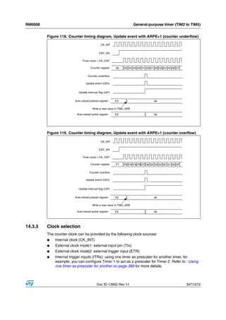
![General-purpose timer (TIM2 to TIM5) RM0008
Internal clock source (CK_INT)
If the slave mode controller is disabled (SMS=000 in the TIMx_SMCR register), then the
CEN, DIR (in the TIMx_CR1 register) and UG bits (in the TIMx_EGR register) are actual
control bits and can be changed only by software (except UG which remains cleared
automatically). As soon as the CEN bit is written to 1, the prescaler is clocked by the internal
clock CK_INT.
Figure 120 shows the behavior of the control circuit and the upcounter in normal mode,
without prescaler.
Figure 120. Control circuit in normal mode, internal clock divided by 1
CK_INT
CEN=CNT_EN
UG
CNT_INIT
Counter clock = CK_CNT = CK_PSC
COUNTER REGISTER 31 32 33 34 35 36 00 01 02 03 04 05 06 07
External clock source mode 1
This mode is selected when SMS=111 in the TIMx_SMCR register. The counter can count
at each rising or falling edge on a selected input.
Figure 121. TI2 external clock connection example
TIMx_SMCR
TS[2:0]
TI2F or
or
TI1F or encoder
ITRx 001 mode
TI1F_ED 100
TI1FP1 101 TRGI external clock
TI2F_Rising
mode 1 CK_PSC
0
TI2 Filter Edge TI2FP2 110
Detector TI2F_Falling ETRF external clock
1 ETRF 111 mode 2
ICF[3:0] CC2P CK_INT internal clock
TIMx_CCMR1 TIMx_CCER mode
(internal clock)
ECE SMS[2:0]
TIMx_SMCR
For example, to configure the upcounter to count in response to a rising edge on the TI2
input, use the following procedure:
For example, to configure the upcounter to count in response to a rising edge on the TI2
input, use the following procedure:
1. Configure channel 2 to detect rising edges on the TI2 input by writing CC2S= ‘01 in the
TIMx_CCMR1 register.
2. Configure the input filter duration by writing the IC2F[3:0] bits in the TIMx_CCMR1
register (if no filter is needed, keep IC2F=0000).
348/1072 Doc ID 13902 Rev 11](https://image.slidesharecdn.com/stm32referencemanual-110220082754-phpapp01/85/Stm32-reference-manual-348-320.jpg)
![RM0008 General-purpose timer (TIM2 to TIM5)
Note: The capture prescaler is not used for triggering, so you don’t need to configure it.
3. Select rising edge polarity by writing CC2P=0 in the TIMx_CCER register.
4. Configure the timer in external clock mode 1 by writing SMS=111 in the TIMx_SMCR
register.
5. Select TI2 as the input source by writing TS=110 in the TIMx_SMCR register.
6. Enable the counter by writing CEN=1 in the TIMx_CR1 register.
When a rising edge occurs on TI2, the counter counts once and the TIF flag is set.
The delay between the rising edge on TI2 and the actual clock of the counter is due to the
resynchronization circuit on TI2 input.
Figure 122. Control circuit in external clock mode 1
TI2
CNT_EN
Counter clock = CK_CNT = CK_PSC
Counter register 34 35 36
TIF
Write TIF=0
External clock source mode 2
This mode is selected by writing ECE=1 in the TIMx_SMCR register.
The counter can count at each rising or falling edge on the external trigger input ETR.
The Figure 123 gives an overview of the external trigger input block.
Figure 123. External trigger input block
TI2F or
or
TI1F or encoder
mode
TRGI external clock
mode 1 CK_PSC
ETR
ETR pin 0 ETRP
divider filter ETRF external clock
downcounter mode 2
/1, /2, /4, /8
1 CK_INT
CK_INT internal clock
mode
(internal clock)
ETP ETPS[1:0] ETF[3:0]
TIMx_SMCR TIMx_SMCR TIMx_SMCR ECE SMS[2:0]
TIMx_SMCR
For example, to configure the upcounter to count each 2 rising edges on ETR, use the
following procedure:
Doc ID 13902 Rev 11 349/1072](https://image.slidesharecdn.com/stm32referencemanual-110220082754-phpapp01/85/Stm32-reference-manual-349-320.jpg)
![General-purpose timer (TIM2 to TIM5) RM0008
1. As no filter is needed in this example, write ETF[3:0]=0000 in the TIMx_SMCR register.
2. Set the prescaler by writing ETPS[1:0]=01 in the TIMx_SMCR register
3. Select rising edge detection on the ETR pin by writing ETP=0 in the TIMx_SMCR
register
4. Enable external clock mode 2 by writing ECE=1 in the TIMx_SMCR register.
5. Enable the counter by writing CEN=1 in the TIMx_CR1 register.
The counter counts once each 2 ETR rising edges.
The delay between the rising edge on ETR and the actual clock of the counter is due to the
resynchronization circuit on the ETRP signal.
Figure 124. Control circuit in external clock mode 2
fMASTER
CNT_EN
ETR
ETRP
ETRF
Counter clock = CK_CNT = CK_PSC
Counter register 34 35 36
14.3.4 Capture/compare channels
Each Capture/Compare channel is built around a capture/compare register (including a
shadow register), a input stage for capture (with digital filter, multiplexing and prescaler) and
an output stage (with comparator and output control).
The following figure gives an overview of one Capture/Compare channel.
The input stage samples the corresponding TIx input to generate a filtered signal TIxF.
Then, an edge detector with polarity selection generates a signal (TIxFPx) which can be
used as trigger input by the slave mode controller or as the capture command. It is
prescaled before the capture register (ICxPS).
Figure 125. Capture/compare channel (example: channel 1 input stage)
TI1F_ED
to the slave mode controller
TI1F_Rising 0
TI1 TI1F
filter Edge TI1FP1
01
fDTS downcounter Detector TI1F_Falling
1
TI2FP1 IC1 divider IC1PS
10
/1, /2, /4, /8
ICF[3:0] CC1P TRC
11
TIMx_CCMR1 TIMx_CCER (from slave mode
controller)
TI2F_rising 0
(from channel 2)
CC1S[1:0] ICPS[1:0] CC1E
TI2F_falling
1
(from channel 2) TIMx_CCMR1 TIMx_CCER
350/1072 Doc ID 13902 Rev 11](https://image.slidesharecdn.com/stm32referencemanual-110220082754-phpapp01/85/Stm32-reference-manual-350-320.jpg)
![RM0008 General-purpose timer (TIM2 to TIM5)
The output stage generates an intermediate waveform which is then used for reference:
OCxRef (active high). The polarity acts at the end of the chain.
Figure 126. Capture/compare channel 1 main circuit
APB Bus
MCU-peripheral interface
(if 16-bit)
8 8
high
low
S write CCR1H
read CCR1H S write_in_progress
read_in_progress
Capture/Compare Preload Register write CCR1L
read CCR1L R
R CC1S[1]
output
capture_transfer compare_transfer mode
CC1S[0]
CC1S[1] input
mode OC1PE
Capture/Compare Shadow Register OC1PE
CC1S[0] UEV
TIMx_CCMR1
comparator (from time
IC1PS capture base unit)
CC1E CNT>CCR1
Counter
CNT=CCR1
CC1G
TIMx_EGR
Figure 127. Output stage of capture/compare channel (channel 1)
ETRF To the master mode 0
controller Output OC1
Enable
1 Circuit
CC1P
CNT > CCR1
Output mode oc1ref TIMx_CCER
CNT = CCR1 controller
CC1E TIMx_CCER
OC1M[2:0]
TIMx_CCMR1
The capture/compare block is made of one preload register and one shadow register. Write
and read always access the preload register.
In capture mode, captures are actually done in the shadow register, which is copied into the
preload register.
In compare mode, the content of the preload register is copied into the shadow register
which is compared to the counter.
Doc ID 13902 Rev 11 351/1072](https://image.slidesharecdn.com/stm32referencemanual-110220082754-phpapp01/85/Stm32-reference-manual-351-320.jpg)


![RM0008 General-purpose timer (TIM2 to TIM5)
The OPM waveform is defined by writing the compare registers (taking into account the
clock frequency and the counter prescaler).
● The tDELAY is defined by the value written in the TIMx_CCR1 register.
● The tPULSE is defined by the difference between the auto-reload value and the compare
value (TIMx_ARR - TIMx_CCR1).
● Let’s say you want to build a waveform with a transition from ‘0 to ‘1 when a compare
match occurs and a transition from ‘1 to ‘0 when the counter reaches the auto-reload
value. To do this you enable PWM mode 2 by writing OC1M=111 in the TIMx_CCMR1
register. You can optionally enable the preload registers by writing OC1PE=1 in the
TIMx_CCMR1 register and ARPE in the TIMx_CR1 register. In this case you have to
write the compare value in the TIMx_CCR1 register, the auto-reload value in the
TIMx_ARR register, generate an update by setting the UG bit and wait for external
trigger event on TI2. CC1P is written to ‘0 in this example.
In our example, the DIR and CMS bits in the TIMx_CR1 register should be low.
You only want 1 pulse(Single mode), so you write '1 in the OPM bit in the TIMx_CR1 register
to stop the counter at the next update event (when the counter rolls over from the auto-
reload value back to 0). When OPM bit in the TIMx_CR1 register is set to '0', so the
Repetitive Mode is selected.
Particular case: OCx fast enable:
In One-pulse mode, the edge detection on TIx input set the CEN bit which enables the
counter. Then the comparison between the counter and the compare value makes the
output toggle. But several clock cycles are needed for these operations and it limits the
minimum delay tDELAY min we can get.
If you want to output a waveform with the minimum delay, you can set the OCxFE bit in the
TIMx_CCMRx register. Then OCxRef (and OCx) is forced in response to the stimulus,
without taking in account the comparison. Its new level is the same as if a compare match
had occurred. OCxFE acts only if the channel is configured in PWM1 or PWM2 mode.
14.3.11 Clearing the OCxREF signal on an external event
The OCxREF signal for a given channel can be reset by applying a high level on the ETRF
input (OCxCE enable bit set to 1 in the corresponding TIMx_CCMRx register). OCxREF
remains low until the next update event (UEV) occurs.
This function can be used only in the output compare and PWM modes. It does not work in
forced mode.
For example, the OCxREF signal can be connected to the output of a comparator to be used
for current handling. In this case, ETR must be configured as follows:
1. The external trigger prescaler should be kept off: bits ETPS[1:0] in the TIMx_SMCR
register are cleared to 00.
2. The external clock mode 2 must be disabled: bit ECE in the TIM1_SMCR register is
cleared to 0.
3. The external trigger polarity (ETP) and the external trigger filter (ETF) can be
configured according to the application’s needs.
Figure 133 shows the behavior of the OCxREF signal when the ETRF input becomes high,
for both values of the OCxCE enable bit. In this example, the timer TIMx is programmed in
PWM mode.
Doc ID 13902 Rev 11 359/1072](https://image.slidesharecdn.com/stm32referencemanual-110220082754-phpapp01/85/Stm32-reference-manual-359-320.jpg)


![RM0008 General-purpose timer (TIM2 to TIM5)
14.4 TIMx2 to TIM5 registers
Refer to Section 1.1 on page 40 for a list of abbreviations used in register descriptions.
The peripheral registers can be accessed by half-words (16-bit) or words (32-bit).
14.4.1 TIMx control register 1 (TIMx_CR1)
Address offset: 0x00
Reset value: 0x0000
15 14 13 12 11 10 9 8 7 6 5 4 3 2 1 0
CKD[1:0] ARPE CMS DIR OPM URS UDIS CEN
Reserved
rw rw rw rw rw rw rw rw rw rw
Bits 15:10 Reserved, always read as 0
Bits 9:8 CKD: Clock division
This bit-field indicates the division ratio between the timer clock (CK_INT) frequency and
sampling clock used by the digital filters (ETR, TIx),
00: tDTS = tCK_INT
01: tDTS = 2 × tCK_INT
10: tDTS = 4 × tCK_INT
11: Reserved
Bit 7 ARPE: Auto-reload preload enable
0: TIMx_ARR register is not buffered
1: TIMx_ARR register is buffered
Bits 6:5 CMS: Center-aligned mode selection
00: Edge-aligned mode. The counter counts up or down depending on the direction bit
(DIR).
01: Center-aligned mode 1. The counter counts up and down alternatively. Output compare
interrupt flags of channels configured in output (CCxS=00 in TIMx_CCMRx register) are set
only when the counter is counting down.
10: Center-aligned mode 2. The counter counts up and down alternatively. Output compare
interrupt flags of channels configured in output (CCxS=00 in TIMx_CCMRx register) are set
only when the counter is counting up.
11: Center-aligned mode 3. The counter counts up and down alternatively. Output compare
interrupt flags of channels configured in output (CCxS=00 in TIMx_CCMRx register) are set
both when the counter is counting up or down.
Note: It is not allowed to switch from edge-aligned mode to center-aligned mode as long as
the counter is enabled (CEN=1)
Bit 4 DIR: Direction
0: Counter used as upcounter
1: Counter used as downcounter
Note: This bit is read only when the timer is configured in Center-aligned mode or Encoder
mode.
Bit 3 OPM: One-pulse mode
0: Counter is not stopped at update event
1: Counter stops counting at the next update event (clearing the bit CEN)
Doc ID 13902 Rev 11 371/1072](https://image.slidesharecdn.com/stm32referencemanual-110220082754-phpapp01/85/Stm32-reference-manual-371-320.jpg)
![General-purpose timer (TIM2 to TIM5) RM0008
Bit 2 URS: Update request source
This bit is set and cleared by software to select the UEV event sources.
0: Any of the following events generate an update interrupt or DMA request if enabled.
These events can be:
– Counter overflow/underflow
– Setting the UG bit
– Update generation through the slave mode controller
1: Only counter overflow/underflow generates an update interrupt or DMA request if enabled.
Bit 1 UDIS: Update disable
This bit is set and cleared by software to enable/disable UEV event generation.
0: UEV enabled. The Update (UEV) event is generated by one of the following events:
– Counter overflow/underflow
– Setting the UG bit
– Update generation through the slave mode controller
Buffered registers are then loaded with their preload values.
1: UEV disabled. The Update event is not generated, shadow registers keep their value
(ARR, PSC, CCRx). However the counter and the prescaler are reinitialized if the UG bit is
set or if a hardware reset is received from the slave mode controller.
Bit 0 CEN: Counter enable
0: Counter disabled
1: Counter enabled
Note: External clock, gated mode and encoder mode can work only if the CEN bit has been
previously set by software. However trigger mode can set the CEN bit automatically by
hardware.
CEN is cleared automatically in one-pulse mode, when an update event occurs.
14.4.2 TIMx control register 2 (TIMx_CR2)
Address offset: 0x04
Reset value: 0x0000
15 14 13 12 11 10 9 8 7 6 5 4 3 2 1 0
TI1S MMS[2:0] CCDS
Reserved Reserved
rw rw rw rw rw
Bits 15:8 Reserved, always read as 0.
Bit 7 TI1S: TI1 selection
0: The TIMx_CH1 pin is connected to TI1 input
1: The TIMx_CH1, CH2 and CH3 pins are connected to the TI1 input (XOR combination)
See also Section 13.3.18: Interfacing with Hall sensors on page 304
372/1072 Doc ID 13902 Rev 11](https://image.slidesharecdn.com/stm32referencemanual-110220082754-phpapp01/85/Stm32-reference-manual-372-320.jpg)
![RM0008 General-purpose timer (TIM2 to TIM5)
Bits 6:4 MMS: Master mode selection
These bits allow to select the information to be sent in master mode to slave timers for
synchronization (TRGO). The combination is as follows:
000: Reset - the UG bit from the TIMx_EGR register is used as trigger output (TRGO). If the
reset is generated by the trigger input (slave mode controller configured in reset mode) then
the signal on TRGO is delayed compared to the actual reset.
001: Enable - the Counter enable signal, CNT_EN, is used as trigger output (TRGO). It is
useful to start several timers at the same time or to control a window in which a slave timer is
enabled. The Counter Enable signal is generated by a logic OR between CEN control bit and
the trigger input when configured in gated mode.
When the Counter Enable signal is controlled by the trigger input, there is a delay on TRGO,
except if the master/slave mode is selected (see the MSM bit description in TIMx_SMCR
register).
010: Update - The update event is selected as trigger output (TRGO). For instance a master
timer can then be used as a prescaler for a slave timer.
011: Compare Pulse - The trigger output send a positive pulse when the CC1IF flag is to be
set (even if it was already high), as soon as a capture or a compare match occurred. (TRGO)
100: Compare - OC1REF signal is used as trigger output (TRGO)
101: Compare - OC2REF signal is used as trigger output (TRGO)
110: Compare - OC3REF signal is used as trigger output (TRGO)
111: Compare - OC4REF signal is used as trigger output (TRGO)
Bit 3 CCDS: Capture/compare DMA selection
0: CCx DMA request sent when CCx event occurs
1: CCx DMA requests sent when update event occurs
Bits 2:0 Reserved, always read as 0
14.4.3 TIMx slave mode control register (TIMx_SMCR)
Address offset: 0x08
Reset value: 0x0000
15 14 13 12 11 10 9 8 7 6 5 4 3 2 1 0
ETP ECE ETPS[1:0] ETF[3:0] MSM TS[2:0] SMS[2:0]
Res.
rw rw rw rw rw rw rw rw rw rw rw rw rw rw rw
Bit 15 ETP: External trigger polarity
This bit selects whether ETR or ETR is used for trigger operations
0: ETR is non-inverted, active at high level or rising edge
1: ETR is inverted, active at low level or falling edge
Bit 14 ECE: External clock enable
This bit enables External clock mode 2.
0: External clock mode 2 disabled
1: External clock mode 2 enabled. The counter is clocked by any active edge on the ETRF
signal.
1: Setting the ECE bit has the same effect as selecting external clock mode 1 with TRGI
connected to ETRF (SMS=111 and TS=111).
2: It is possible to simultaneously use external clock mode 2 with the following slave modes:
reset mode, gated mode and trigger mode. Nevertheless, TRGI must not be connected to
ETRF in this case (TS bits must not be 111).
3: If external clock mode 1 and external clock mode 2 are enabled at the same time, the
external clock input is ETRF.
Doc ID 13902 Rev 11 373/1072](https://image.slidesharecdn.com/stm32referencemanual-110220082754-phpapp01/85/Stm32-reference-manual-373-320.jpg)
![General-purpose timer (TIM2 to TIM5) RM0008
Bits 13:12 ETPS: External trigger prescaler
External trigger signal ETRP frequency must be at most 1/4 of CK_INT frequency. A
prescaler can be enabled to reduce ETRP frequency. It is useful when inputting fast external
clocks.
00: Prescaler OFF
01: ETRP frequency divided by 2
10: ETRP frequency divided by 4
11: ETRP frequency divided by 8
Bits 11:8 ETF[3:0]: External trigger filter
This bit-field then defines the frequency used to sample ETRP signal and the length of the
digital filter applied to ETRP. The digital filter is made of an event counter in which N events
are needed to validate a transition on the output:
0000: No filter, sampling is done at fDTS
0001: fSAMPLING=fCK_INT, N=2
0010: fSAMPLING=fCK_INT, N=4
0011: fSAMPLING=fCK_INT, N=8
0100: fSAMPLING=fDTS/2, N=6
0101: fSAMPLING=fDTS/2, N=8
0110: fSAMPLING=fDTS/4, N=6
0111: fSAMPLING=fDTS/4, N=8
1000: fSAMPLING=fDTS/8, N=6
1001: fSAMPLING=fDTS/8, N=8
1010: fSAMPLING=fDTS/16, N=5
1011: fSAMPLING=fDTS/16, N=6
1100: fSAMPLING=fDTS/16, N=8
1101: fSAMPLING=fDTS/32, N=5
1110: fSAMPLING=fDTS/32, N=6
1111: fSAMPLING=fDTS/32, N=8
Bit 7 MSM: Master/Slave mode
0: No action
1: The effect of an event on the trigger input (TRGI) is delayed to allow a perfect
synchronization between the current timer and its slaves (through TRGO). It is useful if we
want to synchronize several timers on a single external event.
Bits 6:4 TS: Trigger selection
This bit-field selects the trigger input to be used to synchronize the counter.
000: Internal Trigger 0 (ITR0).
001: Internal Trigger 1 (ITR1).
010: Internal Trigger 2 (ITR2).
011: Internal Trigger 3 (ITR3).
100: TI1 Edge Detector (TI1F_ED)
101: Filtered Timer Input 1 (TI1FP1)
110: Filtered Timer Input 2 (TI2FP2)
111: External Trigger input (ETRF)
See Table 84: TIMx Internal trigger connection on page 375 for more details on ITRx
meaning for each Timer.
Note: These bits must be changed only when they are not used (e.g. when SMS=000) to
avoid wrong edge detections at the transition.
Bit 3 Reserved, always read as 0.
374/1072 Doc ID 13902 Rev 11](https://image.slidesharecdn.com/stm32referencemanual-110220082754-phpapp01/85/Stm32-reference-manual-374-320.jpg)


![RM0008 General-purpose timer (TIM2 to TIM5)
Bit 2 CC2G: Capture/compare 2 generation
refer to CC1G description
Bit 1 CC1G: Capture/compare 1 generation
This bit is set by software in order to generate an event, it is automatically cleared by
hardware.
0: No action
1: A capture/compare event is generated on channel 1:
If channel CC1 is configured as output:
CC1IF flag is set, Corresponding interrupt or DMA request is sent if enabled.
If channel CC1 is configured as input:
The current value of the counter is captured in TIMx_CCR1 register. The CC1IF flag is set,
the corresponding interrupt or DMA request is sent if enabled. The CC1OF flag is set if the
CC1IF flag was already high.
Bit 0 UG: Update generation
This bit can be set by software, it is automatically cleared by hardware.
0: No action
1: Re-initialize the counter and generates an update of the registers. Note that the prescaler
counter is cleared too (anyway the prescaler ratio is not affected). The counter is cleared if
the center-aligned mode is selected or if DIR=0 (upcounting), else it takes the auto-reload
value (TIMx_ARR) if DIR=1 (downcounting).
14.4.7 TIMx capture/compare mode register 1 (TIMx_CCMR1)
Address offset: 0x18
Reset value: 0x0000
The channels can be used in input (capture mode) or in output (compare mode). The
direction of a channel is defined by configuring the corresponding CCxS bits. All the other
bits of this register have a different function in input and in output mode. For a given bit,
OCxx describes its function when the channel is configured in output, ICxx describes its
function when the channel is configured in input. So you must take care that the same bit
can have a different meaning for the input stage and for the output stage.
15 14 13 12 11 10 9 8 7 6 5 4 3 2 1 0
OC2CE OC2M[2:0] OC2PE OC2FE OC1CE OC1M[2:0] OC1PE OC1FE
CC2S[1:0] CC1S[1:0]
IC2F[3:0] IC2PSC[1:0] IC1F[3:0] IC1PSC[1:0]
rw rw rw rw rw rw rw rw rw rw rw rw rw rw rw rw
Output compare mode
Bit 15 OC2CE: Output compare 2 clear enable
Bits 14:12 OC2M[2:0]: Output compare 2 mode
Bit 11 OC2PE: Output compare 2 preload enable
Bit 10 OC2FE: Output compare 2 fast enable
Doc ID 13902 Rev 11 379/1072](https://image.slidesharecdn.com/stm32referencemanual-110220082754-phpapp01/85/Stm32-reference-manual-379-320.jpg)
![General-purpose timer (TIM2 to TIM5) RM0008
Bits 9:8 CC2S[1:0]: Capture/Compare 2 selection
This bit-field defines the direction of the channel (input/output) as well as the used input.
00: CC2 channel is configured as output
01: CC2 channel is configured as input, IC2 is mapped on TI2
10: CC2 channel is configured as input, IC2 is mapped on TI1
11: CC2 channel is configured as input, IC2 is mapped on TRC. This mode is working only
if an internal trigger input is selected through the TS bit (TIMx_SMCR register)
Note: CC2S bits are writable only when the channel is OFF (CC2E = 0 in TIMx_CCER).
Bit 7 OC1CE: Output compare 1 clear enable
OC1CE: Output Compare 1 Clear Enable
0: OC1Ref is not affected by the ETRF input
1: OC1Ref is cleared as soon as a High level is detected on ETRF input
Bits 6:4 OC1M: Output compare 1 mode
These bits define the behavior of the output reference signal OC1REF from which OC1 and
OC1N are derived. OC1REF is active high whereas OC1 and OC1N active level depends
on CC1P and CC1NP bits.
000: Frozen - The comparison between the output compare register TIMx_CCR1 and the
counter TIMx_CNT has no effect on the outputs.(this mode is used to generate a timing
base).
001: Set channel 1 to active level on match. OC1REF signal is forced high when the counter
TIMx_CNT matches the capture/compare register 1 (TIMx_CCR1).
010: Set channel 1 to inactive level on match. OC1REF signal is forced low when the
counter TIMx_CNT matches the capture/compare register 1 (TIMx_CCR1).
011: Toggle - OC1REF toggles when TIMx_CNT=TIMx_CCR1.
100: Force inactive level - OC1REF is forced low.
101: Force active level - OC1REF is forced high.
110: PWM mode 1 - In upcounting, channel 1 is active as long as TIMx_CNT<TIMx_CCR1
else inactive. In downcounting, channel 1 is inactive (OC1REF=‘0) as long as
TIMx_CNT>TIMx_CCR1 else active (OC1REF=1).
111: PWM mode 2 - In upcounting, channel 1 is inactive as long as
TIMx_CNT<TIMx_CCR1 else active. In downcounting, channel 1 is active as long as
TIMx_CNT>TIMx_CCR1 else inactive.
Note: 1: These bits can not be modified as long as LOCK level 3 has been programmed
(LOCK bits in TIMx_BDTR register) and CC1S=00 (the channel is configured in
output).
2: In PWM mode 1 or 2, the OCREF level changes only when the result of the
comparison changes or when the output compare mode switches from “frozen” mode
to “PWM” mode.
Bit 3 OC1PE: Output compare 1 preload enable
0: Preload register on TIMx_CCR1 disabled. TIMx_CCR1 can be written at anytime, the
new value is taken in account immediately.
1: Preload register on TIMx_CCR1 enabled. Read/Write operations access the preload
register. TIMx_CCR1 preload value is loaded in the active register at each update event.
Note: 1: These bits can not be modified as long as LOCK level 3 has been programmed
(LOCK bits in TIMx_BDTR register) and CC1S=00 (the channel is configured in
output).
2: The PWM mode can be used without validating the preload register only in one-
pulse mode (OPM bit set in TIMx_CR1 register). Else the behavior is not guaranteed.
380/1072 Doc ID 13902 Rev 11](https://image.slidesharecdn.com/stm32referencemanual-110220082754-phpapp01/85/Stm32-reference-manual-380-320.jpg)
![RM0008 General-purpose timer (TIM2 to TIM5)
Bit 2 OC1FE: Output compare 1 fast enable
This bit is used to accelerate the effect of an event on the trigger in input on the CC output.
0: CC1 behaves normally depending on counter and CCR1 values even when the trigger is
ON. The minimum delay to activate CC1 output when an edge occurs on the trigger input is
5 clock cycles.
1: An active edge on the trigger input acts like a compare match on CC1 output. Then, OC
is set to the compare level independently from the result of the comparison. Delay to sample
the trigger input and to activate CC1 output is reduced to 3 clock cycles. OCFE acts only if
the channel is configured in PWM1 or PWM2 mode.
Bits 1:0 CC1S: Capture/Compare 1 selection
This bit-field defines the direction of the channel (input/output) as well as the used input.
00: CC1 channel is configured as output.
01: CC1 channel is configured as input, IC1 is mapped on TI1.
10: CC1 channel is configured as input, IC1 is mapped on TI2.
11: CC1 channel is configured as input, IC1 is mapped on TRC. This mode is working only
if an internal trigger input is selected through TS bit (TIMx_SMCR register)
Note: CC1S bits are writable only when the channel is OFF (CC1E = 0 in TIMx_CCER).
Input capture mode
Bits 15:12 IC2F: Input capture 2 filter
Bits 11:10 IC2PSC[1:0]: Input capture 2 prescaler
Bits 9:8 CC2S: Capture/compare 2 selection
This bit-field defines the direction of the channel (input/output) as well as the used input.
00: CC2 channel is configured as output.
01: CC2 channel is configured as input, IC2 is mapped on TI2.
10: CC2 channel is configured as input, IC2 is mapped on TI1.
11: CC2 channel is configured as input, IC2 is mapped on TRC. This mode is working only if
an internal trigger input is selected through TS bit (TIMx_SMCR register)
Note: CC2S bits are writable only when the channel is OFF (CC2E = 0 in TIMx_CCER).
Doc ID 13902 Rev 11 381/1072](https://image.slidesharecdn.com/stm32referencemanual-110220082754-phpapp01/85/Stm32-reference-manual-381-320.jpg)
![General-purpose timer (TIM2 to TIM5) RM0008
Bits 7:4 IC1F: Input capture 1 filter
This bit-field defines the frequency used to sample TI1 input and the length of the digital filter
applied to TI1. The digital filter is made of an event counter in which N events are needed to
validate a transition on the output:
0000: No filter, sampling is done at fDTS
0001: fSAMPLING=fCK_INT, N=2
0010: fSAMPLING=fCK_INT, N=4
0011: fSAMPLING=fCK_INT, N=8
0100: fSAMPLING=fDTS/2, N=6
0101: fSAMPLING=fDTS/2, N=8
0110: fSAMPLING=fDTS/4, N=6
0111: fSAMPLING=fDTS/4, N=8
1000: fSAMPLING=fDTS/8, N=6
1001: fSAMPLING=fDTS/8, N=8
1010: fSAMPLING=fDTS/16, N=5
1011: fSAMPLING=fDTS/16, N=6
1100: fSAMPLING=fDTS/16, N=8
1101: fSAMPLING=fDTS/32, N=5
1110: fSAMPLING=fDTS/32, N=6
1111: fSAMPLING=fDTS/32, N=8
Note: In current silicon revision, fDTS is replaced in the formula by CK_INT when ICxF[3:0]= 1,
2 or 3.
Bits 3:2 IC1PSC: Input capture 1 prescaler
This bit-field defines the ratio of the prescaler acting on CC1 input (IC1).
The prescaler is reset as soon as CC1E=0 (TIMx_CCER register).
00: no prescaler, capture is done each time an edge is detected on the capture input
01: capture is done once every 2 events
10: capture is done once every 4 events
11: capture is done once every 8 events
Bits 1:0 CC1S: Capture/Compare 1 selection
This bit-field defines the direction of the channel (input/output) as well as the used input.
00: CC1 channel is configured as output
01: CC1 channel is configured as input, IC1 is mapped on TI1
10: CC1 channel is configured as input, IC1 is mapped on TI2
11: CC1 channel is configured as input, IC1 is mapped on TRC. This mode is working only if
an internal trigger input is selected through TS bit (TIMx_SMCR register)
Note: CC1S bits are writable only when the channel is OFF (CC1E = 0 in TIMx_CCER).
382/1072 Doc ID 13902 Rev 11](https://image.slidesharecdn.com/stm32referencemanual-110220082754-phpapp01/85/Stm32-reference-manual-382-320.jpg)
![RM0008 General-purpose timer (TIM2 to TIM5)
14.4.8 Capture/compare mode register 2 (TIMx_CCMR2)
Address offset: 0x1C
Reset value: 0x0000
Refer to the above CCMR1 register description.
15 14 13 12 11 10 9 8 7 6 5 4 3 2 1 0
OC4CE OC4M[2:0] OC4PE OC4FE OC3CE OC3M[2:0] OC3PE OC3FE
CC4S[1:0] CC3S[1:0]
IC4F[3:0] IC4PSC[1:0] IC3F[3:0] IC3PSC[1:0]
rw rw rw rw rw rw rw rw rw rw rw rw rw rw rw rw
Output compare mode
Bit 15 OC4CE: Output compare 4 clear enable
Bits 14:12 OC4M: Output compare 4 mode
Bit 11 OC4PE: Output compare 4 preload enable
Bit 10 OC4FE: Output compare 4 fast enable
Bits 9:8 CC4S: Capture/Compare 4 selection
This bit-field defines the direction of the channel (input/output) as well as the used input.
00: CC4 channel is configured as output
01: CC4 channel is configured as input, IC4 is mapped on TI4
10: CC4 channel is configured as input, IC4 is mapped on TI3
11: CC4 channel is configured as input, IC4 is mapped on TRC. This mode is working only if
an internal trigger input is selected through TS bit (TIMx_SMCR register)
Note: CC4S bits are writable only when the channel is OFF (CC4E = 0 in TIMx_CCER).
Bit 7 OC3CE: Output compare 3 clear enable
Bits 6:4 OC3M: Output compare 3 mode
Bit 3 OC3PE: Output compare 3 preload enable
Bit 2 OC3FE: Output compare 3 fast enable
Bits 1:0 CC3S: Capture/Compare 3 selection
This bit-field defines the direction of the channel (input/output) as well as the used input.
00: CC3 channel is configured as output
01: CC3 channel is configured as input, IC3 is mapped on TI3
10: CC3 channel is configured as input, IC3 is mapped on TI4
11: CC3 channel is configured as input, IC3 is mapped on TRC. This mode is working only if
an internal trigger input is selected through TS bit (TIMx_SMCR register)
Note: CC3S bits are writable only when the channel is OFF (CC3E = 0 in TIMx_CCER).
Doc ID 13902 Rev 11 383/1072](https://image.slidesharecdn.com/stm32referencemanual-110220082754-phpapp01/85/Stm32-reference-manual-383-320.jpg)

![RM0008 General-purpose timer (TIM2 to TIM5)
Bit 4 CC2E: Capture/Compare 2 output enable
refer to CC1E description
Bits 3:2 Reserved, always read as 0.
Bit 1 CC1P: Capture/Compare 1 output polarity
CC1 channel configured as output:
0: OC1 active high.
1: OC1 active low.
CC1 channel configured as input:
This bit selects whether IC1 or IC1 is used for trigger or capture operations.
0: non-inverted: capture is done on a rising edge of IC1. When used as external trigger, IC1
is non-inverted.
1: inverted: capture is done on a falling edge of IC1. When used as external trigger, IC1 is
inverted.
Bit 0 CC1E: Capture/Compare 1 output enable
CC1 channel configured as output:
0: Off - OC1 is not active.
1: On - OC1 signal is output on the corresponding output pin.
CC1 channel configured as input:
This bit determines if a capture of the counter value can actually be done into the input
capture/compare register 1 (TIMx_CCR1) or not.
0: Capture disabled.
1: Capture enabled.
Table 85. Output control bit for standard OCx channels
CCxE bit OCx output state
0 Output Disabled (OCx=0, OCx_EN=0)
1 OCx=OCxREF + Polarity, OCx_EN=1
Note: The state of the external IO pins connected to the standard OCx channels depends on the
OCx channel state and the GPIO and AFIO registers.
14.4.10 TIMx counter (TIMx_CNT)
Address offset: 0x24
Reset value: 0x0000
15 14 13 12 11 10 9 8 7 6 5 4 3 2 1 0
CNT[15:0]
rw rw rw rw rw rw rw rw rw rw rw rw rw rw rw rw
Bits 15:0 CNT[15:0]: Counter value
Doc ID 13902 Rev 11 385/1072](https://image.slidesharecdn.com/stm32referencemanual-110220082754-phpapp01/85/Stm32-reference-manual-385-320.jpg)
![General-purpose timer (TIM2 to TIM5) RM0008
14.4.11 TIMx prescaler (TIMx_PSC)
Address offset: 0x28
Reset value: 0x0000
15 14 13 12 11 10 9 8 7 6 5 4 3 2 1 0
PSC[15:0]
rw rw rw rw rw rw rw rw rw rw rw rw rw rw rw rw
Bits 15:0 PSC[15:0]: Prescaler value
The counter clock frequency CK_CNT is equal to fCK_PSC / (PSC[15:0] + 1).
PSC contains the value to be loaded in the active prescaler register at each update event.
14.4.12 TIMx auto-reload register (TIMx_ARR)
Address offset: 0x2C
Reset value: 0x0000
15 14 13 12 11 10 9 8 7 6 5 4 3 2 1 0
ARR[15:0]
rw rw rw rw rw rw rw rw rw rw rw rw rw rw rw rw
Bits 15:0 ARR[15:0]: Prescaler value
ARR is the value to be loaded in the actual auto-reload register.
Refer to the Section 14.3.1: Time-base unit on page 337 for more details about ARR update
and behavior.
The counter is blocked while the auto-reload value is null.
14.4.13 TIMx capture/compare register 1 (TIMx_CCR1)
Address offset: 0x34
Reset value: 0x0000
15 14 13 12 11 10 9 8 7 6 5 4 3 2 1 0
CCR1[15:0]
rw rw rw rw rw rw rw rw rw rw rw rw rw rw rw rw
Bits 15:0 CCR1[15:0]: Capture/Compare 1 value
If channel CC1 is configured as output:
CCR1 is the value to be loaded in the actual capture/compare 1 register (preload value).
It is loaded permanently if the preload feature is not selected in the TIMx_CCMR1 register (bit
OC1PE). Else the preload value is copied in the active capture/compare 1 register when an
update event occurs.
The active capture/compare register contains the value to be compared to the counter
TIMx_CNT and signaled on OC1 output.
If channel CC1is configured as input:
CCR1 is the counter value transferred by the last input capture 1 event (IC1).
386/1072 Doc ID 13902 Rev 11](https://image.slidesharecdn.com/stm32referencemanual-110220082754-phpapp01/85/Stm32-reference-manual-386-320.jpg)
![RM0008 General-purpose timer (TIM2 to TIM5)
14.4.14 TIMx capture/compare register 2 (TIMx_CCR2)
Address offset: 0x38
Reset value: 0x0000
15 14 13 12 11 10 9 8 7 6 5 4 3 2 1 0
CCR2[15:0]
rw rw rw rw rw rw rw rw rw rw rw rw rw rw rw rw
Bits 15:0 CCR2[15:0]: Capture/Compare 2 value
If channel CC2 is configured as output:
CCR2 is the value to be loaded in the actual capture/compare 2 register (preload value).
It is loaded permanently if the preload feature is not selected in the TIMx_CCMR2 register
(bit OC2PE). Else the preload value is copied in the active capture/compare 2 register when
an update event occurs.
The active capture/compare register contains the value to be compared to the counter
TIMx_CNT and signalled on OC2 output.
If channel CC2 is configured as input:
CCR2 is the counter value transferred by the last input capture 2 event (IC2).
14.4.15 TIMx capture/compare register 3 (TIMx_CCR3)
Address offset: 0x3C
Reset value: 0x0000
15 14 13 12 11 10 9 8 7 6 5 4 3 2 1 0
CCR3[15:0]
rw rw rw rw rw rw rw rw rw rw rw rw rw rw rw rw
Bits 15:0 CCR3[15:0]: Capture/Compare value
If channel CC3 is configured as output:
CCR3 is the value to be loaded in the actual capture/compare 3 register (preload value).
It is loaded permanently if the preload feature is not selected in the TIMx_CCMR3 register
(bit OC3PE). Else the preload value is copied in the active capture/compare 3 register when
an update event occurs.
The active capture/compare register contains the value to be compared to the counter
TIMx_CNT and signalled on OC3 output.
If channel CC3is configured as input:
CCR3 is the counter value transferred by the last input capture 3 event (IC3).
Doc ID 13902 Rev 11 387/1072](https://image.slidesharecdn.com/stm32referencemanual-110220082754-phpapp01/85/Stm32-reference-manual-387-320.jpg)
![General-purpose timer (TIM2 to TIM5) RM0008
14.4.16 TIMx capture/compare register 4 (TIMx_CCR4)
Address offset: 0x40
Reset value: 0x0000
15 14 13 12 11 10 9 8 7 6 5 4 3 2 1 0
CCR4[15:0]
rw rw rw rw rw rw rw rw rw rw rw rw rw rw rw rw
Bits 15:0 CCR4[15:0]: Capture/Compare value
1/ if CC4 channel is configured as output (CC4S bits):
CCR4 is the value to be loaded in the actual capture/compare 4 register (preload value).
It is loaded permanently if the preload feature is not selected in the TIMx_CCMR4 register (bit
OC4PE). Else the preload value is copied in the active capture/compare 4 register when an
update event occurs.
The active capture/compare register contains the value to be compared to the counter
TIMx_CNT and signalled on OC4 output.
2/ if CC4 channel is configured as input (CC4S bits in TIMx_CCMR4 register):
CCR4 is the counter value transferred by the last input capture 4 event (IC4).
14.4.17 TIMx DMA control register (TIMx_DCR)
Address offset: 0x48
Reset value: 0x0000
15 14 13 12 11 10 9 8 7 6 5 4 3 2 1 0
DBL[4:0] DBA[4:0]
Reserved Reserved
rw rw rw rw rw rw rw rw rw rw
Bits 15:13 Reserved, always read as 0
Bits 12:8 DBL[4:0]: DMA burst length
This 5-bits vector defines the length of DMA transfers (the timer recognizes a burst transfer
when a read or a write access is done to the TIMx_DMAR address), i.e. the number of bytes to
be transferred.
00000: 1 byte,
00001: 2 bytes,
00010: 3 bytes,
...
10001: 18 bytes.
Bits 7:5 Reserved, always read as 0
Bits 4:0 DBA[4:0]: DMA base address
This 5-bit vector defines the base-address for DMA transfers (when read/write access are
done through the TIMx_DMAR address). DBA is defined as an offset starting from the
address of the TIMx_CR1 register.
Example:
00000: TIMx_CR1,
00001: TIMx_CR2,
00010: TIMx_SMCR,
...
388/1072 Doc ID 13902 Rev 11](https://image.slidesharecdn.com/stm32referencemanual-110220082754-phpapp01/85/Stm32-reference-manual-388-320.jpg)
![RM0008 General-purpose timer (TIM2 to TIM5)
14.4.18 TIMx DMA address for full transfer (TIMx_DMAR)
Address offset: 0x4C
Reset value: 0x0000
15 14 13 12 11 10 9 8 7 6 5 4 3 2 1 0
DMAB[15:0]
rw rw rw rw rw rw rw rw rw rw rw rw rw rw rw rw
Bits 15:0 DMAB[15:0]: DMA register for burst accesses
A read or write access to the DMAR register accesses the register located at the address:
“(TIMx_CR1 address) + DBA + (DMA index)” in which:
TIMx_CR1 address is the address of the control register 1,
DBA is the DMA base address configured in the TIMx_DCR register,
DMA index is the offset automatically controlled by the DMA transfer, depending on the
length of the transfer DBL in the TIMx_DCR register.
14.4.19 TIMx register map
TIMx registers are mapped as 16-bit addressable registers as described in the table below:
Table 86. TIMx register map and reset values
31
30
29
28
27
26
25
24
23
22
21
20
19
18
17
16
15
14
13
12
11
10
Offset Register
9
8
7
6
5
4
3
2
1
0
ARPE
UDIS
OPM
CKD CMS
CEN
URS
DIR
TIMx_CR1
0x00 Reserved [1:0] [1:0]
Reset value 0 0 0 0 0 0 0 0 0 0
CCDS
TI1S
TIMx_CR2 MMS[2:0]
0x04 Reserved Reserved
Reset value 0 0 0 0 0
CC3IE Reserved
MSM
ETPS
ECE
ETP
TIMx_SMCR ETF[3:0] TS[2:0] SMS[2:0]
0x08 Reserved [1:0]
Reset value 0 0 0 0 0 0 0 0 0 0 0 0 0 0 0
COMDE
CC4DE
CC3DE
CC2DE
CC1DE
Reserved
Reserved Reserved Reserved
CC4IE
CC2IE
CC1IE
UDE
TDE
UIE
TIE
TIMx_DIER
0x0C Reserved
Reset value 0 0 0 0 0 0 0 0 0 0 0 0 0
CC4OF
CC3OF
CC2OF
CC1OF
Reserved
CC4IF
CC3IF
CC2IF
CC1IF
UIF
TIF
TIMx_SR
0x10 Reserved
Reset value 0 0 0 0 0 0 0 0 0 0
CC4G
CC3G
CC2G
CC1G
UG
TG
TIMx_EGR
0x14 Reserved
Reset value 0 0 0 0 0 0
TIMx_CCMR1
OC2CE
OC1CE
OC2PE
OC1PE
OC2FE
OC1FE
OC2M CC2S OC1M CC1S
Output Compare [2:0] [1:0] [2:0] [1:0]
Reserved
mode
Reset value 0 0 0 0 0 0 0 0 0 0 0 0 0 0 0 0
0x18
TIMx_CCMR1 IC2 IC1
CC2S CC1S
Input Capture IC2F[3:0] PSC IC1F[3:0] PSC
Reserved [1:0] [1:0]
mode [1:0] [1:0]
Reset value 0 0 0 0 0 0 0 0 0 0 0 0 0 0 0 0
Doc ID 13902 Rev 11 389/1072](https://image.slidesharecdn.com/stm32referencemanual-110220082754-phpapp01/85/Stm32-reference-manual-389-320.jpg)
![General-purpose timer (TIM2 to TIM5) RM0008
Table 86. TIMx register map and reset values (continued)
31
30
29
28
27
26
25
24
23
22
21
20
19
18
17
16
15
14
13
12
11
10
Offset Register
9
8
7
6
5
4
3
2
1
0
TIMx_CCMR2
OC3CE
OC4PE
OC3PE
OC4FE
OC3FE
O24CE
OC4M CC4S OC3M CC3S
Output Compare
Reserved [2:0] [1:0] [2:0] [1:0]
mode
Reset value 0 0 0 0 0 0 0 0 0 0 0 0 0 0 0 0
0x1C
TIMx_CCMR2 IC4 IC3
CC4S CC3S
Input Capture IC4F[3:0] PSC IC3F[3:0] PSC
Reserved [1:0] [1:0]
mode [1:0] [1:0]
Reset value 0 0 0 0 0 0 0 0 0 0 0 0 0 0 0 0
Reserved
Reserved
Reserved
CC4P
CC4E
CC3P
CC3E
CC2P
CC2E
CC1P
CC1E
TIMx_CCER
0x20 Reserved
Reset value 0 0 0 0 0 0 0 0
TIMx_CNT CNT[15:0]
0x24 Reserved
Reset value 0 0 0 0 0 0 0 0 0 0 0 0 0 0 0 0
TIMx_PSC PSC[15:0]
0x28 Reserved
Reset value 0 0 0 0 0 0 0 0 0 0 0 0 0 0 0 0
TIMx_ARR ARR[15:0]
0x2C Reserved
Reset value 0 0 0 0 0 0 0 0 0 0 0 0 0 0 0 0
0x30 Reserved
TIMx_CCR1 CCR1[15:0]
0x34 Reserved
Reset value 0 0 0 0 0 0 0 0 0 0 0 0 0 0 0 0
TIMx_CCR2 CCR2[15:0]
0x38 Reserved
Reset value 0 0 0 0 0 0 0 0 0 0 0 0 0 0 0 0
TIMx_CCR3 CCR3[15:0]
0x3C Reserved
Reset value 0 0 0 0 0 0 0 0 0 0 0 0 0 0 0 0
TIMx_CCR4 CCR4[15:0]
0x40 Reserved
Reset value 0 0 0 0 0 0 0 0 0 0 0 0 0 0 0 0
0x44 Reserved
TIMx_DCR DBL[4:0] DBA[4:0]
0x48 Reserved Reserved
Reset value 0 0 0 0 0 0 0 0 0 0
TIMx_DMAR DMAB[15:0]
0x4C Reserved
Reset value 0 0 0 0 0 0 0 0 0 0 0 0 0 0 0 0
Refer to Table 1 on page 44 for the register boundary addresses.
390/1072 Doc ID 13902 Rev 11](https://image.slidesharecdn.com/stm32referencemanual-110220082754-phpapp01/85/Stm32-reference-manual-390-320.jpg)


![RM0008 General-purpose timers (TIM9 to TIM14)
Figure 156. Control circuit in normal mode, internal clock divided by 1
Internal clock
CEN=CNT_EN
UG
CNT_INIT
Counter clock = CK_CNT = CK_PSC
Counter register 31 32 33 34 35 36 00 01 02 03 04 05 06 07
External clock source mode 1
This mode is selected when SMS=111 in the TIMx_SMCR register. The counter can count
at each rising or falling edge on a selected input.
Figure 157. TI2 external clock connection example
TIMx_SMCR
TS[2:0]
TI2F or
or
TI1F or encoder
ITRx 0xx mode
TI1_ED
100
TI1FP1 101 TRGI external clock
TI2F_Rising
mode 1 CK_PSC
0
TI2 Filter Edge TI2FP2 110
Detector TI2F_Falling
1
CK_INT internal clock
mode
ICF[3:0] CC2P (internal clock)
TIMx_CCMR1 TIMx_CCER
SMS[2:0]
TIMx_SMCR
For example, to configure the upcounter to count in response to a rising edge on the TI2
input, use the following procedure:
1. Configure channel 2 to detect rising edges on the TI2 input by writing CC2S = ‘01’ in
the TIMx_CCMR1 register.
2. Configure the input filter duration by writing the IC2F[3:0] bits in the TIMx_CCMR1
register (if no filter is needed, keep IC2F=0000).
3. Select rising edge polarity by writing CC2P=0 in the TIMx_CCER register.
4. Configure the timer in external clock mode 1 by writing SMS=111 in the TIMx_SMCR
register.
5. Select TI2 as the trigger input source by writing TS=110 in the TIMx_SMCR register.
6. Enable the counter by writing CEN=1 in the TIMx_CR1 register.
Note: The capture prescaler is not used for triggering, so you don’t need to configure it.
When a rising edge occurs on TI2, the counter counts once and the TIF flag is set.
The delay between the rising edge on TI2 and the actual clock of the counter is due to the
resynchronization circuit on TI2 input.
Doc ID 13902 Rev 11 399/1072](https://image.slidesharecdn.com/stm32referencemanual-110220082754-phpapp01/85/Stm32-reference-manual-399-320.jpg)
![General-purpose timers (TIM9 to TIM14) RM0008
Figure 158. Control circuit in external clock mode 1
TI2
CNT_EN
Counter clock = CK_CNT = CK_PSC
Counter register 34 35 36
TIF
Write TIF=0
15.4.4 Capture/compare channels
Each Capture/Compare channel is built around a capture/compare register (including a
shadow register), a input stage for capture (with digital filter, multiplexing and prescaler) and
an output stage (with comparator and output control).
Figure 159 to Figure 161 give an overview of one Capture/Compare channel.
The input stage samples the corresponding TIx input to generate a filtered signal TIxF.
Then, an edge detector with polarity selection generates a signal (TIxFPx) which can be
used as trigger input by the slave mode controller or as the capture command. It is
prescaled before the capture register (ICxPS).
Figure 159. Capture/compare channel (example: channel 1 input stage)
TI1F_ED
to the slave mode controller
TI1F_Rising 0
TI1 TI1F
filter Edge TI1FP1
01
fDTS downcounter Detector TI1F_Falling
1
TI2FP1 IC1 divider IC1PS
10
/1, /2, /4, /8
ICF[3:0] CC1P/CC1NP TRC
11
TIMx_CCMR1 TIMx_CCER (from slave mode
controller)
TI2F_rising 0
(from channel 2)
CC1S[1:0] ICPS[1:0] CC1E
TI2F_falling
1
(from channel 2) TIMx_CCMR1 TIMx_CCER
The output stage generates an intermediate waveform which is then used for reference:
OCxRef (active high). The polarity acts at the end of the chain.
400/1072 Doc ID 13902 Rev 11](https://image.slidesharecdn.com/stm32referencemanual-110220082754-phpapp01/85/Stm32-reference-manual-400-320.jpg)
![RM0008 General-purpose timers (TIM9 to TIM14)
Figure 160. Capture/compare channel 1 main circuit
APB Bus
MCU-peripheral interface
(if 16-bit)
8 8
high
low
S write CCR1H
read CCR1H S write_in_progress
read_in_progress
Capture/compare preload register write CCR1L
read CCR1L R
R CC1S[1]
output
capture_transfer compare_transfer mode
CC1S[0]
CC1S[1] input
mode OC1PE
Capture/compare shadow register OC1PE
CC1S[0] UEV
TIM1_CCMR1
comparator (from time
IC1PS capture base unit)
CC1E CNT>CCR1
Counter
CNT=CCR1
CC1G
TIM1_EGR
Figure 161. Output stage of capture/compare channel (channel 1)
The capture/compare block is made of one preload register and one shadow register. Write
and read always access the preload register.
In capture mode, captures are actually done in the shadow register, which is copied into the
preload register.
In compare mode, the content of the preload register is copied into the shadow register
which is compared to the counter.
15.4.5 Input capture mode
In Input capture mode, the Capture/Compare Registers (TIMx_CCRx) are used to latch the
value of the counter after a transition detected by the corresponding ICx signal. When a
capture occurs, the corresponding CCXIF flag (TIMx_SR register) is set and an interrupt or
a DMA request can be sent if they are enabled. If a capture occurs while the CCxIF flag was
already high, then the over-capture flag CCxOF (TIMx_SR register) is set. CCxIF can be
Doc ID 13902 Rev 11 401/1072](https://image.slidesharecdn.com/stm32referencemanual-110220082754-phpapp01/85/Stm32-reference-manual-401-320.jpg)


![General-purpose timers (TIM9 to TIM14) RM0008
15.5 TIM9 and TIM12 registers
Refer to Section 1.1 for a list of abbreviations used in register descriptions.
15.5.1 TIM9/12 control register 1 (TIMx_CR1)
Address offset: 0x00
Reset value: 0x0000
15 14 13 12 11 10 9 8 7 6 5 4 3 2 1 0
CKD[1:0] ARPE OPM URS UDIS CEN
Reserved reserved
rw rw rw rw rw rw rw
Bits 15:10 Reserved, always read as 0
Bits 9:8 CKD: Clock division
This bit-field indicates the division ratio between the timer clock (CK_INT) frequency and
sampling clock used by the digital filters (TIx),
00: tDTS = tCK_INT
01: tDTS = 2 × tCK_INT
10: tDTS = 4 × tCK_INT
11: Reserved
Bit 7 ARPE: Auto-reload preload enable
0: TIMx_ARR register is not buffered.
1: TIMx_ARR register is buffered.
Bits 6:4 Reserved
Bit 3 OPM: One-pulse mode
0: Counter is not stopped on the update event
1: Counter stops counting on the next update event (clearing the CEN bit).
Note: This bit is not available for the TIM10/11 timers.
Bit 2 URS: Update request source
This bit is set and cleared by software to select the UEV event sources.
0: Any of the following events generates an update interrupt or DMA request if enabled.
These events are:
– Counter overflow/underflow
– Setting the UG bit
– Update generation through the slave mode controller
1: Only counter overflow/underflow generates an update interrupt request if enabled.
Bit 1 UDIS: Update disable
This bit is set and cleared by software to enable/disable the update event (UEV) generation.
0: UEV enabled. The UEV event is generated by one of the following events:
– Counter overflow/underflow
– Setting the UG bit
– Update generation through the slave mode controller
Buffered registers are then loaded with their preload values.
1: UEV disabled. The UEV is not generated, shadow registers keep their value (ARR, PSC,
CCRx). However the counter and the prescaler are reinitialized if the UG bit is set or if a
hardware reset is received from the slave mode controller.
412/1072 Doc ID 13902 Rev 11](https://image.slidesharecdn.com/stm32referencemanual-110220082754-phpapp01/85/Stm32-reference-manual-412-320.jpg)
![RM0008 General-purpose timers (TIM9 to TIM14)
Bit 0 CEN: Counter enable
0: Counter disabled
1: Counter enabled
CEN is cleared automatically in one-pulse mode, when an update event occurs.
15.5.2 TIM9/12 control register 2 (TIMx_CR2)
Address offset: 0x04
Reset value: 0x0000
15 14 13 12 11 10 9 8 7 6 5 4 3 2 1 0
MMS[2:0]
Reserved Reserved
rw rw rw
Bits 15:7 Reserved, always read as 0.
Bits 6:4 MMS: Master mode selection
These bits are used to select the information to be sent in Master mode to slave timers for
synchronization (TRGO). The combination is as follows:
000: Reset - the UG bit in the TIMx_EGR register is used as the trigger output (TRGO). If
the reset is generated by the trigger input (slave mode controller configured in reset mode)
then the signal on TRGO is delayed compared to the actual reset.
001: Enable - the Counter enable signal, CNT_EN, is used as the trigger output (TRGO). It
is useful to start several timers at the same time or to control a window in which a slave timer
is enabled. The Counter Enable signal is generated by a logic OR between the CEN control
bit and the trigger input when configured in Gated mode.
When the Counter Enable signal is controlled by the trigger input, there is a delay on TRGO,
except if the master/slave mode is selected (see the MSM bit description in the TIMx_SMCR
register).
010: Update - The update event is selected as the trigger output (TRGO). For instance a
master timer can be used as a prescaler for a slave timer.
011: Compare pulse - The trigger output sends a positive pulse when the CC1IF flag is to
be set (even if it was already high), as soon as a capture or a compare match occurs.
(TRGO).
100: Compare - OC1REF signal is used as the trigger output (TRGO).
101: Compare - OC2REF signal is used as the trigger output (TRGO).
110: Reserved
111: Reserved
Bits 3:0 Reserved, always read as 0.
Doc ID 13902 Rev 11 413/1072](https://image.slidesharecdn.com/stm32referencemanual-110220082754-phpapp01/85/Stm32-reference-manual-413-320.jpg)
![General-purpose timers (TIM9 to TIM14) RM0008
15.5.3 TIM9/12 slave mode control register (TIMx_SMCR)
Address offset: 0x08
Reset value: 0x0000
15 14 13 12 11 10 9 8 7 6 5 4 3 2 1 0
MSM TS[2:0] SMS[2:0]
Reserved Res.
rw rw rw rw rw rw rw
Bits 15:8 Reserved.
Bit 7 MSM: Master/Slave mode
0: No action
1: The effect of an event on the trigger input (TRGI) is delayed to allow a perfect
synchronization between the current timer and its slaves (through TRGO). It is useful in
order to synchronize several timers on a single external event.
Bits 6:4 TS: Trigger selection
This bitfield selects the trigger input to be used to synchronize the counter.
000: Internal Trigger 0 (ITR0)
001: Internal Trigger 1 (ITR1)
010: Internal Trigger 2 (ITR2)
011: Internal Trigger 3 (ITR3)
100: TI1 Edge Detector (TI1F_ED)
101: Filtered Timer Input 1 (TI1FP1)
110: Filtered Timer Input 2 (TI2FP2)
111: Reserved.
See for more details on the meaning of ITRx for each timer.
Note: These bits must be changed only when they are not used (e.g. when SMS=000) to
avoid wrong edge detections at the transition.
Bit 3 Reserved, always read as 0.
Bits 2:0 SMS: Slave mode selection
When external signals are selected, the active edge of the trigger signal (TRGI) is linked to
the polarity selected on the external input (see Input control register and Control register
descriptions.
000: Slave mode disabled - if CEN = 1 then the prescaler is clocked directly by the internal
clock
001: Reserved
010: Reserved
011: Reserved
100: Reset mode - Rising edge of the selected trigger input (TRGI) reinitializes the counter
and generates an update of the registers
101: Gated mode - The counter clock is enabled when the trigger input (TRGI) is high. The
counter stops (but is not reset) as soon as the trigger becomes low. Counter starts and
stops are both controlled
110: Trigger mode - The counter starts on a rising edge of the trigger TRGI (but it is not
reset). Only the start of the counter is controlled
111: External clock mode 1 - Rising edges of the selected trigger (TRGI) clock the counter
Note: The Gated mode must not be used if TI1F_ED is selected as the trigger input
(TS=100). Indeed, TI1F_ED outputs 1 pulse for each transition on TI1F, whereas the
Gated mode checks the level of the trigger signal.
414/1072 Doc ID 13902 Rev 11](https://image.slidesharecdn.com/stm32referencemanual-110220082754-phpapp01/85/Stm32-reference-manual-414-320.jpg)


![General-purpose timers (TIM9 to TIM14) RM0008
15.5.7 TIM9/12 capture/compare mode register 1 (TIMx_CCMR1)
Address offset: 0x18
Reset value: 0x0000
The channels can be used in input (capture mode) or in output (compare mode). The
direction of a channel is defined by configuring the corresponding CCxS bits. All the other
bits in this register have different functions in input and output modes. For a given bit, OCxx
describes its function when the channel is configured in output mode, ICxx describes its
function when the channel is configured in input mode. So you must take care that the same
bit can have different meanings for the input stage and the output stage.
15 14 13 12 11 10 9 8 7 6 5 4 3 2 1 0
rw rw rw rw rw rw rw rw rw rw rw rw rw rw rw rw
Output compare mode
Bits 14:12 OC2M[2:0]: Output compare 2 mode
Bit 11 OC2PE: Output compare 2 preload enable
Bit 10 OC2FE: Output compare 2 fast enable
Bits 9:8 CC2S[1:0]: Capture/Compare 2 selection
This bitfield defines the direction of the channel (input/output) as well as the used input.
00: CC2 channel is configured as output
01: CC2 channel is configured as input, IC2 is mapped on TI2
10: CC2 channel is configured as input, IC2 is mapped on TI1
11: CC2 channel is configured as input, IC2 is mapped on TRC. This mode works only if an
internal trigger input is selected through the TS bit (TIMx_SMCR register
Note: The CC2S bits are writable only when the channel is OFF (CC2E = 0 in TIMx_CCER).
Bits 6:4 OC1M: Output compare 1 mode
These bits define the behavior of the output reference signal OC1REF from which OC1 and
OC1N are derived. OC1REF is active high whereas the active levels of OC1 and OC1N
depend on the CC1P and CC1NP bits, respectively.
000: Frozen - The comparison between the output compare register TIMx_CCR1 and the
counter TIMx_CNT has no effect on the outputs.(this mode is used to generate a timing
base).
001: Set channel 1 to active level on match. The OC1REF signal is forced high when the
TIMx_CNT counter matches the capture/compare register 1 (TIMx_CCR1).
010: Set channel 1 to inactive level on match. The OC1REF signal is forced low when the
TIMx_CNT counter matches the capture/compare register 1 (TIMx_CCR1).
011: Toggle - OC1REF toggles when TIMx_CNT=TIMx_CCR1
100: Force inactive level - OC1REF is forced low
101: Force active level - OC1REF is forced high
110: PWM mode 1 - In upcounting, channel 1 is active as long as TIMx_CNT<TIMx_CCR1
else it is inactive. In downcounting, channel 1 is inactive (OC1REF=‘0) as long as
TIMx_CNT>TIMx_CCR1, else it is active (OC1REF=1)
111: PWM mode 2 - In upcounting, channel 1 is inactive as long as
TIMx_CNT<TIMx_CCR1 else it is active. In downcounting, channel 1 is active as long as
TIMx_CNT>TIMx_CCR1 else it is inactive.
Note: In PWM mode 1 or 2, the OCREF level changes only when the result of the
comparison changes or when the output compare mode switches from “frozen” mode
to “PWM” mode.
418/1072 Doc ID 13902 Rev 11](https://image.slidesharecdn.com/stm32referencemanual-110220082754-phpapp01/85/Stm32-reference-manual-418-320.jpg)

![General-purpose timers (TIM9 to TIM14) RM0008
Input capture mode
Bits 15:12 IC2F: Input capture 2 filter
Bits 11:10 IC2PSC[1:0]: Input capture 2 prescaler
Bits 9:8 CC2S: Capture/compare 2 selection
This bitfield defines the direction of the channel (input/output) as well as the used input.
00: CC2 channel is configured as output
01: CC2 channel is configured as input, IC2 is mapped on TI2
10: CC2 channel is configured as input, IC2 is mapped on TI1
11: CC2 channel is configured as input, IC2 is mapped on TRC. This mode works only if an
internal trigger input is selected through the TS bit (TIMx_SMCR register)
Note: The CC2S bits are writable only when the channel is OFF (CC2E = 0 in TIMx_CCER).
Bits 7:4 IC1F: Input capture 1 filter
This bitfield defines the frequency used to sample the TI1 input and the length of the digital
filter applied to TI1. The digital filter is made of an event counter in which N events are
needed to validate a transition on the output:
0000: No filter, sampling is done at fDTS
0001: fSAMPLING=fCK_INT, N=2.
0010: fSAMPLING=fCK_INT, N=4
0011: fSAMPLING=fCK_INT, N=8
0100: fSAMPLING=fDTS/2, N=6
0101: fSAMPLING=fDTS/2, N=8
0110: fSAMPLING=fDTS/4, N=6
0111: fSAMPLING=fDTS/4, N=8
1000: fSAMPLING=fDTS/8, N=6
1001: fSAMPLING=fDTS/8, N=8
1010: fSAMPLING=fDTS/16, N=5
1011: fSAMPLING=fDTS/16, N=6
1100: fSAMPLING=fDTS/16, N=8
1101: fSAMPLING=fDTS/32, N=5
1110: fSAMPLING=fDTS/32, N=6
1111: fSAMPLING=fDTS/32, N=8
Bits 3:2 IC1PSC: Input capture 1 prescaler
This bitfield defines the ratio of the prescaler acting on the CC1 input (IC1).
The prescaler is reset as soon as CC1E=0 (TIMx_CCER register).
00: no prescaler, capture is done each time an edge is detected on the capture input
01: capture is done once every 2 events
10: capture is done once every 4 events
11: capture is done once every 8 events
Bits 1:0 CC1S: Capture/Compare 1 selection
This bitfield defines the direction of the channel (input/output) as well as the used input.
00: CC1 channel is configured as output
01: CC1 channel is configured as input, IC1 is mapped on TI1
10: CC1 channel is configured as input, IC1 is mapped on TI2
11: CC1 channel is configured as input, IC1 is mapped on TRC. This mode is working only if
an internal trigger input is selected through TS bit (TIMx_SMCR register)
Note: The CC1S bits are writable only when the channel is OFF (CC1E = 0 in TIMx_CCER).
420/1072 Doc ID 13902 Rev 11](https://image.slidesharecdn.com/stm32referencemanual-110220082754-phpapp01/85/Stm32-reference-manual-420-320.jpg)

![General-purpose timers (TIM9 to TIM14) RM0008
Table 88. Output control bit for standard OCx channels
CCxE bit OCx output state
0 Output disabled (OCx=0, OCx_EN=0)
1 OCx=OCxREF + Polarity, OCx_EN=1
Note: The states of the external I/O pins connected to the standard OCx channels depend on the
state of the OCx channel and on the GPIO registers.
15.5.9 TIM9/12 counter (TIMx_CNT)
Address offset: 0x24
Reset value: 0x0000 0000
15 14 13 12 11 10 9 8 7 6 5 4 3 2 1 0
CNT[15:0]
rw rw rw rw rw rw rw rw rw rw rw rw rw rw rw rw
Bits 15:0 CNT[15:0]: Counter value
15.5.10 TIM9/12 prescaler (TIMx_PSC)
Address offset: 0x28
Reset value: 0x0000
15 14 13 12 11 10 9 8 7 6 5 4 3 2 1 0
PSC[15:0]
rw rw rw rw rw rw rw rw rw rw rw rw rw rw rw rw
Bits 15:0 PSC[15:0]: Prescaler value
The counter clock frequency CK_CNT is equal to fCK_PSC / (PSC[15:0] + 1).
PSC contains the value to be loaded into the active prescaler register at each update event.
15.5.11 TIM9/12 auto-reload register (TIMx_ARR)
Address offset: 0x2C
Reset value: 0x0000 0000
15 14 13 12 11 10 9 8 7 6 5 4 3 2 1 0
ARR[15:0]
rw rw rw rw rw rw rw rw rw rw rw rw rw rw rw rw
Bits 15:0 ARR[15:0]: Auto-reload value
ARR is the value to be loaded into the actual auto-reload register.
Refer to the Section 15.4.1: Time-base unit on page 394 for more details about ARR update
and behavior.
The counter is blocked while the auto-reload value is null.
422/1072 Doc ID 13902 Rev 11](https://image.slidesharecdn.com/stm32referencemanual-110220082754-phpapp01/85/Stm32-reference-manual-422-320.jpg)
![RM0008 General-purpose timers (TIM9 to TIM14)
15.5.12 TIM9/12 capture/compare register 1 (TIMx_CCR1)
Address offset: 0x34
Reset value: 0x0000 0000
15 14 13 12 11 10 9 8 7 6 5 4 3 2 1 0
CCR1[15:0]
rw rw rw rw rw rw rw rw rw rw rw rw rw rw rw rw
Bits 15:0 CCR1[15:0]: Capture/Compare 1 value
If channel CC1 is configured as output:
CCR1 is the value to be loaded into the actual capture/compare 1 register (preload value).
It is loaded permanently if the preload feature is not selected in the TIMx_CCMR1 register
(OC1PE bit). Else the preload value is copied into the active capture/compare 1 register when
an update event occurs.
The active capture/compare register contains the value to be compared to the TIMx_CNT
counter and signaled on the OC1 output.
If channel CC1is configured as input:
CCR1 is the counter value transferred by the last input capture 1 event (IC1).
15.5.13 TIM9/12 capture/compare register 2 (TIMx_CCR2)
Address offset: 0x38
Reset value: 0x0000 0000
15 14 13 12 11 10 9 8 7 6 5 4 3 2 1 0
CCR2[15:0]
rw rw rw rw rw rw rw rw rw rw rw rw rw rw rw rw
Bits 15:0 CCR2[15:0]: Capture/Compare 2 value
If channel CC2 is configured as output:
CCR2 is the value to be loaded into the actual capture/compare 2 register (preload value).
It is loaded permanently if the preload feature is not selected in the TIMx_CCMR2 register
(OC2PE bit). Else the preload value is copied into the active capture/compare 2 register when
an update event occurs.
The active capture/compare register contains the value to be compared to the TIMx_CNT
counter and signalled on the OC2 output.
If channel CC2 is configured as input:
CCR2 is the counter value transferred by the last input capture 2 event (IC2).
Doc ID 13902 Rev 11 423/1072](https://image.slidesharecdn.com/stm32referencemanual-110220082754-phpapp01/85/Stm32-reference-manual-423-320.jpg)
![General-purpose timers (TIM9 to TIM14) RM0008
15.5.14 TIM9/12 register map
TIMx registers are mapped as 16-bit addressable registers as described in the tables below:
15.6 TIM10/11 and TIM13/14 registers
15.6.1 TIM10/11 and TIM13/14 control register 1 (TIMx_CR1)
Address offset: 0x00
Reset value: 0x0000
15 14 13 12 11 10 9 8 7 6 5 4 3 2 1 0
CKD[1:0] ARPE URS UDIS CEN
Reserved Reserved
rw rw rw rw rw rw
Bits 15:10 Reserved, always read as 0.
Bits 9:8 CKD: Clock division
This bit-field indicates the division ratio between the timer clock (CK_INT) frequency and
sampling clock used by the digital filters (ETR, TIx),
00: tDTS = tCK_INT
01: tDTS = 2 × tCK_INT
10: tDTS = 4 × tCK_INT
11: Reserved
Bit 7 ARPE: Auto-reload preload enable
0: TIMx_ARR register is not buffered
1: TIMx_ARR register is buffered
Bits 6:3 Reserved, always read as 0.
Bit 2 URS: Update request source
This bit is set and cleared by software to select the UEV event sources.
0: Any of the following events generate an update interrupt or DMA request if enabled.
These events can be:
– Counter overflow/underflow
– Setting the UG bit
– Update generation through the slave mode controller
1: Only counter overflow/underflow generates an update interrupt or DMA request if enabled.
Bit 1 UDIS: Update disable
This bit is set and cleared by software to enable/disable UEV event generation.
0: UEV enabled. The Update (UEV) event is generated by one of the following events:
– Counter overflow/underflow
– Setting the UG bit
– Update generation through the slave mode controller
Buffered registers are then loaded with their preload values.
1: UEV disabled. The Update event is not generated, shadow registers keep their value
(ARR, PSC, CCRx). However the counter and the prescaler are reinitialized if the UG bit is
set or if a hardware reset is received from the slave mode controller.
424/1072 Doc ID 13902 Rev 11](https://image.slidesharecdn.com/stm32referencemanual-110220082754-phpapp01/85/Stm32-reference-manual-424-320.jpg)
![RM0008 General-purpose timers (TIM9 to TIM14)
Bit 0 CEN: Counter enable
0: Counter disabled
1: Counter enabled
Note: External clock, gated mode and encoder mode can work only if the CEN bit has been
previously set by software. However trigger mode can set the CEN bit automatically by
hardware.
CEN is cleared automatically in one-pulse mode, when an update event occurs.
15.6.2 TIMx control register 2 (TIMx_CR2)
Address offset: 0x04
Reset value: 0x0000
15 14 13 12 11 10 9 8 7 6 5 4 3 2 1 0
MMS[2:0]
Reserved Reserved
rw rw rw
Bits 15:7 Reserved, always read as 0.
Bits 6:4 MMS: Master mode selection
These bits allow to select the information to be sent in master mode to slave timers for
synchronization (TRGO). The combination is as follows:
000: Reset - the UG bit from the TIMx_EGR register is used as trigger output (TRGO). If the
reset is generated by the trigger input (slave mode controller configured in reset mode) then
the signal on TRGO is delayed compared to the actual reset.
001: Enable - the Counter enable signal, CNT_EN, is used as trigger output (TRGO). It is
useful to start several timers at the same time or to control a window in which a slave timer is
enabled. The Counter Enable signal is generated by a logic OR between CEN control bit and
the trigger input when configured in gated mode.
When the Counter Enable signal is controlled by the trigger input, there is a delay on TRGO,
except if the master/slave mode is selected (see the MSM bit description in TIMx_SMCR
register).
010: Update - The update event is selected as trigger output (TRGO). For instance a master
timer can then be used as a prescaler for a slave timer.
011: Compare Pulse - The trigger output send a positive pulse when the CC1IF flag is to be
set (even if it was already high), as soon as a capture or a compare match occurred. (TRGO)
100: Compare - OC1REF signal is used as trigger output (TRGO)
101: Compare - OC2REF signal is used as trigger output (TRGO)
110: Compare - OC3REF signal is used as trigger output (TRGO)
111: Compare - OC4REF signal is used as trigger output (TRGO)
Bits 3:0 Reserved, always read as 0
Doc ID 13902 Rev 11 425/1072](https://image.slidesharecdn.com/stm32referencemanual-110220082754-phpapp01/85/Stm32-reference-manual-425-320.jpg)


![General-purpose timers (TIM9 to TIM14) RM0008
15.6.6 TIM10/11 and TIM13/14 capture/compare mode register 1
(TIMx_CCMR1)
Address offset: 0x18
Reset value: 0x0000
The channels can be used in input (capture mode) or in output (compare mode). The
direction of a channel is defined by configuring the corresponding CCxS bits. All the other
bits of this register have a different function in input and in output mode. For a given bit,
OCxx describes its function when the channel is configured in output, ICxx describes its
function when the channel is configured in input. So you must take care that the same bit
can have a different meaning for the input stage and for the output stage.
15 14 13 12 11 10 9 8 7 6 5 4 3 2 1 0
Reserved OC1M[2:0] OC1PE Res.
CC1S[1:0]
Reserved IC1F[3:0] IC1PSC[1:0]
rw rw rw rw rw rw rw rw rw rw rw rw rw rw rw rw
Output compare mode
Bits 15:7 Reserved
Bits 6:4 OC1M: Output compare 1 mode
These bits define the behavior of the output reference signal OC1REF from which OC1 and
OC1N are derived. OC1REF is active high whereas OC1 and OC1N active level depends
on CC1P and CC1NP bits.
000: Frozen - The comparison between the output compare register TIMx_CCR1 and the
counter TIMx_CNT has no effect on the outputs.
001: Set channel 1 to active level on match. OC1REF signal is forced high when the counter
TIMx_CNT matches the capture/compare register 1 (TIMx_CCR1).
010: Set channel 1 to inactive level on match. OC1REF signal is forced low when the
counter TIMx_CNT matches the capture/compare register 1 (TIMx_CCR1).
011: Toggle - OC1REF toggles when TIMx_CNT=TIMx_CCR1.
100: Force inactive level - OC1REF is forced low.
101: Force active level - OC1REF is forced high.
110: PWM mode 1 - In upcounting, channel 1 is active as long as TIMx_CNT<TIMx_CCR1
else inactive. In downcounting, channel 1 is inactive (OC1REF=‘0) as long as
TIMx_CNT>TIMx_CCR1 else active (OC1REF=1).
111: PWM mode 2 - In upcounting, channel 1 is inactive as long as
TIMx_CNT<TIMx_CCR1 else active. In downcounting, channel 1 is active as long as
TIMx_CNT>TIMx_CCR1 else inactive.
Note: 1: These bits can not be modified as long as LOCK level 3 has been programmed
(LOCK bits in TIMx_BDTR register) and CC1S=00 (the channel is configured in
output).
2: In PWM mode 1 or 2, the OCREF level changes only when the result of the
comparison changes or when the output compare mode switches from “frozen” mode
to “PWM” mode.
428/1072 Doc ID 13902 Rev 11](https://image.slidesharecdn.com/stm32referencemanual-110220082754-phpapp01/85/Stm32-reference-manual-428-320.jpg)

![General-purpose timers (TIM9 to TIM14) RM0008
Input capture mode
Bits 15:8 Reserved
Bits 7:4 IC1F: Input capture 1 filter
This bit-field defines the frequency used to sample TI1 input and the length of the digital filter
applied to TI1. The digital filter is made of an event counter in which N events are needed to
validate a transition on the output:
0000: No filter, sampling is done at fDTS
0001: fSAMPLING=fCK_INT, N=2
0010: fSAMPLING=fCK_INT, N=4
0011: fSAMPLING=fCK_INT, N=8
0100: fSAMPLING=fDTS/2, N=6
0101: fSAMPLING=fDTS/2, N=8
0110: fSAMPLING=fDTS/4, N=6
0111: fSAMPLING=fDTS/4, N=8
1000: fSAMPLING=fDTS/8, N=6
1001: fSAMPLING=fDTS/8, N=8
1010: fSAMPLING=fDTS/16, N=5
1011: fSAMPLING=fDTS/16, N=6
1100: fSAMPLING=fDTS/16, N=8
1101: fSAMPLING=fDTS/32, N=5
1110: fSAMPLING=fDTS/32, N=6
1111: fSAMPLING=fDTS/32, N=8
Note: In current silicon revision, fDTS is replaced in the formula by CK_INT when ICxF[3:0]= 1,
2 or 3.
Bits 3:2 IC1PSC: Input capture 1 prescaler
This bit-field defines the ratio of the prescaler acting on CC1 input (IC1).
The prescaler is reset as soon as CC1E=0 (TIMx_CCER register).
00: no prescaler, capture is done each time an edge is detected on the capture input
01: capture is done once every 2 events
10: capture is done once every 4 events
11: capture is done once every 8 events
Bits 1:0 CC1S: Capture/Compare 1 selection
This bit-field defines the direction of the channel (input/output) as well as the used input.
00: CC1 channel is configured as output
01: CC1 channel is configured as input, IC1 is mapped on TI1
10: CC1 channel is configured as input, IC1 is mapped on TI2
11: CC1 channel is configured as input, IC1 is mapped on TRC. This mode is working only if
an internal trigger input is selected through TS bit (TIMx_SMCR register)
Note: CC1S bits are writable only when the channel is OFF (CC1E = 0 in TIMx_CCER).
430/1072 Doc ID 13902 Rev 11](https://image.slidesharecdn.com/stm32referencemanual-110220082754-phpapp01/85/Stm32-reference-manual-430-320.jpg)

![General-purpose timers (TIM9 to TIM14) RM0008
15.6.8 TIM10/11 and TIM13/14 counter (TIMx_CNT)
Address offset: 0x24
Reset value: 0x0000
15 14 13 12 11 10 9 8 7 6 5 4 3 2 1 0
CNT[15:0]
rw rw rw rw rw rw rw rw rw rw rw rw rw rw rw rw
Bits 15:0 CNT[15:0]: Counter value
15.6.9 TIM10/11 and TIM13/14 prescaler (TIMx_PSC)
Address offset: 0x28
Reset value: 0x0000
15 14 13 12 11 10 9 8 7 6 5 4 3 2 1 0
PSC[15:0]
rw rw rw rw rw rw rw rw rw rw rw rw rw rw rw rw
Bits 15:0 PSC[15:0]: Prescaler value
The counter clock frequency CK_CNT is equal to fCK_PSC / (PSC[15:0] + 1).
PSC contains the value to be loaded in the active prescaler register at each update event.
15.6.10 TIM10/11 and TIM13/14 auto-reload register (TIMx_ARR)
Address offset: 0x2C
Reset value: 0x0000
15 14 13 12 11 10 9 8 7 6 5 4 3 2 1 0
ARR[15:0]
rw rw rw rw rw rw rw rw rw rw rw rw rw rw rw rw
Bits 15:0 ARR[15:0]: Auto-reload value
ARR is the value to be loaded in the actual auto-reload register.
Refer to the Section 15.4.1: Time-base unit on page 394 for more details about ARR update
and behavior.
The counter is blocked while the auto-reload value is null.
432/1072 Doc ID 13902 Rev 11](https://image.slidesharecdn.com/stm32referencemanual-110220082754-phpapp01/85/Stm32-reference-manual-432-320.jpg)
![RM0008 General-purpose timers (TIM9 to TIM14)
15.6.11 TIM10/11 and TIM13/14 capture/compare register 1 (TIMx_CCR1)
Address offset: 0x34
Reset value: 0x0000
15 14 13 12 11 10 9 8 7 6 5 4 3 2 1 0
CCR1[15:0]
rw rw rw rw rw rw rw rw rw rw rw rw rw rw rw rw
Bits 15:0 CCR1[15:0]: Capture/Compare 1 value
If channel CC1 is configured as output:
CCR1 is the value to be loaded in the actual capture/compare 1 register (preload value).
It is loaded permanently if the preload feature is not selected in the TIMx_CCMR1 register (bit
OC1PE). Else the preload value is copied in the active capture/compare 1 register when an
update event occurs.
The active capture/compare register contains the value to be compared to the counter
TIMx_CNT and signaled on OC1 output.
If channel CC1is configured as input:
CCR1 is the counter value transferred by the last input capture 1 event (IC1).
15.6.12 TIM10/11/13/14 register map
TIMx registers are mapped as 16-bit addressable registers as described in the tables below:
Table 91. TIM10/11/13/14 register map and reset values
31
30
29
28
27
26
25
24
23
22
21
20
19
18
17
16
15
14
13
12
11
Offset Register 10
9
8
7
6
5
4
3
2
1
0
Reserved
Reserved
Reserved
Reserved
ARPE
UDIS
CKD
CEN
URS
TIMx_CR1
0x00 Reserved [1:0]
Reset value 0 0 0 0 0 0
0x04 TIMx_CR2 Reserved
TIMx_SMCR
0x08 Not Available
Reset value
CC1IE
TIMx_DIER UIE
0x0C Reserved
Reset value 0 0
CC1OF
CC1IF
UIF
TIMx_SR
0x10 Reserved Reserved
Reset value 0 0 0
CC1G
UG
TIMx_EGR
0x14 Reserved
Reset value 0 0
0x1C Reserved
CC1NP
Reserved
Reserved
Reserved
Reserved
Reserved
Reserved
Reserved
Reserved
CC1P
CC1E
TIMx_CCER
0x20 Reserved
Reset value 0 0 0
TIMx_CNT CNT[15:0]
0x24 Reserved
Reset value 0 0 0 0 0 0 0 0 0 0 0 0 0 0 0 0
Doc ID 13902 Rev 11 433/1072](https://image.slidesharecdn.com/stm32referencemanual-110220082754-phpapp01/85/Stm32-reference-manual-433-320.jpg)
![General-purpose timers (TIM9 to TIM14) RM0008
Table 91. TIM10/11/13/14 register map and reset values (continued)
31
30
29
28
27
26
25
24
23
22
21
20
19
18
17
16
15
14
13
12
11
10
Offset Register
9
8
7
6
5
4
3
2
1
0
TIMx_PSC PSC[15:0]
0x28 Reserved
Reset value 0 0 0 0 0 0 0 0 0 0 0 0 0 0 0 0
TIMx_ARR ARR[15:0]
0x2C Reserved
Reset value 0 0 0 0 0 0 0 0 0 0 0 0 0 0 0 0
0x30 Reserved
TIMx_CCR1 CCR1[15:0]
0x34 Reserved
Reset value 0 0 0 0 0 0 0 0 0 0 0 0 0 0 0 0
0x38 to
Reserved
0x4C
TIMx_OR
0x50 Not available
Reset value
434/1072 Doc ID 13902 Rev 11](https://image.slidesharecdn.com/stm32referencemanual-110220082754-phpapp01/85/Stm32-reference-manual-434-320.jpg)


![RM0008 Basic timers (TIM6&TIM7)
16.4.2 TIM6&TIM7 control register 2 (TIMx_CR2)
Address offset: 0x04
Reset value: 0x0000
15 14 13 12 11 10 9 8 7 6 5 4 3 2 1 0
MMS[2:0]
Reserved Reserved
rw rw rw
Bits 15:7 Reserved, always read as 0.
Bits 6:4 MMS: Master mode selection
These bits are used to select the information to be sent in master mode to slave timers for
synchronization (TRGO). The combination is as follows:
000: Reset - the UG bit from the TIMx_EGR register is used as a trigger output (TRGO). If
reset is generated by the trigger input (slave mode controller configured in reset mode) then
the signal on TRGO is delayed compared to the actual reset.
001: Enable - the Counter enable signal, CNT_EN, is used as a trigger output (TRGO). It is
useful to start several timers at the same time or to control a window in which a slave timer
is enabled. The Counter Enable signal is generated by a logic OR between CEN control bit
and the trigger input when configured in gated mode.
When the Counter Enable signal is controlled by the trigger input, there is a delay on TRGO,
except if the master/slave mode is selected (see the MSM bit description in the TIMx_SMCR
register).
010: Update - The update event is selected as a trigger output (TRGO). For instance a
master timer can then be used as a prescaler for a slave timer.
Bits 3:0 Reserved, always read as 0
16.4.3 TIM6&TIM7 DMA/Interrupt enable register (TIMx_DIER)
Address offset: 0x0C
Reset value: 0x0000
15 14 13 12 11 10 9 8 7 6 5 4 3 2 1 0
UDE UIE
Reserved Reserved
rw rw
Bit 15:9 Reserved, always read as 0.
Bit 8 UDE: Update DMA request enable
0: Update DMA request disabled.
1: Update DMA request enabled.
Bit 7:1 Reserved, always read as 0.
Bit 0 UIE: Update interrupt enable
0: Update interrupt disabled.
1: Update interrupt enabled.
Doc ID 13902 Rev 11 443/1072](https://image.slidesharecdn.com/stm32referencemanual-110220082754-phpapp01/85/Stm32-reference-manual-443-320.jpg)
![Basic timers (TIM6&TIM7) RM0008
16.4.4 TIM6&TIM7 status register (TIMx_SR)
Address offset: 0x10
Reset value: 0x0000
15 14 13 12 11 10 9 8 7 6 5 4 3 2 1 0
UIF
Reserved
rc_w0
Bits 15:1 Reserved, always read as 0.
Bit 0 UIF: Update interrupt flag
This bit is set by hardware on an update event. It is cleared by software.
0: No update occurred.
1: Update interrupt pending. This bit is set by hardware when the registers are updated:
–At overflow or underflow regarding the repetition counter value and if UDIS = 0 in the
TIMx_CR1 register.
–When CNT is reinitialized by software using the UG bit in the TIMx_EGR register, if
URS = 0 and UDIS = 0 in the TIMx_CR1 register.
16.4.5 TIM6&TIM7 event generation register (TIMx_EGR)
Address offset: 0x14
Reset value: 0x0000
15 14 13 12 11 10 9 8 7 6 5 4 3 2 1 0
UG
Reserved
w
Bits 15:1 Reserved, always read as 0.
Bit 0 UG: Update generation
This bit can be set by software, it is automatically cleared by hardware.
0: No action.
1: Re-initializes the timer counter and generates an update of the registers. Note that the
prescaler counter is cleared too (but the prescaler ratio is not affected).
16.4.6 TIM6&TIM7 counter (TIMx_CNT)
Address offset: 0x24
Reset value: 0x0000
15 14 13 12 11 10 9 8 7 6 5 4 3 2 1 0
CNT[15:0]
rw rw rw rw rw rw rw rw rw rw rw rw rw rw rw rw
Bits 15:0 CNT[15:0]: Counter value
444/1072 Doc ID 13902 Rev 11](https://image.slidesharecdn.com/stm32referencemanual-110220082754-phpapp01/85/Stm32-reference-manual-444-320.jpg)
![RM0008 Basic timers (TIM6&TIM7)
16.4.7 TIM6&TIM7 prescaler (TIMx_PSC)
Address offset: 0x28
Reset value: 0x0000
15 14 13 12 11 10 9 8 7 6 5 4 3 2 1 0
PSC[15:0]
rw rw rw rw rw rw rw rw rw rw rw rw rw rw rw rw
Bits 15:0 PSC[15:0]: Prescaler value
The counter clock frequency CK_CNT is equal to fCK_PSC / (PSC[15:0] + 1).
PSC contains the value to be loaded into the active prescaler register at each update event.
16.4.8 TIM6&TIM7 auto-reload register (TIMx_ARR)
Address offset: 0x2C
Reset value: 0x0000
15 14 13 12 11 10 9 8 7 6 5 4 3 2 1 0
ARR[15:0]
rw rw rw rw rw rw rw rw rw rw rw rw rw rw rw rw
Bits 15:0 ARR[15:0]: Prescaler value
ARR is the value to be loaded into the actual auto-reload register.
Refer to Section 16.3.1: Time-base unit on page 436 for more details about ARR update and
behavior.
The counter is blocked while the auto-reload value is null.
Doc ID 13902 Rev 11 445/1072](https://image.slidesharecdn.com/stm32referencemanual-110220082754-phpapp01/85/Stm32-reference-manual-445-320.jpg)
![Basic timers (TIM6&TIM7) RM0008
16.4.9 TIM6&TIM7 register map
TIMx registers are mapped as 16-bit addressable registers as described in the table below:
Table 92. TIM6&TIM7 register map and reset values
31
30
29
28
27
26
25
24
23
22
21
20
19
18
17
16
15
14
13
12
11
10
Offset Register
9
8
7
6
5
4
3
2
1
0
Reserved
ARPE
UDIS
OPM
URS
CEN
TIMx_CR1
0x00 Reserved
Reset value 0 0 0 0 0
Reserved
TIMx_CR2 MMS[2:0]
0x04 Reserved
Reset value 0 0 0
0x08 Reserved
Reserved
UDE
UIE
TIMx_DIER
0x0C Reserved
Reset value 0 0
UIF
TIMx_SR
0x10 Reserved
Reset value 0
UG
TIMx_EGR
0x14 Reserved
Reset value 0
0x18 Reserved
0x1C Reserved
0x20 Reserved
TIMx_CNT CNT[15:0]
0x24 Reserved
Reset value 0 0 0 0 0 0 0 0 0 0 0 0 0 0 0 0
TIMx_PSC PSC[15:0]
0x28 Reserved
Reset value 0 0 0 0 0 0 0 0 0 0 0 0 0 0 0 0
TIMx_ARR ARR[15:0]
0x2C Reserved
Reset value 0 0 0 0 0 0 0 0 0 0 0 0 0 0 0 0
Refer toRegister boundary addresses table.
446/1072 Doc ID 13902 Rev 11](https://image.slidesharecdn.com/stm32referencemanual-110220082754-phpapp01/85/Stm32-reference-manual-446-320.jpg)


![Real-time clock (RTC) RM0008
17.4.3 RTC prescaler load register (RTC_PRLH / RTC_PRLL)
The Prescaler Load registers keep the period counting value of the RTC prescaler. They are
write-protected by the RTOFF bit in the RTC_CR register, and a write operation is allowed if
the RTOFF value is ‘1’.
RTC prescaler load register high (RTC_PRLH)
Address offset: 0x08
Write only (see Section 17.3.4 on page 450)
Reset value: 0x0000
15 14 13 12 11 10 9 8 7 6 5 4 3 2 1 0
PRL[19:16]
Reserved
w w w w
Bits 15:4 Reserved, forced by hardware to 0.
Bits 3:0 PRL[19:16]: RTC prescaler reload value high
These bits are used to define the counter clock frequency according to the following formula:
fTR_CLK = fRTCCLK/(PRL[19:0]+1)
Caution: The zero value is not recommended. RTC interrupts and flags cannot be asserted
correctly.
RTC prescaler load register low (RTC_PRLL)
Address offset: 0x0C
Write only (see Section 17.3.4 on page 450)
Reset value: 0x8000
15 14 13 12 11 10 9 8 7 6 5 4 3 2 1 0
PRL[15:0]
w w w w w w w w w w w w w w w w
Bits 15:0 PRL[15:0]: RTC prescaler reload value low
These bits are used to define the counter clock frequency according to the following formula:
fTR_CLK = fRTCCLK/(PRL[19:0]+1)
Note: If the input clock frequency (fRTCCLK) is 32.768 kHz, write 7FFFh in this register to get a
signal period of 1 second.
17.4.4 RTC prescaler divider register (RTC_DIVH / RTC_DIVL)
During each period of TR_CLK, the counter inside the RTC prescaler is reloaded with the
value stored in the RTC_PRL register. To get an accurate time measurement it is possible to
read the current value of the prescaler counter, stored in the RTC_DIV register, without
stopping it. This register is read-only and it is reloaded by hardware after any change in the
RTC_PRL or RTC_CNT registers.
454/1072 Doc ID 13902 Rev 11](https://image.slidesharecdn.com/stm32referencemanual-110220082754-phpapp01/85/Stm32-reference-manual-454-320.jpg)
![RM0008 Real-time clock (RTC)
RTC prescaler divider register high (RTC_DIVH)
Address offset: 0x10
Reset value: 0x0000
15 14 13 12 11 10 9 8 7 6 5 4 3 2 1 0
RTC_DIV[19:16]
Reserved
r r r r
Bits 15:4 Reserved
Bits 3:0 RTC_DIV[19:16]: RTC clock divider high
RTC prescaler divider register low (RTC_DIVL)
Address offset: 0x14
Reset value: 0x8000
15 14 13 12 11 10 9 8 7 6 5 4 3 2 1 0
RTC_DIV[15:0]
r r r r r r r r r r r r r r r r
Bits 15:0 RTC_DIV[15:0]: RTC clock divider low
17.4.5 RTC counter register (RTC_CNTH / RTC_CNTL)
The RTC core has one 32-bit programmable counter, accessed through two 16-bit registers;
the count rate is based on the TR_CLK time reference, generated by the prescaler.
RTC_CNT registers keep the counting value of this counter. They are write-protected by bit
RTOFF in the RTC_CR register, and a write operation is allowed if the RTOFF value is ‘1’. A
write operation on the upper (RTC_CNTH) or lower (RTC_CNTL) registers directly loads the
corresponding programmable counter and reloads the RTC Prescaler. When reading, the
current value in the counter (system date) is returned.
RTC counter register high (RTC_CNTH)
Address offset: 0x18
Reset value: 0x0000
15 14 13 12 11 10 9 8 7 6 5 4 3 2 1 0
RTC_CNT[31:16]
rw rw rw rw rw rw rw rw rw rw rw rw rw rw rw rw
Bits 15:0 RTC_CNT[31:16]: RTC counter high
Reading the RTC_CNTH register, the current value of the high part of the RTC Counter
register is returned. To write to this register it is necessary to enter configuration mode (see
Section 17.3.4: Configuring RTC registers on page 450).
Doc ID 13902 Rev 11 455/1072](https://image.slidesharecdn.com/stm32referencemanual-110220082754-phpapp01/85/Stm32-reference-manual-455-320.jpg)
![Real-time clock (RTC) RM0008
RTC counter register low (RTC_CNTL)
Address offset: 0x1C
Reset value: 0x0000
15 14 13 12 11 10 9 8 7 6 5 4 3 2 1 0
RTC_CNT[15:0]
rw rw rw rw rw rw rw rw rw rw rw rw rw rw rw rw
Bits 15:0 RTC_CNT[15:0]: RTC counter low
Reading the RTC_CNTL register, the current value of the lower part of the RTC Counter
register is returned. To write to this register it is necessary to enter configuration mode (see
Section 17.3.4: Configuring RTC registers on page 450).
17.4.6 RTC alarm register high (RTC_ALRH / RTC_ALRL)
When the programmable counter reaches the 32-bit value stored in the RTC_ALR register,
an alarm is triggered and the RTC_alarmIT interrupt request is generated. This register is
write-protected by the RTOFF bit in the RTC_CR register, and a write operation is allowed if
the RTOFF value is ‘1’.
RTC alarm register high (RTC_ALRH)
Address offset: 0x20
Write only (see Section 17.3.4 on page 450)
Reset value: 0xFFFF
15 14 13 12 11 10 9 8 7 6 5 4 3 2 1 0
RTC_ALR[31:16]
w w w w w w w w w w w w w w w w
Bits 15:0 RTC_ALR[31:16]: RTC alarm high
The high part of the alarm time is written by software in this register. To write to this register
it is necessary to enter configuration mode (see Section 17.3.4: Configuring RTC registers
on page 450).
RTC alarm register low (RTC_ALRL)
Address offset: 0x24
Write only (see Section 17.3.4 on page 450)
Reset value: 0xFFFF
15 14 13 12 11 10 9 8 7 6 5 4 3 2 1 0
RTC_ALR[15:0]
w w w w w w w w w w w w w w w w
Bits 15:0 RTC_ALR[15:0]: RTC alarm low
The low part of the alarm time is written by software in this register. To write to this register it
is necessary to enter configuration mode (see Section 17.3.4: Configuring RTC registers on
page 450).
456/1072 Doc ID 13902 Rev 11](https://image.slidesharecdn.com/stm32referencemanual-110220082754-phpapp01/85/Stm32-reference-manual-456-320.jpg)
![RM0008 Real-time clock (RTC)
17.4.7 RTC register map
RTC registers are mapped as 16-bit addressable registers as described in the table below:
Table 93. RTC register map and reset values
31
30
29
28
27
26
25
24
23
22
21
20
19
18
17
16
15
14
13
12
11
10
Offset Register
9
8
7
6
5
4
3
2
1
0 SECIE
ALRIE
OWIE
RTC_CRH
0x000 Reserved
Reset value 0 0 0
RTOFF
SECF
ALRF
OWF
CNF
RSF
RTC_CRL
0x004 Reserved
Reset value 1 0 0 0 0 0
RTC_PRLH PRL[19:16]
0x008 Reserved
Reset value 0 0 0 0
RTC_PRLL PRL[15:0]
0x00C Reserved
Reset value 1 0 0 0 0 0 0 0 0 0 0 0 0 0 0 0
RTC_DIVH DIV[31:16]
0x010 Reserved
Reset value 0 0 0 0 0 0 0 0 0 0 0 0 0 0 0 0
RTC_DIVL DIV[15:0]
0x014 Reserved
Reset value 1 0 0 0 0 0 0 0 0 0 0 0 0 0 0 0
0x018 RTC_CNTH CNT[13:16]
Reserved
Reset value 0 0 0 0 0 0 0 0 0 0 0 0 0 0 0 0
RTC_CNTL CNT[15:0]
0x01C Reserved
Reset value 0 0 0 0 0 0 0 0 0 0 0 0 0 0 0 0
RTC_ALRH ALR[31:16]
0x020 Reserved
Reset value 1 1 1 1 1 1 1 1 1 1 1 1 1 1 1 1
RTC_ALRL ALR[15:0]
0x024 Reserved
Reset value 1 1 1 1 1 1 1 1 1 1 1 1 1 1 1 1
Refer to Table 1 on page 44 for the register boundary addresses.
Doc ID 13902 Rev 11 457/1072](https://image.slidesharecdn.com/stm32referencemanual-110220082754-phpapp01/85/Stm32-reference-manual-457-320.jpg)

![RM0008 Independent watchdog (IWDG)
Whenever the key value 0xAAAA is written in the IWDG_KR register, the IWDG_RLR value
is reloaded in the counter and the watchdog reset is prevented.
18.3.1 Hardware watchdog
If the “Hardware watchdog” feature is enabled through the device option bits, the watchdog
is automatically enabled at power-on, and will generate a reset unless the Key register is
written by the software before the counter reaches end of count.
18.3.2 Register access protection
Write access to the IWDG_PR and IWDG_RLR registers is protected. To modify them, you
must first write the code 0x5555 in the IWDG_KR register. A write access to this register
with a different value will break the sequence and register access will be protected again.
This implies that it is the case of the reload operation (writing 0xAAAA).
A status register is available to indicate that an update of the prescaler or the down-counter
reload value is on going.
18.3.3 Debug mode
When the microcontroller enters debug mode (Cortex-M3 core halted), the IWDG counter
either continues to work normally or stops, depending on DBG_IWDG_STOP configuration
bit in DBG module. For more details, refer to Section 30.16.2: Debug support for timers,
watchdog, bxCAN and I2C.
Figure 182. Independent watchdog block diagram
1.8 V voltage domain
Prescaler register Status register Reload register Key register
IWDG_PR IWDG_SR IWDG_RLR IWDG_KR
8-bit 12-bit reload value
LSI
(40 kHz) prescaler IWDG RESET
12-bit downcounter
VDD voltage domain
Note: The watchdog function is implemented in the VDD voltage domain that is still functional in
Stop and Standby modes.
Table 94. Min/max IWDG timeout period at 40 kHz (LSI) (1)
Min timeout (ms) RL[11:0]= Max timeout (ms) RL[11:0]=
Prescaler divider PR[2:0] bits
0x000 0xFFF
/4 0 0.1 409.6
/8 1 0.2 819.2
/16 2 0.4 1638.4
/32 3 0.8 3276.8
/64 4 1.6 6553.6
Doc ID 13902 Rev 11 459/1072](https://image.slidesharecdn.com/stm32referencemanual-110220082754-phpapp01/85/Stm32-reference-manual-459-320.jpg)
![Independent watchdog (IWDG) RM0008
Table 94. Min/max IWDG timeout period at 40 kHz (LSI) (continued)(1)
Min timeout (ms) RL[11:0]= Max timeout (ms) RL[11:0]=
Prescaler divider PR[2:0] bits
0x000 0xFFF
/128 5 3.2 13107.2
/256 6 (or 7) 6.4 26214.4
1. These timings are given for a 40 kHz clock but the microcontroller’s internal RC frequency can vary from 30
to 60 kHz. Moreover, given an exact RC oscillator frequency, the exact timings still depend on the phasing
of the APB interface clock versus the LSI clock so that there is always a full RC period of uncertainty.
The LSI can be calibrated so as to compute the IWDG timeout with an acceptable accuracy.
For more details refer to LSI calibration on page 87.
18.4 IWDG registers
Refer to Section 1.1 on page 40 for a list of abbreviations used in register descriptions.
The peripheral registers can be accessed by half-words (16-bit) or words (32-bit).
18.4.1 Key register (IWDG_KR)
Address offset: 0x00
Reset value: 0x0000 0000 (reset by Standby mode)
31 30 29 28 27 26 25 24 23 22 21 20 19 18 17 16 15 14 13 12 11 10 9 8 7 6 5 4 3 2 1 0
Reserved KEY[15:0]
15 14 13 12 11 10 9 8 7 6 5 4 3 2 1 0 w w w w w w w w w w w w w w w w
Bits 31:16 Reserved, read as 0.
Bits 15:0 KEY[15:0]: Key value (write only, read 0000h)
These bits must be written by software at regular intervals with the key value AAAAh,
otherwise the watchdog generates a reset when the counter reaches 0.
Writing the key value 5555h to enables access to the IWDG_PR and IWDG_RLR registers
(see Section 18.3.2)
Writing the key value CCCCh starts the watchdog (except if the hardware watchdog option is
selected)
460/1072 Doc ID 13902 Rev 11](https://image.slidesharecdn.com/stm32referencemanual-110220082754-phpapp01/85/Stm32-reference-manual-460-320.jpg)
![RM0008 Independent watchdog (IWDG)
18.4.2 Prescaler register (IWDG_PR)
Address offset: 0x04
Reset value: 0x0000 0000
31 30 29 28 27 26 25 24 23 22 21 20 19 18 17 16 15 14 13 12 11 10 9 8 7 6 5 4 3 2 1 0
PR[2:0]
Reserved Reserved
rw rw rw
Bits 31:3 Reserved, read as 0.
Bits 2:0 PR[2:0]: Prescaler divider
These bits are write access protected seeSection 18.3.2. They are written by software to
select the prescaler divider feeding the counter clock. PVU bit of IWDG_SR must be reset in
order to be able to change the prescaler divider.
000: divider /4
001: divider /8
010: divider /16
011: divider /32
100: divider /64
101: divider /128
110: divider /256
111: divider /256
Note: Reading this register returns the prescaler value from the VDD voltage domain. This
value may not be up to date/valid if a write operation to this register is ongoing. For this
reason the value read from this register is valid only when the PVU bit in the IWDG_SR
register is reset.
Doc ID 13902 Rev 11 461/1072](https://image.slidesharecdn.com/stm32referencemanual-110220082754-phpapp01/85/Stm32-reference-manual-461-320.jpg)
![Independent watchdog (IWDG) RM0008
18.4.3 Reload register (IWDG_RLR)
Address offset: 0x08
Reset value: 0x0000 0FFF (reset by Standby mode)
31 30 29 28 27 26 25 24 23 22 21 20 19 18 17 16 15 14 13 12 11 10 9 8 7 6 5 4 3 2 1 0
Reserved RL[11:0]
Reserved
15 14 13 12 11 10 9 8 7 6 5 4 3 2 1 0 rw rw rw rw rw rw rw rw rw rw rw rw
Bits 31:12 Reserved, read as 0.
Bits11:0 RL[11:0]: Watchdog counter reload value
These bits are write access protected see Section 18.3.2. They are written by software to
define the value to be loaded in the watchdog counter each time the value AAAAh is written
in the IWDG_KR register. The watchdog counter counts down from this value. The timeout
period is a function of this value and the clock prescaler. Refer to Table 94.
The RVU bit in the IWDG_SR register must be reset in order to be able to change the reload
value.
Note: Reading this register returns the reload value from the VDD voltage domain. This value
may not be up to date/valid if a write operation to this register is ongoing on this register.
For this reason the value read from this register is valid only when the RVU bit in the
IWDG_SR register is reset.
18.4.4 Status register (IWDG_SR)
Address offset: 0x0C
Reset value: 0x0000 0000 (not reset by Standby mode)
31 30 29 28 27 26 25 24 23 22 21 20 19 18 17 16 15 14 13 12 11 10 9 8 7 6 5 4 3 2 1 0
RVU PVU
Reserved Reserved
r r
Bits 31:2 Reserved
Bit 1 RVU: Watchdog counter reload value update
This bit is set by hardware to indicate that an update of the reload value is ongoing. It is reset
by hardware when the reload value update operation is completed in the VDD voltage domain
(takes up to 5 RC 40 kHz cycles).
Reload value can be updated only when RVU bit is reset.
Bit 0 PVU: Watchdog prescaler value update
This bit is set by hardware to indicate that an update of the prescaler value is ongoing. It is
reset by hardware when the prescaler update operation is completed in the VDD voltage
domain (takes up to 5 RC 40 kHz cycles).
Prescaler value can be updated only when PVU bit is reset.
Note: If several reload values or prescaler values are used by application, it is mandatory to wait
until RVU bit is reset before changing the reload value and to wait until PVU bit is reset
before changing the prescaler value. However, after updating the prescaler and/or the
reload value it is not necessary to wait until RVU or PVU is reset before continuing code
execution (even in case of low-power mode entry, the write operation is taken into account
and will complete)
462/1072 Doc ID 13902 Rev 11](https://image.slidesharecdn.com/stm32referencemanual-110220082754-phpapp01/85/Stm32-reference-manual-462-320.jpg)
![RM0008 Independent watchdog (IWDG)
18.4.5 IWDG register map
The following table gives the IWDG register map and reset values.
Table 95. IWDG register map and reset values
Offset Register
31
30
29
28
27
26
25
24
23
22
21
20
19
18
17
16
15
14
13
12
11
10
9
8
7
6
5
4
3
2
1
0
IWDG_KR KEY[15:0]
0x00 Reserved
Reset value 0 0 0 0 0 0 0 0 0 0 0 0 0 0 0 0
IWDG_PR PR[2:0]
0x04 Reserved
Reset value 0 0 0
IWDG_RLR RL[11:0]
0x08 Reserved
Reset value 1 1 1 1 1 1 1 1 1 1 1 1
RVU
PVU
IWDG_SR
0x0C Reserved
Reset value 0 0
Refer to Register boundary addresses table.
Doc ID 13902 Rev 11 463/1072](https://image.slidesharecdn.com/stm32referencemanual-110220082754-phpapp01/85/Stm32-reference-manual-463-320.jpg)
![Window watchdog (WWDG) RM0008
19 Window watchdog (WWDG)
Low-density devices are STM32F101xx, STM32F102xx and STM32F103xx
microcontrollers where the Flash memory density ranges between 16 and 32 Kbytes.
Medium-density devices are STM32F101xx, STM32F102xx and STM32F103xx
microcontrollers where the Flash memory density ranges between 64 and 128 Kbytes.
High-density devices are STM32F101xx and STM32F103xx microcontrollers where the
Flash memory density ranges between 256 and 512 Kbytes.
XL-density devices are STM32F101xx and STM32F103xx microcontrollers where the
Flash memory density ranges between 768 Kbytes and 1 Mbyte.
Connectivity line devices are STM32F105xx and STM32F107xx microcontrollers.
This section applies to the whole STM32F10xxx family, unless otherwise specified.
19.1 WWDG introduction
The window watchdog is used to detect the occurrence of a software fault, usually
generated by external interference or by unforeseen logical conditions, which causes the
application program to abandon its normal sequence. The watchdog circuit generates an
MCU reset on expiry of a programmed time period, unless the program refreshes the
contents of the downcounter before the T6 bit becomes cleared. An MCU reset is also
generated if the 7-bit downcounter value (in the control register) is refreshed before the
downcounter has reached the window register value. This implies that the counter must be
refreshed in a limited window.
19.2 WWDG main features
● Programmable free-running downcounter
● Conditional reset
– Reset (if watchdog activated) when the downcounter value becomes less than 40h
– Reset (if watchdog activated) if the downcounter is reloaded outside the window
(see Figure 184)
● Early wakeup interrupt (EWI): triggered (if enabled and the watchdog activated) when
the downcounter is equal to 40h. Can be used to reload the counter and prevent
WWDG reset
19.3 WWDG functional description
If the watchdog is activated (the WDGA bit is set in the WWDG_CR register) and when the
7-bit downcounter (T[6:0] bits) rolls over from 0x40 to 0x3F (T6 becomes cleared), it initiates
a reset. If the software reloads the counter while the counter is greater than the value stored
in the window register, then a reset is generated.
464/1072 Doc ID 13902 Rev 11](https://image.slidesharecdn.com/stm32referencemanual-110220082754-phpapp01/85/Stm32-reference-manual-464-320.jpg)
![RM0008 Window watchdog (WWDG)
Figure 183. Watchdog block diagram
RESET Watchdog configuration register (WWDG_CFR)
- W6 W5 W4 W3 W2 W1 W0
comparator
= 1 when
T6:0 > W6:0 CMP
Write WWDG_CR
Watchdog control register (WWDG_CR)
WDGA T6 T5 T4 T3 T2 T1 T0
6-bit downcounter (CNT)
PCLK1
(from RCC clock controller)
WDG prescaler
(WDGTB)
The application program must write in the WWDG_CR register at regular intervals during
normal operation to prevent an MCU reset. This operation must occur only when the counter
value is lower than the window register value. The value to be stored in the WWDG_CR
register must be between 0xFF and 0xC0:
● Enabling the watchdog:
The watchdog is always disabled after a reset. It is enabled by setting the WDGA bit in
the WWDG_CR register, then it cannot be disabled again except by a reset.
● Controlling the downcounter:
This downcounter is free-running: It counts down even if the watchdog is disabled.
When the watchdog is enabled, the T6 bit must be set to prevent generating an
immediate reset.
The T[5:0] bits contain the number of increments which represents the time delay
before the watchdog produces a reset. The timing varies between a minimum and a
maximum value due to the unknown status of the prescaler when writing to the
WWDG_CR register (see Figure 184).
The Configuration register (WWDG_CFR) contains the high limit of the window: To
prevent a reset, the downcounter must be reloaded when its value is lower than the
window register value and greater than 0x3F. Figure 184 describes the window
watchdog process.
Another way to reload the counter is to use the early wakeup interrupt (EWI). This
interrupt is enabled by setting the EWI bit in the WWDG_CFR register. When the
downcounter reaches the value 40h, this interrupt is generated and the corresponding
interrupt service routine (ISR) can be used to reload the counter to prevent WWDG
reset.
This interrupt is cleared by writing '0' to the EWIF bit in the WWDG_SR register.
Note: The T6 bit can be used to generate a software reset (the WDGA bit is set and the T6 bit is
cleared).
Doc ID 13902 Rev 11 465/1072](https://image.slidesharecdn.com/stm32referencemanual-110220082754-phpapp01/85/Stm32-reference-manual-465-320.jpg)
![Window watchdog (WWDG) RM0008
19.4 How to program the watchdog timeout
You can use the formula in Figure 184 to calculate the WWDG timeout.
Warning: When writing to the WWDG_CR register, always write 1 in the
T6 bit to avoid generating an immediate reset.
Figure 184. Window watchdog timing diagram
T[6:0] CNT downcounter
W[6:0]
0x3F
time
Refresh not allowed Refresh window
T6 bit
Reset
The formula to calculate the timeout value is given by:
WDGTB
T = T PCLK1 4096 2 T 5:0 + 1 ms
WWDG
where:
TWWDG: WWDG timeout
TPCLK1: APB1 clock period measured in ms
Min-max timeout value @36 MHz (PCLK1)
WDGTB Min timeout value Max timeout value
0 113 µs 7.28 ms
1 227 µs 14.56 ms
2 455 µs 29.12 ms
3 910 µs 58.25 ms
19.5 Debug mode
When the microcontroller enters debug mode (Cortex-M3 core halted), the WWDG counter
either continues to work normally or stops, depending on DBG_WWDG_STOP configuration
bit in DBG module. For more details, refer to Section 30.16.2: Debug support for timers,
watchdog, bxCAN and I2C.
466/1072 Doc ID 13902 Rev 11](https://image.slidesharecdn.com/stm32referencemanual-110220082754-phpapp01/85/Stm32-reference-manual-466-320.jpg)
![RM0008 Window watchdog (WWDG)
19.6 WWDG registers
Refer to Section 1.1 on page 40 for a list of abbreviations used in register descriptions.
The peripheral registers can be accessed by half-words (16-bit) or words (32-bit).
19.6.1 Control register (WWDG_CR)
Address offset: 0x00
Reset value: 0x7F
31 30 29 28 27 26 25 24 23 22 21 20 19 18 17 16
Reserved
15 14 13 12 11 10 9 8 7 6 5 4 3 2 1 0
WDGA T6 T5 T4 T3 T2 T1 T0
Reserved
rs rw rw rw rw rw rw rw
Bits 31:8 Reserved
Bit 7 WDGA: Activation bit
This bit is set by software and only cleared by hardware after a reset. When WDGA = 1, the
watchdog can generate a reset.
0: Watchdog disabled
1: Watchdog enabled
Bits 6:0 T[6:0]: 7-bit counter (MSB to LSB)
These bits contain the value of the watchdog counter. It is decremented every (4096 x
2WDGTB) PCLK1 cycles. A reset is produced when it rolls over from 40h to 3Fh (T6 becomes
cleared).
19.6.2 Configuration register (WWDG_CFR)
Address offset: 0x04
Reset value: 0x7F
31 30 29 28 27 26 25 24 23 22 21 20 19 18 17 16
Reserved
15 14 13 12 11 10 9 8 7 6 5 4 3 2 1 0
WDG WDG
EWI W6 W5 W4 W3 W2 W1 W0
TB1 TB0
Reserved
rs rw rw rw rw rw rw rw rw rw
Bit 31:10 Reserved
Bit 9 EWI: Early wakeup interrupt
When set, an interrupt occurs whenever the counter reaches the value 40h. This interrupt is
only cleared by hardware after a reset.
Doc ID 13902 Rev 11 467/1072](https://image.slidesharecdn.com/stm32referencemanual-110220082754-phpapp01/85/Stm32-reference-manual-467-320.jpg)
![Window watchdog (WWDG) RM0008
Bits 8:7 WDGTB[1:0]: Timer base
The time base of the prescaler can be modified as follows:
00: CK Counter Clock (PCLK1 div 4096) div 1
01: CK Counter Clock (PCLK1 div 4096) div 2
10: CK Counter Clock (PCLK1 div 4096) div 4
11: CK Counter Clock (PCLK1 div 4096) div 8
Bits 6:0 W[6:0]: 7-bit window value
These bits contain the window value to be compared to the downcounter.
19.6.3 Status register (WWDG_SR)
Address offset: 0x08
Reset value: 0x00
31 30 29 28 27 26 25 24 23 22 21 20 19 18 17 16
Reserved
15 14 13 12 11 10 9 8 7 6 5 4 3 2 1 0
EWIF
Reserved
rc_w0
Bit 31:1Reserved
Bit 0 EWIF: Early wakeup interrupt flag
This bit is set by hardware when the counter has reached the value 40h. It must be cleared
by software by writing ‘0. A write of ‘1 has no effect. This bit is also set if the interrupt is not
enabled.
19.6.4 WWDG register map
The following table gives the WWDG register map and reset values.
Table 96. WWDG register map and reset values
31
30
29
28
27
26
25
24
23
22
21
20
19
18
17
16
15
14
13
12
11
10
Offset Register
9
8
7
6
5
4
3
2
1
0
WDGA
WWDG_CR T[6:0]
0x00 Reserved
Reset value 0 1 1 1 1 1 1 1
WDGTB1
WDGTB0
EWI
WWDG_CFR W[6:0]
0x04 Reserved
Reset value 0 0 0 1 1 1 1 1 1 1
EWIF
WWDG_SR
0x08 Reserved
Reset value 0
Refer to the Register boundary addresses table.
468/1072 Doc ID 13902 Rev 11](https://image.slidesharecdn.com/stm32referencemanual-110220082754-phpapp01/85/Stm32-reference-manual-468-320.jpg)


![RM0008 Flexible static memory controller (FSMC)
Figure 185. FSMC block diagram
FSMC interrupt to NVIC
FSMC_NE[4:1]
FSMC_NL (or NADV) NOR/PSRAM
FSMC_NBL[1:0] signals
From clock NOR FSMC_CLK
controller memory
HCLK controller
FSMC_A[25:0]
FSMC_D[15:0] Shared
AHB bus
Configuration FSMC_NOE signals
FSMC_NWE
FSMC_NWAIT
Registers
FSMC_NCE[3:2] NAND
FSMC_INT[3:2] signals
NAND/PC Card
memory FSMC_INTR
controller FSMC_NCE4_1
FSMC_NCE4_2
FSMC_NIORD
FSMC_NIOWR PC Card
FSMC_NIOS16 signals
FSMC_NREG
FSMC_CD
ai14718c
20.3 AHB interface
The AHB slave interface enables internal CPUs and other bus master peripherals to access
the external static memories.
AHB transactions are translated into the external device protocol. In particular, if the
selected external memory is 16 or 8 bits wide, 32-bit wide transactions on the AHB are split
into consecutive 16- or 8-bit accesses.
The FSMC generates an AHB error in the following conditions:
● When reading or writing to an FSMC bank which is not enabled
● When reading or writing to the NOR Flash bank while the FACCEN bit is reset in the
FSMC_BCRx register.
● When reading or writing to the PC Card banks while the input pin FSMC_CD (Card
Presence Detection) is low.
Doc ID 13902 Rev 11 471/1072](https://image.slidesharecdn.com/stm32referencemanual-110220082754-phpapp01/85/Stm32-reference-manual-471-320.jpg)
![Flexible static memory controller (FSMC) RM0008
The effect of this AHB error depends on the AHB master which has attempted the R/W
access:
● If it is the Cortex™-M3 CPU, a hard fault inetrrupt is generated
● If is is a DMA, a DMA transfer error is generated and the corresponding DMA channel
is automatically disabled.
The AHB clock (HCLK) is the reference clock for the FSMC.
20.3.1 Supported memories and transactions
General transaction rules
The requested AHB transaction data size can be 8-, 16- or 32-bit wide whereas the
accessed external device has a fixed data width. This may lead to inconsistent transfers.
Therefore, some simple transaction rules must be followed:
● AHB transaction size and memory data size are equal
There is no issue in this case.
● AHB transaction size is greater than the memory size
In this case, the FSMC splits the AHB transaction into smaller consecutive memory
accesses in order to meet the external data width.
● AHB transaction size is smaller than the memory size
Asynchronous transfers may or not be consistent depending on the type of external
device.
– Asynchronous accesses to devices that have the byte select feature (SRAM,
ROM, PSRAM).
In this case, the FSMC allows read/write transactions and accesses the right data
through its byte lanes BL[1:0]
– Asynchronous accesses to devices that do not have the byte select feature (NOR
and NAND Flash 16-bit).
This situation occurs when a byte access is requested to a 16-bit wide Flash
memory. Clearly, the device cannot be accessed in byte mode (only 16-bit words
can be read from/written to the Flash memory) therefore:
a) Write transactions are not allowed
b) Read transactions are allowed (the controller reads the entire 16-bit memory word
and uses the needed byte only).
Configuration registers
The FSMC can be configured using a register set. See Section 20.5.6, for a detailed
description of the NOR Flash/PSRAM controller registers. See Section 20.6.8, for a detailed
description of the NAND Flash/PC Card registers.
472/1072 Doc ID 13902 Rev 11](https://image.slidesharecdn.com/stm32referencemanual-110220082754-phpapp01/85/Stm32-reference-manual-472-320.jpg)
![RM0008 Flexible static memory controller (FSMC)
20.4 External device address mapping
From the FSMC point of view, the external memory is divided into 4 fixed-size banks of 256
Mbytes each (Refer to Figure 186):
● Bank 1 used to address up to 4 NOR Flash or PSRAM memory devices. This bank is
split into 4 NOR/PSRAM regions with 4 dedicated Chip Select.
● Banks 2 and 3 used to address NAND Flash devices (1 device per bank)
● Bank 4 used to address a PC Card device
For each bank the type of memory to be used is user-defined in the Configuration register.
Figure 186. FSMC memory banks
Address Banks Supported memory type
6000 0000h
Bank 1
NOR / PSRAM
4 × 64 MB
6FF F FFF Fh
7000 0000h
Bank 2
4 × 64 MB
7FF F FFF Fh
NAND Flash
8000 0000h
Bank 3
4 × 64 MB
8FF F FFF Fh
9000 0000h
Bank 4
PC Card
4 × 64 MB
9FF F FFF Fh
ai14719
20.4.1 NOR/PSRAM address mapping
HADDR[27:26] bits are used to select one of the four memory banks as shown in Table 97.
Table 97. NOR/PSRAM bank selection
HADDR[27:26](1) Selected bank
00 Bank 1 NOR/PSRAM 1
01 Bank 1 NOR/PSRAM 2
10 Bank 1 NOR/PSRAM 3
11 Bank 1 NOR/PSRAM 4
1. HADDR are internal AHB address lines that are translated to external memory.
Doc ID 13902 Rev 11 473/1072](https://image.slidesharecdn.com/stm32referencemanual-110220082754-phpapp01/85/Stm32-reference-manual-473-320.jpg)
![Flexible static memory controller (FSMC) RM0008
HADDR[25:0] contain the external memory address. Since HADDR is a byte address
whereas the memory is addressed in words, the address actually issued to the memory
varies according to the memory data width, as shown in the following table.
Table 98. External memory address
Memory width(1) Data address issued to the memory Maximum memory capacity (bits)
8-bit HADDR[25:0] 64 Mbytes x 8 = 512 Mbit
16-bit HADDR[25:1] >> 1 64 Mbytes/2 x 16 = 512 Mbit
1. In case of a 16-bit external memory width, the FSMC will internally use HADDR[25:1] to generate the
address for external memory FSMC_A[24:0].
Whatever the external memory width (16-bit or 8-bit), FSMC_A[0] should be connected to external memory
address A[0].
Wrap support for NOR Flash/PSRAM
Wrap burst mode for synchronous memories is not supported The memories must be
configured in linear burst mode of undefined length.
20.4.2 NAND/PC Card address mapping
In this case, three banks are available, each of them divided into memory spaces as
indicated in Table 99.
Table 99. Memory mapping and timing registers
Start address End address FSMC Bank Memory space Timing register
0x9C00 0000 0x9FFF FFFF I/O FSMC_PIO4 (0xB0)
0x9800 0000 0x9BFF FFFF Bank 4 - PC card Attribute FSMC_PATT4 (0xAC)
0x9000 0000 0x93FF FFFF Common FSMC_PMEM4 (0xA8)
0x8800 0000 0x8BFF FFFF Attribute FSMC_PATT3 (0x8C)
Bank 3 - NAND Flash
0x8000 0000 0x83FF FFFF Common FSMC_PMEM3 (0x88)
0x7800 0000 0x7BFF FFFF Attribute FSMC_PATT2 (0x6C)
Bank 2- NAND Flash
0x7000 0000 0x73FF FFFF Common FSMC_PMEM2 (0x68)
For NAND Flash memory, the common and attribute memory spaces are subdivided into
three sections (see in Table 100 below) located in the lower 256 Kbytes:
● Data section (first 64 Kbytes in the common/attribute memory space)
● Command section (second 64 Kbytes in the common / attribute memory space)
● Address section (next 128 Kbytes in the common / attribute memory space)
Table 100. NAND bank selections
Section name HADDR[17:16] Address range
Address section 1X 0x020000-0x03FFFF
Command section 01 0x010000-0x01FFFF
Data section 00 0x000000-0x0FFFF
474/1072 Doc ID 13902 Rev 11](https://image.slidesharecdn.com/stm32referencemanual-110220082754-phpapp01/85/Stm32-reference-manual-474-320.jpg)
![RM0008 Flexible static memory controller (FSMC)
The application software uses the 3 sections to access the NAND Flash memory:
● To send a command to NAND Flash memory: the software must write the command
value to any memory location in the command section.
● To specify the NAND Flash address that must be read or written: the software must
write the address value to any memory location in the address section. Since an
address can be 4 or 5 bytes long (depending on the actual memory size), several
consecutive writes to the address section are needed to specify the full address.
● To read or write data: the software reads or writes the data value from or to any
memory location in the data section.
Since the NAND Flash memory automatically increments addresses, there is no need to
increment the address of the data section to access consecutive memory locations.
20.5 NOR Flash/PSRAM controller
The FSMC generates the appropriate signal timings to drive the following types of
memories:
● Asynchronous SRAM and ROM
– 8-bit
– 16-bit
– 32-bit
● PSRAM (Cellular RAM)
– Asynchronous mode
– Burst mode
● NOR Flash
– Asynchronous mode or burst mode
– Multiplexed or nonmultiplexed
The FSMC outputs a unique chip select signal NE[4:1] per bank. All the other signals
(addresses, data and control) are shared.
For synchronous accesses, the FSMC issues the clock (CLK) to the selected external
device. This clock is a submultiple of the HCLK clock. The size of each bank is fixed and
equal to 64 Mbytes.
Each bank is configured by means of dedicated registers (see Section 20.6.8).
The programmable memory parameters include access timings (see Table 101) and support
for wait management (for PSRAM and NOR Flash accessed in burst mode).
Table 101. Programmable NOR/PSRAM access parameters
Parameter Function Access mode Unit Min. Max.
Address Duration of the address AHB clock cycle
Asynchronous 1 16
setup setup phase (HCLK)
Duration of the address hold Asynchronous, AHB clock cycle
Address hold 2 16
phase muxed I/Os (HCLK)
Duration of the data setup AHB clock cycle
Data setup Asynchronous 2 256
phase (HCLK)
Doc ID 13902 Rev 11 475/1072](https://image.slidesharecdn.com/stm32referencemanual-110220082754-phpapp01/85/Stm32-reference-manual-475-320.jpg)
![Flexible static memory controller (FSMC) RM0008
Table 101. Programmable NOR/PSRAM access parameters (continued)
Parameter Function Access mode Unit Min. Max.
Duration of the bus Asynchronous and AHB clock cycle
Bust turn 1 16
turnaround phase synchronous read (HCLK)
Number of AHB clock cycles
Clock divide AHB clock cycle
(HCLK) to build one memory Synchronous 1 16
ratio (HCLK)
clock cycle (CLK)
Number of clock cycles to
Memory clock
Data latency issue to the memory before Synchronous 2 17
cycle (CLK)
the first data of the burst
20.5.1 External memory interface signals
Table 102, Table 103 and Table 104 list the signals that are typically used to interface NOR
Flash, SRAM and PSRAM.
Note: Prefix “N”. specifies the associated signal as active low.
NOR Flash, nonmultiplexed I/Os
Table 102. Nonmuxed I/O NOR Flash
FSMC signal name I/O Function
CLK O Clock (for synchronous burst)
A[25:0] O Address bus
D[15:0] I/O Bidirectional data bus
NE[x] O Chip select, x = 1..4
NOE O Output enable
NWE O Write enable
Latch enable (this signal is called address
NL(=NADV) O
valid, NADV, by some NOR Flash devices)
NWAIT I NOR Flash wait input signal to the FSMC
NOR Flash memories are addressed in 16-bit words. The maximum capacity is 512 Mbit (26
address lines).
NOR Flash, multiplexed I/Os
Table 103. Muxed I/O NOR Flash
FSMC signal name I/O Function
CLK O Clock (for synchronous burst)
A[25:16] O Address bus
AD[15:0] I/O 16-bit multiplexed, bidirectional address/data bus
NE[x] O Chip select, x = 1..4
NOE O Output enable
476/1072 Doc ID 13902 Rev 11](https://image.slidesharecdn.com/stm32referencemanual-110220082754-phpapp01/85/Stm32-reference-manual-476-320.jpg)
![RM0008 Flexible static memory controller (FSMC)
Table 103. Muxed I/O NOR Flash (continued)
FSMC signal name I/O Function
NWE O Write enable
Latch enable (this signal is called address valid, NADV, by some NOR
NL(=NADV) O
Flash devices)
NWAIT I NOR Flash wait input signal to the FSMC
NOR-Flash memories are addressed in 16-bit words. The maximum capacity is 512 Mbit
(26 address lines).
PSRAM/SRAM
Table 104. Non muxed I/Os PSRAM/SRAM
FSMC signal name I/O Function
CLK O Clock (only for PSRAM synchronous burst)
A[25:0] O Address bus
D[15:0] I/O Data bidirectional bus
NE[x] O Chip select, x = 1..4 (called NCE by PSRAM (Cellular RAM i.e. CRAM))
NOE O Output enable
NWE O Write enable
NL(= NADV) O Address valid only for PSRAM input (memory signal name: NADV)
NWAIT I PSRAM wait input signal to the FSMC
NBL[1] O Upper byte enable (memory signal name: NUB)
NBL[0] O Lowed byte enable (memory signal name: NLB)
PSRAM memories are addressed in 16-bit words. The maximum capacity is 512 Mbit (26
address lines).
20.5.2 Supported memories and transactions
Table 105 below displays the supported devices, access modes and transactions.
Transactions not allowed (or not supported) by the FSMC appear in gray.
Doc ID 13902 Rev 11 477/1072](https://image.slidesharecdn.com/stm32referencemanual-110220082754-phpapp01/85/Stm32-reference-manual-477-320.jpg)
![Flexible static memory controller (FSMC) RM0008
Table 105. NOR Flash/PSRAM supported memories and transactions
AHB Allowed/
Memory
Device Mode R/W data not Comments
data size
size allowed
Asynchronous R 8 16 Y
Asynchronous W 8 16 N
Asynchronous R 16 16 Y
Asynchronous W 16 16 Y
Split into 2 FSMC
NOR Flash Asynchronous R 32 16 Y
accesses
(muxed I/Os
and nonmuxed Asynchronous Split into 2 FSMC
W 32 16 Y
I/Os) accesses
Asynchronous
R - 16 N Mode is not supported
page
Synchronous R 8 16 N
Synchronous R 16 16 Y
Synchronous R 32 16 Y
Asynchronous R 8 16 Y
Asynchronous W 8 16 Y Use of byte lanes NBL[1:0]
Asynchronous R 16 16 Y
Asynchronous W 16 16 Y
Split into 2 FSMC
Asynchronous R 32 16 Y
accesses
PSRAM Split into 2 FSMC
(muxed I/Os Asynchronous W 32 16 Y
accesses
and nonmuxed
I/Os) Asynchronous
R - 16 N Mode is not supported
page
Synchronous R 8 16 N
Synchronous R 16 16 Y
Synchronous R 32 16 Y
Synchronous W 8 16 Y Use of byte lanes NBL[1:0]
Synchronous W 16/32 16 Y
8 / 16 /
Asynchronous R 8 / 16 Y Use of byte lanes NBL[1:0]
SRAM and 32
ROM 8 / 16 /
Asynchronous W 8 / 16 Y Use of byte lanes NBL[1:0]
32
478/1072 Doc ID 13902 Rev 11](https://image.slidesharecdn.com/stm32referencemanual-110220082754-phpapp01/85/Stm32-reference-manual-478-320.jpg)

![Flexible static memory controller (FSMC) RM0008
20.5.4 NOR Flash/PSRAM controller asynchronous transactions
Asynchronous static memories (NOR Flash, SRAM)
● Signals are synchronized by the internal clock HCLK. This clock is not issued to the
memory
● The FSMC always samples the data before de-asserting the chip select signal NE. This
guarantees that the memory data-hold timing constraint is met (chip enable high to
data transition, usually 0 ns min.)
● When extended mode is set, it is possible to mix modes A, B, C and D in read and write
(it is for instance possible to read in mode A and write in mode B).
Mode 1 - SRAM/CRAM
Figure 187. Mode1 read accesses
Memory transaction
A[25:0]
NBL[1:0]
NEx
NOE
NWE
High
D[15:0] data driven
by memory
(ADDSET +1) (DATAST + 1) 2 HCLK
HCLK cycles HCLK cycles cycles
Data sampled Data strobe
ai14720c
480/1072 Doc ID 13902 Rev 11](https://image.slidesharecdn.com/stm32referencemanual-110220082754-phpapp01/85/Stm32-reference-manual-480-320.jpg)
![RM0008 Flexible static memory controller (FSMC)
Figure 188. Mode1 write accesses
Memory transaction
A[25:0]
NBL[1:0]
NEx
NOE
1HCLK
NWE
D[15:0] data driven by FSMC
(ADDSET +1) (DATAST + 1)
HCLK cycles HCLK cycles
ai14721c
The one HCLK cycle at the end of the write transaction helps guarantee the address and
data hold time after the NWE rising edge. Due to the presence of this one HCLK cycle, the
DATAST value must be greater than zero (DATAST > 0).
Table 106. FSMC_BCRx bit fields
Bit
Bit name Value to set
number
31-16 0x0000
15 ASYNCWAIT Set to 1 if the memory supports this feature. Otherwise keep at 0.
14-10 0x0
9 WAITPOL Meaningful only if bit 15 is 1
8 BURSTEN 0x0
7 -
6 FACCEN -
5-4 MWID As needed
3-2 MTYP As needed, exclude 10 (NOR Flash)
1 MUXEN 0x0
0 MBKEN 0x1
Doc ID 13902 Rev 11 481/1072](https://image.slidesharecdn.com/stm32referencemanual-110220082754-phpapp01/85/Stm32-reference-manual-481-320.jpg)
![Flexible static memory controller (FSMC) RM0008
Table 107. FSMC_BTRx bit fields
Bit
Bit name Value to set
number
31-16 0x0000
Duration of the second access phase (DATAST+1 HCLK cycles for
15-8 DATAST write accesses, DATAST+3 HCLK cycles for read accesses).
This value cannot be 0 (minimum is 1).
7-4 0x0
3-0 ADDSET Duration of the first access phase (ADDSET+1 HCLK cycles) .
Mode A - SRAM/PSRAM (CRAM) OE toggling
Figure 189. ModeA read accesses
Memory transaction
A[25:0]
NBL[1:0]
NEx
NOE
NWE
High
D[15:0] data driven
by memory
(ADDSET +1) (DATAST + 1) 2 HCLK
HCLK cycles HCLK cycles cycles
Data sampled Data strobe
ai14722c
482/1072 Doc ID 13902 Rev 11](https://image.slidesharecdn.com/stm32referencemanual-110220082754-phpapp01/85/Stm32-reference-manual-482-320.jpg)
![RM0008 Flexible static memory controller (FSMC)
Figure 190. ModeA write accesses
Memory transaction
A[25:0]
NBL[1:0]
NEx
NOE
1HCLK
NWE
D[15:0] data driven by FSMC
(ADDSET +1) (DATAST + 1)
HCLK cycles HCLK cycles
ai14721c
The differences compared with mode1 are the toggling of NOE and the independent read
and write timings.
Table 108. FSMC_BCRx bit fields
Bit
Bit name Value to set
number
31-16 0x0000
15 ASYNCWAIT Set to 1 if the memory supports this feature. Otherwise keep at 0.
14 EXTMOD 0x1
13-10 0x0
9 WAITPOL Meaningful only if bit 15 is 1
8 BURSTEN 0x0
7 -
6 FACCEN -
5-4 MWID As needed
3-2 MTYP As needed, exclude 10 (NOR Flash)
1 MUXEN 0x0
0 MBKEN 0x1
Doc ID 13902 Rev 11 483/1072](https://image.slidesharecdn.com/stm32referencemanual-110220082754-phpapp01/85/Stm32-reference-manual-483-320.jpg)

![RM0008 Flexible static memory controller (FSMC)
Mode 2/B - NOR Flash
Figure 191. Mode2/B read accesses
Memory transaction
A[25:0]
NADV
NEx
NOE
NWE
High
D[15:0] data driven
by memory
(ADDSET +1) (DATAST + 1) 2 HCLK
HCLK cycles HCLK cycles cycles
Data sampled Data strobe
ai14724c
Figure 192. Mode2 write accesses
Memory transaction
A[25:0]
NADV
NEx
NOE
1HCLK
NWE
D[15:0] data driven by FSMC
(ADDSET +1) (DATAST + 1)
HCLK cycles HCLK cycles
ai14723b
Doc ID 13902 Rev 11 485/1072](https://image.slidesharecdn.com/stm32referencemanual-110220082754-phpapp01/85/Stm32-reference-manual-485-320.jpg)
![Flexible static memory controller (FSMC) RM0008
Figure 193. ModeB write accesses
Memory transaction
A[25:0]
NADV
NEx
NOE
1HCLK
NWE
D[15:0] data driven by FSMC
(ADDSET +1) (DATAST + 1)
HCLK cycles HCLK cycles
ai15110b
The differences with mode1 are the toggling of NADV and the independent read and write
timings when extended mode is set (Mode B).
Table 111. FSMC_BCRx bit fields
Bit
Bit name Value to set
number
31-16 0x0000
15 ASYNCWAIT Set to 1 if the memory supports this feature. Otherwise keep at 0.
14 EXTMOD 0x1 for mode B, 0x0 for mode 2
13-10 0x0
9 WAITPOL Meaningful only if bit 15 is 1
8 BURSTEN 0x0
7 -
6 FACCEN 0x1
5-4 MWID As needed
3-2 MTYP 10 (NOR Flash)
1 MUXEN 0x0
0 MBKEN 0x1
486/1072 Doc ID 13902 Rev 11](https://image.slidesharecdn.com/stm32referencemanual-110220082754-phpapp01/85/Stm32-reference-manual-486-320.jpg)

![Flexible static memory controller (FSMC) RM0008
Mode C - NOR Flash - OE toggling
Figure 194. ModeC read accesses
Memory transaction
A[25:0]
NADV
NEx
NOE
NWE
High
D[15:0] data driven
by memory
(ADDSET +1) (DATAST + 1) 2 HCLK
HCLK cycles HCLK cycles cycles
Data sampled Data strobe
ai14725c
Figure 195. ModeC write accesses
Memory transaction
A[25:0]
NADV
NEx
NOE
1HCLK
NWE
D[15:0] data driven by FSMC
(ADDSET +1) (DATAST + 1)
HCLK cycles HCLK cycles
ai14723b
The differences compared with mode1 are the toggling of NOE and NADV and the
independent read and write timings.
488/1072 Doc ID 13902 Rev 11](https://image.slidesharecdn.com/stm32referencemanual-110220082754-phpapp01/85/Stm32-reference-manual-488-320.jpg)

![Flexible static memory controller (FSMC) RM0008
Mode D - asynchronous access with extended address
Figure 196. ModeD read accesses
Memory transaction
A[25:0]
NADV
NEx
NOE
NWE
High
D[15:0] data driven
by memory
(ADDSET +1) (DATAST + 1) 2 HCLK
HCLK cycles HCLK cycles cycles
(ADDHLD + 1)
HCLK cycles Data sampled Data strobe
ai14726c
ModeD write accessesThe differences with mode1 are the toggling of NADV, NOE that
Memory transaction
A[25:0]
NADV
NEx
NOE
1HCLK
NWE
D[15:0] data driven by FSMC
(ADDSET +1) (DATAST + 1)
HCLK cycles HCLK cycles
(ADDHLD + 1)
HCLK cycles
ai14727c
goes on toggling after NADV changes and the independent read and write timings.
490/1072 Doc ID 13902 Rev 11](https://image.slidesharecdn.com/stm32referencemanual-110220082754-phpapp01/85/Stm32-reference-manual-490-320.jpg)

![Flexible static memory controller (FSMC) RM0008
Mode muxed - asynchronous access muxed NOR Flash
Figure 197. Muxed read accesses
Memory transaction
A[25:16]
NADV
NEx
NOE
NWE
High
AD[15:0] data driven
Lower address by memory
1HCLK cycle
(ADDSET +1) (DATAST + 1) 2 HCLK (BUSTURN + 1)(1)
HCLK cycles HCLK cycles cycles HCLK cycles
(ADDHLD + 1)
HCLK cycles
Data sampled Data strobe
ai14728c
1. The bus turnaround delay (BUSTURN + 1) and the delay between side-by-side transactions overlap, so
BUSTURN 5 has not impact.
Figure 198. Muxed write accesses
Memory transaction
A[25:16]
NADV
NEx
NOE
1HCLK
NWE
AD[15:0] Lower address data driven by FSMC
(ADDSET +1) ADDHLD (DATAST + 2)
HCLK cycles HCLK cycles HCLK cycles
ai14729c
The difference with mode D is the drive of the lower address byte(s) on the databus.
492/1072 Doc ID 13902 Rev 11](https://image.slidesharecdn.com/stm32referencemanual-110220082754-phpapp01/85/Stm32-reference-manual-492-320.jpg)

![Flexible static memory controller (FSMC) RM0008
1. Memory asserts the WAIT signal aligned to NOE/NWE which toggles:
data_phase >= 4 * HCLK + max_wait_assertion_time
2. Memory asserts the WAIT signal aligned to NEx (or NOE/NWE not toggling) :
if max_wait_assertion_time > (address_phase + hold_phase)
data_phase >= 4 * HCLK + (max_wait_assertion_time - address_phase -
hold_phase)
otherwise
data_phase >= 4 * HCLK
Where max_wait_assertion_time is the maximum time taken by the memory to assert the
WAIT signal once NEx/NOE/NWE is low.
The Figure 199 and Figure 200 show the number of HCLK clock cycles that memory
access is extended after WAIT is removed by the asynchronous memory (independently of
the above cases).
Figure 199. Asynchronous wait during a read access
Memory transaction
A[25:0]
address phase data phase
NEx
NWAIT don’t care
NOE
D[15:0] data driven by memory
4HCLK 2HCLK
Data sampled ai15796
494/1072 Doc ID 13902 Rev 11](https://image.slidesharecdn.com/stm32referencemanual-110220082754-phpapp01/85/Stm32-reference-manual-494-320.jpg)
![RM0008 Flexible static memory controller (FSMC)
Figure 200. Asynchronous wait during a write access
Memory transaction
A[25:0]
address phase data phase
NEx
NWAIT don’t care
1HCLK
NWE
D[15:0] data driven by FSMC
3HCLK
ai15797
20.5.5 Synchronous burst transactions
The memory clock, CLK, is a submultiple of HCLK according to the value of parameter
CLKDIV.
NOR Flash memories specify a minimum time from NADV assertion to CLK high. To meet
this constraint, the FSMC does not issue the clock to the memory during the first internal
clock cycle of the synchronous access (before NADV assertion). This guarantees that the
rising edge of the memory clock occurs in the middle of the NADV low pulse.
Doc ID 13902 Rev 11 495/1072](https://image.slidesharecdn.com/stm32referencemanual-110220082754-phpapp01/85/Stm32-reference-manual-495-320.jpg)

![RM0008 Flexible static memory controller (FSMC)
Figure 201. Wait configurations
Memory transaction = burst of 4 half words
HCLK
CLK
A[25:16] addr[25:16]
NADV
NWAIT
(WAITCFG = 0)
NWAIT
(WAITCFG = 1)
inserted wait state
A/D[15:0] Addr[15:0] data data data
ai15798
Doc ID 13902 Rev 11 497/1072](https://image.slidesharecdn.com/stm32referencemanual-110220082754-phpapp01/85/Stm32-reference-manual-497-320.jpg)


![Flexible static memory controller (FSMC) RM0008
Figure 203. Synchronous multiplexed write mode - PSRAM (CRAM)
Memory transaction = burst of 2 half words
HCLK
CLK
A[25:16] addr[25:16]
NEx
Hi-Z
NOE
NWE
NADV
NWAIT
(WAITCFG = 0)
(DATALAT + 2) inserted wait state
CLK cycles
A/D[15:0] Addr[15:0] data data
1 clock 1 clock ai1473
cycle cycle
1. Memory must issue NWAIT signal one cycle in advance, accordingly WAITCFG must be programmed to 0.
2. Byte Lane (NBL) outputs are not shown, they are held low while NEx is active.
500/1072 Doc ID 13902 Rev 11](https://image.slidesharecdn.com/stm32referencemanual-110220082754-phpapp01/85/Stm32-reference-manual-500-320.jpg)


![Flexible static memory controller (FSMC) RM0008
Table 126. Programmable NAND/PC Card access parameters
Parameter Function Access mode Unit Min. Max.
Number of clock cycles (HCLK)
Memory setup AHB clock cycle
to set up the address before the Read/Write 1 256
time (HCLK)
command assertion
Minimum duration (HCLK clock AHB clock cycle
Memory wait Read/Write 2 256
cycles) of the command assertion (HCLK)
Number of clock cycles (HCLK)
to hold the address (and the data AHB clock cycle
Memory hold Read/Write 1 255
in case of a write access) after (HCLK)
the command de-assertion
Number of clock cycles (HCLK)
Memory during which the databus is kept AHB clock cycle
Write 0 255
databus high-Z in high-Z state after the start of a (HCLK)
write access
20.6.1 External memory interface signals
The following tables list the signals that are typically used to interface NAND Flash and PC
Card.
Caution: When using a PC Card or a CompactFlash in I/O mode, the NIOS16 input pin must remain
at ground level during the whole operation, otherwise the FSMC may not operate properly.
This means that the NIOS16 input pin must not be connected to the card, but directly to
ground (only 16-bit accesses are allowed).
Note: Prefix “N”. specifies the associated signal as active low.
8-bit NAND Flash
t
Table 127. 8-bit NAND Flash
FSMC signal name I/O Function
A[17] O NAND Flash address latch enable (ALE) signal
A[16] O NAND Flash command latch enable (CLE) signal
D[7:0] I/O 8-bit multiplexed, bidirectional address/data bus
NCE[x] O Chip select, x = 2, 3
NOE(= NRE) O Output enable (memory signal name: read enable, NRE)
NWE O Write enable
NWAIT/INT[3:2] I NAND Flash ready/busy input signal to the FSMC
There is no theoretical capacity limitation as the FSMC can manage as many address
cycles as needed.
508/1072 Doc ID 13902 Rev 11](https://image.slidesharecdn.com/stm32referencemanual-110220082754-phpapp01/85/Stm32-reference-manual-508-320.jpg)
![RM0008 Flexible static memory controller (FSMC)
16-bit NAND Flash
Table 128. 16-bit NAND Flash
FSMC signal name I/O Function
A[17] O NAND Flash address latch enable (ALE) signal
A[16] O NAND Flash command latch enable (CLE) signal
D[15:0] I/O 16-bit multiplexed, bidirectional address/data bus
NCE[x] O Chip select, x = 2, 3
NOE(= NRE) O Output enable (memory signal name: read enable, NRE)
NWE O Write enable
NWAIT/INT[3:2] I NAND Flash ready/busy input signal to the FSMC
There is no theoretical capacity limitation as the FSMC can manage as many address
cycles as needed.
Table 129. 16-bit PC Card
FSMC signal name I/O Function
A[10:0] O Address bus
Data transfer in I/O space. It must be shorted to GND (16-bit tranfer
NIOS16 I
only)
NIORD O Output enable for I/O space
NIOWR O Write enable for I/O space
NREG O Register signal indicating if access is in Common or Attribute space
D[15:0] I/O Bidirectional databus
NCE4_1 O Chip select 1
NCE4_2 O Chip select 2 (indicates if access is 16-bit or 8-bit)
NOE O Output enable in Common and in Attribute space
NWE O Write enable in Common and in Attribute space
PC Card wait input signal to the FSMC (memory signal name
NWAIT I
IORDY)
PC Card interrupt to the FSMC (only for PC Cards that can generate
INTR I
an interrupt)
PC Card presence detection. Active high. If an access is performed
CD I to the PC Card banks while CD is low, an AHB error is generated.
Refer to Section 20.3: AHB interface
Doc ID 13902 Rev 11 509/1072](https://image.slidesharecdn.com/stm32referencemanual-110220082754-phpapp01/85/Stm32-reference-manual-509-320.jpg)

![RM0008 Flexible static memory controller (FSMC)
Figure 204. NAND/PC Card controller timing for common memory access
HCLK
Address
NCEx(2)
NREG, High
NIOW,
NIOR
MEMxSET + 1 MEMxWAIT + 1 MEMxHOLD + 1
NWE,
NOE(1)
MEMxHIZ + 1
write_data
read_data Valid
ai14732c
1. NOE remains high (inactive) during write access. NWE remains high (inactive) during read access.
2. NCEx goes low as soon as NAND access is requested and remains low until a different memory bank is accessed.
20.6.4 NAND Flash operations
The command latch enable (CLE) and address latch enable (ALE) signals of the NAND
Flash device are driven by some address signals of the FSMC controller. This means that to
send a command or an address to the NAND Flash memory, the CPU has to perform a write
to a certain address in its memory space.
A typical page read operation from the NAND Flash device is as follows:
1. Program and enable the corresponding memory bank by configuring the FSMC_PCRx
and FSMC_PMEMx (and for some devices, FSMC_PATTx, see Section 20.6.5: NAND
Flash pre-wait functionality on page 512) registers according to the characteristics of
the NAND Flash (PWID bits for the databus width of the NAND Flash, PTYP = 1,
PWAITEN = 1, PBKEN = 1, see section Common memory space timing register 2..4
(FSMC_PMEM2..4) on page 518 for timing configuration).
2. The CPU performs a byte write in the common memory space, with data byte equal to
one Flash command byte (for example 0x00 for Samsung NAND Flash devices). The
CLE input of the NAND Flash is active during the write strobe (low pulse on NWE), thus
the written byte is interpreted as a command by the NAND Flash. Once the command
is latched by the NAND Flash device, it does not need to be written for the following
page read operations.
3. The CPU can send the start address (STARTAD) for a read operation by writing four
bytes (or three for smaller capacity devices), STARTAD[7:0], then STARTAD[16:9],
STARTAD[24:17] and finally STARTAD[25] for 64 Mb x 8 bit NAND Flash) in the
common memory or attribute space. The ALE input of the NAND Flash device is active
during the write strobe (low pulse on NWE), thus the written bytes are interpreted as
Doc ID 13902 Rev 11 511/1072](https://image.slidesharecdn.com/stm32referencemanual-110220082754-phpapp01/85/Stm32-reference-manual-511-320.jpg)
![Flexible static memory controller (FSMC) RM0008
the start address for read operations. Using the attribute memory space makes it
possible to use a different timing configuration of the FSMC, which can be used to
implement the prewait functionality needed by some NAND Flash memories (see
details in Section 20.6.5: NAND Flash pre-wait functionality on page 512).
4. The controller waits for the NAND Flash to be ready (R/NB signal high) to become
active, before starting a new access (to same or another memory bank). While waiting,
the controller maintains the NCE signal active (low).
5. The CPU can then perform byte read operations in the common memory space to read
the NAND Flash page (data field + Spare field) byte by byte.
6. The next NAND Flash page can be read without any CPU command or address write
operation, in three different ways:
– by simply performing the operation described in step 5
– a new random address can be accessed by restarting the operation at step 3
– a new command can be sent to the NAND Flash device by restarting at step 2
20.6.5 NAND Flash pre-wait functionality
Some NAND Flash devices require that, after writing the last part of the address, the
controller wait for the R/NB signal to go low as shown in Figure 205.
Figure 205. Access to non ‘CE don’t care’ NAND-Flash
NCE must stay low
NCE
CLE
ALE
NWE
High
NOE
tR
I/O[7:0] 0x00 A7-A0 A16-A9 A24-A17 A25
tWB
R/NB
(1) (2) (3) (4) (5)
ai14733
1. CPU wrote byte 0x00 at address 0x7001 0000.
2. CPU wrote byte A7~A0 at address 0x7002 0000.
3. CPU wrote byte A16~A9 at address 0x7002 0000.
4. CPU wrote byte A24~A17 at address 0x7002 0000.
5. CPU wrote byte A25 at address 0x7802 0000: FSMC performs a write access using FSMC_PATT2 timing
definition, where ATTHOLD 7 (providing that (7+1) × HCLK = 112 ns > tWB max). This guarantees that
NCE remains low until R/NB goes low and high again (only requested for NAND Flash memories where
NCE is not don’t care).
512/1072 Doc ID 13902 Rev 11](https://image.slidesharecdn.com/stm32referencemanual-110220082754-phpapp01/85/Stm32-reference-manual-512-320.jpg)
![RM0008 Flexible static memory controller (FSMC)
When this functionality is needed, it can be guaranteed by programming the MEMHOLD
value to meet the tWB timing, however any CPU read or write access to the NAND Flash
then has the hold delay of (MEMHOLD + 1) HCLK cycles inserted from the rising edge of
the NWE signal to the next access.
To overcome this timing constraint, the attribute memory space can be used by
programming its timing register with an ATTHOLD value that meets the tWB timing, and
leaving the MEMHOLD value at its minimum. Then, the CPU must use the common memory
space for all NAND Flash read and write accesses, except when writing the last address
byte to the NAND Flash device, where the CPU must write to the attribute memory space.
20.6.6 Error correction code computation ECC (NAND Flash)
The FSMC PC-Card controller includes two error correction code computation hardware
blocks, one per memory bank. They are used to reduce the host CPU workload when
processing the error correction code by software in the system.
These two registers are identical and associated with bank 2 and bank 3, respectively. As a
consequence, no hardware ECC computation is available for memories connected to bank
4.
The error correction code (ECC) algorithm implemented in the FSMC can perform 1-bit error
correction and 2-bit error detection per 256, 512, 1 024, 2 048, 4 096 or 8 192 bytes read
from or written to NAND Flash.
The ECC modules monitor the NAND Flash databus and read/write signals (NCE and NWE)
each time the NAND Flash memory bank is active.
The functional operations are:
● When access to NAND Flash is made to bank 2 or bank 3, the data present on the
D[15:0] bus is latched and used for ECC computation.
● When access to NAND Flash occurs at any other address, the ECC logic is idle, and
does not perform any operation. Thus, write operations for defining commands or
addresses to NAND Flash are not taken into account for ECC computation.
Once the desired number of bytes has been read from/written to the NAND Flash by the
host CPU, the FSMC_ECCR2/3 registers must be read in order to retrieve the computed
value. Once read, they should be cleared by resetting the ECCEN bit to zero. To compute a
new data block, the ECCEN bit must be set to one in the FSMC_PCR2/3 registers.
20.6.7 PC Card/CompactFlash operations
Address spaces & memory accesses
The FSMC supports Compact Flash storage or PC Cards in Memory Mode and I/O Mode
(True IDE mode is not supported).
The Compact Flash storage and PC Cards are made of 3 memory spaces :
● Common Memory Space
● Attribute Space
● I/O Memory Space
The nCE2 and nCE1 pins ( FSMC_NCE4_2 and FSMC_NCE4_1 respectively) select the
card and indicate whether a byte or a word operation is being performed: nCE2 accesses
Doc ID 13902 Rev 11 513/1072](https://image.slidesharecdn.com/stm32referencemanual-110220082754-phpapp01/85/Stm32-reference-manual-513-320.jpg)
![Flexible static memory controller (FSMC) RM0008
the odd byte on D15-8 and nCE1 accesses the even byte on D7-0 if A0=0 or the odd byte on
D7-0 if A0=1. The full word is accessed on D15-0 if both nCE2 and nCE1 are low.
The memory space is selected by asserting low nOE for read accesses or nWE for write
accesses, combined with the low assertion of nCE2/nCE1 and nREG.
● If pin nREG=1 during the memory access, the common memory space is selected
● If pin nREG=0 during the memory access, the attribute memory space is selected
The I/O Space is selected by asserting low nIORD for read accesses or nIOWR for write
accesses [instead of nOE/nWE for memory Space], combined with nCE2/nCE1. Note that
nREG must also be asserted low during accesses to I/O Space.
Three type of accesses are allowed for a 16-bit PC Card:
● Accesses to Common Memory Space for data storage can be either 8-bit accesses at
even addresses or 16 bit AHB accesses.
Note that 8-bit accesses at odd addresses are not supported and will not lead to the
low assertion of nCE2. A 32-bit AHB request is translated into two 16-bit memory
accesses.
● Accesses to Attribute Memory Space where the PC Card stores configuration
information are limited to 8-bit AHB accesses at even addresses.
Note that a 16-bit AHB access will be converted into a single 8-bit memory transfer:
nCE1 will be asserted low, NCE2 will be asserted high and only the even Byte on D7-
D0 will be valid. Instead a 32-bit AHB access will be converted into two 8-bit memory
transfers at even addresses: nCE1 will be asserted low, NCE2 will be asserted high
and only the even bytes will be valid.
● Accesses to I/O Space must be limited to AHB 16 bit accesses.
Table 131. 16-bit PC-Card signals and access type
nIORD /nIOWR
nOE/nWE
nREG
nCE2
nCE1
A7-1
Allowed/not
A10
A9
A0
Space Access Type
Allowed
1 0 1 0 1 X X X-X X YES
Read/Write byte on D7-D0
YES Common YES
Memory
0 1 1 0 1 X X X-X X Space Read/Write byte on D15-D8 Not supported
0 0 1 0 1 X X X-X 0 Read/Write word on D15-D0 YES
Read or Write Configuration
X 0 0 0 1 0 1 X-X 0 YES
Attribute Registers
Space Read or Write CIS (Card
X 0 0 0 1 0 0 X-X 0 YES
Information Structure)
1 0 0 0 1 X X X-X 1 Invalid Read or Write (odd address) YES
Attribute
0 1 0 0 1 X X X-X x Space Read or Write (odd address) YES
514/1072 Doc ID 13902 Rev 11](https://image.slidesharecdn.com/stm32referencemanual-110220082754-phpapp01/85/Stm32-reference-manual-514-320.jpg)


![RM0008 Flexible static memory controller (FSMC)
ECC result registers 2/3 (FSMC_ECCR2/3)
Address offset: 0xA000 0000 + 0x54 + 0x20 * (x – 1), x = 2 or 3
Reset value: 0x0000 0000
These registers contain the current error correction code value computed by the ECC
computation modules of the FSMC controller (one module per NAND Flash memory bank).
When the CPU reads the data from a NAND Flash memory page at the correct address
(refer to Section 20.6.6: Error correction code computation ECC (NAND Flash)), the data
read from or written to the NAND Flash are processed automatically by ECC computation
module. At the end of X bytes read (according to the ECCPS field in the FSMC_PCRx
registers), the CPU must read the computed ECC value from the FSMC_ECCx registers,
and then verify whether these computed parity data are the same as the parity value
recorded in the spare area, to determine whether a page is valid, and, to correct it if
applicable. The FSMC_ECCRx registers should be cleared after being read by setting the
ECCEN bit to zero. For computing a new data block, the ECCEN bit must be set to one.
31 30 29 28 27 26 25 24 23 22 21 20 19 18 17 16 15 14 13 12 11 10 9 8 7 6 5 4 3 2 1 0
ECCx
r
Bits 31:0 ECCx: ECC result
This field provides the value computed by the ECC computation logic. Table 132 hereafter
describes the contents of these bit fields.
Table 132. ECC result relevant bits
ECCPS[2:0] Page size in bytes ECC bits
000 256 ECC[21:0]
001 512 ECC[23:0]
010 1024 ECC[25:0]
011 2048 ECC[27:0]
100 4096 ECC[29:0]
101 8192 ECC[31:0]
Doc ID 13902 Rev 11 521/1072](https://image.slidesharecdn.com/stm32referencemanual-110220082754-phpapp01/85/Stm32-reference-manual-521-320.jpg)


![RM0008 Secure digital input/output interface (SDIO)
21.3 SDIO functional description
The SDIO consists of two parts:
● The SDIO adapter block provides all functions specific to the MMC/SD/SD I/O card
such as the clock generation unit, command and data transfer.
● The AHB interface accesses the SDIO adapter registers, and generates interrupt and
DMA request signals.
Figure 211. SDIO block diagram
SDIO SDIO_CK
Interrupts and
DMA request SDIO_CMD
AHB SDIO SDIO_D[7:0]
interface adapter
AHB bus
HCLK/2 SDIOCLK
ai14740
By default SDIO_D0 is used for data transfer. After initialization, the host can change the
databus width.
If a MultiMediaCard is connected to the bus, SDIO_D0, SDIO_D[3:0] or SDIO_D[7:0] can be
used for data transfer. MMC V3.31 or previous, supports only 1 bit of data so only SDIO_D0
can be used.
If an SD or SD I/O card is connected to the bus, data transfer can be configured by the host
to use SDIO_D0 or SDIO_D[3:0]. All data lines are operating in push-pull mode.
SDIO_CMD has two operational modes:
● Open-drain for initialization (only for MMCV3.31 or previous)
● Push-pull for command transfer (SD/SD I/O card MMC4.2 use push-pull drivers also for
initialization)
SDIO_CK is the clock to the card: one bit is transferred on both command and data lines
with each clock cycle. The clock frequency can vary between 0 MHz and 20 MHz (for a
MultiMediaCard V3.31), between 0 and 48 MHz for a MultiMediaCard V4.0/4.2, or between
0 and 25 MHz (for an SD/SD I/O card).
The SDIO uses two clock signals:
● SDIO adapter clock (SDIOCLK = HCLK)
● AHB bus clock (HCLK/2)
The signals shown in Table 134 are used on the MultiMediaCard/SD/SD I/O card bus.
Doc ID 13902 Rev 11 527/1072](https://image.slidesharecdn.com/stm32referencemanual-110220082754-phpapp01/85/Stm32-reference-manual-527-320.jpg)
![Secure digital input/output interface (SDIO) RM0008
Table 134. SDIO I/O definitions
Pin Direction Description
MultiMediaCard/SD/SDIO card clock. This pin is the clock from
SDIO_CK Output
host to card.
MultiMediaCard/SD/SDIO card command. This pin is the
SDIO_CMD Bidirectional
bidirectional command/response signal.
MultiMediaCard/SD/SDIO card data. These pins are the
SDIO_D[7:0] Bidirectional
bidirectional databus.
21.3.1 SDIO adapter
Figure 212 shows a simplified block diagram of an SDIO adapter.
Figure 212. SDIO adapter
SDIO adapter
Control unit SDIO_CK
Command
Card bus
SDIO_CMD
path
Adapter
registers
To AHB
interface Data path
SDIO_D[7:0]
FIFO
HCLK/2 SDIOCLK
ai14740
The SDIO adapter is a multimedia/secure digital memory card bus master that provides an
interface to a multimedia card stack or to a secure digital memory card. It consists of five
subunits:
● Adapter register block
● Control unit
● Command path
● Data path
● Data FIFO
Note: The adapter registers and FIFO use the AHB bus clock domain (HCLK/2). The control unit,
command path and data path use the SDIO adapter clock domain (SDIOCLK).
Adapter register block
The adapter register block contains all system registers. This block also generates the
signals that clear the static flags in the multimedia card. The clear signals are generated
when 1 is written into the corresponding bit location in the SDIO Clear register.
528/1072 Doc ID 13902 Rev 11](https://image.slidesharecdn.com/stm32referencemanual-110220082754-phpapp01/85/Stm32-reference-manual-528-320.jpg)


![Secure digital input/output interface (SDIO) RM0008
Figure 216. SDIO command transfer
at least 8 SDIO_CK cycles
SDIO_CK Command Response Command
State Idle Send Wait Receive Idle Send
SDIO_CMD Hi-Z Controller drives Hi-Z Card drives Hi-Z Controller drives
ai14707
● Command format
– Command: a command is a token that starts an operation. Command are sent
from the host either to a single card (addressed command) or to all connected
cards (broadcast command are available for MMC V3.31 or previous). Commands
are transferred serially on the CMD line. All commands have a fixed length of 48
bits. The general format for a command token for MultiMediaCards, SD-Memory
cards and SDIO-Cards is shown in Table 135. CE-ATA commands are an
extension of MMC commands V4.2, and so have the same format.
The command path operates in a half-duplex mode, so that commands and
responses can either be sent or received. If the CPSM is not in the Send state, the
SDIO_CMD output is in the Hi-Z state, as shown in Figure 216 on page 532. Data
on SDIO_CMD are synchronous with the rising edge of SDIO_CK. Table shows
the command format.
Table 135. Command format
Bit position Width Value Description
47 1 0 Start bit
46 1 1 Transmission bit
[45:40] 6 - Command index
[39:8] 32 - Argument
[7:1] 7 - CRC7
0 1 1 End bit
– Response: a response is a token that is sent from an addressed card (or
synchronously from all connected cards for MMC V3.31 or previous), to the host
as an answer to a previously received command. Responses are transferred
serially on the CMD line.
The SDIO supports two response types. Both use CRC error checking:
● 48 bit short response
● 136 bit long response
Note: If the response does not contain a CRC (CMD1 response), the device driver must ignore the
CRC failed status.
532/1072 Doc ID 13902 Rev 11](https://image.slidesharecdn.com/stm32referencemanual-110220082754-phpapp01/85/Stm32-reference-manual-532-320.jpg)
![RM0008 Secure digital input/output interface (SDIO)
Table 136. Short response format
Bit position Width Value Description
47 1 0 Start bit
46 1 0 Transmission bit
[45:40] 6 - Command index
[39:8] 32 - Argument
[7:1] 7 - CRC7(or 1111111)
0 1 1 End bit
Table 137. Long response format
Bit position Width Value Description
135 1 0 Start bit
134 1 0 Transmission bit
[133:128] 6 111111 Reserved
[127:1] 127 - CID or CSD (including internal CRC7)
0 1 1 End bit
The command register contains the command index (six bits sent to a card) and the
command type. These determine whether the command requires a response, and whether
the response is 48 or 136 bits long (see Section 21.9.4 on page 567). The command path
implements the status flags shown in Table 138:
Table 138. Command path status flags
Flag Description
CMDREND Set if response CRC is OK.
CCRCFAIL Set if response CRC fails.
CMDSENT Set when command (that does not require response) is sent
CTIMEOUT Response timeout.
CMDACT Command transfer in progress.
The CRC generator calculates the CRC checksum for all bits before the CRC code. This
includes the start bit, transmitter bit, command index, and command argument (or card
status). The CRC checksum is calculated for the first 120 bits of CID or CSD for the long
response format. Note that the start bit, transmitter bit and the six reserved bits are not used
in the CRC calculation.
The CRC checksum is a 7-bit value:
CRC[6:0] = Remainder [(M(x) * x7) / G(x)]
G(x) = x7 + x3 + 1
M(x) = (start bit) * x39 + ... + (last bit before CRC) * x0, or
M(x) = (start bit) * x119 + ... + (last bit before CRC) * x0
Doc ID 13902 Rev 11 533/1072](https://image.slidesharecdn.com/stm32referencemanual-110220082754-phpapp01/85/Stm32-reference-manual-533-320.jpg)
![Secure digital input/output interface (SDIO) RM0008
Data path
The data path subunit transfers data to and from cards. Figure 217 shows a block diagram
of the data path.
Figure 217. Data path
Data path
To control unit Status Control Data
flag logic timer
Data FIFO
SDIO_Din[7:0]
Transmit
CRC SDIO_Dout[7:0]
Shift
register
Receive
ai14808
The card databus width can be programmed using the clock control register. If the 4-bit wide
bus mode is enabled, data is transferred at four bits per clock cycle over all four data signals
(SDIO_D[3:0]). If the 8-bit wide bus mode is enabled, data is transferred at eight bits per
clock cycle over all eight data signals (SDIO_D[7:0]). If the wide bus mode is not enabled,
only one bit per clock cycle is transferred over SDIO_D0.
Depending on the transfer direction (send or receive), the data path state machine (DPSM)
moves to the Wait_S or Wait_R state when it is enabled:
● Send: the DPSM moves to the Wait_S state. If there is data in the transmit FIFO, the
DPSM moves to the Send state, and the data path subunit starts sending data to a
card.
● Receive: the DPSM moves to the Wait_R state and waits for a start bit. When it
receives a start bit, the DPSM moves to the Receive state, and the data path subunit
starts receiving data from a card.
Data path state machine (DPSM)
The DPSM operates at SDIO_CK frequency. Data on the card bus signals is synchronous to
the rising edge of SDIO_CK. The DPSM has six states, as shown in Figure 218: Data path
state machine (DPSM).
534/1072 Doc ID 13902 Rev 11](https://image.slidesharecdn.com/stm32referencemanual-110220082754-phpapp01/85/Stm32-reference-manual-534-320.jpg)
![RM0008 Secure digital input/output interface (SDIO)
Figure 218. Data path state machine (DPSM)
On reset DPSM disabled
DPSM enabled and Read Wait
Read Wait Started
and SD I/O mode enabled
Disabled or FIFO underrun or
end of data or CRC fail Idle
Disabled or CRC fail
or timeout Enable and not send
ReadWait Stop
Disabled or
end of data
Disabled or
Busy Rx FIFO empty or timeout or
start bit error
Not busy
Enable and send Data received and
Wait_R Read Wait Started and
SD I/O mode enabled
End of packet
Wait_S End of packet or
end of data or
FIFO overrun
Disabled or CRC fail
Data ready Start bit
Send
Receive
ai14809b
● Idle: the data path is inactive, and the SDIO_D[7:0] outputs are in Hi-Z. When the data
control register is written and the enable bit is set, the DPSM loads the data counter
with a new value and, depending on the data direction bit, moves to either the Wait_S
or the Wait_R state.
● Wait_R: if the data counter equals zero, the DPSM moves to the Idle state when the
receive FIFO is empty. If the data counter is not zero, the DPSM waits for a start bit on
SDIO_D. The DPSM moves to the Receive state if it receives a start bit before a
timeout, and loads the data block counter. If it reaches a timeout before it detects a
start bit, or a start bit error occurs, it moves to the Idle state and sets the timeout status
flag.
● Receive: serial data received from a card is packed in bytes and written to the data
FIFO. Depending on the transfer mode bit in the data control register, the data transfer
mode can be either block or stream:
– In block mode, when the data block counter reaches zero, the DPSM waits until it
receives the CRC code. If the received code matches the internally generated
CRC code, the DPSM moves to the Wait_R state. If not, the CRC fail status flag is
set and the DPSM moves to the Idle state.
– In stream mode, the DPSM receives data while the data counter is not zero. When
the counter is zero, the remaining data in the shift register is written to the data
FIFO, and the DPSM moves to the Wait_R state.
If a FIFO overrun error occurs, the DPSM sets the FIFO error flag and moves to the Idle
state:
● Wait_S: the DPSM moves to the Idle state if the data counter is zero. If not, it waits until
the data FIFO empty flag is deasserted, and moves to the Send state.
Doc ID 13902 Rev 11 535/1072](https://image.slidesharecdn.com/stm32referencemanual-110220082754-phpapp01/85/Stm32-reference-manual-535-320.jpg)


![RM0008 Secure digital input/output interface (SDIO)
5. Send CMD24 (WRITE_BLOCK) as follows:
a) Program the SDIO data length register (SDIO data timer register should be
already programmed before the card identification process)
b) Program the SDIO argument register with the address location of the card where
data is to be transferred
c) Program the SDIO command register: CmdIndex with 24 (WRITE_BLOCK);
WaitResp with ‘1’ (SDIO card host waits for a response); CPSMEN with ‘1’ (SDIO
card host enabled to send a command). Other fields are at their reset value.
d) Wait for SDIO_STA[6] = CMDREND interrupt, then program the SDIO data control
register: DTEN with ‘1’ (SDIO card host enabled to send data); DTDIR with ‘0’
(from controller to card); DTMODE with ‘0’ (block data transfer); DMAEN with ‘1’
(DMA enabled); DBLOCKSIZE with 0x9 (512 bytes). Other fields are don’t care.
e) Wait for SDIO_STA[10] = DBCKEND
6. Check that no channels are still enabled by polling the DMA Enabled Channel Status
register.
21.4 Card functional description
21.4.1 Card identification mode
While in card identification mode the host resets all cards, validates the operation voltage
range, identifies cards and sets a relative card address (RCA) for each card on the bus. All
data communications in the card identification mode use the command line (CMD) only.
21.4.2 Card reset
The GO_IDLE_STATE command (CMD0) is the software reset command and it puts the
MultiMediaCard and SD memory in the Idle state. The IO_RW_DIRECT command (CMD52)
resets the SD I/O card. After power-up or CMD0, all cards output bus drivers are in the high-
impedance state and the cards are initialized with a default relative card address
(RCA=0x0001) and with a default driver stage register setting (lowest speed, highest driving
current capability).
21.4.3 Operating voltage range validation
All cards can communicate with the SDIO card host using any operating voltage within the
specification range. The supported minimum and maximum VDD values are defined in the
operation conditions register (OCR) on the card.
Cards that store the card identification number (CID) and card specific data (CSD) in the
payload memory are able to communicate this information only under data-transfer VDD
conditions. When the SDIO card host module and the card have incompatible VDD ranges,
the card is not able to complete the identification cycle and cannot send CSD data. For this
purpose, the special commands, SEND_OP_COND (CMD1), SD_APP_OP_COND (ACMD41
for SD Memory), and IO_SEND_OP_COND (CMD5 for SD I/O), are designed to provide a
mechanism to identify and reject cards that do not match the VDD range desired by the
SDIO card host. The SDIO card host sends the required VDD voltage window as the
operand of these commands. Cards that cannot perform data transfer in the specified range
disconnect from the bus and go to the inactive state.
Doc ID 13902 Rev 11 539/1072](https://image.slidesharecdn.com/stm32referencemanual-110220082754-phpapp01/85/Stm32-reference-manual-539-320.jpg)


![RM0008 Secure digital input/output interface (SDIO)
Table 143. SD status (continued)
Clear
Bits Identifier Type Value Description
condition
In the future, the 8 LSBs will
’00xxh’= SD Memory Cards as be used to define different
defined in Physical Spec Ver1.01- variations of an SD memory
2.00 (’x’= don’t care). The card (each bit will define
495: 480 SD_CARD_TYPE SR following cards are currently different SD types). The 8 A
defined: MSBs will be used to define
’0000’= Regular SD RD/WR Card. SD Cards that do not comply
’0001’= SD ROM Card with current SD physical
layer specification.
SIZE_OF_PROTE Size of protected area (See
479: 448 SR (See below) A
CT ED_AREA below)
Speed Class of the card (See
447: 440 SPEED_CLASS SR (See below) A
below)
Performance of move indicated by
PERFORMANCE_
439: 432 SR 1 [MB/s] step. (See below) A
MOVE
(See below)
Size of AU
431:428 AU_SIZE SR (See below) A
(See below)
427:424 Reserved
Number of AUs to be erased at a
423:408 ERASE_SIZE SR (See below) A
time
Timeout value for erasing areas
407:402 ERASE_TIMEOUT S R specified by (See below) A
UNIT_OF_ERASE_AU
Fixed offset value added to erase
401:400 ERASE_OFFSET SR (See below) A
time.
399:312 Reserved
311:0 Reserved for Manufacturer
SIZE_OF_PROTECTED_AREA
Setting this field differs between standard- and high-capacity cards. In the case of a
standard-capacity card, the capacity of protected area is calculated as follows:
Protected area = SIZE_OF_PROTECTED_AREA_* MULT * BLOCK_LEN.
SIZE_OF_PROTECTED_AREA is specified by the unit in MULT*BLOCK_LEN.
In the case of a high-capacity card, the capacity of protected area is specified in this field:
Protected area = SIZE_OF_PROTECTED_AREA
SIZE_OF_PROTECTED_AREA is specified by the unit in bytes.
SPEED_CLASS
This 8-bit field indicates the speed class and the value can be calculated by PW/2 (where
PW is the write performance).
Doc ID 13902 Rev 11 551/1072](https://image.slidesharecdn.com/stm32referencemanual-110220082754-phpapp01/85/Stm32-reference-manual-551-320.jpg)
![Secure digital input/output interface (SDIO) RM0008
Table 144. Speed class code field
SPEED_CLASS Value definition
00h Class 0
01h Class 2
02h Class 4
03h Class 6
04h – FFh Reserved
PERFORMANCE_MOVE
This 8-bit field indicates Pm (performance move) and the value can be set by 1 [MB/sec]
steps. If the card does not move used RUs (recording units), Pm should be considered as
infinity. Setting the field to FFh means infinity.
Table 145. Performance move field
PERFORMANCE_MOVE Value definition
00h Not defined
01h 1 [MB/sec]
02h 02h 2 [MB/sec]
--------- ---------
FEh 254 [MB/sec]
FFh Infinity
AU_SIZE
This 4-bit field indicates the AU size and the value can be selected in the power of 2 base
from 16 KB.
Table 146. AU_SIZE field
AU_SIZE Value definition
00h Not defined
01h 16 KB
02h 32 KB
03h 64 KB
04h 128 KB
05h 256 KB
06h 512 KB
07h 1 MB
08h 2 MB
552/1072 Doc ID 13902 Rev 11](https://image.slidesharecdn.com/stm32referencemanual-110220082754-phpapp01/85/Stm32-reference-manual-552-320.jpg)
![RM0008 Secure digital input/output interface (SDIO)
Table 146. AU_SIZE field (continued)
AU_SIZE Value definition
09h 4 MB
Ah – Fh Reserved
The maximum AU size, which depends on the card capacity, is defined in Table 147. The
card can be set to any AU size between RU size and maximum AU size.
Table 147. Maximum AU size
Capacity 16 MB-64 MB 128 MB-256 MB 512 MB 1 GB-32 GB
Maximum AU Size 512 KB 1 MB 2 MB 4 MB
ERASE_SIZE
This 16-bit field indicates NERASE. When NERASE numbers of AUs are erased, the timeout
value is specified by ERASE_TIMEOUT (Refer to ERASE_TIMEOUT). The host should
determine the proper number of AUs to be erased in one operation so that the host can
show the progress of the erase operation. If this field is set to 0, the erase timeout
calculation is not supported.
Table 148. Erase size field
ERASE_SIZE Value definition
0000h Erase timeout calculation is not supported.
0001h 1 AU
0002h 2 AU
0003h 3 AU
--------- ---------
FFFFh 65535 AU
ERASE_TIMEOUT
This 6-bit field indicates TERASE and the value indicates the erase timeout from offset when
multiple AUs are being erased as specified by ERASE_SIZE. The range of
ERASE_TIMEOUT can be defined as up to 63 seconds and the card manufacturer can
choose any combination of ERASE_SIZE and ERASE_TIMEOUT depending on the
implementation. Determining ERASE_TIMEOUT determines the ERASE_SIZE.
Table 149. Erase timeout field
ERASE_TIMEOUT Value definition
00 Erase timeout calculation is not supported.
01 1 [sec]
02 2 [sec]
03 3 [sec]
Doc ID 13902 Rev 11 553/1072](https://image.slidesharecdn.com/stm32referencemanual-110220082754-phpapp01/85/Stm32-reference-manual-553-320.jpg)
![Secure digital input/output interface (SDIO) RM0008
Table 149. Erase timeout field (continued)
ERASE_TIMEOUT Value definition
--------- ---------
63 63 [sec]
ERASE_OFFSET
This 2-bit field indicates TOFFSET and one of four values can be selected. This field is
meaningless if the ERASE_SIZE and ERASE_TIMEOUT fields are set to 0.
Table 150. Erase offset field
ERASE_OFFSET Value definition
0h 0 [sec]
1h 1 [sec]
2h 2 [sec]
3h 3 [sec]
21.4.13 SD I/O mode
SD I/O interrupts
To allow the SD I/O card to interrupt the MultiMediaCard/SD module, an interrupt function is
available on a pin on the SD interface. Pin 8, used as SDIO_D1 when operating in the 4-bit
SD mode, signals the cards interrupt to the MultiMediaCard/SD module. The use of the
interrupt is optional for each card or function within a card. The SD I/O interrupt is level-
sensitive, which means that the interrupt line must be held active (low) until it is either
recognized and acted upon by the MultiMediaCard/SD module or deasserted due to the end
of the interrupt period. After the MultiMediaCard/SD module has serviced the interrupt, the
interrupt status bit is cleared via an I/O write to the appropriate bit in the SD I/O card’s
internal registers. The interrupt output of all SD I/O cards is active low and the
MultiMediaCard/SD module provides pull-up resistors on all data lines (SDIO_D[3:0]). The
MultiMediaCard/SD module samples the level of pin 8 (SDIO_D/IRQ) into the interrupt
detector only during the interrupt period. At all other times, the MultiMediaCard/SD module
ignores this value.
The interrupt period is applicable for both memory and I/O operations. The definition of the
interrupt period for operations with single blocks is different from the definition for multiple-
block data transfers.
SD I/O suspend and resume
Within a multifunction SD I/O or a card with both I/O and memory functions, there are
multiple devices (I/O and memory) that share access to the MMC/SD bus. To share access
to the MMC/SD module among multiple devices, SD I/O and combo cards optionally
implement the concept of suspend/resume. When a card supports suspend/resume, the
MMC/SD module can temporarily halt a data transfer operation to one function or memory
(suspend) to free the bus for a higher-priority transfer to a different function or memory. After
this higher-priority transfer is complete, the original transfer is resumed (restarted) where it
left off. Support of suspend/resume is optional on a per-card basis. To perform the
554/1072 Doc ID 13902 Rev 11](https://image.slidesharecdn.com/stm32referencemanual-110220082754-phpapp01/85/Stm32-reference-manual-554-320.jpg)
![RM0008 Secure digital input/output interface (SDIO)
suspend/resume operation on the MMC/SD bus, the MMC/SD module performs the
following steps:
1. Determines the function currently using the SDIO_D [3:0] line(s)
2. Requests the lower-priority or slower transaction to suspend
3. Waits for the transaction suspension to complete
4. Begins the higher-priority transaction
5. Waits for the completion of the higher priority transaction
6. Restores the suspended transaction
SD I/O ReadWait
The optional ReadWait (RW) operation is defined only for the SD 1-bit and 4-bit modes. The
ReadWait operation allows the MMC/SD module to signal a card that it is reading multiple
registers (IO_RW_EXTENDED, CMD53) to temporarily stall the data transfer while allowing
the MMC/SD module to send commands to any function within the SD I/O device. To
determine when a card supports the ReadWait protocol, the MMC/SD module must test
capability bits in the internal card registers. The timing for ReadWait is based on the
interrupt period.
21.4.14 Commands and responses
Application-specific and general commands
The SD card host module system is designed to provide a standard interface for a variety of
applications types. In this environment, there is a need for specific customer/application
features. To implement these features, two types of generic commands are defined in the
standard: application-specific commands (ACMD) and general commands (GEN_CMD).
When the card receives the APP_CMD (CMD55) command, the card expects the next
command to be an application-specific command. ACMDs have the same structure as
regular MultiMediaCard commands and can have the same CMD number. The card
recognizes it as ACMD because it appears after APP_CMD (CMD55). When the command
immediately following the APP_CMD (CMD55) is not a defined application-specific
command, the standard command is used. For example, when the card has a definition for
SD_STATUS (ACMD13), and receives CMD13 immediately following APP_CMD (CMD55),
this is interpreted as SD_STATUS (ACMD13). However, when the card receives CMD7
immediately following APP_CMD (CMD55) and the card does not have a definition for
ACMD7, this is interpreted as the standard (SELECT/DESELECT_CARD) CMD7.
To use one of the manufacturer-specific ACMDs the SD card Host must perform the
following steps:
1. Send APP_CMD (CMD55)
The card responds to the MultiMediaCard/SD module, indicating that the APP_CMD bit
is set and an ACMD is now expected.
2. Send the required ACMD
The card responds to the MultiMediaCard/SD module, indicating that the APP_CMD bit
is set and that the accepted command is interpreted as an ACMD. When a non-ACMD
is sent, it is handled by the card as a normal MultiMediaCard command and the
APP_CMD bit in the card status register stays clear.
When an invalid command is sent (neither ACMD nor CMD) it is handled as a standard
MultiMediaCard illegal command error.
Doc ID 13902 Rev 11 555/1072](https://image.slidesharecdn.com/stm32referencemanual-110220082754-phpapp01/85/Stm32-reference-manual-555-320.jpg)
![Secure digital input/output interface (SDIO) RM0008
The bus transaction for a GEN_CMD is the same as the single-block read or write
commands (WRITE_BLOCK, CMD24 or READ_SINGLE_BLOCK,CMD17). In this case, the
argument denotes the direction of the data transfer rather than the address, and the data
block has vendor-specific format and meaning.
The card must be selected (in transfer state) before sending GEN_CMD (CMD56). The data
block size is defined by SET_BLOCKLEN (CMD16). The response to GEN_CMD (CMD56)
is in R1b format.
Command types
Both application-specific and general commands are divided into the four following types:
● broadcast command (BC): sent to all cards; no responses returned.
● broadcast command with response (BCR): sent to all cards; responses received
from all cards simultaneously.
● addressed (point-to-point) command (AC): sent to the card that is selected; does
not include a data transfer on the SDIO_D line(s).
● addressed (point-to-point) data transfer command (ADTC): sent to the card that is
selected; includes a data transfer on the SDIO_D line(s).
Command formats
See Table 135 on page 532 for command formats.
Commands for the MultiMediaCard/SD module
Table 151. Block-oriented write commands
CMD Response
Type Argument Abbreviation Description
index format
Defines the number of blocks which
[31:16] set to 0
are going to be transferred in the
CMD23 ac [15:0] number R1 SET_BLOCK_COUNT
multiple-block read or write command
of blocks
that follows.
[31:0] data Writes a block of the size selected by
CMD24 adtc R1 WRITE_BLOCK
address the SET_BLOCKLEN command.
Continuously writes blocks of data
[31:0] data until a STOP_TRANSMISSION
CMD25 adtc R1 WRITE_MULTIPLE_BLOCK
address follows or the requested number of
blocks has been received.
Programming of the card identification
register. This command must be
issued only once per card. The card
CMD26 adtc [31:0] stuff bits R1 PROGRAM_CID contains hardware to prevent this
operation after the first programming.
Normally this command is reserved
for manufacturer.
Programming of the programmable
CMD27 adtc [31:0] stuff bits R1 PROGRAM_CSD
bits of the CSD.
556/1072 Doc ID 13902 Rev 11](https://image.slidesharecdn.com/stm32referencemanual-110220082754-phpapp01/85/Stm32-reference-manual-556-320.jpg)
![RM0008 Secure digital input/output interface (SDIO)
Table 152. Block-oriented write protection commands
CMD Response
Type Argument Abbreviation Description
index format
If the card has write protection features,
this command sets the write protection bit
[31:0] data
CMD28 ac R1b SET_WRITE_PROT of the addressed group. The properties of
address
write protection are coded in the card-
specific data (WP_GRP_SIZE).
If the card provides write protection
[31:0] data
CMD29 ac R1b CLR_WRITE_PROT features, this command clears the write
address
protection bit of the addressed group.
If the card provides write protection
[31:0] write
features, this command asks the card to
CMD30 adtc protect data R1 SEND_WRITE_PROT
send the status of the write protection
address
bits.
CMD31 Reserved
Table 153. Erase commands
CMD Response
Type Argument Abbreviation Description
index format
CMD32
Reserved. These command indexes cannot be used in order to maintain backward compatibility with older
...
versions of the MultiMediaCard.
CMD34
Sets the address of the first erase
CMD35 ac [31:0] data address R1 ERASE_GROUP_START group within a range to be selected
for erase.
Sets the address of the last erase
CMD36 ac [31:0] data address R1 ERASE_GROUP_END group within a continuous range to be
selected for erase.
Reserved. This command index cannot be used in order to maintain backward compatibility with older
CMD37
versions of the MultiMediaCards
Erases all previously selected write
CMD38 ac [31:0] stuff bits R1 ERASE
blocks.
Table 154. I/O mode commands
CMD Response
Type Argument Abbreviation Description
index format
Used to write and read 8-bit (register) data
[31:16] RCA fields. The command addresses a card and a
[15:15] register register and provides the data for writing if
write flag the write flag is set. The R4 response
CMD39 ac R4 FAST_IO
[14:8] register contains data read from the addressed
address register. This command accesses
[7:0] register data application-dependent registers that are not
defined in the MultiMediaCard standard.
Doc ID 13902 Rev 11 557/1072](https://image.slidesharecdn.com/stm32referencemanual-110220082754-phpapp01/85/Stm32-reference-manual-557-320.jpg)
![Secure digital input/output interface (SDIO) RM0008
Table 154. I/O mode commands (continued)
CMD Response
Type Argument Abbreviation Description
index format
CMD40 bcr [31:0] stuff bits R5 GO_IRQ_STATE Places the system in the interrupt mode.
CMD41 Reserved
Table 155. Lock card
CMD Response
Type Argument Abbreviation Description
index format
Sets/resets the password or locks/unlocks
CMD42 adtc [31:0] stuff bits R1b LOCK_UNLOCK the card. The size of the data block is set
by the SET_BLOCK_LEN command.
CMD43
... Reserved
CMD54
Table 156. Application-specific commands
CMD Response
Type Argument Abbreviation Description
index format
[31:16] RCA Indicates to the card that the next command
CMD55 ac R1 APP_CMD bits is an application specific command rather
[15:0] stuff bits than a standard command
Used either to transfer a data block to the card
or to get a data block from the card for general
[31:1] stuff bits
CMD56 adtc purpose/application-specific commands. The
[0]: RD/WR size of the data block shall be set by the
SET_BLOCK_LEN command.
CMD57
... Reserved.
CMD59
CMD60
... Reserved for manufacturer.
CMD63
21.5 Response formats
All responses are sent via the MCCMD command line SDIO_CMD. The response
transmission always starts with the left bit of the bit string corresponding to the response
code word. The code length depends on the response type.
A response always starts with a start bit (always 0), followed by the bit indicating the
direction of transmission (card = 0). A value denoted by x in the tables below indicates a
variable entry. All responses, except for the R3 response type, are protected by a CRC.
Every command code word is terminated by the end bit (always 1).
There are five types of responses. Their formats are defined as follows:
558/1072 Doc ID 13902 Rev 11](https://image.slidesharecdn.com/stm32referencemanual-110220082754-phpapp01/85/Stm32-reference-manual-558-320.jpg)
![RM0008 Secure digital input/output interface (SDIO)
21.5.1 R1 (normal response command)
Code length = 48 bits. The 45:40 bits indicate the index of the command to be responded to,
this value being interpreted as a binary-coded number (between 0 and 63). The status of the
card is coded in 32 bits.
Table 157. R1 response
Bit position Width (bits Value Description
47 1 0 Start bit
46 1 0 Transmission bit
[45:40] 6 X Command index
[39:8] 32 X Card status
[7:1] 7 X CRC7
0 1 1 End bit
21.5.2 R1b
It is identical to R1 with an optional busy signal transmitted on the data line. The card may
become busy after receiving these commands based on its state prior to the command
reception.
21.5.3 R2 (CID, CSD register)
Code length = 136 bits. The contents of the CID register are sent as a response to the
CMD2 and CMD10 commands. The contents of the CSD register are sent as a response to
CMD9. Only the bits [127...1] of the CID and CSD are transferred, the reserved bit [0] of
these registers is replaced by the end bit of the response. The card indicates that an erase
is in progress by holding MCDAT low. The actual erase time may be quite long, and the host
may issue CMD7 to deselect the card.
Table 158. R2 response
Bit position Width (bits Value Description
135 1 0 Start bit
134 1 0 Transmission bit
[133:128] 6 ‘111111’ Command index
[127:1] 127 X Card status
0 1 1 End bit
21.5.4 R3 (OCR register)
Code length: 48 bits. The contents of the OCR register are sent as a response to CMD1.
The level coding is as follows: restricted voltage windows = low, card busy = low.
Doc ID 13902 Rev 11 559/1072](https://image.slidesharecdn.com/stm32referencemanual-110220082754-phpapp01/85/Stm32-reference-manual-559-320.jpg)
![Secure digital input/output interface (SDIO) RM0008
Table 159. R3 response
Bit position Width (bits Value Description
47 1 0 Start bit
46 1 0 Transmission bit
[45:40] 6 ‘111111’ Reserved
[39:8] 32 X OCR register
[7:1] 7 ‘1111111’ Reserved
0 1 1 End bit
21.5.5 R4 (Fast I/O)
Code length: 48 bits. The argument field contains the RCA of the addressed card, the
register address to be read out or written to, and its content.
Table 160. R4 response
Bit position Width (bits Value Description
47 1 0 Start bit
46 1 0 Transmission bit
[45:40] 6 ‘111111’ Reserved
[31:16] 16 X RCA
[39:8] Argument field [15:8] 8 X register address
[7:0] 8 X read register contents
[7:1] 7 ‘1111111’ CRC7
0 1 1 End bit
21.5.6 R4b
For SD I/O only: an SDIO card receiving the CMD5 will respond with a unique SDIO
response R4. The format is:
Table 161. R4b response
Bit position Width (bits Value Description
47 1 0 Start bit
46 1 0 Transmission bit
[45:40] 6 x Reserved
39 16 X Card is ready
[38:36] 3 X Number of I/O functions
[39:8] Argument field 35 1 X Present memory
[34:32] 3 X Stuff bits
[31:8] 24 X I/O ORC
560/1072 Doc ID 13902 Rev 11](https://image.slidesharecdn.com/stm32referencemanual-110220082754-phpapp01/85/Stm32-reference-manual-560-320.jpg)
![RM0008 Secure digital input/output interface (SDIO)
Table 161. R4b response (continued)
Bit position Width (bits Value Description
[7:1] 7 X Reserved
0 1 1 End bit
Once an SD I/O card has received a CMD5, the I/O portion of that card is enabled to
respond normally to all further commands. This I/O enable of the function within the I/O card
will remain set until a reset, power cycle or CMD52 with write to I/O reset is received by the
card. Note that an SD memory-only card may respond to a CMD5. The proper response for
a memory-only card would be Present memory = 1 and Number of I/O functions = 0. A
memory-only card built to meet the SD Memory Card specification version 1.0 would detect
the CMD5 as an illegal command and not respond. The I/O aware host will send CMD5. If
the card responds with response R4, the host determines the card’s configuration based on
the data contained within the R4 response.
21.5.7 R5 (interrupt request)
Only for MultiMediaCard. Code length: 48 bits. If the response is generated by the host, the
RCA field in the argument will be 0x0.
Table 162. R5 response
Bit position Width (bits Value Description
47 1 0 Start bit
46 1 0 Transmission bit
[45:40] 6 ‘111111’ CMD40
RCA [31:16] of winning
[31:16] 16 X
card or of the host
[39:8] Argument field
Not defined. May be used
[15:0] 16 X
for IRQ data
[7:1] 7 X CRC7
0 1 1 End bit
21.5.8 R6
Only for SD I/O. The normal response to CMD3 by a memory device. It is shown in
Table 163.
Table 163. R6 response
Bit position Width (bits) Value Description
47 1 0 Start bit
46 1 0 Transmission bit
[45:40] 6 ‘101000’ CMD40
Doc ID 13902 Rev 11 561/1072](https://image.slidesharecdn.com/stm32referencemanual-110220082754-phpapp01/85/Stm32-reference-manual-561-320.jpg)
![Secure digital input/output interface (SDIO) RM0008
Table 163. R6 response (continued)
Bit position Width (bits) Value Description
[39:8] Argument [31:16] 16 X RCA [31:16] of winning card or of the host
field [15:0] 16 X Not defined. May be used for IRQ data
[7:1] 7 X CRC7
0 1 1 End bit
The card [23:8] status bits are changed when CMD3 is sent to an I/O-only card. In this case,
the 16 bits of response are the SD I/O-only values:
● Bit [15] COM_CRC_ERROR
● Bit [14] ILLEGAL_COMMAND
● Bit [13] ERROR
● Bits [12:0] Reserved
21.6 SDIO I/O card-specific operations
The following features are SD I/O-specific operations:
● SDIO read wait operation by SDIO_D2 signalling
● SDIO read wait operation by stopping the clock
● SDIO suspend/resume operation (write and read suspend)
● SDIO interrupts
The SDIO supports these operations only if the SDIO_DCTRL[11] bit is set, except for read
suspend that does not need specific hardware implementation.
21.6.1 SDIO I/O read wait operation by SDIO_D2 signalling
It is possible to start the readwait interval before the first block is received: when the data
path is enabled (SDIO_DCTRL[0] bit set), the SDIO-specific operation is enabled
(SDIO_DCTRL[11] bit set), read wait starts (SDI0_DCTRL[10] =0 and SDI_DCTRL[8] =1)
and data direction is from card to SDIO (SDIO_DCTRL[1] = 1), the DPSM directly moves
from Idle to Readwait. In Readwait the DPSM drives SDIO_D2 to 0 after 2 SDIO_CK clock
cycles. In this state, when you set the RWSTOP bit (SDIO_DCTRL[9]), the DPSM remains
in Wait for two more SDIO_CK clock cycles to drive SDIO_D2 to 1 for one clock cycle (in
accordance with SDIO specification). The DPSM then starts waiting again until it receives
data from the card. The DPSM will not start a readwait interval while receiving a block even
if read wait start is set: the readwait interval will start after the CRC is received. The
RWSTOP bit has to be cleared to start a new read wait operation. During the readwait
interval, the SDIO can detect SDIO interrupts on SDIO_D1.
21.6.2 SDIO read wait operation by stopping SDIO_CK
If the SDIO card does not support the previous read wait method, the SDIO can perform a
read wait by stopping SDIO_CK (SDIO_DCTRL is set just like in the method presented in
Section 21.6.1, but SDIO_DCTRL[10] =1): DSPM stops the clock two SDIO_CK cycles after
the end bit of the current received block and starts the clock again after the read wait start
bit is set.
562/1072 Doc ID 13902 Rev 11](https://image.slidesharecdn.com/stm32referencemanual-110220082754-phpapp01/85/Stm32-reference-manual-562-320.jpg)
![RM0008 Secure digital input/output interface (SDIO)
As SDIO_CK is stopped, any command can be issued to the card. During a read/wait
interval, the SDIO can detect SDIO interrupts on SDIO_D1.
21.6.3 SDIO suspend/resume operation
While sending data to the card, the SDIO can suspend the write operation. the
SDIO_CMD[11] bit is set and indicates to the CPSM that the current command is a suspend
command. The CPSM analyzes the response and when the ACK is received from the card
(suspend accepted), it acknowledges the DPSM that goes Idle after receiving the CRC
token of the current block.
The hardware does not save the number of the remaining block to be sent to complete the
suspended operation (resume).
The write operation can be suspended by software, just by disabling the DPSM
(SDIO_DCTRL[0] =0) when the ACK of the suspend command is received from the card.
The DPSM enters then the Idle state.
To suspend a read: the DPSM waits in the Wait_r state as the function to be suspended
sends a complete packet just before stopping the data transaction. The application
continues reading RxFIFO until the FIF0 is empty, and the DPSM goes Idle automatically.
21.6.4 SDIO interrupts
SDIO interrupts are detected on the SDIO_D1 line once the SDIO_DCTRL[11] bit is set.
21.7 CE-ATA specific operations
The following features are CE-ATA specific operations:
● sending the command completion signal disable to the CE-ATA device
● receiving the command completion signal from the CE-ATA device
● signaling the completion of the CE-ATA command to the CPU, using the status bit
and/or interrupt.
The SDIO supports these operations only for the CE-ATA CMD61 command, that is, if
SDIO_CMD[14] is set.
21.7.1 Command completion signal disable
Command completion signal disable is sent 8 bit cycles after the reception of a short
response if the ‘enable CMD completion’ bit, SDIO_CMD[12], is not set and the ‘not interrupt
Enable’ bit, SDIO_CMD[13], is set.
The CPSM enters the Pend state, loading the command shift register with the disable
sequence “00001” and, the command counter with 43. Eight cycles after, a trigger moves
the CPSM to the Send state. When the command counter reaches 48, the CPSM becomes
Idle as no response is awaited.
21.7.2 Command completion signal enable
If the ‘enable CMD completion’ bit SDIO_CMD[12] is set and the ‘not interrupt Enable’ bit
SDIO_CMD[13] is set, the CPSM waits for the command completion signal in the Waitcpl
state.
Doc ID 13902 Rev 11 563/1072](https://image.slidesharecdn.com/stm32referencemanual-110220082754-phpapp01/85/Stm32-reference-manual-563-320.jpg)
![Secure digital input/output interface (SDIO) RM0008
When ‘0’ is received on the CMD line, the CPSM enters the Idle state. No new command
can be sent for 7 bit cycles. Then, for the last 5 cycles (out of the 7) the CMD line is driven to
‘1’ in push-pull mode.
21.7.3 CE-ATA interrupt
The command completion is signaled to the CPU by the status bit SDIO_STA[23]. This static
bit can be cleared with the clear bit SDIO_ICR[23].
The SDIO_STA[23] status bit can generate an interrupt on each interrupt line, depending on
the mask bit SDIO_MASKx[23].
21.7.4 Aborting CMD61
If the command completion disable signal has not been sent and CMD61 needs to be
aborted, the command state machine must be disabled. It then becomes Idle, and the
CMD12 command can be sent. No command completion disable signal is sent during the
operation.
21.8 HW flow control
The HW flow control functionality is used to avoid FIFO underrun (TX mode) and overrun
(RX mode) errors.
The behavior is to stop SDIO_CK and freeze SDIO state machines. The data transfer is
stalled while the FIFO is unable to transmit or receive data. Only state machines clocked by
SDIOCLK are frozen, the AHB interface is still alive. The FIFO can thus be filled or emptied
even if flow control is activated.
To enable HW flow control, the SDIO_CLKCR[14] register bit must be set to 1. After reset
Flow Control is disabled.
21.9 SDIO registers
The device communicates to the system via 32-bit-wide control registers accessible via
AHB.
The peripheral registers have to be accessed by words (32-bit).
564/1072 Doc ID 13902 Rev 11](https://image.slidesharecdn.com/stm32referencemanual-110220082754-phpapp01/85/Stm32-reference-manual-564-320.jpg)
![RM0008 Secure digital input/output interface (SDIO)
21.9.1 SDIO power control register (SDIO_POWER)
Address offset: 0x00
Reset value: 0x0000 0000
31 30 29 28 27 26 25 24 23 22 21 20 19 18 17 16 15 14 13 12 11 10 9 8 7 6 5 4 3 2 1 0
PWRC
Reserved TRL
rw rw
Bits 31:2 Reserved, always read as 0.
[1:0] PWRCTRL: Power supply control bits.
These bits are used to define the current functional state of the card clock:
00: Power-off: the clock to card is stopped.
01: Reserved
10: Reserved power-up
11: Power-on: the card is clocked.
Note: After a data write, data cannot be written to this register for seven HCLK clock periods.
21.9.2 SDI clock control register (SDIO_CLKCR)
Address offset: 0x04
Reset value: 0x0000 0000
The SDIO_CLKCR register controls the SDIO_CK output clock.
31 30 29 28 27 26 25 24 23 22 21 20 19 18 17 16 15 14 13 12 11 10 9 8 7 6 5 4 3 2 1 0
NEGEDGE
HWFC_EN
PWRSAV
BYPASS
CLKEN
WID
CLKDIV
Reserved BUS
rw rw rw rw rw rw rw rw rw rw rw rw rw rw rw
Bits 31:15 Reserved, always read as 0.
Bit 14 HWFC_EN: HW Flow Control enable
0b: HW Flow Control is disabled
1b: HW Flow Control is enabled
When HW Flow Control is enabled, the meaning of the TXFIFOE and RXFIFOF interrupt
signals, please see SDIO Status register definition in Section 21.9.11.
Bit 13 NEGEDGE:SDIO_CK dephasing selection bit
0b: SDIO_CK generated on the rising edge of the master clock SDIOCLK
1b: SDIO_CK generated on the falling edge of the master clock SDIOCLK
Bits 12:11 WIDBUS: Wide bus mode enable bit
00: Default bus mode: SDIO_D0 used
01: 4-wide bus mode: SDIO_D[3:0] used
10: 8-wide bus mode: SDIO_D[7:0] used
Doc ID 13902 Rev 11 565/1072](https://image.slidesharecdn.com/stm32referencemanual-110220082754-phpapp01/85/Stm32-reference-manual-565-320.jpg)
![Secure digital input/output interface (SDIO) RM0008
Bit 10 BYPASS: Clock divider bypass enable bit
0: Disable bypass: SDIOCLK is divided according to the CLKDIV value before driving the
SDIO_CK output signal.
1: Enable bypass: SDIOCLK directly drives the SDIO_CK output signal.
Bit 9 PWRSAV: Power saving configuration bit
For power saving, the SDIO_CK clock output can be disabled when the bus is idle by setting
PWRSAV:
0: SDIO_CK clock is always enabled
1: SDIO_CK is only enabled when the bus is active
Bit 8 CLKEN: Clock enable bit
0: SDIO_CK is disabled
1: SDIO_CK is enabled
Bits 7:0 CLKDIV: Clock divide factor
This field defines the divide factor between the input clock (SDIOCLK) and the output clock
(SDIO_CK): SDIO_CK frequency = SDIOCLK / [CLKDIV + 2].
Note: 1 While the SD/SDIO card or MultiMediaCard is in identification mode, the SDIO_CK
frequency must be less than 400 kHz.
2 The clock frequency can be changed to the maximum card bus frequency when relative
card addresses are assigned to all cards.
3 After a data write, data cannot be written to this register for seven HCLK clock periods.
SDIO_CK can also be stopped during the read wait interval for SD I/O cards: in this case the
SDIO_CLKCR register does not control SDIO_CK.
21.9.3 SDIO argument register (SDIO_ARG)
Address offset: 0x08
Reset value: 0x0000 0000
The SDIO_ARG register contains a 32-bit command argument, which is sent to a card as
part of a command message.
31 30 29 28 27 26 25 24 23 22 21 20 19 18 17 16 15 14 13 12 11 10 9 8 7 6 5 4 3 2 1 0
CMDARG
rw rw rw rw rw rw rw rw rw rw rw rw rw rw rw rw rw rw rw rw rw rw rw rw rw rw rw rw rw rw rw rw
Bits 31:0 CMDARG: Command argument
Command argument sent to a card as part of a command message. If a command contains
an argument, it must be loaded into this register before writing a command to the command
register.
566/1072 Doc ID 13902 Rev 11](https://image.slidesharecdn.com/stm32referencemanual-110220082754-phpapp01/85/Stm32-reference-manual-566-320.jpg)

![Secure digital input/output interface (SDIO) RM0008
argument can vary according to the type of response: the software will distinguish the type
of response according to the sent command. CE-ATA devices send only short responses.
21.9.5 SDIO command response register (SDIO_RESPCMD)
Address offset: 0x10
Reset value: 0x0000 0000
The SDIO_RESPCMD register contains the command index field of the last command
response received. If the command response transmission does not contain the command
index field (long or OCR response), the RESPCMD field is unknown, although it must
contain 111111b (the value of the reserved field from the response).
31 30 29 28 27 26 25 24 23 22 21 20 19 18 17 16 15 14 13 12 11 10 9 8 7 6 5 4 3 2 1 0
RESPCMD
Reserved
r r r r r r
Bits 31:6 Reserved, always read as 0.
Bits 5:0 RESPCMD: Response command index
Read-only bit field. Contains the command index of the last command response received.
21.9.6 SDIO response 1..4 register (SDIO_RESPx)
Address offset: (0x10 + (4 × x)); x = 1..4
Reset value: 0x0000 0000
The SDIO_RESP1/2/3/4 registers contain the status of a card, which is part of the received
response.
31 30 29 28 27 26 25 24 23 22 21 20 19 18 17 16 15 14 13 12 11 10 9 8 7 6 5 4 3 2 1 0
CARDSTATUSx
r r r r r r r r r r r r r r r r r r r r r r r r r r r r r r r r
Bits 31:0 CARDSTATUSx: see Table 164.
The Card Status size is 32 or 127 bits, depending on the response type.
Table 164. Response type and SDIO_RESPx registers
Register Short response Long response
SDIO_RESP1 Card Status[31:0] Card Status [127:96]
SDIO_RESP2 Unused Card Status [95:64]
SDIO_RESP3 Unused Card Status [63:32]
SDIO_RESP4 Unused Card Status [31:1]0b
The most significant bit of the card status is received first. The SDIO_RESP3 register LSB is
always 0b.
568/1072 Doc ID 13902 Rev 11](https://image.slidesharecdn.com/stm32referencemanual-110220082754-phpapp01/85/Stm32-reference-manual-568-320.jpg)


![RM0008 Secure digital input/output interface (SDIO)
Bit 2 DTMODE: Data transfer mode selection 1: Stream or SDIO multibyte data transfer.
0: Block data transfer
1: Stream or SDIO multibyte data transfer on STM32F10xxx XL-density devices.
Stream data transfer on STM32F10xxx high-density devices.
Bit 1 DTDIR: Data transfer direction selection
0: From controller to card.
1: From card to controller.
[0] DTEN: Data transfer enabled bit
Data transfer starts if 1b is written to the DTEN bit. Depending on the direction bit, DTDIR,
the DPSM moves to the Wait_S, Wait_R state or Readwait if RW Start is set immediately at
the beginning of the transfer. It is not necessary to clear the enable bit after the end of a data
transfer but the SDIO_DCTRL must be updated to enable a new data transfer
Note: After a data write, data cannot be written to this register for seven HCLK clock periods.
21.9.10 SDIO data counter register (SDIO_DCOUNT)
Address offset: 0x30
Reset value: 0x0000 0000
The SDIO_DCOUNT register loads the value from the data length register (see
SDIO_DLEN) when the DPSM moves from the Idle state to the Wait_R or Wait_S state. As
data is transferred, the counter decrements the value until it reaches 0. The DPSM then
moves to the Idle state and the data status end flag, DATAEND, is set.
31 30 29 28 27 26 25 24 23 22 21 20 19 18 17 16 15 14 13 12 11 10 9 8 7 6 5 4 3 2 1 0
DATACOUNT
Reserved
r r r r r r r r r r r r r r r r r r r r r r r r r
Bits 31:25 Reserved, always read as 0.
Bits 24:0 DATACOUNT: Data count value
When this bit is read, the number of remaining data bytes to be transferred is returned. Write
has no effect.
Note: This register should be read only when the data transfer is complete.
Doc ID 13902 Rev 11 571/1072](https://image.slidesharecdn.com/stm32referencemanual-110220082754-phpapp01/85/Stm32-reference-manual-571-320.jpg)
![Secure digital input/output interface (SDIO) RM0008
21.9.11 SDIO status register (SDIO_STA)
Address offset: 0x34
Reset value: 0x0000 0000
The SDIO_STA register is a read-only register. It contains two types of flag:
● Static flags (bits [23:22,10:0]): these bits remain asserted until they are cleared by
writing to the SDIO Interrupt Clear register (see SDIO_ICR)
● Dynamic flags (bits [21:11]): these bits change state depending on the state of the
underlying logic (for example, FIFO full and empty flags are asserted and deasserted
as data while written to the FIFO)
31 30 29 28 27 26 25 24 23 22 21 20 19 18 17 16 15 14 13 12 11 10 9 8 7 6 5 4 3 2 1 0
TXUNDERR
DTIMEOUT
CTIMEOUT
CEATAEND
CMDREND
RXFIFOHF
STBITERR
CMDSENT
TXFIFOHE
DCRCFAIL
CCRCFAIL
DBCKEND
RXOVERR
DATAEND
RXFIFOE
Reserved
RXFIFOF
TXFIFOE
CMDACT
TXFIFOF
RXDAVL
TXDAVL
RXACT
SDIOIT
TXACT
Res. r r r r r r r r r r r r r r r r r r r r r r r r
Bits 31:24 Reserved, always read as 0.
Bit 23 CEATAEND: CE-ATA command completion signal received for CMD61
Bit 22 SDIOIT: SDIO interrupt received
Bit 21 RXDAVL: Data available in receive FIFO
Bit 20 TXDAVL: Data available in transmit FIFO
Bit 19 RXFIFOE: Receive FIFO empty
Bit 18 TXFIFOE: Transmit FIFO empty
When HW Flow Control is enabled, TXFIFOE signals becomes activated when the FIFO
contains 2 words.
Bit 17 RXFIFOF: Receive FIFO full
When HW Flow Control is enabled, RXFIFOF signals becomes activated 2 words before the
FIFO is full.
Bit 16 TXFIFOF: Transmit FIFO full
Bit 15 RXFIFOHF: Receive FIFO half full: there are at least 8 words in the FIFO
Bit 14 TXFIFOHE: Transmit FIFO half empty: at least 8 words can be written into the FIFO
Bit 13 RXACT: Data receive in progress
Bit 12 TXACT: Data transmit in progress
Bit 11 CMDACT: Command transfer in progress
Bit 10 DBCKEND: Data block sent/received (CRC check passed)
Bit 9 STBITERR: Start bit not detected on all data signals in wide bus mode
Bit 8 DATAEND: Data end (data counter, SDIDCOUNT, is zero)
Bit 7 CMDSENT: Command sent (no response required)
Bit 6 CMDREND: Command response received (CRC check passed)
Bit 5 RXOVERR: Received FIFO overrun error
572/1072 Doc ID 13902 Rev 11](https://image.slidesharecdn.com/stm32referencemanual-110220082754-phpapp01/85/Stm32-reference-manual-572-320.jpg)


![Universal serial bus full-speed device interface (USB) RM0008
22.4.2 System and power-on reset
Upon system and power-on reset, the first operation the application software should perform
is to provide all required clock signals to the USB peripheral and subsequently de-assert its
reset signal so to be able to access its registers. The whole initialization sequence is
hereafter described.
As a first step application software needs to activate register macrocell clock and de-assert
macrocell specific reset signal using related control bits provided by device clock
management logic.
After that, the analog part of the device related to the USB transceiver must be switched on
using the PDWN bit in CNTR register, which requires a special handling. This bit is intended
to switch on the internal voltage references that supply the port transceiver. This circuit has
a defined startup time (tSTARTUP specified in the datasheet) during which the behavior of the
USB transceiver is not defined. It is thus necessary to wait this time, after setting the PDWN
bit in the CNTR register, before removing the reset condition on the USB part (by clearing
the FRES bit in the CNTR register). Clearing the ISTR register then removes any spurious
pending interrupt before any other macrocell operation is enabled.
At system reset, the microcontroller must initialize all required registers and the packet
buffer description table, to make the USB peripheral able to properly generate interrupts and
data transfers. All registers not specific to any endpoint must be initialized according to the
needs of application software (choice of enabled interrupts, chosen address of packet
buffers, etc.). Then the process continues as for the USB reset case (see further
paragraph).
USB reset (RESET interrupt)
When this event occurs, the USB peripheral is put in the same conditions it is left by the
system reset after the initialization described in the previous paragraph: communication is
disabled in all endpoint registers (the USB peripheral will not respond to any packet). As a
response to the USB reset event, the USB function must be enabled, having as USB
address 0, implementing only the default control endpoint (endpoint address is 0 too). This
is accomplished by setting the Enable Function (EF) bit of the USB_DADDR register and
initializing the EP0R register and its related packet buffers accordingly. During USB
enumeration process, the host assigns a unique address to this device, which must be
written in the ADD[6:0] bits of the USB_DADDR register, and configures any other
necessary endpoint.
When a RESET interrupt is received, the application software is responsible to enable again
the default endpoint of USB function 0 within 10mS from the end of reset sequence which
triggered the interrupt.
Structure and usage of packet buffers
Each bidirectional endpoint may receive or transmit data from/to the host. The received data
is stored in a dedicated memory buffer reserved for that endpoint, while another memory
buffer contains the data to be transmitted by the endpoint. Access to this memory is
performed by the packet buffer interface block, which delivers a memory access request and
waits for its acknowledgement. Since the packet buffer memory has to be accessed by the
microcontroller also, an arbitration logic takes care of the access conflicts, using half APB1
cycle for microcontroller access and the remaining half for the USB peripheral access. In
this way, both the agents can operate as if the packet memory is a dual-port SRAM, without
being aware of any conflict even when the microcontroller is performing back-to-back
accesses. The USB peripheral logic uses a dedicated clock. The frequency of this dedicated
584/1072 Doc ID 13902 Rev 11](https://image.slidesharecdn.com/stm32referencemanual-110220082754-phpapp01/85/Stm32-reference-manual-584-320.jpg)


![RM0008 Universal serial bus full-speed device interface (USB)
The actual procedure used to suspend the USB peripheral is device dependent since
according to the device composition, different actions may be required to reduce the total
consumption.
A brief description of a typical suspend procedure is provided below, focused on the USB-
related aspects of the application software routine responding to the SUSP notification of
the USB peripheral:
1. Set the FSUSP bit in the USB_CNTR register to 1. This action activates the suspend
mode within the USB peripheral. As soon as the suspend mode is activated, the check
on SOF reception is disabled to avoid any further SUSP interrupts being issued while
the USB is suspended.
2. Remove or reduce any static power consumption in blocks different from the USB
peripheral.
3. Set LP_MODE bit in USB_CNTR register to 1 to remove static power consumption in
the analog USB transceivers but keeping them able to detect resume activity.
4. Optionally turn off external oscillator and device PLL to stop any activity inside the
device.
When an USB event occurs while the device is in SUSPEND mode, the RESUME procedure
must be invoked to restore nominal clocks and regain normal USB behavior. Particular care
must be taken to insure that this process does not take more than 10mS when the wakening
event is an USB reset sequence (See “Universal Serial Bus Specification” for more details).
The start of a resume or reset sequence, while the USB peripheral is suspended, clears the
LP_MODE bit in USB_CNTR register asynchronously. Even if this event can trigger an
WKUP interrupt if enabled, the use of an interrupt response routine must be carefully
evaluated because of the long latency due to system clock restart; to have the shorter
latency before re-activating the nominal clock it is suggested to put the resume procedure
just after the end of the suspend one, so its code is immediately executed as soon as the
system clock restarts. To prevent ESD discharges or any other kind of noise from waking-up
the system (the exit from suspend mode is an asynchronous event), a suitable analog filter
on data line status is activated during suspend; the filter width is about 70ns.
The following is a list of actions a resume procedure should address:
1. Optionally turn on external oscillator and/or device PLL.
2. Clear FSUSP bit of USB_CNTR register.
3. If the resume triggering event has to be identified, bits RXDP and RXDM in the
USB_FNR register can be used according to Table 169, which also lists the intended
software action in all the cases. If required, the end of resume or reset sequence can
be detected monitoring the status of the above mentioned bits by checking when they
reach the “10” configuration, which represent the Idle bus state; moreover at the end of
a reset sequence the RESET bit in USB_ISTR register is set to 1, issuing an interrupt if
enabled, which should be handled as usual.
Table 169. Resume event detection
[RXDP,RXDM] status Wakeup event Required resume software action
“00” Root reset None
“10” None (noise on bus) Go back in Suspend mode
“01” Root resume None
“11” Not allowed (noise on bus) Go back in Suspend mode
Doc ID 13902 Rev 11 593/1072](https://image.slidesharecdn.com/stm32referencemanual-110220082754-phpapp01/85/Stm32-reference-manual-593-320.jpg)


![Universal serial bus full-speed device interface (USB) RM0008
Bit 1 PDWN: Power down
This bit is used to completely switch off all USB-related analog parts if it is required to
completely disable the USB peripheral for any reason. When this bit is set, the USB
peripheral is disconnected from the transceivers and it cannot be used.
0: Exit Power Down.
1: Enter Power down mode.
Bit 0 FRES: Force USB Reset
0: Clear USB reset.
1: Force a reset of the USB peripheral, exactly like a RESET signalling on the USB. The USB
peripheral is held in RESET state until software clears this bit. A “USB-RESET” interrupt is
generated, if enabled.
USB interrupt status register (USB_ISTR)
Address offset: 0x44
Reset value: 0x0000 0000
15 14 13 12 11 10 9 8 7 6 5 4 3 2 1 0
PMA
CTR ERR WKUP SUSP RESET SOF ESOF Reserved DIR EP_ID[3:0]
OVR
r rc_w0 rc_w0 rc_w0 rc_w0 rc_w0 rc_w0 rc_w0 Res. r r r r r
This register contains the status of all the interrupt sources allowing application software to
determine, which events caused an interrupt request.
The upper part of this register contains single bits, each of them representing a specific
event. These bits are set by the hardware when the related event occurs; if the
corresponding bit in the USB_CNTR register is set, a generic interrupt request is generated.
The interrupt routine, examining each bit, will perform all necessary actions, and finally it will
clear the serviced bits. If any of them is not cleared, the interrupt is considered to be still
pending, and the interrupt line will be kept high again. If several bits are set simultaneously,
only a single interrupt will be generated.
Endpoint transaction completion can be handled in a different way to reduce interrupt
response latency. The CTR bit is set by the hardware as soon as an endpoint successfully
completes a transaction, generating a generic interrupt request if the corresponding bit in
USB_CNTR is set. An endpoint dedicated interrupt condition is activated independently
from the CTRM bit in the USB_CNTR register. Both interrupt conditions remain active until
software clears the pending bit in the corresponding USB_EPnR register (the CTR bit is
actually a read only bit). For endpoint-related interrupts, the software can use the Direction
of Transaction (DIR) and EP_ID read-only bits to identify, which endpoint made the last
interrupt request and called the corresponding interrupt service routine.
The user can choose the relative priority of simultaneously pending USB_ISTR events by
specifying the order in which software checks USB_ISTR bits in an interrupt service routine.
Only the bits related to events, which are serviced, are cleared. At the end of the service
routine, another interrupt will be requested, to service the remaining conditions.
To avoid spurious clearing of some bits, it is recommended to clear them with a load
instruction where all bits which must not be altered are written with 1, and all bits to be
cleared are written with ‘0 (these bits can only be cleared by software). Read-modify-write
cycles should be avoided because between the read and the write operations another bit
596/1072 Doc ID 13902 Rev 11](https://image.slidesharecdn.com/stm32referencemanual-110220082754-phpapp01/85/Stm32-reference-manual-596-320.jpg)

![Universal serial bus full-speed device interface (USB) RM0008
Bit 10 RESET: USB reset request
Set when the USB peripheral detects an active USB RESET signal at its inputs. The USB
peripheral, in response to a RESET, just resets its internal protocol state machine, generating
an interrupt if RESETM enable bit in the USB_CNTR register is set. Reception and
transmission are disabled until the RESET bit is cleared. All configuration registers do not
reset: the microcontroller must explicitly clear these registers (this is to ensure that the
RESET interrupt can be safely delivered, and any transaction immediately followed by a
RESET can be completed). The function address and endpoint registers are reset by an USB
reset event.
This bit is read/write but only ‘0 can be written and writing ‘1 has no effect.
Bit 9 SOF: Start of frame
This bit signals the beginning of a new USB frame and it is set when a SOF packet arrives
through the USB bus. The interrupt service routine may monitor the SOF events to have a
1mS synchronization event to the USB host and to safely read the USB_FNR register which
is updated at the SOF packet reception (this could be useful for isochronous applications).
This bit is read/write but only ‘0 can be written and writing ‘1 has no effect.
Bit 8 ESOF: Expected start of frame
This bit is set by the hardware when an SOF packet is expected but not received. The host
sends an SOF packet each mS, but if the hub does not receive it properly, the Suspend Timer
issues this interrupt. If three consecutive ESOF interrupts are generated (i.e. three SOF
packets are lost) without any traffic occurring in between, a SUSP interrupt is generated. This
bit is set even when the missing SOF packets occur while the Suspend Timer is not yet
locked. This bit is read/write but only ‘0 can be written and writing ‘1 has no effect.
Bits 7:5 Reserved.
Bit 4 DIR: Direction of transaction
This bit is written by the hardware according to the direction of the successful transaction,
which generated the interrupt request.
If DIR bit=0, CTR_TX bit is set in the USB_EPnR register related to the interrupting endpoint.
The interrupting transaction is of IN type (data transmitted by the USB peripheral to the host
PC).
If DIR bit=1, CTR_RX bit or both CTR_TX/CTR_RX are set in the USB_EPnR register
related to the interrupting endpoint. The interrupting transaction is of OUT type (data
received by the USB peripheral from the host PC) or two pending transactions are waiting to
be processed.
This information can be used by the application software to access the USB_EPnR bits
related to the triggering transaction since it represents the direction having the interrupt
pending. This bit is read-only.
Bits 3:0 EP_ID[3:0]: Endpoint Identifier
These bits are written by the hardware according to the endpoint number, which generated
the interrupt request. If several endpoint transactions are pending, the hardware writes the
endpoint identifier related to the endpoint having the highest priority defined in the following
way: Two endpoint sets are defined, in order of priority: Isochronous and double-buffered bulk
endpoints are considered first and then the other endpoints are examined. If more than one
endpoint from the same set is requesting an interrupt, the EP_ID bits in USB_ISTR register
are assigned according to the lowest requesting endpoint register, EP0R having the highest
priority followed by EP1R and so on. The application software can assign a register to each
endpoint according to this priority scheme, so as to order the concurring endpoint requests in
a suitable way. These bits are read only.
598/1072 Doc ID 13902 Rev 11](https://image.slidesharecdn.com/stm32referencemanual-110220082754-phpapp01/85/Stm32-reference-manual-598-320.jpg)
![RM0008 Universal serial bus full-speed device interface (USB)
USB frame number register (USB_FNR)
Address offset: 0x48
Reset value: 0x0XXX where X is undefined
15 14 13 12 11 10 9 8 7 6 5 4 3 2 1 0
RXDP RXDM LCK LSOF[1:0] FN[10:0]
r r r r r r r r r r r r r r r r
Bit 15 RXDP: Receive data + line status
This bit can be used to observe the status of received data plus upstream port data line. It
can be used during end-of-suspend routines to help determining the wakeup event.
Bit 14 RXDM: Receive data - line status
This bit can be used to observe the status of received data minus upstream port data line. It
can be used during end-of-suspend routines to help determining the wakeup event.
Bit 13 LCK: Locked
This bit is set by the hardware when at least two consecutive SOF packets have been
received after the end of an USB reset condition or after the end of an USB resume
sequence. Once locked, the frame timer remains in this state until an USB reset or USB
suspend event occurs.
Bits 12:11 LSOF[1:0]: Lost SOF
These bits are written by the hardware when an ESOF interrupt is generated, counting the
number of consecutive SOF packets lost. At the reception of an SOF packet, these bits are
cleared.
Bits 10:0 FN[10:0]: Frame number
This bit field contains the 11-bits frame number contained in the last received SOF packet.
The frame number is incremented for every frame sent by the host and it is useful for
Isochronous transfers. This bit field is updated on the generation of an SOF interrupt.
USB device address (USB_DADDR)
Address offset: 0x4C
Reset value: 0x0000
15 14 13 12 11 10 9 8 7 6 5 4 3 2 1 0
Reserved EF ADD6 ADD5 ADD4 ADD3 ADD2 ADD1 ADD0
Res. rw rw rw rw rw rw rw rw
Bits 15:8 Reserved
Bit 7 EF: Enable function
This bit is set by the software to enable the USB device. The address of this device is
contained in the following ADD[6:0] bits. If this bit is at ‘0 no transactions are handled,
irrespective of the settings of USB_EPnR registers.
Doc ID 13902 Rev 11 599/1072](https://image.slidesharecdn.com/stm32referencemanual-110220082754-phpapp01/85/Stm32-reference-manual-599-320.jpg)
![Universal serial bus full-speed device interface (USB) RM0008
Bits 6:0 ADD[6:0]: Device address
These bits contain the USB function address assigned by the host PC during the
enumeration process. Both this field and the Endpoint Address (EA) field in the associated
USB_EPnR register must match with the information contained in a USB token in order to
handle a transaction to the required endpoint.
Buffer table address (USB_BTABLE)
Address offset: 0x50
Reset value: 0x0000
15 14 13 12 11 10 9 8 7 6 5 4 3 2 1 0
BTABLE[15:3] Reserved
rw rw rw rw rw rw rw rw rw rw rw rw rw Res.
Bits 15:3 BTABLE[15:3]: Buffer table
These bits contain the start address of the buffer allocation table inside the dedicated packet
memory. This table describes each endpoint buffer location and size and it must be aligned
to an 8 byte boundary (the 3 least significant bits are always ‘0). At the beginning of every
transaction addressed to this device, the USP peripheral reads the element of this table
related to the addressed endpoint, to get its buffer start location and the buffer size (Refer to
Structure and usage of packet buffers on page 584).
Bits 2:0 Reserved, forced by hardware to 0.
22.5.2 Endpoint-specific registers
The number of these registers varies according to the number of endpoints that the USB
peripheral is designed to handle. The USB peripheral supports up to 8 bidirectional
endpoints. Each USB device must support a control endpoint whose address (EA bits) must
be set to 0. The USB peripheral behaves in an undefined way if multiple endpoints are
enabled having the same endpoint number value. For each endpoint, an USB_EPnR
register is available to store the endpoint specific information.
USB endpoint n register (USB_EPnR), n=[0..7]
Address offset: 0x00 to 0x1C
Reset value: 0x0000
15 14 13 12 11 10 9 8 7 6 5 4 3 2 1 0
CTR_ DTOG EP EP_ CTR_ DTOG_
STAT_RX[1:0] SETUP STAT_TX[1:0] EA[3:0]
RX _RX TYPE[1:0] KIND TX TX
rc_w0 t t t r rw rw rw rc_w0 t t t rw rw rw rw
They are also reset when an USB reset is received from the USB bus or forced through bit
FRES in the CTLR register, except the CTR_RX and CTR_TX bits, which are kept
unchanged to avoid missing a correct packet notification immediately followed by an USB
reset event. Each endpoint has its USB_EPnR register where n is the endpoint identifier.
600/1072 Doc ID 13902 Rev 11](https://image.slidesharecdn.com/stm32referencemanual-110220082754-phpapp01/85/Stm32-reference-manual-600-320.jpg)
![RM0008 Universal serial bus full-speed device interface (USB)
Read-modify-write cycles on these registers should be avoided because between the read
and the write operations some bits could be set by the hardware and the next write would
modify them before the CPU has the time to detect the change. For this purpose, all bits
affected by this problem have an ‘invariant’ value that must be used whenever their
modification is not required. It is recommended to modify these registers with a load
instruction where all the bits, which can be modified only by the hardware, are written with
their ‘invariant’ value.
Bit 15 CTR_RX: Correct Transfer for reception
This bit is set by the hardware when an OUT/SETUP transaction is successfully completed
on this endpoint; the software can only clear this bit. If the CTRM bit in USB_CNTR register
is set accordingly, a generic interrupt condition is generated together with the endpoint
related interrupt condition, which is always activated. The type of occurred transaction, OUT
or SETUP, can be determined from the SETUP bit described below.
A transaction ended with a NAK or STALL handshake does not set this bit, since no data is
actually transferred, as in the case of protocol errors or data toggle mismatches.
This bit is read/write but only ‘0 can be written, writing 1 has no effect.
Bit 14 DTOG_RX: Data Toggle, for reception transfers
If the endpoint is not Isochronous, this bit contains the expected value of the data toggle bit
(0=DATA0, 1=DATA1) for the next data packet to be received. Hardware toggles this bit,
when the ACK handshake is sent to the USB host, following a data packet reception having
a matching data PID value; if the endpoint is defined as a control one, hardware clears this
bit at the reception of a SETUP PID addressed to this endpoint.
If the endpoint is using the double-buffering feature this bit is used to support packet buffer
swapping too (Refer to Section 22.4.3: Double-buffered endpoints).
If the endpoint is Isochronous, this bit is used only to support packet buffer swapping since
no data toggling is used for this sort of endpoints and only DATA0 packet are transmitted
(Refer to Section 22.4.4: Isochronous transfers). Hardware toggles this bit just after the end
of data packet reception, since no handshake is used for isochronous transfers.
This bit can also be toggled by the software to initialize its value (mandatory when the
endpoint is not a control one) or to force specific data toggle/packet buffer usage. When the
application software writes ‘0, the value of DTOG_RX remains unchanged, while writing ‘1
makes the bit value toggle. This bit is read/write but it can be only toggled by writing 1.
Bits 13:12 STAT_RX [1:0]: Status bits, for reception transfers
These bits contain information about the endpoint status, which are listed in Table 170:
Reception status encoding on page 603.These bits can be toggled by software to initialize
their value. When the application software writes ‘0, the value remains unchanged, while
writing ‘1 makes the bit value toggle. Hardware sets the STAT_RX bits to NAK when a
correct transfer has occurred (CTR_RX=1) corresponding to a OUT or SETUP (control only)
transaction addressed to this endpoint, so the software has the time to elaborate the
received data before it acknowledge a new transaction
Double-buffered bulk endpoints implement a special transaction flow control, which control
the status based upon buffer availability condition (Refer to Section 22.4.3: Double-buffered
endpoints).
If the endpoint is defined as Isochronous, its status can be only “VALID” or “DISABLED”, so
that the hardware cannot change the status of the endpoint after a successful transaction. If
the software sets the STAT_RX bits to ‘STALL’ or ‘NAK’ for an Isochronous endpoint, the
USB peripheral behavior is not defined. These bits are read/write but they can be only
toggled by writing ‘1.
Doc ID 13902 Rev 11 601/1072](https://image.slidesharecdn.com/stm32referencemanual-110220082754-phpapp01/85/Stm32-reference-manual-601-320.jpg)
![Universal serial bus full-speed device interface (USB) RM0008
Bit 11 SETUP: Setup transaction completed
This bit is read-only and it is set by the hardware when the last completed transaction is a
SETUP. This bit changes its value only for control endpoints. It must be examined, in the
case of a successful receive transaction (CTR_RX event), to determine the type of
transaction occurred. To protect the interrupt service routine from the changes in SETUP
bits due to next incoming tokens, this bit is kept frozen while CTR_RX bit is at 1; its state
changes when CTR_RX is at 0. This bit is read-only.
Bits 10:9 EP_TYPE[1:0]: Endpoint type
These bits configure the behavior of this endpoint as described in Table 171: Endpoint type
encoding on page 603. Endpoint 0 must always be a control endpoint and each USB
function must have at least one control endpoint which has address 0, but there may be
other control endpoints if required. Only control endpoints handle SETUP transactions,
which are ignored by endpoints of other kinds. SETUP transactions cannot be answered
with NAK or STALL. If a control endpoint is defined as NAK, the USB peripheral will not
answer, simulating a receive error, in the receive direction when a SETUP transaction is
received. If the control endpoint is defined as STALL in the receive direction, then the
SETUP packet will be accepted anyway, transferring data and issuing the CTR interrupt. The
reception of OUT transactions is handled in the normal way, even if the endpoint is a control
one.
Bulk and interrupt endpoints have very similar behavior and they differ only in the special
feature available using the EP_KIND configuration bit.
The usage of Isochronous endpoints is explained in Section 22.4.4: Isochronous transfers
Bit 8 EP_KIND: Endpoint kind
The meaning of this bit depends on the endpoint type configured by the EP_TYPE bits.
Table 172 summarizes the different meanings.
DBL_BUF: This bit is set by the software to enable the double-buffering feature for this bulk
endpoint. The usage of double-buffered bulk endpoints is explained in Section 22.4.3:
Double-buffered endpoints.
STATUS_OUT: This bit is set by the software to indicate that a status out transaction is
expected: in this case all OUT transactions containing more than zero data bytes are
answered ‘STALL’ instead of ‘ACK’. This bit may be used to improve the robustness of the
application to protocol errors during control transfers and its usage is intended for control
endpoints only. When STATUS_OUT is reset, OUT transactions can have any number of
bytes, as required.
Bit 7 CTR_TX: Correct Transfer for transmission
This bit is set by the hardware when an IN transaction is successfully completed on this
endpoint; the software can only clear this bit. If the CTRM bit in the USB_CNTR register is
set accordingly, a generic interrupt condition is generated together with the endpoint related
interrupt condition, which is always activated.
A transaction ended with a NAK or STALL handshake does not set this bit, since no data is
actually transferred, as in the case of protocol errors or data toggle mismatches.
This bit is read/write but only ‘0 can be written.
602/1072 Doc ID 13902 Rev 11](https://image.slidesharecdn.com/stm32referencemanual-110220082754-phpapp01/85/Stm32-reference-manual-602-320.jpg)
![RM0008 Universal serial bus full-speed device interface (USB)
Bit 6 DTOG_TX: Data Toggle, for transmission transfers
If the endpoint is non-isochronous, this bit contains the required value of the data toggle bit
(0=DATA0, 1=DATA1) for the next data packet to be transmitted. Hardware toggles this bit
when the ACK handshake is received from the USB host, following a data packet
transmission. If the endpoint is defined as a control one, hardware sets this bit to 1 at the
reception of a SETUP PID addressed to this endpoint.
If the endpoint is using the double buffer feature, this bit is used to support packet buffer
swapping too (Refer to Section 22.4.3: Double-buffered endpoints)
If the endpoint is Isochronous, this bit is used to support packet buffer swapping since no
data toggling is used for this sort of endpoints and only DATA0 packet are transmitted (Refer
to Section 22.4.4: Isochronous transfers). Hardware toggles this bit just after the end of data
packet transmission, since no handshake is used for Isochronous transfers.
This bit can also be toggled by the software to initialize its value (mandatory when the
endpoint is not a control one) or to force a specific data toggle/packet buffer usage. When
the application software writes ‘0, the value of DTOG_TX remains unchanged, while writing
‘1 makes the bit value toggle. This bit is read/write but it can only be toggled by writing 1.
Bits 5:4 STAT_TX [1:0]: Status bits, for transmission transfers
These bits contain the information about the endpoint status, listed in Table 173. These bits
can be toggled by the software to initialize their value. When the application software writes
‘0, the value remains unchanged, while writing ‘1 makes the bit value toggle. Hardware sets
the STAT_TX bits to NAK, when a correct transfer has occurred (CTR_TX=1) corresponding
to a IN or SETUP (control only) transaction addressed to this endpoint. It then waits for the
software to prepare the next set of data to be transmitted.
Double-buffered bulk endpoints implement a special transaction flow control, which controls
the status based on buffer availability condition (Refer to Section 22.4.3: Double-buffered
endpoints).
If the endpoint is defined as Isochronous, its status can only be “VALID” or “DISABLED”.
Therefore, the hardware cannot change the status of the endpoint after a successful
transaction. If the software sets the STAT_TX bits to ‘STALL’ or ‘NAK’ for an Isochronous
endpoint, the USB peripheral behavior is not defined. These bits are read/write but they can
be only toggled by writing ‘1.
Bits 3:0 EA[3:0]: Endpoint address
Software must write in this field the 4-bit address used to identify the transactions directed to
this endpoint. A value must be written before enabling the corresponding endpoint.
Table 170. Reception status encoding
STAT_RX[1:0] Meaning
00 DISABLED: all reception requests addressed to this endpoint are ignored.
STALL: the endpoint is stalled and all reception requests result in a STALL
01
handshake.
10 NAK: the endpoint is naked and all reception requests result in a NAK handshake.
11 VALID: this endpoint is enabled for reception.
Table 171. Endpoint type encoding
EP_TYPE[1:0] Meaning
00 BULK
01 CONTROL
Doc ID 13902 Rev 11 603/1072](https://image.slidesharecdn.com/stm32referencemanual-110220082754-phpapp01/85/Stm32-reference-manual-603-320.jpg)
![Universal serial bus full-speed device interface (USB) RM0008
Table 171. Endpoint type encoding (continued)
EP_TYPE[1:0] Meaning
10 ISO
11 INTERRUPT
Table 172. Endpoint kind meaning
EP_TYPE[1:0] EP_KIND Meaning
00 BULK DBL_BUF
01 CONTROL STATUS_OUT
10 ISO Not used
11 INTERRUPT Not used
Table 173. Transmission status encoding
STAT_TX[1:0] Meaning
00 DISABLED: all transmission requests addressed to this endpoint are ignored.
STALL: the endpoint is stalled and all transmission requests result in a STALL
01
handshake.
NAK: the endpoint is naked and all transmission requests result in a NAK
10
handshake.
11 VALID: this endpoint is enabled for transmission.
22.5.3 Buffer descriptor table
Although the buffer descriptor table is located inside the packet buffer memory, its entries
can be considered as additional registers used to configure the location and size of the
packet buffers used to exchange data between the USB macro cell and the STM32F10xxx.
Due to the common APB bridge limitation on word addressability, all packet memory
locations are accessed by the APB using 32-bit aligned addresses, instead of the actual
memory location addresses utilized by the USB peripheral for the USB_BTABLE register
and buffer description table locations.
In the following pages two location addresses are reported: the one to be used by
application software while accessing the packet memory, and the local one relative to USB
Peripheral access. To obtain the correct STM32F10xxx memory address value to be used in
the application software while accessing the packet memory, the actual memory location
address must be multiplied by two. The first packet memory location is located at
0x4000 6000. The buffer descriptor table entry associated with the USB_EPnR registers is
described below.
A thorough explanation of packet buffers and the buffer descriptor table usage can be found
in Structure and usage of packet buffers on page 584.
604/1072 Doc ID 13902 Rev 11](https://image.slidesharecdn.com/stm32referencemanual-110220082754-phpapp01/85/Stm32-reference-manual-604-320.jpg)
![RM0008 Universal serial bus full-speed device interface (USB)
Transmission buffer address n (USB_ADDRn_TX)
Address offset: [USB_BTABLE] + n*16
USB local address: [USB_BTABLE] + n*8
15 14 13 12 11 10 9 8 7 6 5 4 3 2 1 0
ADDRn_TX[15:1] -
rw rw rw rw rw rw rw rw rw rw rw rw rw rw rw -
Bits 15:1 ADDRn_TX[15:1]: Transmission buffer address
These bits point to the starting address of the packet buffer containing data to be transmitted
by the endpoint associated with the USB_EPnR register at the next IN token addressed to it.
Bit 0 Must always be written as ‘0 since packet memory is word-wide and all packet buffers must be
word-aligned.
Transmission byte count n (USB_COUNTn_TX)
Address offset: [USB_BTABLE] + n*16 + 4
USB local Address: [USB_BTABLE] + n*8 + 2
15 14 13 12 11 10 9 8 7 6 5 4 3 2 1 0
- COUNTn_TX[9:0]
rw rw rw rw rw rw rw rw rw rw
Bits 15:10 These bits are not used since packet size is limited by USB specifications to 1023 bytes. Their
value is not considered by the USB peripheral.
Bits 9:0 COUNTn_TX[9:0]: Transmission byte count
These bits contain the number of bytes to be transmitted by the endpoint associated with the
USB_EPnR register at the next IN token addressed to it.
Note: Double-buffered and Isochronous IN Endpoints have two USB_COUNTn_TX
registers: named USB_COUNTn_TX_1 and USB_COUNTn_TX_0 with the
following content.
31 30 29 28 27 26 25 24 23 22 21 20 19 18 17 16
- COUNTn_TX_1[9:0]
- - - - - - rw rw rw rw rw rw rw rw rw rw
15 14 13 12 11 10 9 8 7 6 5 4 3 2 1 0
- COUNTn_TX_0[9:0]
- - - - - - rw rw rw rw rw rw rw rw rw rw
Doc ID 13902 Rev 11 605/1072](https://image.slidesharecdn.com/stm32referencemanual-110220082754-phpapp01/85/Stm32-reference-manual-605-320.jpg)
![Universal serial bus full-speed device interface (USB) RM0008
Reception buffer address n (USB_ADDRn_RX)
Address offset: [USB_BTABLE] + n*16 + 8
USB local Address: [USB_BTABLE] + n*8 + 4
15 14 13 12 11 10 9 8 7 6 5 4 3 2 1 0
ADDRn_RX[15:1] -
rw rw rw rw rw rw rw rw rw rw rw rw rw rw rw -
Bits 15:1 ADDRn_RX[15:1]: Reception buffer address
These bits point to the starting address of the packet buffer, which will contain the data
received by the endpoint associated with the USB_EPnR register at the next OUT/SETUP
token addressed to it.
Bit 0 This bit must always be written as ‘0 since packet memory is word-wide and all packet buffers
must be word-aligned.
Reception byte count n (USB_COUNTn_RX)
Address offset: [USB_BTABLE] + n*16 + 12
USB local Address: [USB_BTABLE] + n*8 + 6
15 14 13 12 11 10 9 8 7 6 5 4 3 2 1 0
BLSIZE NUM_BLOCK[4:0] COUNTn_RX[9:0]
rw rw rw rw rw rw r r r r r r r r r r
This table location is used to store two different values, both required during packet
reception. The most significant bits contains the definition of allocated buffer size, to allow
buffer overflow detection, while the least significant part of this location is written back by the
USB peripheral at the end of reception to give the actual number of received bytes. Due to
the restrictions on the number of available bits, buffer size is represented using the number
of allocated memory blocks, where block size can be selected to choose the trade-off
between fine-granularity/small-buffer and coarse-granularity/large-buffer. The size of
allocated buffer is a part of the endpoint descriptor and it is normally defined during the
enumeration process according to its maxPacketSize parameter value (See “Universal
Serial Bus Specification”).
606/1072 Doc ID 13902 Rev 11](https://image.slidesharecdn.com/stm32referencemanual-110220082754-phpapp01/85/Stm32-reference-manual-606-320.jpg)
![RM0008 Universal serial bus full-speed device interface (USB)
Bit 15 BL_SIZE: BLock size
This bit selects the size of memory block used to define the allocated buffer area.
– If BL_SIZE=0, the memory block is 2 byte large, which is the minimum block allowed in a
word-wide memory. With this block size the allocated buffer size ranges from 2 to 62 bytes.
– If BL_SIZE=1, the memory block is 32 byte large, which allows to reach the maximum
packet length defined by USB specifications. With this block size the allocated buffer size
ranges from 32 to 1024 bytes, which is the longest packet size allowed by USB standard
specifications.
Bits 14:10 NUM_BLOCK[4:0]: Number of blocks
These bits define the number of memory blocks allocated to this packet buffer. The actual
amount of allocated memory depends on the BL_SIZE value as illustrated in Table 174.
Bits 9:0 COUNTn_RX[9:0]: Reception byte count
These bits contain the number of bytes received by the endpoint associated with the
USB_EPnR register during the last OUT/SETUP transaction addressed to it.
Note: Double-buffered and Isochronous IN Endpoints have two USB_COUNTn_TX
registers: named USB_COUNTn_TX_1 and USB_COUNTn_TX_0 with the
following content.
31 30 29 28 27 26 25 24 23 22 21 20 19 18 17 16
BLSIZE
NUM_BLOCK_1[4:0] COUNTn_RX_1[9:0]
_1
rw rw rw rw rw rw r r r r r r r r r r
15 14 13 12 11 10 9 8 7 6 5 4 3 2 1 0
BLSIZE
NUM_BLOCK_0[4:0] COUNTn_RX_0[9:0]
_0
rw rw rw rw rw rw r r r r r r r r r r
Table 174. Definition of allocated buffer memory
Value of Memory allocated Memory allocated
NUM_BLOCK[4:0] when BL_SIZE=0 when BL_SIZE=1
0 (‘00000) Not allowed 32 bytes
1 (‘00001) 2 bytes 64 bytes
2 (‘00010) 4 bytes 96 bytes
3 (‘00011) 6 bytes 128 bytes
... ... ...
15 (‘01111) 30 bytes 512 bytes
16 (‘10000) 32 bytes N/A
17 (‘10001) 34 bytes N/A
18 (‘10010) 36 bytes N/A
... ... ...
30 (‘11110) 60 bytes N/A
31 (‘11111) 62 bytes N/A
Doc ID 13902 Rev 11 607/1072](https://image.slidesharecdn.com/stm32referencemanual-110220082754-phpapp01/85/Stm32-reference-manual-607-320.jpg)
![Universal serial bus full-speed device interface (USB) RM0008
22.5.4 USB register map
The table below provides the USB register map and reset values.
Table 175. USB register map and reset values
31
30
29
28
27
26
25
24
23
22
21
20
19
18
17
16
15
14
13
12
11
10
Offset Register
9
8
7
6
5
4
3
2
1
0
DTOG_RX
DTOG_TX
EP_KIND
CTR_RX
CTR_TX
STAT_ EP STAT_
SETUP
USB_EP0R RX TYPE TX EA[3:0]
0x00 Reserved
[1:0] [1:0] [1:0]
Reset value 0 0 0 0 0 0 0 0 0 0 0 0 0 0 0 0
DTOG_RX
DTOG_TX
EP_KIND
CTR_RX
CTR_TX
STAT_ EP STAT_
SETUP
USB_EP1R RX TYPE TX EA[3:0]
0x04 Reserved
[1:0] [1:0] [1:0]
Reset value 0 0 0 0 0 0 0 0 0 0 0 0 0 0 0 0
DTOG_RX
DTOG_TX
EP_KIND
CTR_RX
CTR_TX
STAT_ EP STAT_
SETUP
USB_EP2R RX TYPE TX EA[3:0]
0x08 Reserved
[1:0] [1:0] [1:0]
Reset value 0 0 0 0 0 0 0 0 0 0 0 0 0 0 0 0
DTOG_RX
DTOG_TX
EP_KIND
CTR_RX
CTR_TX
STAT_ EP STAT_
SETUP
USB_EP3R RX TYPE TX EA[3:0]
0x0C Reserved
[1:0] [1:0] [1:0]
Reset value 0 0 0 0 0 0 0 0 0 0 0 0 0 0 0 0
DTOG_RX
DTOG_TX
EP_KIND
CTR_RX
CTR_TX
STAT_ EP STAT_
SETUP
USB_EP4R RX TYPE TX EA[3:0]
0x10 Reserved
[1:0] [1:0] [1:0]
Reset value 0 0 0 0 0 0 0 0 0 0 0 0 0 0 0 0
DTOG_RX
DTOG_TX
EP_KIND
CTR_RX
CTR_TX
STAT_ SETUP EP STAT_
USB_EP5R RX TYPE TX EA[3:0]
0x14 Reserved
[1:0] [1:0] [1:0]
Reset value 0 0 0 0 0 0 0 0 0 0 0 0 0 0 0 0
DTOG_RX
DTOG_TX
EP_KIND
CTR_RX
STAT_ EP CTR_TX STAT_
SETUP
USB_EP6R RX TYPE TX EA[3:0]
0x18 Reserved
[1:0] [1:0] [1:0]
Reset value 0 0 0 0 0 0 0 0 0 0 0 0 0 0 0 0
DTOG_RX
DTOG_TX
EP_KIND
CTR_RX
CTR_TX
STAT_ EP STAT_
SETUP
USB_EP7R RX TYPE TX EA[3:0]
0x1C Reserved
[1:0] [1:0] [1:0]
Reset value 0 0 0 0 0 0 0 0 0 0 0 0 0 0 0 0
0x20-
Reserved
0x3F
PMAOVRM
RESUME
LPMODE
RESETM
WKUPM
SUSPM
ESOFM
FSUSP
PDWN
ERRM
CTRM
SOFM
FRES
USB_CNTR
0x40 Reserved Reserved
Reset value 0 0 0 0 0 0 0 0 0 0 0 1 1
PMAOVR
RESET
WKUP
ESOF
SUSP
ERR
CTR
SOF
DIR
USB_ISTR EP_ID[3:0]
0x44 Reserved Reserved
Reset value 0 0 0 0 0 0 0 0 0 0 0 0 0
RXDM
RXDP
LSOF
LCK
USB_FNR FN[10:0]
0x48 Reserved [1:0]
Reset value 0 0 0 0 0 x x x x x x x x x x x
USB_DADDR EF ADD[6:0]
0x4C Reserved Reserved
Reset value 0 0 0 0 0 0 0 0
608/1072 Doc ID 13902 Rev 11](https://image.slidesharecdn.com/stm32referencemanual-110220082754-phpapp01/85/Stm32-reference-manual-608-320.jpg)
![RM0008 Universal serial bus full-speed device interface (USB)
Table 175. USB register map and reset values (continued)
31
30
29
28
27
26
25
24
23
22
21
20
19
18
17
16
15
14
13
12
11
10
Offset Register
9
8
7
6
5
4
3
2
1
0
USB_BTABLE BTABLE[15:3]
0x50 Reserved Reserved
Reset value 0 0 0 0 0 0 0 0 0 0 0 0 0
Note: Refer to Table 1 on page 44 for the register boundary addresses.
Doc ID 13902 Rev 11 609/1072](https://image.slidesharecdn.com/stm32referencemanual-110220082754-phpapp01/85/Stm32-reference-manual-609-320.jpg)

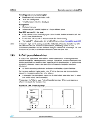

![RM0008 Controller area network (bxCAN)
Figure 222. Dual CAN block diagram (connectivity devices)
CAN1 (Master) with 512 bytes SRAM
Master
Tx Mailboxes Master Master
Receive FIFO 0 Receive FIFO 1
2
1 2 2
Mailbox 0 1 1
Mailbox 0 Mailbox 0
Master Control
Master Status
Tx Status
Rx FIFO 0 Status Transmission
Scheduler
Control/Status/Configuration
Rx FIFO 1 Status
Acceptance Filters
Interrupt Enable
27
CAN 2.0B Active Core .. .. 26
Error Status Memory 2 3
1
Access Filter 0
Bit Timing Controller
Filter Master Master Filters Slave Filters
(0 to n) (n to 27)
Filter Mode
Transmission
Filter Scale Scheduler
Slave Slave
Slave Receive FIFO 0 Receive FIFO 1
Filter FIFO Assign Tx Mailboxes 2 2
Filter Activation 2 1 1
1 Mailbox 0 Mailbox 0
Mailbox 0
CAN2 (Slave)
Control/Status/Configuration
Master Control
Master Status
Tx Status
Rx FIFO 0 Status
CAN 2.0B Active Core
Rx FIFO 1 Status
Interrupt Enable
Error Status
Note: CAN 2 start filter bank number n is configurable by writing to
Bit Timing the CAN2SB[5:0] bits in the CAN_ FMR register.
ai16094
23.4 bxCAN operating modes
bxCAN has three main operating modes: initialization, normal and Sleep. After a
hardware reset, bxCAN is in Sleep mode to reduce power consumption and an internal pull-
up is active on CANTX. The software requests bxCAN to enter initialization or Sleep mode
by setting the INRQ or SLEEP bits in the CAN_MCR register. Once the mode has been
entered, bxCAN confirms it by setting the INAK or SLAK bits in the CAN_MSR register and
the internal pull-up is disabled. When neither INAK nor SLAK are set, bxCAN is in normal
mode. Before entering normal mode bxCAN always has to synchronize on the CAN bus.
Doc ID 13902 Rev 11 613/1072](https://image.slidesharecdn.com/stm32referencemanual-110220082754-phpapp01/85/Stm32-reference-manual-613-320.jpg)


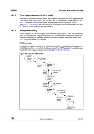
![Controller area network (bxCAN) RM0008
FIFO management
Starting from the empty state, the first valid message received is stored in the FIFO which
becomes pending_1. The hardware signals the event setting the FMP[1:0] bits in the
CAN_RFR register to the value 01b. The message is available in the FIFO output mailbox.
The software reads out the mailbox content and releases it by setting the RFOM bit in the
CAN_RFR register. The FIFO becomes empty again. If a new valid message has been
received in the meantime, the FIFO stays in pending_1 state and the new message is
available in the output mailbox.
If the application does not release the mailbox, the next valid message will be stored in the
FIFO which enters pending_2 state (FMP[1:0] = 10b). The storage process is repeated for
the next valid message putting the FIFO into pending_3 state (FMP[1:0] = 11b). At this
point, the software must release the output mailbox by setting the RFOM bit, so that a
mailbox is free to store the next valid message. Otherwise the next valid message received
will cause a loss of message.
Refer also to Section 23.7.5: Message storage
Overrun
Once the FIFO is in pending_3 state (i.e. the three mailboxes are full) the next valid
message reception will lead to an overrun and a message will be lost. The hardware
signals the overrun condition by setting the FOVR bit in the CAN_RFR register. Which
message is lost depends on the configuration of the FIFO:
● If the FIFO lock function is disabled (RFLM bit in the CAN_MCR register cleared) the
last message stored in the FIFO will be overwritten by the new incoming message. In
this case the latest messages will be always available to the application.
● If the FIFO lock function is enabled (RFLM bit in the CAN_MCR register set) the most
recent message will be discarded and the software will have the three oldest messages
in the FIFO available.
Reception related interrupts
Once a message has been stored in the FIFO, the FMP[1:0] bits are updated and an
interrupt request is generated if the FMPIE bit in the CAN_IER register is set.
When the FIFO becomes full (i.e. a third message is stored) the FULL bit in the CAN_RFR
register is set and an interrupt is generated if the FFIE bit in the CAN_IER register is set.
On overrun condition, the FOVR bit is set and an interrupt is generated if the FOVIE bit in
the CAN_IER register is set.
23.7.4 Identifier filtering
In the CAN protocol the identifier of a message is not associated with the address of a node
but related to the content of the message. Consequently a transmitter broadcasts its
message to all receivers. On message reception a receiver node decides - depending on
the identifier value - whether the software needs the message or not. If the message is
needed, it is copied into the SRAM. If not, the message must be discarded without
intervention by the software.
To fulfill this requirement, in connectivity line devices the bxCAN Controller provides 28
configurable and scalable filter banks (27-0) to the application. In other devices the bxCAN
Controller provides 14 configurable and scalable filter banks (13-0) to the application in
order to receive only the messages the software needs. This hardware filtering saves CPU
620/1072 Doc ID 13902 Rev 11](https://image.slidesharecdn.com/stm32referencemanual-110220082754-phpapp01/85/Stm32-reference-manual-620-320.jpg)
![RM0008 Controller area network (bxCAN)
resources which would be otherwise needed to perform filtering by software. Each filter
bank x consists of two 32-bit registers, CAN_FxR0 and CAN_FxR1.
Scalable width
To optimize and adapt the filters to the application needs, each filter bank can be scaled
independently. Depending on the filter scale a filter bank provides:
● One 32-bit filter for the STDID[10:0], EXTID[17:0], IDE and RTR bits.
● Two 16-bit filters for the STDID[10:0], RTR, IDE and EXTID[17:15] bits.
Refer to Figure 229.
Furthermore, the filters can be configured in mask mode or in identifier list mode.
Mask mode
In mask mode the identifier registers are associated with mask registers specifying which
bits of the identifier are handled as “must match” or as “don’t care”.
Identifier list mode
In identifier list mode, the mask registers are used as identifier registers. Thus instead of
defining an identifier and a mask, two identifiers are specified, doubling the number of single
identifiers. All bits of the incoming identifier must match the bits specified in the filter
registers.
Filter bank scale and mode configuration
The filter banks are configured by means of the corresponding CAN_FMR register. To
configure a filter bank it must be deactivated by clearing the FACT bit in the CAN_FAR
register. The filter scale is configured by means of the corresponding FSCx bit in the
CAN_FS1R register, refer to Figure 229. The identifier list or identifier mask mode for the
corresponding Mask/Identifier registers is configured by means of the FBMx bits in the
CAN_FMR register.
To filter a group of identifiers, configure the Mask/Identifier registers in mask mode.
To select single identifiers, configure the Mask/Identifier registers in identifier list mode.
Filters not used by the application should be left deactivated.
Each filter within a filter bank is numbered (called the Filter Number) from 0 to a maximum
dependent on the mode and the scale of each of the filter banks.
Concerning the filter configuration, refer to Figure 229.
Doc ID 13902 Rev 11 621/1072](https://image.slidesharecdn.com/stm32referencemanual-110220082754-phpapp01/85/Stm32-reference-manual-621-320.jpg)
![Controller area network (bxCAN) RM0008
Figure 229. Filter bank scale configuration - register organization
Filter
One 32-Bit Filter - Identifier Mask Num.
FBMx = 0
ID CAN_FxR1[31:24] CAN_FxR1[23:16] CAN_FxR1[15:8] CAN_FxR1[7:0]
n
Mask CAN_FxR2[31:24] CAN_FxR2[23:16] CAN_FxR2[15:8] CAN_FxR2[7:0]
FSCx = 1
Mapping STID[10:3] STID[2:0] EXID[17:13] EXID[12:5] EXID[4:0] IDE RTR 0
Two 32-Bit Filters - Identifier List
FBMx = 1
ID CAN_FxR1[31:24] CAN_FxR1[23:16] CAN_FxR1[15:8] CAN_FxR1[7:0] n
ID CAN_FxR2[31:24] CAN_FxR2[23:16] CAN_FxR2[15:8] CAN_FxR2[7:0] n+1
Mapping STID[10:3] STID[2:0] EXID[17:13] EXID[12:5] EXID[4:0] IDE RTR 0
Two 16-Bit Filters - Identifier Mask
ID CAN_FxR1[15:8] CAN_FxR1[7:0]
FBMx = 0
n
Mask CAN_FxR1[31:24] CAN_FxR1[23:16]
ID CAN_FxR2[15:8] CAN_FxR2[7:0]
n+1
Mask CAN_FxR2[31:24] CAN_FxR2[23:16]
FSCx = 0
Mapping STID[10:3] STID[2:0] RTR IDE EXID[17:15]
Four 16-Bit Filters - Identifier List
ID CAN_FxR1[15:8] CAN_FxR1[7:0] n
FBMx = 1
ID CAN_FxR1[31:24] CAN_FxR1[23:16] n+1
ID CAN_FxR2[15:8] CAN_FxR2[7:0] n+2
ID CAN_FxR2[31:24] CAN_FxR2[23:16] n+3
Mapping STID[10:3] STID[2:0] RTR IDE EXID[17:15]
Filter Bank Mode2
Filter Bank Scale
Config. Bits1
x = filter bank number
ID=Identifier
1
These bits are located in the CAN_FS1R register
2
These bits are located in the CAN_FM1R register
Filter match index
Once a message has been received in the FIFO it is available to the application. Typically,
application data is copied into SRAM locations. To copy the data to the right location the
application has to identify the data by means of the identifier. To avoid this, and to ease the
access to the SRAM locations, the CAN controller provides a Filter Match Index.
This index is stored in the mailbox together with the message according to the filter priority
rules. Thus each received message has its associated filter match index.
The Filter Match index can be used in two ways:
● Compare the Filter Match index with a list of expected values.
● Use the Filter Match Index as an index on an array to access the data destination
location.
For non-masked filters, the software no longer has to compare the identifier.
If the filter is masked the software reduces the comparison to the masked bits only.
The index value of the filter number does not take into account the activation state of the
filter banks. In addition, two independent numbering schemes are used, one for each FIFO.
Refer to Figure 230 for an example.
622/1072 Doc ID 13902 Rev 11](https://image.slidesharecdn.com/stm32referencemanual-110220082754-phpapp01/85/Stm32-reference-manual-622-320.jpg)

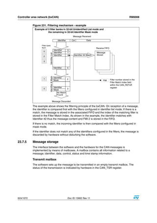
![RM0008 Controller area network (bxCAN)
Table 176. Transmit mailbox mapping
Offset to transmit mailbox base address Register name
0 CAN_TIxR
4 CAN_TDTxR
8 CAN_TDLxR
12 CAN_TDHxR
Receive mailbox
When a message has been received, it is available to the software in the FIFO output
mailbox. Once the software has handled the message (e.g. read it) the software must
release the FIFO output mailbox by means of the RFOM bit in the CAN_RFR register to
make the next incoming message available. The filter match index is stored in the MFMI field
of the CAN_RDTxR register. The 16-bit time stamp value is stored in the TIME[15:0] field of
CAN_RDTxR.
Table 177. Receive mailbox mapping
Offset to receive mailbox base
Register name
address (bytes)
0 CAN_RIxR
4 CAN_RDTxR
8 CAN_RDLxR
12 CAN_RDHxR
Figure 232. CAN error state diagram
Doc ID 13902 Rev 11 625/1072](https://image.slidesharecdn.com/stm32referencemanual-110220082754-phpapp01/85/Stm32-reference-manual-625-320.jpg)

![RM0008 Controller area network (bxCAN)
A valid edge is defined as the first transition in a bit time from dominant to recessive bus
level provided the controller itself does not send a recessive bit.
If a valid edge is detected in BS1 instead of SYNC_SEG, BS1 is extended by up to SJW so
that the sample point is delayed.
Conversely, if a valid edge is detected in BS2 instead of SYNC_SEG, BS2 is shortened by
up to SJW so that the transmit point is moved earlier.
As a safeguard against programming errors, the configuration of the Bit Timing Register
(CAN_BTR) is only possible while the device is in Standby mode.
Note: For a detailed description of the CAN bit timing and resynchronization mechanism, please
refer to the ISO 11898 standard.
Figure 233. Bit timing
NOMINAL BIT TIME
SYNC_SEG BIT SEGMENT 1 (BS1) BIT SEGMENT 2 (BS2)
1 x tq tBS1 tBS2
SAMPLE POINT TRANSMIT POINT
1
BaudRate = ----------------------------------------------
NominalBitTime
NominalBitTime = 1 t q + t BS1 + t BS2
with:
tBS1 = tq x (TS1[3:0] + 1),
tBS2 = tq x (TS2[2:0] + 1),
tq = (BRP[9:0] + 1) x tPCLK
where tq refers to the Time quantum
tPCLK = time period of the APB clock,
BRP[9:0], TS1[3:0] and TS2[2:0] are defined in the CAN_BTR Register.
Doc ID 13902 Rev 11 627/1072](https://image.slidesharecdn.com/stm32referencemanual-110220082754-phpapp01/85/Stm32-reference-manual-627-320.jpg)


![RM0008 Controller area network (bxCAN)
Bit 2 ERRI: Error interrupt
This bit is set by hardware when a bit of the CAN_ESR has been set on error detection and
the corresponding interrupt in the CAN_IER is enabled. Setting this bit generates a status
change interrupt if the ERRIE bit in the CAN_IER register is set.
This bit is cleared by software.
Bit 1 SLAK: Sleep acknowledge
This bit is set by hardware and indicates to the software that the CAN hardware is now in
Sleep mode. This bit acknowledges the Sleep mode request from the software (set SLEEP
bit in CAN_MCR register).
This bit is cleared by hardware when the CAN hardware has left Sleep mode (to be
synchronized on the CAN bus). To be synchronized the hardware has to monitor a
sequence of 11 consecutive recessive bits on the CAN RX signal.
Note: The process of leaving Sleep mode is triggered when the SLEEP bit in the CAN_MCR
register is cleared. Please refer to the AWUM bit of the CAN_MCR register description
for detailed information for clearing SLEEP bit
Bit 0 INAK: Initialization acknowledge
This bit is set by hardware and indicates to the software that the CAN hardware is now in
initialization mode. This bit acknowledges the initialization request from the software (set
INRQ bit in CAN_MCR register).
This bit is cleared by hardware when the CAN hardware has left the initialization mode (to
be synchronized on the CAN bus). To be synchronized the hardware has to monitor a
sequence of 11 consecutive recessive bits on the CAN RX signal.
CAN transmit status register (CAN_TSR)
Address offset: 0x08
Reset value: 0x1C00 0000
31 30 29 28 27 26 25 24 23 22 21 20 19 18 17 16
ABRQ TERR TXOK RQCP
LOW2 LOW1 LOW0 TME2 TME1 TME0 CODE[1:0] ALST2
2 Reserved 2 2 2
r r r r r r r r rs rc_w1 rc_w1 rc_w1 rc_w1
15 14 13 12 11 10 9 8 7 6 5 4 3 2 1 0
ABRQ TERR TXOK RQCP ABRQ TERR TXOK RQCP
Reserved ALST1 ALST0
1 1 1 1 0
Reserved
0 0 0
Res.
rs rc_w1 rc_w1 rc_w1 rc_w1 rs rc_w1 rc_w1 rc_w1 rc_w1
Bit 31 LOW2: Lowest priority flag for mailbox 2
This bit is set by hardware when more than one mailbox are pending for transmission and
mailbox 2 has the lowest priority.
Bit 30 LOW1: Lowest priority flag for mailbox 1
This bit is set by hardware when more than one mailbox are pending for transmission and
mailbox 1 has the lowest priority.
Bit 29 LOW0: Lowest priority flag for mailbox 0
This bit is set by hardware when more than one mailbox are pending for transmission and
mailbox 0 has the lowest priority.
Note: The LOW[2:0] bits are set to zero when only one mailbox is pending.
Bit 28 TME2: Transmit mailbox 2 empty
This bit is set by hardware when no transmit request is pending for mailbox 2.
Doc ID 13902 Rev 11 633/1072](https://image.slidesharecdn.com/stm32referencemanual-110220082754-phpapp01/85/Stm32-reference-manual-633-320.jpg)
![Controller area network (bxCAN) RM0008
Bit 27 TME1: Transmit mailbox 1 empty
This bit is set by hardware when no transmit request is pending for mailbox 1.
Bit 26 TME0: Transmit mailbox 0 empty
This bit is set by hardware when no transmit request is pending for mailbox 0.
Bits 25:24 CODE[1:0]: Mailbox code
In case at least one transmit mailbox is free, the code value is equal to the number of the
next transmit mailbox free.
In case all transmit mailboxes are pending, the code value is equal to the number of the
transmit mailbox with the lowest priority.
Bit 23 ABRQ2: Abort request for mailbox 2
Set by software to abort the transmission request for the corresponding mailbox.
Cleared by hardware when the mailbox becomes empty.
Setting this bit has no effect when the mailbox is not pending for transmission.
Bits 22:20 Reserved, forced by hardware to 0.
Bit 19 TERR2: Transmission error of mailbox 2
This bit is set when the previous TX failed due to an error.
Bit 18 ALST2: Arbitration lost for mailbox 2
This bit is set when the previous TX failed due to an arbitration lost.
Bit 17 TXOK2: Transmission OK of mailbox 2
The hardware updates this bit after each transmission attempt.
0: The previous transmission failed
1: The previous transmission was successful
This bit is set by hardware when the transmission request on mailbox 2 has been completed
successfully. Please refer to Figure 227.
Bit 16 RQCP2: Request completed mailbox2
Set by hardware when the last request (transmit or abort) has been performed.
Cleared by software writing a “1” or by hardware on transmission request (TXRQ2 set in
CAN_TMID2R register).
Clearing this bit clears all the status bits (TXOK2, ALST2 and TERR2) for Mailbox 2.
Bit 15 ABRQ1: Abort request for mailbox 1
Set by software to abort the transmission request for the corresponding mailbox.
Cleared by hardware when the mailbox becomes empty.
Setting this bit has no effect when the mailbox is not pending for transmission.
Bits 14:12 Reserved, forced by hardware to 0.
Bit 11 TERR1: Transmission error of mailbox1
This bit is set when the previous TX failed due to an error.
Bit 10 ALST1: Arbitration lost for mailbox1
This bit is set when the previous TX failed due to an arbitration lost.
Bit 9 TXOK1: Transmission OK of mailbox1
The hardware updates this bit after each transmission attempt.
0: The previous transmission failed
1: The previous transmission was successful
This bit is set by hardware when the transmission request on mailbox 1 has been completed
successfully. Please refer to Figure 227
634/1072 Doc ID 13902 Rev 11](https://image.slidesharecdn.com/stm32referencemanual-110220082754-phpapp01/85/Stm32-reference-manual-634-320.jpg)
![RM0008 Controller area network (bxCAN)
Bit 8 RQCP1: Request completed mailbox1
Set by hardware when the last request (transmit or abort) has been performed.
Cleared by software writing a “1” or by hardware on transmission request (TXRQ1 set in
CAN_TI1R register).
Clearing this bit clears all the status bits (TXOK1, ALST1 and TERR1) for Mailbox 1.
Bit 7 ABRQ0: Abort request for mailbox0
Set by software to abort the transmission request for the corresponding mailbox.
Cleared by hardware when the mailbox becomes empty.
Setting this bit has no effect when the mailbox is not pending for transmission.
Bits 6:4 Reserved, forced by hardware to 0.
Bit 3 TERR0: Transmission error of mailbox0
This bit is set when the previous TX failed due to an error.
Bit 2 ALST0: Arbitration lost for mailbox0
This bit is set when the previous TX failed due to an arbitration lost.
Bit 1 TXOK0: Transmission OK of mailbox0
The hardware updates this bit after each transmission attempt.
0: The previous transmission failed
1: The previous transmission was successful
This bit is set by hardware when the transmission request on mailbox 1 has been completed
successfully. Please refer to Figure 227
Bit 0 RQCP0: Request completed mailbox0
Set by hardware when the last request (transmit or abort) has been performed.
Cleared by software writing a “1” or by hardware on transmission request (TXRQ0 set in
CAN_TI0R register).
Clearing this bit clears all the status bits (TXOK0, ALST0 and TERR0) for Mailbox 0.
CAN receive FIFO 0 register (CAN_RF0R)
Address offset: 0x0C
Reset value: 0x00
31 30 29 28 27 26 25 24 23 22 21 20 19 18 17 16
Reserved
15 14 13 12 11 10 9 8 7 6 5 4 3 2 1 0
RFOM0 FOVR0 FULL0 FMP0[1:0]
Reserved Res.
rs rc_w1 rc_w1 r r
Bit 31:6 Reserved, forced by hardware to 0.
Bit 5 RFOM0: Release FIFO 0 output mailbox
Set by software to release the output mailbox of the FIFO. The output mailbox can only be
released when at least one message is pending in the FIFO. Setting this bit when the FIFO
is empty has no effect. If at least two messages are pending in the FIFO, the software has to
release the output mailbox to access the next message.
Cleared by hardware when the output mailbox has been released.
Doc ID 13902 Rev 11 635/1072](https://image.slidesharecdn.com/stm32referencemanual-110220082754-phpapp01/85/Stm32-reference-manual-635-320.jpg)
![Controller area network (bxCAN) RM0008
Bit 4 FOVR0: FIFO 0 overrun
This bit is set by hardware when a new message has been received and passed the filter
while the FIFO was full.
This bit is cleared by software.
Bit 3 FULL0: FIFO 0 full
Set by hardware when three messages are stored in the FIFO.
This bit is cleared by software.
Bit 2 Reserved, forced by hardware to 0.
Bits 1:0 FMP0[1:0]: FIFO 0 message pending
These bits indicate how many messages are pending in the receive FIFO.
FMP is increased each time the hardware stores a new message in to the FIFO. FMP is
decreased each time the software releases the output mailbox by setting the RFOM0 bit.
CAN receive FIFO 1 register (CAN_RF1R)
Address offset: 0x10
Reset value: 0x00
31 30 29 28 27 26 25 24 23 22 21 20 19 18 17 16
Reserved
15 14 13 12 11 10 9 8 7 6 5 4 3 2 1 0
RFOM1 FOVR1 FULL1 FMP1[1:0]
Reserved Res.
rs rc_w1 rc_w1 r r
Bits 31:6 Reserved, forced by hardware to 0.
Bit 5 RFOM1: Release FIFO 1 output mailbox
Set by software to release the output mailbox of the FIFO. The output mailbox can only be
released when at least one message is pending in the FIFO. Setting this bit when the FIFO
is empty has no effect. If at least two messages are pending in the FIFO, the software has to
release the output mailbox to access the next message.
Cleared by hardware when the output mailbox has been released.
Bit 4 FOVR1: FIFO 1 overrun
This bit is set by hardware when a new message has been received and passed the filter
while the FIFO was full.
This bit is cleared by software.
Bit 3 FULL1: FIFO 1 full
Set by hardware when three messages are stored in the FIFO.
This bit is cleared by software.
Bit 2 Reserved, forced by hardware to 0.
Bits 1:0 FMP1[1:0]: FIFO 1 message pending
These bits indicate how many messages are pending in the receive FIFO1.
FMP1 is increased each time the hardware stores a new message in to the FIFO1. FMP is
decreased each time the software releases the output mailbox by setting the RFOM1 bit.
636/1072 Doc ID 13902 Rev 11](https://image.slidesharecdn.com/stm32referencemanual-110220082754-phpapp01/85/Stm32-reference-manual-636-320.jpg)
![RM0008 Controller area network (bxCAN)
CAN interrupt enable register (CAN_IER)
Address offset: 0x14
Reset value: 0x00
31 30 29 28 27 26 25 24 23 22 21 20 19 18 17 16
SLKIE WKUIE
Reserved
rw rw
15 14 13 12 11 10 9 8 7 6 5 4 3 2 1 0
LEC BOF EPV EWG FOV FF FMP FOV FF FMP TME
ERRIE
Reserved IE IE IE IE Res. IE1 IE1 IE1 IE0 IE0 IE0 IE
rw rw rw rw rw rw rw rw rw rw rw rw
Bits 31:18 Reserved, forced by hardware to 0.
Bit 17 SLKIE: Sleep interrupt enable
0: No interrupt when SLAKI bit is set.
1: Interrupt generated when SLAKI bit is set.
Bit 16 WKUIE: Wakeup interrupt enable
0: No interrupt when WKUI is set.
1: Interrupt generated when WKUI bit is set.
Bit 15 ERRIE: Error interrupt enable
0: No interrupt will be generated when an error condition is pending in the CAN_ESR.
1: An interrupt will be generation when an error condition is pending in the CAN_ESR.
Bits 14:12 Reserved, forced by hardware to 0.
Bit 11 LECIE: Last error code interrupt enable
0: ERRI bit will not be set when the error code in LEC[2:0] is set by hardware on error
detection.
1: ERRI bit will be set when the error code in LEC[2:0] is set by hardware on error detection.
Bit 10 BOFIE: Bus-off interrupt enable
0: ERRI bit will not be set when BOFF is set.
1: ERRI bit will be set when BOFF is set.
Bit 9 EPVIE: Error passive interrupt enable
0: ERRI bit will not be set when EPVF is set.
1: ERRI bit will be set when EPVF is set.
Bit 8 EWGIE: Error warning interrupt enable
0: ERRI bit will not be set when EWGF is set.
1: ERRI bit will be set when EWGF is set.
Bit 7 Reserved, forced by hardware to 0.
Bit 6 FOVIE1: FIFO overrun interrupt enable
0: No interrupt when FOVR is set.
1: Interrupt generation when FOVR is set.
Bit 5 FFIE1: FIFO full interrupt enable
0: No interrupt when FULL bit is set.
1: Interrupt generated when FULL bit is set.
Doc ID 13902 Rev 11 637/1072](https://image.slidesharecdn.com/stm32referencemanual-110220082754-phpapp01/85/Stm32-reference-manual-637-320.jpg)
![Controller area network (bxCAN) RM0008
Bit 4 FMPIE1: FIFO message pending interrupt enable
0: No interrupt generated when state of FMP[1:0] bits are not 00b.
1: Interrupt generated when state of FMP[1:0] bits are not 00b.
Bit 3 FOVIE0: FIFO overrun interrupt enable
0: No interrupt when FOVR bit is set.
1: Interrupt generated when FOVR bit is set.
Bit 2 FFIE0: FIFO full interrupt enable
0: No interrupt when FULL bit is set.
1: Interrupt generated when FULL bit is set.
Bit 1 FMPIE0: FIFO message pending interrupt enable
0: No interrupt generated when state of FMP[1:0] bits are not 00b.
1: Interrupt generated when state of FMP[1:0] bits are not 00b.
Bit 0 TMEIE: Transmit mailbox empty interrupt enable
0: No interrupt when RQCPx bit is set.
1: Interrupt generated when RQCPx bit is set.
Note: Refer to Section 23.8: bxCAN interrupts.
CAN error status register (CAN_ESR)
Address offset: 0x18
Reset value: 0x00
31 30 29 28 27 26 25 24 23 22 21 20 19 18 17 16
REC[7:0] TEC[7:0]
r r r r r r r r r r r r r r r r
15 14 13 12 11 10 9 8 7 6 5 4 3 2 1 0
LEC[2:0] BOFF EPVF EWGF
Reserved Res.
rw rw rw r r r
Bits 31:24 REC[7:0]: Receive error counter
The implementing part of the fault confinement mechanism of the CAN protocol. In case of
an error during reception, this counter is incremented by 1 or by 8 depending on the error
condition as defined by the CAN standard. After every successful reception the counter is
decremented by 1 or reset to 120 if its value was higher than 128. When the counter value
exceeds 127, the CAN controller enters the error passive state.
Bits 23:16 TEC[7:0]: Least significant byte of the 9-bit transmit error counter
The implementing part of the fault confinement mechanism of the CAN protocol.
Bits 15:7 Reserved, forced by hardware to 0.
638/1072 Doc ID 13902 Rev 11](https://image.slidesharecdn.com/stm32referencemanual-110220082754-phpapp01/85/Stm32-reference-manual-638-320.jpg)
![RM0008 Controller area network (bxCAN)
Bits 6:4 LEC[2:0]: Last error code
This field is set by hardware and holds a code which indicates the error condition of the last
error detected on the CAN bus. If a message has been transferred (reception or
transmission) without error, this field will be cleared to ‘0’.
Code 7 is unused and may be written by the hardware to check for an update
000: No Error
001: Stuff Error
010: Form Error
011: Acknowledgment Error
100: Bit recessive Error
101: Bit dominant Error
110: CRC Error
111: Set by software
Bit 3 Reserved, forced by hardware to 0.
Bit 2 BOFF: Bus-off flag
This bit is set by hardware when it enters the bus-off state. The bus-off state is entered on
TEC overflow, greater than 255, refer to Section 23.7.6 on page 626.
Bit 1 EPVF: Error passive flag
This bit is set by hardware when the Error Passive limit has been reached (Receive Error
Counter or Transmit Error Counter>127).
Bit 0 EWGF: Error warning flag
This bit is set by hardware when the warning limit has been reached
(Receive Error Counter or Transmit Error Counter96).
CAN bit timing register (CAN_BTR)
Address offset: 0x1C
Reset value: 0x0123 0000
Note: This register can only be accessed by the software when the CAN hardware is in
initialization mode.
31 30 29 28 27 26 25 24 23 22 21 20 19 18 17 16
SILM LBKM SJW[1:0] Res. TS2[2:0] TS1[3:0]
Reserved
rw rw rw rw rw rw rw rw rw rw rw
15 14 13 12 11 10 9 8 7 6 5 4 3 2 1 0
BRP[9:0]
Reserved
rw rw rw rw rw rw rw rw rw rw
Bit 31 SILM: Silent mode (debug)
0: Normal operation
1: Silent Mode
Bit 30 LBKM: Loop back mode (debug)
0: Loop Back Mode disabled
1: Loop Back Mode enabled
Bits 29:26 Reserved, forced by hardware to 0.
Doc ID 13902 Rev 11 639/1072](https://image.slidesharecdn.com/stm32referencemanual-110220082754-phpapp01/85/Stm32-reference-manual-639-320.jpg)
![Controller area network (bxCAN) RM0008
Bits 25:24 SJW[1:0]: Resynchronization jump width
These bits define the maximum number of time quanta the CAN hardware is allowed to
lengthen or shorten a bit to perform the resynchronization.
tRJW = tCAN x (SJW[1:0] + 1)
Bit 23 Reserved, forced by hardware to 0.
Bits 22:20 TS2[2:0]: Time segment 2
These bits define the number of time quanta in Time Segment 2.
tBS2 = tCAN x (TS2[2:0] + 1)
Bits 19:16 TS1[3:0]: Time segment 1
These bits define the number of time quanta in Time Segment 1
tBS1 = tCAN x (TS1[3:0] + 1)
For more information on bit timing, please refer to Section 23.7.7: Bit timing on page 626.
Bits 15:10 Reserved, forced by hardware to 0.
Bits 9:0 BRP[9:0]: Baud rate prescaler
These bits define the length of a time quanta.
tq = (BRP[9:0]+1) x tPCLK
23.9.3 CAN mailbox registers
This chapter describes the registers of the transmit and receive mailboxes. Refer to
Section 23.7.5: Message storage on page 624 for detailed register mapping.
Transmit and receive mailboxes have the same registers except:
● The FMI field in the CAN_RDTxR register.
● A receive mailbox is always write protected.
● A transmit mailbox is write-enabled only while empty, corresponding TME bit in the
CAN_TSR register set.
There are 3 TX Mailboxes and 2 RX Mailboxes. Each RX Mailbox allows access to a 3 level
depth FIFO, the access being offered only to the oldest received message in the FIFO.
Each mailbox consist of 4 registers.
CAN_RI0R CAN_RI1R CAN_TI0R CAN_TI1R CAN_TI2R
CAN_RDT0R CAN_RDT1R CAN_TDT0R CAN_TDT1R CAN_TDT2R
CAN_RL0R CAN_RL1R CAN_TDL0R CAN_TDL1R CAN_TDL2R
CAN_RH0R CAN_RH1R CAN_TDH0R CAN_TDH1R CAN_TDH2R
FIFO0 FIFO1 Three Tx Mailboxes
640/1072 Doc ID 13902 Rev 11](https://image.slidesharecdn.com/stm32referencemanual-110220082754-phpapp01/85/Stm32-reference-manual-640-320.jpg)
![RM0008 Controller area network (bxCAN)
CAN TX mailbox identifier register (CAN_TIxR) (x=0..2)
Address offsets: 0x180, 0x190, 0x1A0
Reset value: undefined (except bit 0, TXRQ = 0)
Note: 1 All TX registers are write protected when the mailbox is pending transmission (TMEx reset).
2 This register also implements the TX request control (bit 0) - reset value 0.
31 30 29 28 27 26 25 24 23 22 21 20 19 18 17 16
STID[10:0]/EXID[28:18] EXID[17:13]
rw rw rw rw rw rw rw rw rw rw rw rw rw rw rw rw
15 14 13 12 11 10 9 8 7 6 5 4 3 2 1 0
EXID[12:0] IDE RTR TXRQ
rw rw rw rw rw rw rw rw rw rw rw rw rw rw rw rw
Bits 31:21 STID[10:0]/EXID[28:18]: Standard identifier or extended identifier
The standard identifier or the MSBs of the extended identifier (depending on the IDE bit
value).
Bit 20:3 EXID[17:0]: Extended identifier
The LSBs of the extended identifier.
Bit 2 IDE: Identifier extension
This bit defines the identifier type of message in the mailbox.
0: Standard identifier.
1: Extended identifier.
Bit 1 RTR: Remote transmission request
0: Data frame
1: Remote frame
Bit 0 TXRQ: Transmit mailbox request
Set by software to request the transmission for the corresponding mailbox.
Cleared by hardware when the mailbox becomes empty.
Doc ID 13902 Rev 11 641/1072](https://image.slidesharecdn.com/stm32referencemanual-110220082754-phpapp01/85/Stm32-reference-manual-641-320.jpg)
![Controller area network (bxCAN) RM0008
CAN mailbox data length control and time stamp register (CAN_TDTxR)
(x=0..2)
All bits of this register are write protected when the mailbox is not in empty state.
Address offsets: 0x184, 0x194, 0x1A4
Reset value: undefined
31 30 29 28 27 26 25 24 23 22 21 20 19 18 17 16
TIME[15:0]
rw rw rw rw rw rw rw rw rw rw rw rw rw rw rw rw
15 14 13 12 11 10 9 8 7 6 5 4 3 2 1 0
TGT DLC[3:0]
Reserved Reserved
rw rw rw rw rw
Bits 31:16 TIME[15:0]: Message time stamp
This field contains the 16-bit timer value captured at the SOF transmission.
Bits 15:9 Reserved
Bit 8 TGT: Transmit global time
This bit is active only when the hardware is in the Time Trigger Communication mode, TTCM
bit of the CAN_MCR register is set.
0: Time stamp TIME[15:0] is not sent.
1: Time stamp TIME[15:0] value is sent in the last two data bytes of the 8-byte message:
TIME[7:0] in data byte 7 and TIME[15:8] in data byte 6, replacing the data written in
CAN_TDHxR[31:16] register (DATA6[7:0] and DATA7[7:0]). DLC must be programmed as 8
in order these two bytes to be sent over the CAN bus.
Bits 7:4 Reserved
Bits 3:0 DLC[3:0]: Data length code
This field defines the number of data bytes a data frame contains or a remote frame request.
A message can contain from 0 to 8 data bytes, depending on the value in the DLC field.
642/1072 Doc ID 13902 Rev 11](https://image.slidesharecdn.com/stm32referencemanual-110220082754-phpapp01/85/Stm32-reference-manual-642-320.jpg)
![RM0008 Controller area network (bxCAN)
CAN mailbox data low register (CAN_TDLxR) (x=0..2)
All bits of this register are write protected when the mailbox is not in empty state.
Address offsets: 0x188, 0x198, 0x1A8
Reset value: undefined
31 30 29 28 27 26 25 24 23 22 21 20 19 18 17 16
DATA3[7:0] DATA2[7:0]
rw rw rw rw rw rw rw rw rw rw rw rw rw rw rw rw
15 14 13 12 11 10 9 8 7 6 5 4 3 2 1 0
DATA1[7:0] DATA0[7:0]
rw rw rw rw rw rw rw rw rw rw rw rw rw rw rw rw
Bits 31:24 DATA3[7:0]: Data byte 3
Data byte 3 of the message.
Bits 23:16 DATA2[7:0]: Data byte 2
Data byte 2 of the message.
Bits 15:8 DATA1[7:0]: Data byte 1
Data byte 1 of the message.
Bits 7:0 DATA0[7:0]: Data byte 0
Data byte 0 of the message.
A message can contain from 0 to 8 data bytes and starts with byte 0.
CAN mailbox data high register (CAN_TDHxR) (x=0..2)
All bits of this register are write protected when the mailbox is not in empty state.
Address offsets: 0x18C, 0x19C, 0x1AC
Reset value: undefined
31 30 29 28 27 26 25 24 23 22 21 20 19 18 17 16
DATA7[7:0] DATA6[7:0]
rw rw rw rw rw rw rw rw rw rw rw rw rw rw rw rw
15 14 13 12 11 10 9 8 7 6 5 4 3 2 1 0
DATA5[7:0] DATA4[7:0]
rw rw rw rw rw rw rw rw rw rw rw rw rw rw rw rw
Bits 31:24 DATA7[7:0]: Data byte 7
Data byte 7 of the message.
Note: If TGT of this message and TTCM are active, DATA7 and DATA6 will be replaced by the
TIME stamp value.
Bits 23:16 DATA6[7:0]: Data byte 6
Data byte 6 of the message.
Bits 15:8 DATA5[7:0]: Data byte 5
Data byte 5 of the message.
Bits 7:0 DATA4[7:0]: Data byte 4
Data byte 4 of the message.
Doc ID 13902 Rev 11 643/1072](https://image.slidesharecdn.com/stm32referencemanual-110220082754-phpapp01/85/Stm32-reference-manual-643-320.jpg)
![Controller area network (bxCAN) RM0008
CAN receive FIFO mailbox identifier register (CAN_RIxR) (x=0..1)
Address offsets: 0x1B0, 0x1C0
Reset value: undefined
Note: All RX registers are write protected.
31 30 29 28 27 26 25 24 23 22 21 20 19 18 17 16
STID[10:0]/EXID[28:18] EXID[17:13]
r r r r r r r r r r r r r r r r
15 14 13 12 11 10 9 8 7 6 5 4 3 2 1 0
EXID[12:0] IDE RTR
Res.
r r r r r r r r r r r r r r r
Bits 31:21 STID[10:0]/EXID[28:18]: Standard identifier or extended identifier
The standard identifier or the MSBs of the extended identifier (depending on the IDE bit
value).
Bits 20:3 EXID[17:0]: Extended identifier
The LSBs of the extended identifier.
Bit 2 IDE: Identifier extension
This bit defines the identifier type of message in the mailbox.
0: Standard identifier.
1: Extended identifier.
Bit 1 RTR: Remote transmission request
0: Data frame
1: Remote frame
Bit 0 Reserved
644/1072 Doc ID 13902 Rev 11](https://image.slidesharecdn.com/stm32referencemanual-110220082754-phpapp01/85/Stm32-reference-manual-644-320.jpg)
![RM0008 Controller area network (bxCAN)
CAN receive FIFO mailbox data length control and time stamp register
(CAN_RDTxR) (x=0..1)
Address offsets: 0x1B4, 0x1C4
Reset value: undefined
Note: All RX registers are write protected.
31 30 29 28 27 26 25 24 23 22 21 20 19 18 17 16
TIME[15:0]
r r r r r r r r r r r r r r r r
15 14 13 12 11 10 9 8 7 6 5 4 3 2 1 0
FMI[7:0] DLC[3:0]
Reserved
r r r r r r r r r r r r
Bits 31:16 TIME[15:0]: Message time stamp
This field contains the 16-bit timer value captured at the SOF detection.
Bits 15:8 FMI[7:0]: Filter match index
This register contains the index of the filter the message stored in the mailbox passed
through. For more details on identifier filtering please refer to Section 23.7.4: Identifier
filtering on page 620 - Filter Match Index paragraph.
Bits 7:4 Reserved, forced by hardware to 0.
Bits 3:0 DLC[3:0]: Data length code
This field defines the number of data bytes a data frame contains (0 to 8). It is 0 in the case
of a remote frame request.
Doc ID 13902 Rev 11 645/1072](https://image.slidesharecdn.com/stm32referencemanual-110220082754-phpapp01/85/Stm32-reference-manual-645-320.jpg)
![Controller area network (bxCAN) RM0008
CAN receive FIFO mailbox data low register (CAN_RDLxR) (x=0..1)
All bits of this register are write protected when the mailbox is not in empty state.
Address offsets: 0x1B8, 0x1C8
Reset value: undefined
Note: All RX registers are write protected.
31 30 29 28 27 26 25 24 23 22 21 20 19 18 17 16
DATA3[7:0] DATA2[7:0]
r r r r r r r r r r r r r r r r
15 14 13 12 11 10 9 8 7 6 5 4 3 2 1 0
DATA1[7:0] DATA0[7:0]
r r r r r r r r r r r r r r r r
Bits 31:24 DATA3[7:0]: Data Byte 3
Data byte 3 of the message.
Bits 23:16 DATA2[7:0]: Data Byte 2
Data byte 2 of the message.
Bits 15:8 DATA1[7:0]: Data Byte 1
Data byte 1 of the message.
Bits 7:0 DATA0[7:0]: Data Byte 0
Data byte 0 of the message.
A message can contain from 0 to 8 data bytes and starts with byte 0.
CAN receive FIFO mailbox data high register (CAN_RDHxR) (x=0..1)
Address offsets: 0x1BC, 0x1CC
Reset value: undefined
Note: All RX registers are write protected.
31 30 29 28 27 26 25 24 23 22 21 20 19 18 17 16
DATA7[7:0] DATA6[7:0]
r r r r r r r r r r r r r r r r
15 14 13 12 11 10 9 8 7 6 5 4 3 2 1 0
DATA5[7:0] DATA4[7:0]
r r r r r r r r r r r r r r r r
Bits 31:24 DATA7[7:0]: Data Byte 7
Data byte 3 of the message.
Bits 23:16 DATA6[7:0]: Data Byte 6
Data byte 2 of the message.
646/1072 Doc ID 13902 Rev 11](https://image.slidesharecdn.com/stm32referencemanual-110220082754-phpapp01/85/Stm32-reference-manual-646-320.jpg)
![RM0008 Controller area network (bxCAN)
Bits 15:8 DATA5[7:0]: Data Byte 5
Data byte 1 of the message.
Bits 7:0 DATA4[7:0]: Data Byte 4
Data byte 0 of the message.
23.9.4 CAN filter registers
CAN filter master register (CAN_FMR)
Address offset: 0x200
Reset value: 0x2A1C 0E01
Note: All bits of this register are set and cleared by software.
31 30 29 28 27 26 25 24 23 22 21 20 19 18 17 16
Reserved
15 14 13 12 11 10 9 8 7 6 5 4 3 2 1 0
FINIT
Reserved
rw
CAN2SB[5:0] FINIT
Reserved Reserved
rw rw rw rw rw rw rw
Bits 31:14 Reserved, forced to reset value
Bits 13:8 CAN2SB[5:0]: CAN2 start bank
These bits are set and cleared by software. They define the start bank for the CAN2
interface (Slave) in the range 1 to 27.
Note: These bits are available in connectivity line devices only and are reserved otherwise.
Bits 7:1 Reserved, forced to reset value
Bit 0 FINIT: Filter init mode
Initialization mode for filter banks
0: Active filters mode.
1: Initialization mode for the filters.
Doc ID 13902 Rev 11 647/1072](https://image.slidesharecdn.com/stm32referencemanual-110220082754-phpapp01/85/Stm32-reference-manual-647-320.jpg)

![RM0008 Controller area network (bxCAN)
CAN filter FIFO assignment register (CAN_FFA1R)
Address offset: 0x214
Reset value: 0x00
Note: This register can be written only when the filter initialization mode is set (FINIT=1) in the
CAN_FMR register.
31 30 29 28 27 26 25 24 23 22 21 20 19 18 17 16
FFA27 FFA26 FFA25 FFA24 FFA23 FFA22 FFA21 FFA20 FFA19 FFA18 FFA17 FFA16
Reserved
rw rw rw rw rw rw rw rw rw rw rw rw
15 14 13 12 11 10 9 8 7 6 5 4 3 2 1 0
FFA15 FFA14 FFA13 FFA12 FFA11 FFA10 FFA9 FFA8 FFA7 FFA6 FFA5 FFA4 FFA3 FFA2 FFA1 FFA0
rw rw rw rw rw rw rw rw rw rw rw rw rw rw rw rw
Bits 31:28 Reserved, forced by hardware to 0.
Bits 27:0 FFAx: Filter FIFO assignment for filter x
The message passing through this filter will be stored in the specified FIFO.
0: Filter assigned to FIFO 0
1: Filter assigned to FIFO 1
Note: Bits 27:14 are available in connectivity line devices only and are reserved otherwise.
CAN filter activation register (CAN_FA1R)
Address offset: 0x21C
Reset value: 0x00
31 30 29 28 27 26 25 24 23 22 21 20 19 18 17 16
FACT27 FACT26 FACT25 FACT24 FACT23 FACT22 FACT21 FACT20 FACT19 FACT18 FACT17 FACT16
Reserved
rw rw rw rw rw rw rw rw rw rw rw rw
15 14 13 12 11 10 9 8 7 6 5 4 3 2 1 0
FACT15 FACT14 FACT13 FACT12 FACT11 FACT10 FACT9 FACT8 FACT7 FACT6 FACT5 FACT4 FACT3 FACT2 FACT1 FACT0
rw rw rw rw rw rw rw rw rw rw rw rw rw rw rw rw
Bits 31:28 Reserved, forced by hardware to 0.
Bits 27:0 FACTx: Filter active
The software sets this bit to activate Filter x. To modify the Filter x registers (CAN_FxR[0:7]),
the FACTx bit must be cleared or the FINIT bit of the CAN_FMR register must be set.
0: Filter x is not active
1: Filter x is active
Note: Bits 27:14 are available in connectivity line devices only and are reserved otherwise.
Doc ID 13902 Rev 11 649/1072](https://image.slidesharecdn.com/stm32referencemanual-110220082754-phpapp01/85/Stm32-reference-manual-649-320.jpg)
![Controller area network (bxCAN) RM0008
Filter bank i register x (CAN_FiRx) (i=0..27 in connectivity line devices,, x=1,
2)
Address offsets: 0x240..0x31C
Reset value: undefined
Note: In connectivity line devices there are 28 filter banks, i=0 .. 27, in other devices there are 14
filter banks i = 0 ..13. Each filter bank i is composed of two 32-bit registers, CAN_FiR[2:1].
This register can only be modified when the FACTx bit of the CAN_FAxR register is cleared
or when the FINIT bit of the CAN_FMR register is set.
31 30 29 28 27 26 25 24 23 22 21 20 19 18 17 16
FB31 FB30 FB29 FB28 FB27 FB26 FB25 FB24 FB23 FB22 FB21 FB20 FB19 FB18 FB17 FB16
rw rw rw rw rw rw rw rw rw rw rw rw rw rw rw rw
15 14 13 12 11 10 9 8 7 6 5 4 3 2 1 0
FB15 FB14 FB13 FB12 FB11 FB10 FB9 FB8 FB7 FB6 FB5 FB4 FB3 FB2 FB1 FB0
rw rw rw rw rw rw rw rw rw rw rw rw rw rw rw rw
In all configurations:
Bits 31:0 FB[31:0]: Filter bits
Identifier
Each bit of the register specifies the level of the corresponding bit of the expected identifier.
0: Dominant bit is expected
1: Recessive bit is expected
Mask
Each bit of the register specifies whether the bit of the associated identifier register must
match with the corresponding bit of the expected identifier or not.
0: Don’t care, the bit is not used for the comparison
1: Must match, the bit of the incoming identifier must have the same level has specified in
the corresponding identifier register of the filter.
Note: Depending on the scale and mode configuration of the filter the function of each register can
differ. For the filter mapping, functions description and mask registers association, refer to
Section 23.7.4: Identifier filtering on page 620.
A Mask/Identifier register in mask mode has the same bit mapping as in identifier list
mode.
For the register mapping/addresses of the filter banks please refer to the Table 178 on
page 651.
650/1072 Doc ID 13902 Rev 11](https://image.slidesharecdn.com/stm32referencemanual-110220082754-phpapp01/85/Stm32-reference-manual-650-320.jpg)
![RM0008 Controller area network (bxCAN)
23.9.5 bxCAN register map
Refer to Table 1 on page 44 for the register boundary addresses. In connectivity line
devices, the registers from offset 0x200 to 31C are present only in CAN1.
Table 178. bxCAN register map and reset values
31
30
29
28
27
26
25
24
23
22
21
20
19
18
17
16
15
14
13
12
11
10
Offset Register
9
8
7
6
5
4
3
2
1
0
RESET
SLEEP
AWUM
ABOM
TTCM
RFLM
NART
TXFP
INRQ
DBF
CAN_MCR
0x000 Reserved Reserved
Reset value 1 0 0 0 0 0 0 0 1 0
SAMP
SLAKI
WKUI
SLAK
ERRI
INAK
RXM
TXM
RX
CAN_MSR
0x004 Reserved Reserved
Reset value 1 1 0 0 0 0 0 1 0
CODE[1:0]
RQCP2
RQCP1
RQCP0
ABRQ2
ABRQ1
ABRQ0
TERR2
TXOK2
TERR1
TXOK1
TERR0
TXOK0
ALST2
ALST1
ALST0
CAN_TSR LOW[2:0] TME[2:0]
0x008 Reserved Reserved Reserved
Reset value 0 0 0 1 1 1 0 0 0 0 0 0 0 0 0 0 0 0 0 0 0 0 0
FMP0[1:0]
RFOM0
FOVR0
FULL0
Reserved
CAN_RF0R
0x00C Reserved
Reset value 0 0 0 0 0
FMP1[1:0]
RFOM1
FOVR1
FULL1
Reserved
CAN_RF1R
0x010 Reserved
Reset value 0 0 0 0 0
FMPIE1
FMPIE0
FOVIE1
FOVIE0
EWGIE
WKUIE
ERRIE
TMEIE
Reserved
BOFIE
EPVIE
LECIE
SLKIE
FFIE1
FFIE0
CAN_IER
0x014 Reserved Reserved
Reset value 0 0 0 0 0 0 0 0 0 0 0 0 0 0
LEC[2:0]
EWGF
Reserved
BOFF
EPVF
CAN_ESR REC[7:0] TEC[7:0]
0x018 Reserved
Reset value 0 0 0 0 0 0 0 0 0 0 0 0 0 0 0 0 0 0 0 0 0 0
SJW[1:0]
Reserved
LBKM
SILM
CAN_BTR TS2[2:0] TS1[3:0] BRP[9:0]
0x01C Reserved Reserved
Reset value 0 0 0 0 0 1 0 0 0 1 1 0 0 0 0 0 0 0 0 0 0
0x020-
Reserved
0x17F TXRQ
RTR
IDE
CAN_TI0R STID[10:0]/EXID[28:18] EXID[17:0]
0x180
Reset value x x x x x x x x x x x x x x x x x x x x x x x x x x x x x x x 0
TGT
CAN_TDT0R TIME[15:0] DLC[3:0]
0x184 Reserved Reserved
Reset value x x x x x x x x x x x x x x x x x x x x x
CAN_TDL0R DATA3[7:0] DATA2[7:0] DATA1[7:0] DATA0[7:0]
0x188
Reset value x x x x x x x x x x x x x x x x x x x x x x x x x x x x x x x x
CAN_TDH0R DATA7[7:0] DATA6[7:0] DATA5[7:0] DATA4[7:0]
0x18C
Reset value x x x x x x x x x x x x x x x x x x x x x x x x x x x x x x x x
TXRQ
RTR
IDE
CAN_TI1R STID[10:0]/EXID[28:18] EXID[17:0]
0x190
Reset value x x x x x x x x x x x x x x x x x x x x x x x x x x x x x x x 0
Doc ID 13902 Rev 11 651/1072](https://image.slidesharecdn.com/stm32referencemanual-110220082754-phpapp01/85/Stm32-reference-manual-651-320.jpg)
![Controller area network (bxCAN) RM0008
Table 178. bxCAN register map and reset values (continued)
31
30
29
28
27
26
25
24
23
22
21
20
19
18
17
16
15
14
13
12
11
10
Offset Register
9
8
7
6
5
4
3
2
1
0
TGT
CAN_TDT1R TIME[15:0] DLC[3:0]
0x194 Reserved Reserved
Reset value x x x x x x x x x x x x x x x x x x x x x
CAN_TDL1R DATA3[7:0] DATA2[7:0] DATA1[7:0] DATA0[7:0]
0x198
Reset value x x x x x x x x x x x x x x x x x x x x x x x x x x x x x x x x
CAN_TDH1R DATA7[7:0] DATA6[7:0] DATA5[7:0] DATA4[7:0]
0x19C
Reset value x x x x x x x x x x x x x x x x x x x x x x x x x x x x x x x x
TXRQ
RTR
IDE
CAN_TI2R STID[10:0]/EXID[28:18] EXID[17:0]
0x1A0
Reset value x x x x x x x x x x x x x x x x x x x x x x x x x x x x x x x 0
TGT
CAN_TDT2R TIME[15:0] DLC[3:0]
0x1A4 Reserved Reserved
Reset value x x x x x x x x x x x x x x x x x x x x x
CAN_TDL2R DATA3[7:0] DATA2[7:0] DATA1[7:0] DATA0[7:0]
0x1A8
Reset value x x x x x x x x x x x x x x x x x x x x x x x x x x x x x x x x
CAN_TDH2R DATA7[7:0] DATA6[7:0] DATA5[7:0] DATA4[7:0]
0x1AC
Reset value x x x x x x x x x x x x x x x x x x x x x x x x x x x x x x x x
Reserved
RTR
IDE
CAN_RI0R STID[10:0]/EXID[28:18] EXID[17:0]
0x1B0
Reset value x x x x x x x x x x x x x x x x x x x x x x x x x x x x x x x
CAN_RDT0R TIME[15:0] FMI[7:0] DLC[3:0]
0x1B4 Reserved
Reset value x x x x x x x x x x x x x x x x x x x x x x x x x x x x
CAN_RDL0R DATA3[7:0] DATA2[7:0] DATA1[7:0] DATA0[7:0]
0x1B8
Reset value x x x x x x x x x x x x x x x x x x x x x x x x x x x x x x x x
CAN_RDH0R DATA7[7:0] DATA6[7:0] DATA5[7:0] DATA4[7:0]
0x1BC
Reset value x x x x x x x x x x x x x x x x x x x x x x x x x x x x x x x x
Reserved
RTR
IDE
CAN_RI1R STID[10:0]/EXID[28:18] EXID[17:0]
0x1C0
Reset value x x x x x x x x x x x x x x x x x x x x x x x x x x x x x x x
CAN_RDT1R TIME[15:0] FMI[7:0] DLC[3:0]
0x1C4 Reserved
Reset value x x x x x x x x x x x x x x x x x x x x x x x x x x x x
CAN_RDL1R DATA3[7:0] DATA2[7:0] DATA1[7:0] DATA0[7:0]
0x1C8
Reset value x x x x x x x x x x x x x x x x x x x x x x x x x x x x x x x x
CAN_RDH1R DATA7[7:0] DATA6[7:0] DATA5[7:0] DATA4[7:0]
0x1CC
Reset value x x x x x x x x x x x x x x x x x x x x x x x x x x x x x x x x
0x1D0-
Reserved
0x1FF
652/1072 Doc ID 13902 Rev 11](https://image.slidesharecdn.com/stm32referencemanual-110220082754-phpapp01/85/Stm32-reference-manual-652-320.jpg)
![RM0008 Controller area network (bxCAN)
Table 178. bxCAN register map and reset values (continued)
31
30
29
28
27
26
25
24
23
22
21
20
19
18
17
16
15
14
13
12
11
10
Offset Register
9
8
7
6
5
4
3
2
1
0 FINIT
CAN_FMR CAN2SB[5:0]
0x200 Reserved Reserved
Reset value 0 0 1 1 1 0 1
CAN_FM1R FBM[27:0]
0x204 Reserved
Reset value 0 0 0 0 0 0 0 0 0 0 0 0 0 0 0 0 0 0 0 0 0 0 0 0 0 0 0 0
0x208 Reserved
CAN_FS1R FSC[27:0]
0x20C Reserved
Reset value 0 0 0 0 0 0 0 0 0 0 0 0 0 0 0 0 0 0 0 0 0 0 0 0 0 0 0 0
0x210 Reserved
CAN_FFA1R FFA[27:0]
0x214 Reserved
Reset value 0 0 0 0 0 0 0 0 0 0 0 0 0 0 0 0 0 0 0 0 0 0 0 0 0 0 0 0
0x218 Reserved
CAN_FA1R FACT[27:0]
0x21C Reserved
Reset value 0 0 0 0 0 0 0 0 0 0 0 0 0 0 0 0 0 0 0 0 0 0 0 0 0 0 0 0
0x220 Reserved
0x224-
Reserved
0x23F
CAN_F0R1 FB[31:0]
0x240
Reset value x x x x x x x x x x x x x x x x x x x x x x x x x x x x x x x x
CAN_F0R2 FB[31:0]
0x244
Reset value x x x x x x x x x x x x x x x x x x x x x x x x x x x x x x x x
CAN_F1R1 FB[31:0]
0x248
Reset value x x x x x x x x x x x x x x x x x x x x x x x x x x x x x x x x
CAN_F1R2 FB[31:0]
0x24C
Reset value x x x x x x x x x x x x x x x x x x x x x x x x x x x x x x x x
. . .
. . .
. . .
. . .
CAN_F27R1 FB[31:0]
0x318
Reset value x x x x x x x x x x x x x x x x x x x x x x x x x x x x x x x x
CAN_F27R2 FB[31:0]
0x31C
Reset value x x x x x x x x x x x x x x x x x x x x x x x x x x x x x x x x
Doc ID 13902 Rev 11 653/1072](https://image.slidesharecdn.com/stm32referencemanual-110220082754-phpapp01/85/Stm32-reference-manual-653-320.jpg)


![RM0008 Serial peripheral interface (SPI)
24.3 SPI functional description
24.3.1 General description
The block diagram of the SPI is shown in Figure 236.
Figure 236. SPI block diagram
Address and data bus
Read
Rx buffer
MOSI SPI_CR2
TXE RXNE ERR TXDM RXDM
0 0 SSOE AEN AEN
IE IE IE
Shift register
MISO
LSB first SPI_SR
MOD CRC
BSY OVR ERR 0 0 TXE RXNE
Tx buffer F
Write
0
Communication
control 1
SCK BR[2:0]
Baud rate generator
LSB SPE BR2 BR1 BR0 MSTR CPOL CPHA
FIRST
SPI_CR1
Master control logic BIDI BIDI CRC CRC RX
MODE OE EN Next DFF ONLY SSM SSI
NSS
ai14744
Usually, the SPI is connected to external devices through 4 pins:
● MISO: Master In / Slave Out data. This pin can be used to transmit data in slave mode
and receive data in master mode.
● MOSI: Master Out / Slave In data. This pin can be used to transmit data in master
mode and receive data in slave mode.
● SCK: Serial Clock output for SPI masters and input for SPI slaves.
● NSS: Slave select. This is an optional pin to select a slave device. This pin acts as a
‘chip select’ to let the SPI master communicate with slaves individually and to avoid
contention on the data lines. Slave NSS inputs can be driven by standard IO ports on
the master device. The NSS pin may also be used as an output if enabled (SSOE bit)
and driven low if the SPI is in master configuration. In this manner, all NSS pins from
devices connected to the Master NSS pin see a low level and become slaves when
they are configured in NSS hardware mode. When configured in master mode with
NSS configured as an input (MSTR=1 and SSOE=0) and if NSS is pulled low, the SPI
enters the master mode fault state: the MSTR bit is automatically cleared and the
device is configured in slave mode (refer to Section 24.3.10: Error flags on page 674).
Doc ID 13902 Rev 11 657/1072](https://image.slidesharecdn.com/stm32referencemanual-110220082754-phpapp01/85/Stm32-reference-manual-657-320.jpg)


![Serial peripheral interface (SPI) RM0008
Figure 239. Data clock timing diagram
1. These timings are shown with the LSBFIRST bit reset in the SPI_CR1 register.
Data frame format
Data can be shifted out either MSB-first or LSB-first depending on the value of the
LSBFIRST bit in the SPI_CR1 Register.
Each data frame is 8 or 16 bits long depending on the size of the data programmed using
the DFF bit in the SPI_CR1 register. The selected data frame format is applicable for
transmission and/or reception.
24.3.2 Configuring the SPI in slave mode
In the slave configuration, the serial clock is received on the SCK pin from the master
device. The value set in the BR[2:0] bits in the SPI_CR1 register, does not affect the data
transfer rate.
Note: It is recommended to enable the SPI slave before the master sends the clock. If not,
undesired data transmission might occur. The data register of the slave needs to be ready
before the first edge of the communication clock or before the end of the ongoing
communication. It is mandatory to have the polarity of the communication clock set to the
steady state value before the slave and the master are enabled.
Follow the procedure below to configure the SPI in slave mode:
660/1072 Doc ID 13902 Rev 11](https://image.slidesharecdn.com/stm32referencemanual-110220082754-phpapp01/85/Stm32-reference-manual-660-320.jpg)
![RM0008 Serial peripheral interface (SPI)
Procedure
1. Set the DFF bit to define 8- or 16-bit data frame format
2. Select the CPOL and CPHA bits to define one of the four relationships between the
data transfer and the serial clock (see Figure 239). For correct data transfer, the CPOL
and CPHA bits must be configured in the same way in the slave device and the master
device.
3. The frame format (MSB-first or LSB-first depending on the value of the LSBFIRST bit in
the SPI_CR1 register) must be the same as the master device.
4. In Hardware mode (refer to Slave select (NSS) pin management on page 658), the
NSS pin must be connected to a low level signal during the complete byte transmit
sequence. In NSS software mode, set the SSM bit and clear the SSI bit in the SPI_CR1
register.
5. Clear the MSTR bit and set the SPE bit (both in the SPI_CR1 register) to assign the
pins to alternate functions.
In this configuration the MOSI pin is a data input and the MISO pin is a data output.
Transmit sequence
The data byte is parallel-loaded into the Tx buffer during a write cycle.
The transmit sequence begins when the slave device receives the clock signal and the most
significant bit of the data on its MOSI pin. The remaining bits (the 7 bits in 8-bit data frame
format, and the 15 bits in 16-bit data frame format) are loaded into the shift-register. The
TXE flag in the SPI_SR register is set on the transfer of data from the Tx Buffer to the shift
register and an interrupt is generated if the TXEIE bit in the SPI_CR2 register is set.
Receive sequence
For the receiver, when data transfer is complete:
● The Data in shift register is transferred to Rx Buffer and the RXNE flag (SPI_SR
register) is set
● An Interrupt is generated if the RXNEIE bit is set in the SPI_CR2 register.
After the last sampling clock edge the RXNE bit is set, a copy of the data byte received in
the shift register is moved to the Rx buffer. When the SPI_DR register is read, the SPI
peripheral returns this buffered value.
Clearing of the RXNE bit is performed by reading the SPI_DR register.
24.3.3 Configuring the SPI in master mode
In the master configuration, the serial clock is generated on the SCK pin.
Procedure
1. Select the BR[2:0] bits to define the serial clock baud rate (see SPI_CR1 register).
2. Select the CPOL and CPHA bits to define one of the four relationships between the
data transfer and the serial clock (see Figure 239).
3. Set the DFF bit to define 8- or 16-bit data frame format
4. Configure the LSBFIRST bit in the SPI_CR1 register to define the frame format
5. If the NSS pin is required in input mode, in hardware mode, connect the NSS pin to a
high-level signal during the complete byte transmit sequence. In NSS software mode,
Doc ID 13902 Rev 11 661/1072](https://image.slidesharecdn.com/stm32referencemanual-110220082754-phpapp01/85/Stm32-reference-manual-661-320.jpg)


![Serial peripheral interface (SPI) RM0008
Figure 248. I2S block diagram
Address and data bus
Tx buffer
BSY OVR MODF CRC UDR CH TxE RxNE
ERR SIDE
16-bit
MOSI/ SD
Shift register
MISO
LSB first Communication
16-bit control
Rx buffer
NSS/WS
I2SCFG I2SSTD CKPOL DATLEN CH
[1:0] [1:0] [1:0] LEN
I2S I2SE
MOD
Master control logic
Bidi Bidi CRCCRC Rx
mode OE EN Next DFF only SSM SSI
SPI LSB
SPE BR2 BR1 BR0 MSTR CPOL CPHA
baud rate generator First
CK
I2S clock generator
I2S_CK
I2SMOD
MCK
MCKOE ODD I2SDIV[7:0]
I2SxCLK
ai14748
The SPI could function as an audio I2S interface when the I2S capability is enabled (by
setting the I2SMOD bit in the SPI_I2SCFGR register). This interface uses almost the same
pins, flags and interrupts as the SPI.
The I2S shares three common pins with the SPI:
● SD: Serial Data (mapped on the MOSI pin) to transmit or receive the two time-
multiplexed data channels (in simplex mode only).
● WS: Word Select (mapped on the NSS pin) is the data control signal output in master
mode and input in slave mode.
● CK: Serial Clock (mapped on the SCK pin) is the serial clock output in master mode
and serial clock input in slave mode.
676/1072 Doc ID 13902 Rev 11](https://image.slidesharecdn.com/stm32referencemanual-110220082754-phpapp01/85/Stm32-reference-manual-676-320.jpg)
![RM0008 Serial peripheral interface (SPI)
An additional pin could be used when a master clock output is needed for some external
audio devices:
● MCK: Master Clock (mapped separately) is used, when the I2S is configured in master
mode (and when the MCKOE bit in the SPI_I2SPR register is set), to output this
additional clock generated at a preconfigured frequency rate equal to 256 × FS, where
FS is the audio sampling frequency.
The I2S uses its own clock generator to produce the communication clock when it is set in
master mode. This clock generator is also the source of the master clock output. Two
additional registers are available in I2S mode. One is linked to the clock generator
configuration SPI_I2SPR and the other one is a generic I2S configuration register
SPI_I2SCFGR (audio standard, slave/master mode, data format, packet frame, clock
polarity, etc.).
The SPI_CR1 register and all CRC registers are not used in the I2S mode. Likewise, the
SSOE bit in the SPI_CR2 register and the MODF and CRCERR bits in the SPI_SR are not
used.
The I2S uses the same SPI register for data transfer (SPI_DR) in 16-bit wide mode.
24.4.2 Supported audio protocols
The three-line bus has to handle only audio data generally time-multiplexed on two
channels: the right channel and the left channel. However there is only one 16-bit register for
the transmission or the reception. So, it is up to the software to write into the data register
the adequate value corresponding to the considered channel side, or to read the data from
the data register and to identify the corresponding channel by checking the CHSIDE bit in
the SPI_SR register. Channel Left is always sent first followed by the channel right (CHSIDE
has no meaning for the PCM protocol).
Four data and packet frames are available. Data may be sent with a format of:
● 16-bit data packed in 16-bit frame
● 16-bit data packed in 32-bit frame
● 24-bit data packed in 32-bit frame
● 32-bit data packed in 32-bit frame
When using 16-bit data extended on 32-bit packet, the first 16 bits (MSB) are the significant
bits, the 16-bit LSB is forced to 0 without any need for software action or DMA request (only
one read/write operation).
The 24-bit and 32-bit data frames need two CPU read or write operations to/from the
SPI_DR or two DMA operations if the DMA is preferred for the application. For 24-bit data
frame specifically, the 8 non-significant bits are extended to 32 bits with 0-bits (by hardware).
For all data formats and communication standards, the most significant bit is always sent
first (MSB first).
The I2S interface supports four audio standards, configurable using the I2SSTD[1:0] and
PCMSYNC bits in the SPI_I2SCFGR register.
I2S Phillips standard
For this standard, the WS signal is used to indicate which channel is being transmitted. It is
activated one CK clock cycle before the first bit (MSB) is available.
Doc ID 13902 Rev 11 677/1072](https://image.slidesharecdn.com/stm32referencemanual-110220082754-phpapp01/85/Stm32-reference-manual-677-320.jpg)


![Serial peripheral interface (SPI) RM0008
24.4.3 Clock generator
The I2S bitrate determines the dataflow on the I2S data line and the I2S clock signal
frequency.
I2S bitrate = number of bits per channel × number of channels × sampling audio frequency
For a 16-bit audio, left and right channel, the I2S bitrate is calculated as follows:
I2S bitrate = 16 × 2 × FS
It will be: I2S bitrate = 32 x 2 x FS if the packet length is 32-bit wide.
Figure 266. Audio sampling frequency definition
16-bit or 32-bit Left channel 16-bit or 32-bit Right channel
32-bits or 64-bits
FS
sampling point
sampling point
FS: Audio sampling frequency
When the master mode is configured, a specific action needs to be taken to properly
program the linear divider in order to communicate with the desired audio frequency.
Figure 267. I2S clock generator architecture
MCK
0 CK
I2SxCLK 8-bit Linear
Divider by 4 Div2 0 1
Divider +
reshaping stage 1
MCKOE
MCKOE ODD I2SDIV[7:0] I2SMOD CHLEN
1. Where x could be 2 or 3.
Figure 266 presents the communication clock architecture. the I2SxCLK source is the
system clock (provided by the HSI, the HSE or the PLL and sourcing the AHB clock). For
connectivity line devices, the I2SxCLK source can be either SYSCLK or the PLL3 VCO (2 ×
PLL3CLK) clock in order to have maximum accuracy. This selection is made using the
I2S2SRC and I2S3SRC bits in the RCC_CFGR2 register.
The audio sampling frequency may be 96 kHz, 48 kHz, 44.1 kHz, 32 kHz, 22.05 kHz,
16 kHz, 11.025 kHz or 8 kHz (or any other value within this range). In order to reach the
desired frequency, the linear divider needs to be programmed according to the formulas
below:
684/1072 Doc ID 13902 Rev 11](https://image.slidesharecdn.com/stm32referencemanual-110220082754-phpapp01/85/Stm32-reference-manual-684-320.jpg)
![RM0008 Serial peripheral interface (SPI)
When the master clock is generated (MCKOE in the SPI_I2SPR register is set):
FS = I2SxCLK / [(16*2)*((2*I2SDIV)+ODD)*8)] when the channel frame is 16-bit wide
FS = I2SxCLK / [(32*2)*((2*I2SDIV)+ODD)*4)] when the channel frame is 32-bit wide
When the master clock is disabled (MCKOE bit cleared):
FS = I2SxCLK / [(16*2)*((2*I2SDIV)+ODD))] when the channel frame is 16-bit wide
FS = I2SxCLK / [(32*2)*((2*I2SDIV)+ODD))] when the channel frame is 32-bit wide
Table 181 and Table 182 provide example precision values for different clock configurations.
Note: Other configurations are possible that allow optimum clock precision.
Table 180. Audio-frequency precision using standard 8 MHz HSE (high-density and XL-density
devices only)
I2S_DIV I2S_ODD Real fS (KHz) Error
SYSCLK Target fS
MCLK
(MHz) (Hz)
16-bit 32-bit 16-bit 32-bit 16-bit 32-bit 16-bit 32-bit
72 11 6 1 0 No 96000 97826.09 93750 1.90% 2.34%
72 23 11 1 1 No 48000 47872.34 48913.04 0.27% 1.90%
72 25 13 1 0 No 44100 44117.65 43269.23 0.04% 1.88%
72 35 17 0 1 No 32000 32142.86 32142.86 0.44% 0.44%
72 51 25 0 1 No 22050 22058.82 22058.82 0.04% 0.04%
72 70 35 1 0 No 16000 15675.75 16071.43 0.27% 0.45%
72 102 51 0 0 No 11025 11029.41 11029.41 0.04% 0.04%
72 140 70 1 1 No 8000 8007.11 7978.72 0.09% 0.27%
72 2 2 0 0 Yes 96000 70312.15 70312.15 26.76% 26.76%
72 3 3 0 0 Yes 48000 46875 46875 2.34% 2.34%
72 3 3 0 0 Yes 44100 46875 46875 6.29% 6.29%
72 9 9 0 0 Yes 32000 31250 31250 2.34% 2.34%
72 6 6 1 1 Yes 22050 21634.61 21634.61 1.88% 1.88%
72 9 9 0 0 Yes 16000 15625 15625 2.34% 2.34%
72 13 13 0 0 Yes 11025 10817.30 10817.30 1.88% 1.88%
72 17 17 1 1 Yes 8000 8035.71 8035.71 0.45% 0.45%
Doc ID 13902 Rev 11 685/1072](https://image.slidesharecdn.com/stm32referencemanual-110220082754-phpapp01/85/Stm32-reference-manual-685-320.jpg)

![RM0008 Serial peripheral interface (SPI)
Table 182. Audio-frequency precision using standard 14.7456 MHz and PLL3 (connectivity line
devices only) (continued)
PREDIV2 PLL3MUL I2SDIV I2SODD Real fS (kHz) Error
Target
MCLK
fS (Hz)
16-bit 32-bit 16-bit 32-bit 16-bit 32-bit 16-bit 32-bit 16-bit 32-bit 16-bit 32-bit
4 4 13 13 8 8 1 1 Yes 22050 22023.52 22023.52 0.1200% 0.1200%
4 4 20 20 18 18 0 0 Yes 16000 16000 16000 0% 0%
11 11 20 20 9 9 1 1 Yes 11025 11023.92 11023.92 0.0098% 0.0098%
6 6 20 20 24 24 0 0 Yes 8000 8000 8000 0% 0%
24.4.4 I2S master mode
The I2S can be configured in master mode. This means that the serial clock is generated on
the CK pin as well as the Word Select signal WS. Master clock (MCK) may be output or not,
thanks to the MCKOE bit in the SPI_I2SPR register.
Procedure
1. Select the I2SDIV[7:0] bits in the SPI_I2SPR register to define the serial clock baud
rate to reach the proper audio sample frequency. The ODD bit in the SPI_I2SPR
register also has to be defined.
2. Select the CKPOL bit to define the steady level for the communication clock. Set the
MCKOE bit in the SPI_I2SPR register if the master clock MCK needs to be provided to
the external DAC/ADC audio component (the I2SDIV and ODD values should be
computed depending on the state of the MCK output, for more details refer to
Section 24.4.3: Clock generator).
3. Set the I2SMOD bit in SPI_I2SCFGR to activate the I2S functionalities and choose the
I2S standard through the I2SSTD[1:0] and PCMSYNC bits, the data length through the
DATLEN[1:0] bits and the number of bits per channel by configuring the CHLEN bit.
Select also the I2S master mode and direction (Transmitter or Receiver) through the
I2SCFG[1:0] bits in the SPI_I2SCFGR register.
4. If needed, select all the potential interruption sources and the DMA capabilities by
writing the SPI_CR2 register.
5. The I2SE bit in SPI_I2SCFGR register must be set.
WS and CK are configured in output mode. MCK is also an output, if the MCKOE bit in
SPI_I2SPR is set.
Transmission sequence
The transmission sequence begins when a half-word is written into the Tx buffer.
Assumedly, the first data written into the Tx buffer correspond to the channel Left data.
When data are transferred from the Tx buffer to the shift register, TXE is set and data
corresponding to the channel Right have to be written into the Tx buffer. The CHSIDE flag
indicates which channel is to be transmitted. It has a meaning when the TXE flag is set
because the CHSIDE flag is updated when TXE goes high.
A full frame has to be considered as a Left channel data transmission followed by a Right
channel data transmission. It is not possible to have a partial frame where only the left
channel is sent.
Doc ID 13902 Rev 11 687/1072](https://image.slidesharecdn.com/stm32referencemanual-110220082754-phpapp01/85/Stm32-reference-manual-687-320.jpg)
![Serial peripheral interface (SPI) RM0008
The data half-word is parallel loaded into the 16-bit shift register during the first bit
transmission, and then shifted out, serially, to the MOSI/SD pin, MSB first. The TXE flag is
set after each transfer from the Tx buffer to the shift register and an interrupt is generated if
the TXEIE bit in the SPI_CR2 register is set.
For more details about the write operations depending on the I2S standard mode selected,
refer to Section 24.4.2: Supported audio protocols).
To ensure a continuous audio data transmission, it is mandatory to write the SPI_DR with
the next data to transmit before the end of the current transmission.
To switch off the I2S, by clearing I2SE, it is mandatory to wait for TXE = 1 and BSY = 0.
Reception sequence
The operating mode is the same as for the transmission mode except for the point 3 (refer to
the procedure described in Section 24.4.4: I2S master mode), where the configuration
should set the master reception mode through the I2SCFG[1:0] bits.
Whatever the data or channel length, the audio data are received by 16-bit packets. This
means that each time the Rx buffer is full, the RXNE flag is set and an interrupt is generated
if the RXNEIE bit is set in SPI_CR2 register. Depending on the data and channel length
configuration, the audio value received for a right or left channel may result from one or two
receptions into the Rx buffer.
Clearing the RXNE bit is performed by reading the SPI_DR register.
CHSIDE is updated after each reception. It is sensitive to the WS signal generated by the
I2S cell.
For more details about the read operations depending on the I2S standard mode selected,
refer to Section 24.4.2: Supported audio protocols.
If data are received while the previously received data have not been read yet, an overrun is
generated and the OVR flag is set. If the ERRIE bit is set in the SPI_CR2 register, an
interrupt is generated to indicate the error.
To switch off the I2S, specific actions are required to ensure that the I2S completes the
transfer cycle properly without initiating a new data transfer. The sequence depends on the
688/1072 Doc ID 13902 Rev 11](https://image.slidesharecdn.com/stm32referencemanual-110220082754-phpapp01/85/Stm32-reference-manual-688-320.jpg)
![RM0008 Serial peripheral interface (SPI)
configuration of the data and channel lengths, and on the audio protocol mode selected. In
the case of:
● 16-bit data length extended on 32-bit channel length (DATLEN = 00 and CHLEN = 1)
using the LSB justified mode (I2SSTD = 10)
a) Wait for the second to last RXNE = 1 (n – 1)
b) Then wait 17 I2S clock cycles (using a software loop)
c) Disable the I2S (I2SE = 0)
● 16-bit data length extended on 32-bit channel length (DATLEN = 00 and CHLEN = 1) in
MSB justified, I2S or PCM modes (I2SSTD = 00, I2SSTD = 01 or I2SSTD = 11,
respectively)
a) Wait for the last RXNE
b) Then wait 1 I2S clock cycle (using a software loop)
c) Disable the I2S (I2SE = 0)
● For all other combinations of DATLEN and CHLEN, whatever the audio mode selected
through the I2SSTD bits, carry out the following sequence to switch off the I2S:
a) Wait for the second to last RXNE = 1 (n – 1)
b) Then wait one I2S clock cycle (using a software loop)
c) Disable the I2S (I2SE = 0)
Note: The BSY flag is kept low during transfers.
24.4.5 I2S slave mode
For the slave configuration, the I2S can be configured in transmission or reception mode.
The operating mode is following mainly the same rules as described for the I2S master
configuration. In slave mode, there is no clock to be generated by the I2S interface. The
clock and WS signals are input from the external master connected to the I2S interface.
There is then no need, for the user, to configure the clock.
The configuration steps to follow are listed below:
1. Set the I2SMOD bit in the SPI_I2SCFGR register to reach the I2S functionalities and
choose the I2S standard through the I2SSTD[1:0] bits, the data length through the
DATLEN[1:0] bits and the number of bits per channel for the frame configuring the
CHLEN bit. Select also the mode (transmission or reception) for the slave through the
I2SCFG[1:0] bits in SPI_I2SCFGR register.
2. If needed, select all the potential interrupt sources and the DMA capabilities by writing
the SPI_CR2 register.
3. The I2SE bit in SPI_I2SCFGR register must be set.
Transmission sequence
The transmission sequence begins when the external master device sends the clock and
when the NSS_WS signal requests the transfer of data. The slave has to be enabled before
the external master starts the communication. The I2S data register has to be loaded before
the master initiates the communication.
For the I2S, MSB justified and LSB justified modes, the first data item to be written into the
data register corresponds to the data for the left channel. When the communication starts,
the data are transferred from the Tx buffer to the shift register. The TXE flag is then set in
order to request the right channel data to be written into the I2S data register.
Doc ID 13902 Rev 11 689/1072](https://image.slidesharecdn.com/stm32referencemanual-110220082754-phpapp01/85/Stm32-reference-manual-689-320.jpg)
![Serial peripheral interface (SPI) RM0008
The CHSIDE flag indicates which channel is to be transmitted. Compared to the master
transmission mode, in slave mode, CHSIDE is sensitive to the WS signal coming from the
external master. This means that the slave needs to be ready to transmit the first data before
the clock is generated by the master. WS assertion corresponds to left channel transmitted
first.
Note: The I2SE has to be written at least two PCLK cycles before the first clock of the master
comes on the CK line.
The data half-word is parallel-loaded into the 16-bit shift register (from the internal bus)
during the first bit transmission, and then shifted out serially to the MOSI/SD pin MSB first.
The TXE flag is set after each transfer from the Tx buffer to the shift register and an interrupt
is generated if the TXEIE bit in the SPI_CR2 register is set.
Note that the TXE flag should be checked to be at 1 before attempting to write the Tx buffer.
For more details about the write operations depending on the I2S standard mode selected,
refer to Section 24.4.2: Supported audio protocols.
To secure a continuous audio data transmission, it is mandatory to write the SPI_DR
register with the next data to transmit before the end of the current transmission. An
underrun flag is set and an interrupt may be generated if the data are not written into the
SPI_DR register before the first clock edge of the next data communication. This indicates
to the software that the transferred data are wrong. If the ERRIE bit is set into the SPI_CR2
register, an interrupt is generated when the UDR flag in the SPI_SR register goes high. In
this case, it is mandatory to switch off the I2S and to restart a data transfer starting from the
left channel.
To switch off the I2S, by clearing the I2SE bit, it is mandatory to wait for TXE = 1 and BSY =
0.
Reception sequence
The operating mode is the same as for the transmission mode except for the point 1 (refer to
the procedure described in Section 24.4.5: I2S slave mode), where the configuration should
set the master reception mode using the I2SCFG[1:0] bits in the SPI_I2SCFGR register.
Whatever the data length or the channel length, the audio data are received by 16-bit
packets. This means that each time the RX buffer is full, the RXNE flag in the SPI_SR
register is set and an interrupt is generated if the RXNEIE bit is set in the SPI_CR2 register.
Depending on the data length and channel length configuration, the audio value received for
a right or left channel may result from one or two receptions into the RX buffer.
The CHSIDE flag is updated each time data are received to be read from SPI_DR. It is
sensitive to the external WS line managed by the external master component.
Clearing the RXNE bit is performed by reading the SPI_DR register.
For more details about the read operations depending the I2S standard mode selected, refer
to Section 24.4.2: Supported audio protocols.
If data are received while the precedent received data have not yet been read, an overrun is
generated and the OVR flag is set. If the bit ERRIE is set in the SPI_CR2 register, an
interrupt is generated to indicate the error.
To switch off the I2S in reception mode, I2SE has to be cleared immediately after receiving
the last RXNE = 1.
690/1072 Doc ID 13902 Rev 11](https://image.slidesharecdn.com/stm32referencemanual-110220082754-phpapp01/85/Stm32-reference-manual-690-320.jpg)


![RM0008 Serial peripheral interface (SPI)
24.5.1 SPI control register 1 (SPI_CR1) (not used in I2S mode)
Address offset: 0x00
Reset value: 0x0000)
15 14 13 12 11 10 9 8 7 6 5 4 3 2 1 0
BIDI BIDI CRC CRC RX LSB
DFF SSM SSI SPE BR [2:0] MSTR CPOL CPHA
MODE OE EN NEXT ONLY FIRST
rw rw rw rw rw rw rw rw rw rw rw rw rw rw rw rw
Bit 15 BIDIMODE: Bidirectional data mode enable
0: 2-line unidirectional data mode selected
1: 1-line bidirectional data mode selected
Note: Not used in I2S mode
Bit 14 BIDIOE: Output enable in bidirectional mode
This bit combined with the BIDImode bit selects the direction of transfer in bidirectional mode
0: Output disabled (receive-only mode)
1: Output enabled (transmit-only mode)
Note: In master mode, the MOSI pin is used and in slave mode, the MISO pin is used.
Not used in I2S mode
Bit 13 CRCEN: Hardware CRC calculation enable
0: CRC calculation disabled
1: CRC calculation Enabled
Note: This bit should be written only when SPI is disabled (SPE = ‘0’) for correct operation
Not used in I2S mode
Bit 12 CRCNEXT: Transmit CRC next
0: Next transmit value is from Tx buffer
1: Next transmit value is from Tx CRC register
Note: This bit has to be written as soon as the last data is written into the SPI_DR register.
Not used in I2S mode
Bit 11 DFF: Data frame format
0: 8-bit data frame format is selected for transmission/reception
1: 16-bit data frame format is selected for transmission/reception
Note: This bit should be written only when SPI is disabled (SPE = ‘0’) for correct operation
Not used in I2S mode
Bit 10 RXONLY: Receive only
This bit combined with the BIDImode bit selects the direction of transfer in 2-line
unidirectional mode. This bit is also useful in a multislave system in which this particular
slave is not accessed, the output from the accessed slave is not corrupted.
0: Full duplex (Transmit and receive)
1: Output disabled (Receive-only mode)
Note: Not used in I2S mode
Bit 9 SSM: Software slave management
When the SSM bit is set, the NSS pin input is replaced with the value from the SSI bit.
0: Software slave management disabled
1: Software slave management enabled
Note: Not used in I2S mode
Doc ID 13902 Rev 11 693/1072](https://image.slidesharecdn.com/stm32referencemanual-110220082754-phpapp01/85/Stm32-reference-manual-693-320.jpg)
![Serial peripheral interface (SPI) RM0008
Bit 8 SSI: Internal slave select
This bit has an effect only when the SSM bit is set. The value of this bit is forced onto the
NSS pin and the IO value of the NSS pin is ignored.
Note: Not used in I2S mode
Bit 7 LSBFIRST: Frame format
0: MSB transmitted first
1: LSB transmitted first
Note: This bit should not be changed when communication is ongoing.
Not used in I2S mode
Bit 6 SPE: SPI enable
0: Peripheral disabled
1: Peripheral enabled
Note: 1- Not used in I2S mode.
Note: 2- When disabling the SPI, follow the procedure described in Section 24.3.8: Disabling the
SPI.
Bits 5:3 BR[2:0]: Baud rate control
000: fPCLK/2
001: fPCLK/4
010: fPCLK/8
011: fPCLK/16
100: fPCLK/32
101: fPCLK/64
110: fPCLK/128
111: fPCLK/256
Note: These bits should not be changed when communication is ongoing.
Not used in I2S mode
Bit 2 MSTR: Master selection
0: Slave configuration
1: Master configuration
Note: This bit should not be changed when communication is ongoing.
Not used in I2S mode
Bit1 CPOL: Clock polarity
0: CK to 0 when idle
1: CK to 1 when idle
Note: This bit should not be changed when communication is ongoing.
Not used in I2S mode
Bit 0 CPHA: Clock phase
0: The first clock transition is the first data capture edge
1: The second clock transition is the first data capture edge
Note: This bit should not be changed when communication is ongoing.
Note: Not used in I2S mode
694/1072 Doc ID 13902 Rev 11](https://image.slidesharecdn.com/stm32referencemanual-110220082754-phpapp01/85/Stm32-reference-manual-694-320.jpg)


![RM0008 Serial peripheral interface (SPI)
24.5.4 SPI data register (SPI_DR)
Address offset: 0x0C
Reset value: 0x0000
15 14 13 12 11 10 9 8 7 6 5 4 3 2 1 0
DR[15:0]
rw rw rw rw rw rw rw rw rw rw rw rw rw rw rw rw
Bits 15:0 DR[15:0]: Data register
Data received or to be transmitted.
The data register is split into 2 buffers - one for writing (Transmit Buffer) and another one for
reading (Receive buffer). A write to the data register will write into the Tx buffer and a read
from the data register will return the value held in the Rx buffer.
Notes for the SPI mode:
Depending on the data frame format selection bit (DFF in SPI_CR1 register), the data
sent or received is either 8-bit or 16-bit. This selection has to be made before enabling
the SPI to ensure correct operation.
For an 8-bit data frame, the buffers are 8-bit and only the LSB of the register
(SPI_DR[7:0]) is used for transmission/reception. When in reception mode, the MSB of
the register (SPI_DR[15:8]) is forced to 0.
For a 16-bit data frame, the buffers are 16-bit and the entire register, SPI_DR[15:0] is
used for transmission/reception.
24.5.5 SPI CRC polynomial register (SPI_CRCPR) (not used in I2S
mode)
Address offset: 0x10
Reset value: 0x0007
15 14 13 12 11 10 9 8 7 6 5 4 3 2 1 0
CRCPOLY[15:0]
rw rw rw rw rw rw rw rw rw rw rw rw rw rw rw rw
Bits 15:0 CRCPOLY[15:0]: CRC polynomial register
This register contains the polynomial for the CRC calculation.
The CRC polynomial (0007h) is the reset value of this register. Another polynomial can be
configured as required.
Note: Not used for the I2S mode.
Doc ID 13902 Rev 11 697/1072](https://image.slidesharecdn.com/stm32referencemanual-110220082754-phpapp01/85/Stm32-reference-manual-697-320.jpg)
![Serial peripheral interface (SPI) RM0008
24.5.6 SPI Rx CRC register (SPI_RXCRCR) (not used in I2S mode)
Address offset: 0x14
Reset value: 0x0000
15 14 13 12 11 10 9 8 7 6 5 4 3 2 1 0
RxCRC[15:0]
r r r r r r r r r r r r r r r r
Bits 15:0 RXCRC[15:0]: Rx CRC register
When CRC calculation is enabled, the RxCRC[15:0] bits contain the computed CRC value of
the subsequently received bytes. This register is reset when the CRCEN bit in SPI_CR1
register is written to 1. The CRC is calculated serially using the polynomial programmed in
the SPI_CRCPR register.
Only the 8 LSB bits are considered when the data frame format is set to be 8-bit data (DFF
bit of SPI_CR1 is cleared). CRC calculation is done based on any CRC8 standard.
The entire 16-bits of this register are considered when a 16-bit data frame format is selected
(DFF bit of the SPI_CR1 register is set). CRC calculation is done based on any CRC16
standard.
Note: A read to this register when the BSY Flag is set could return an incorrect value.
Not used for the I2S mode.
24.5.7 SPI Tx CRC register (SPI_TXCRCR) (not used in I2S mode)
Address offset: 0x18
Reset value: 0x0000
15 14 13 12 11 10 9 8 7 6 5 4 3 2 1 0
TxCRC[15:0]
r r r r r r r r r r r r r r r r
Bits 15:0 TxCRC[15:0]: Tx CRC register
When CRC calculation is enabled, the TxCRC[7:0] bits contain the computed CRC value of
the subsequently transmitted bytes. This register is reset when the CRCEN bit of SPI_CR1
is written to 1. The CRC is calculated serially using the polynomial programmed in the
SPI_CRCPR register.
Only the 8 LSB bits are considered when the data frame format is set to be 8-bit data (DFF
bit of SPI_CR1 is cleared). CRC calculation is done based on any CRC8 standard.
The entire 16-bits of this register are considered when a 16-bit data frame format is selected
(DFF bit of the SPI_CR1 register is set). CRC calculation is done based on any CRC16
standard.
Note: A read to this register when the BSY flag is set could return an incorrect value.
Not used for the I2S mode.
698/1072 Doc ID 13902 Rev 11](https://image.slidesharecdn.com/stm32referencemanual-110220082754-phpapp01/85/Stm32-reference-manual-698-320.jpg)

![Serial peripheral interface (SPI) RM0008
Bit 2:1 DATLEN: Data length to be transferred
00: 16-bit data length
01: 24-bit data length
10: 32-bit data length
11: Not allowed
Note: For correct operation, these bits should be configured when the I2S is disabled.
Not used in SPI mode
Bit 0 CHLEN: Channel length (number of bits per audio channel)
0: 16-bit wide
1: 32-bit wide
The bit write operation has a meaning only if DATLEN = 00 otherwise the channel length is fixed to
32-bit by hardware whatever the value filled in.
Note: For correct operation, this bit should be configured when the I2S is disabled.
Not used in SPI mode
24.5.9 SPI_I2S prescaler register (SPI_I2SPR)
Address offset: 0x20
Reset value: 0000 0010 (0x0002)
15 14 13 12 11 10 9 8 7 6 5 4 3 2 1 0
MCKOE ODD I2SDIV
Reserved
rw rw rw
Bits 15:10 Reserved: Forced to 0 by hardware
Bit 9 MCKOE: Master clock output enable
0: Master clock output is disabled
1: Master clock output is enabled
Note: This bit should be configured when the I2S is disabled. It is used only when the I2S is in master
mode.
Not used in SPI mode.
Bit 8 ODD: Odd factor for the prescaler
0: real divider value is = I2SDIV *2
1: real divider value is = (I2SDIV * 2)+1
Refer to Section 24.4.3 on page 684
Note: This bit should be configured when the I2S is disabled. It is used only when the I2S is in master
mode.
Not used in SPI mode
Bit 7:0 I2SDIV: I2S Linear prescaler
I2SDIV [7:0] = 0 or I2SDIV [7:0] = 1 are forbidden values.
Refer to Section 24.4.3 on page 684
Note: These bits should be configured when the I2S is disabled. It is used only when the I2S is in
master mode.
Not used in SPI mode.
700/1072 Doc ID 13902 Rev 11](https://image.slidesharecdn.com/stm32referencemanual-110220082754-phpapp01/85/Stm32-reference-manual-700-320.jpg)
![RM0008 Serial peripheral interface (SPI)
24.5.10 SPI register map
The table provides shows the SPI register map and reset values.
Table 184. SPI register map and reset values
31
30
29
28
27
26
25
24
23
22
21
20
19
18
17
16
15
14
13
12
11
10
Offset Register
9
8
7
6
5
4
3
2
1
0
BIDIMODE
CRCNEXT
LSBFIRST
RXONLY
CRCEN
BIDIOE
MSTR
CPHA
CPOL
SSM
SPE
DFF
SSI
SPI_CR1 BR [2:0]
0x00 Reserved
Reset value 0 0 0 0 0 0 0 0 0 0 0 0 0 0 0 0
RXDMAEN
TXDMAEN
RXNEIE
ERRIE
Reserved
TXEIE
SSOE
SPI_CR2
0x04 Reserved
Reset value 0 0 0 0 0 0
CRCERR
CHSIDE
MODF
RXNE
UDR
OVR
BSY
TXE
SPI_SR
0x08 Reserved
Reset value 0 0 0 0 0 0 1 0
SPI_DR DR[15:0]
0x0C Reserved
Reset value 0 0 0 0 0 0 0 0 0 0 0 0 0 0 0 0
SPI_CRCPR CRCPOLY[15:0]
0x10 Reserved
Reset value 0 0 0 0 0 0 0 0 0 0 0 0 0 1 1 1
SPI_RXCRCR RxCRC[15:0]
0x14 Reserved
Reset value 0 0 0 0 0 0 0 0 0 0 0 0 0 0 0 0
SPI_TXCRCR TxCRC[15:0]
0x18 Reserved
Reset value 0 0 0 0 0 0 0 0 0 0 0 0 0 0 0 0
PCMSYNC
I2SMOD
DATLEN
I2SCFG
I2SSTD
CKPOL
CHLEN
Reserved
I2SE
SPI_I2SCFGR
0x1C Reserved
Reset value 0 0 0 0 0 0 0 0 0 0 0
MCKOE
0x20
SPI_I2SPR
Reserved ODD I2SDIV
Reset value 0 0 0 0 0 0 0 0 1 0
Note: Refer to Register boundary addresses table.
Doc ID 13902 Rev 11 701/1072](https://image.slidesharecdn.com/stm32referencemanual-110220082754-phpapp01/85/Stm32-reference-manual-701-320.jpg)


![RM0008 Inter-integrated circuit (I2C) interface
3. Configure the total number of bytes to be transferred in the DMA_CNDTRx
register. After each TxE event, this value will be decremented.
4. Configure the channel priority using the PL[0:1] bits in the DMA_CCRx register
5. Set the DIR bit and, in the DMA_CCRx register, configure interrupts after half
transfer or full transfer depending on application requirements.
6. Activate the channel by setting the EN bit in the DMA_CCRx register.
When the number of data transfers which has been programmed in the DMA Controller
registers is reached, the DMA controller sends an End of Transfer EOT/ EOT_1 signal to the
I2C interface and the DMA generates an interrupt, if enabled, on the DMA channel interrupt
vector.
Note: Do not enable the ITBUFEN bit in the I2C_CR2 register if DMA is used for transmission.
Reception using DMA
DMA mode can be enabled for reception by setting the DMAEN bit in the I2C_CR2 register.
Data will be loaded from the I2C_DR register to a Memory area configured using the DMA
peripheral (refer to the DMA specification) whenever a data byte is received. To map a DMA
channel for I2C reception, perform the following sequence. Here x is the channel number.
1. Set the I2C_DR register address in DMA_CPARx register. The data will be moved from
this address to the memory after each RxNE event.
2. Set the memory address in the DMA_CMARx register. The data will be loaded from the
I2C_DR register to this memory area after each RxNE event.
3. Configure the total number of bytes to be transferred in the DMA_CNDTRx register.
After each RxNE event, this value will be decremented.
4. Configure the channel priority using the PL[0:1] bits in the DMA_CCRx register
5. Reset the DIR bit and configure interrupts in the DMA_CCRx register after half transfer
or full transfer depending on application requirements.
6. Activate the channel by setting the EN bit in the DMA_CCRx register.
When the number of data transfers which has been programmed in the DMA Controller
registers is reached, the DMA controller sends an End of Transfer EOT/ EOT_1 signal to the
I2C interface and DMA generates an interrupt, if enabled, on the DMA channel interrupt
vector.
Note: Do not enable the ITBUFEN bit in the I2C_CR2 register if DMA is used for reception.
25.3.8 Packet error checking
A PEC calculator has been implemented to improve the reliability of communication. The
PEC is calculated by using the C(x) = x8 + x2 + x + 1 CRC-8 polynomial serially on each bit.
● PEC calculation is enabled by setting the ENPEC bit in the I2C_CR1 register. PEC is a
CRC-8 calculated on all message bytes including addresses and R/W bits.
– In transmission: set the PEC transfer bit in the I2C_CR1 register after the TxE
event corresponding to the last byte. The PEC will be transferred after the last
transmitted byte.
– In reception: set the PEC bit in the I2C_CR1 register after the RxNE event
corresponding to the last byte so that the receiver sends a NACK if the next
received byte is not equal to the internally calculated PEC. In case of Master-
Doc ID 13902 Rev 11 719/1072](https://image.slidesharecdn.com/stm32referencemanual-110220082754-phpapp01/85/Stm32-reference-manual-719-320.jpg)


![Inter-integrated circuit (I2C) interface RM0008
Bit 4 ENARP: ARP enable
0: ARP disable
1: ARP enable
SMBus Device default address recognized if SMBTYPE=0
SMBus Host address recognized if SMBTYPE=1
Bit 3 SMBTYPE: SMBus type
0: SMBus Device
1: SMBus Host
Bit 2 Reserved, forced by hardware to 0.
Bit 1 SMBUS: SMBus mode
0: I2C mode
1: SMBus mode
Bit 0 PE: Peripheral enable
0: Peripheral disable
1: Peripheral enable: the corresponding IOs are selected as alternate functions depending
on SMBus bit.
Note: If this bit is reset while a communication is on going, the peripheral is disabled at the
end of the current communication, when back to IDLE state.
All bit resets due to PE=0 occur at the end of the communication.
In master mode, this bit must not be reset before the end of the communication.
25.6.2 Control register 2 (I2C_CR2)
Address offset: 0x04
Reset value: 0x0000
15 14 13 12 11 10 9 8 7 6 5 4 3 2 1 0
DMA ITBUF ITEVT ITERR
LAST FREQ[5:0]
Reserved EN EN EN EN Reserved
rw rw rw rw rw rw rw rw rw rw rw
Bits 15:13 Reserved, forced by hardware to 0.
Bit 12 LAST: DMA last transfer
0: Next DMA EOT is not the last transfer
1: Next DMA EOT is the last transfer
Note: This bit is used in master receiver mode to permit the generation of a NACK on the last
received data.
Bit 11 DMAEN: DMA requests enable
0: DMA requests disabled
1: DMA request enabled when TxE=1 or RxNE =1
Bit 10 ITBUFEN: Buffer interrupt enable
0: TxE = 1 or RxNE = 1 does not generate any interrupt.
1:TxE = 1 or RxNE = 1 generates Event Interrupt (whatever the state of DMAEN)
724/1072 Doc ID 13902 Rev 11](https://image.slidesharecdn.com/stm32referencemanual-110220082754-phpapp01/85/Stm32-reference-manual-724-320.jpg)
![RM0008 Inter-integrated circuit (I2C) interface
Bit 9 ITEVTEN: Event interrupt enable
0: Event interrupt disabled
1: Event interrupt enabled
This interrupt is generated when:
–SB = 1 (Master)
–ADDR = 1 (Master/Slave)
–ADD10= 1 (Master)
–STOPF = 1 (Slave)
–BTF = 1 with no TxE or RxNE event
–TxE event to 1 if ITBUFEN = 1
–RxNE event to 1if ITBUFEN = 1
Bit 8 ITERREN: Error interrupt enable
0: Error interrupt disabled
1: Error interrupt enabled
This interrupt is generated when:
– BERR = 1
– ARLO = 1
– AF = 1
– OVR = 1
– PECERR = 1
– TIMEOUT = 1
– SMBALERT = 1
Bits 7:6 Reserved, forced by hardware to 0.
Bits 5:0 FREQ[5:0]: Peripheral clock frequency
The peripheral clock frequency must be configured using the input APB clock frequency (I2C
peripheral connected to APB). The minimum allowed frequency is 2 MHz, the maximum
frequency is limited by the maximum APB frequency (36 MHz) and an intrinsic limitation of
46 MHz.
0b000000: Not allowed
0b000001: Not allowed
0b000010: 2 MHz
...
0b100100: 36 MHz
Higher than 0b100100: Not allowed
25.6.3 Own address register 1 (I2C_OAR1)
Address offset: 0x08
Reset value: 0x0000
15 14 13 12 11 10 9 8 7 6 5 4 3 2 1 0
ADD
ADD[9:8] ADD[7:1] ADD0
MODE Reserved
rw rw rw rw rw rw rw rw rw rw rw
Bit 15 ADDMODE Addressing mode (slave mode)
0: 7-bit slave address (10-bit address not acknowledged)
1: 10-bit slave address (7-bit address not acknowledged)
Bit 14 Should always be kept at 1 by software.
Doc ID 13902 Rev 11 725/1072](https://image.slidesharecdn.com/stm32referencemanual-110220082754-phpapp01/85/Stm32-reference-manual-725-320.jpg)
![Inter-integrated circuit (I2C) interface RM0008
Bits 13:10 Reserved, forced by hardware to 0.
Bits 9:8 ADD[9:8]: Interface address
7-bit addressing mode: don’t care
10-bit addressing mode: bits9:8 of address
Bits 7:1 ADD[7:1]: Interface address
bits 7:1 of address
Bit 0 ADD0: Interface address
7-bit addressing mode: don’t care
10-bit addressing mode: bit 0 of address
25.6.4 Own address register 2 (I2C_OAR2)
Address offset: 0x0C
Reset value: 0x0000
15 14 13 12 11 10 9 8 7 6 5 4 3 2 1 0
ADD2[7:1] ENDUAL
Reserved
rw rw rw rw rw rw rw rw
Bits 15:8 Reserved, forced by hardware to 0.
Bits 7:1 ADD2[7:1]: Interface address
bits 7:1 of address in dual addressing mode
Bit 0 ENDUAL: Dual addressing mode enable
0: Only OAR1 is recognized in 7-bit addressing mode
1: Both OAR1 and OAR2 are recognized in 7-bit addressing mode
25.6.5 Data register (I2C_DR)
Address offset: 0x10
Reset value: 0x0000
15 14 13 12 11 10 9 8 7 6 5 4 3 2 1 0
DR[7:0]
Reserved
rw rw rw rw rw rw rw rw
Bits 15:8 Reserved, forced by hardware to 0.
Bits 7:0 DR[7:0] 8-bit data register
Byte received or to be transmitted to the bus.
–Transmitter mode: Byte transmission starts automatically when a byte is written in the DR
register. A continuous transmit stream can be maintained if the next data to be transmitted
is put in DR once the transmission is started (TxE=1)
–Receiver mode: Received byte is copied into DR (RxNE=1). A continuous transmit stream
can be maintained if DR is read before the next data byte is received (RxNE=1).
Note: In slave mode, the address is not copied into DR.
Note: Write collision is not managed (DR can be written if TxE=0).
Note: If an ARLO event occurs on ACK pulse, the received byte is not copied into DR and so
cannot be read.
726/1072 Doc ID 13902 Rev 11](https://image.slidesharecdn.com/stm32referencemanual-110220082754-phpapp01/85/Stm32-reference-manual-726-320.jpg)


![Inter-integrated circuit (I2C) interface RM0008
25.6.7 Status register 2 (I2C_SR2)
Address offset: 0x18
Reset value:0x0000
15 14 13 12 11 10 9 8 7 6 5 4 3 2 1 0
SMB SMBDE GEN
PEC[7:0] DUALF TRA BUSY MSL
HOST FAULT CALL Res.
r r r r r r r r r r r r r r r
Bits 15:8 PEC[7:0] Packet error checking register
This register contains the internal PEC when ENPEC=1.
Bit 7 DUALF: Dual flag (Slave mode)
0: Received address matched with OAR1
1: Received address matched with OAR2
–Cleared by hardware after a Stop condition or repeated Start condition, or when PE=0.
Bit 6 SMBHOST: SMBus host header (Slave mode)
0: No SMBus Host address
1: SMBus Host address received when SMBTYPE=1 and ENARP=1.
–Cleared by hardware after a Stop condition or repeated Start condition, or when PE=0.
Bit 5 SMBDEFAULT: SMBus device default address (Slave mode)
0: No SMBus Device Default address
1: SMBus Device Default address received when ENARP=1
–Cleared by hardware after a Stop condition or repeated Start condition, or when PE=0.
Bit 4 GENCALL: General call address (Slave mode)
0: No General Call
1: General Call Address received when ENGC=1
–Cleared by hardware after a Stop condition or repeated Start condition, or when PE=0.
Bit 3 Reserved, forced by hardware to 0.
Bit 2 TRA: Transmitter/receiver
0: Data bytes received
1: Data bytes transmitted
This bit is set depending on the R/W bit of the address byte, at the end of total address
phase.
It is also cleared by hardware after detection of Stop condition (STOPF=1), repeated Start
condition, loss of bus arbitration (ARLO=1), or when PE=0.
Bit 1 BUSY: Bus busy
0: No communication on the bus
1: Communication ongoing on the bus
–Set by hardware on detection of SDA or SCL low
–cleared by hardware on detection of a Stop condition.
It indicates a communication in progress on the bus. This information is still updated when
the interface is disabled (PE=0).
730/1072 Doc ID 13902 Rev 11](https://image.slidesharecdn.com/stm32referencemanual-110220082754-phpapp01/85/Stm32-reference-manual-730-320.jpg)
![RM0008 Inter-integrated circuit (I2C) interface
Bit 0 MSL: Master/slave
0: Slave Mode
1: Master Mode
–Set by hardware as soon as the interface is in Master mode (SB=1).
–Cleared by hardware after detecting a Stop condition on the bus or a loss of arbitration
(ARLO=1), or by hardware when PE=0.
25.6.8 Clock control register (I2C_CCR)
Address offset: 0x1C
Reset value: 0x0000
Note: 1 FPCLK1 is the multiple of 10 MHz required to generate the Fast clock at 400 kHz.
2 The CCR register must be configured only when the I2C is disabled (PE = 0).
15 14 13 12 11 10 9 8 7 6 5 4 3 2 1 0
F/S DUTY CCR[11:0]
Reserved
rw rw rw rw rw rw rw rw rw rw rw rw rw rw
Bit 15 F/S: I2C master mode selection
0: Standard Mode I2C
1: Fast Mode I2C
Bit 14 DUTY: Fast mode duty cycle
0: Fast Mode tlow/thigh = 2
1: Fast Mode tlow/thigh = 16/9 (see CCR)
Bits 13:12 Reserved, forced by hardware to 0.
Bits 11:0 CCR[11:0]: Clock control register in Fast/Standard mode (Master mode)
Controls the SCL clock in master mode.
Standard mode or SMBus:
Thigh = CCR * TPCLK1
Tlow = CCR * TPCLK1
Fast mode:
If DUTY = 0:
Thigh = CCR * TPCLK1
Tlow = 2 * CCR * TPCLK1
If DUTY = 1: (to reach 400 kHz)
Thigh = 9 * CCR * TPCLK1
Tlow = 16 * CCR * TPCLK1
For instance: in standard mode, to generate a 100 kHz SCL frequency:
If FREQR = 08, TPCLK1 = 125 ns so CCR must be programmed with 0x28
(0x28 <=> 40d x 125 ns = 5000 ns.)
Note: 1. The minimum allowed value is 0x04, except in FAST DUTY mode where the
minimum allowed value is 0x01
2. thigh = tr(SCL) + tw(SCLH). See device datasheet for the definitions of parameters
3. tlow = tf(SCL) + tw(SCLL). See device datasheet for the definitions of parameters
4. These timings are without filters.
5. The CCR register must be configured only when the I2C is disabled (PE = 0).
Doc ID 13902 Rev 11 731/1072](https://image.slidesharecdn.com/stm32referencemanual-110220082754-phpapp01/85/Stm32-reference-manual-731-320.jpg)
![Inter-integrated circuit (I2C) interface RM0008
25.6.9 TRISE register (I2C_TRISE)
Address offset: 0x20
Reset value: 0x0002
15 14 13 12 11 10 9 8 7 6 5 4 3 2 1 0
TRISE[5:0]
Reserved
rw rw rw rw rw rw
Bits 15:6 Reserved, forced by hardware to 0.
Bits 5:0 TRISE[5:0]: Maximum rise time in Fast/Standard mode (Master mode)
These bits must be programmed with the maximum SCL rise time given in the I2C bus
specification, incremented by 1.
For instance: in standard mode, the maximum allowed SCL rise time is 1000 ns.
If, in the I2C_CR2 register, the value of FREQ[5:0] bits is equal to 0x08 and TPCLK1 = 125 ns
therefore the TRISE[5:0] bits must be programmed with 09h.
(1000 ns / 125 ns = 8 + 1)
The filter value can also be added to TRISE[5:0].
If the result is not an integer, TRISE[5:0] must be programmed with the integer part, in order
to respect the tHIGH parameter.
Note: TRISE[5:0] must be configured only when the I2C is disabled (PE = 0).
732/1072 Doc ID 13902 Rev 11](https://image.slidesharecdn.com/stm32referencemanual-110220082754-phpapp01/85/Stm32-reference-manual-732-320.jpg)
![RM0008 Inter-integrated circuit (I2C) interface
25.6.10 I2C register map
The table below provides the I2C register map and reset values.
Table 187. I2C register map and reset values
31
30
29
28
27
26
25
24
23
22
21
20
19
18
17
16
15
14
13
12
11
10
Offset Register
9
8
7
6
5
4
3
2
1
0
NOSTRETCH
SMBTYPE
SWRST
SMBUS
ENPEC
ENARP
ALERT
START
Reserved
Reserved
ENGC
STOP
POS
PEC
ACK
PE
I2C_CR1
0x00 Reserved
Reset value 0 0 0 0 0 0 0 0 0 0 0 0 0 0
ITERREN
ITBUFEN
ITEVTEN
DMAEN
Reserved
LAST
I2C_CR2 FREQ[5:0]
0x04 Reserved
Reset value 0 0 0 0 0 0 0 0 0 0 0
ADDMODE
Reserved
ADD0
I2C_OAR1 ADD[9:8] ADD[7:1]
0x08 Reserved Reserved
Reset value 0 0 0 0 0 0 0 0 0 0 0 0
ENDUAL
I2C_OAR2 ADD2[7:1]
0x0C Reserved
Reset value 0 0 0 0 0 0 0 0
I2C_DR DR[7:0]
0x10 Reserved
Reset value 0 0 0 0 0 0 0 0
SMBALERT
TIMEOUT
PECERR
STOPF
ADD10
Reserved
Reserved
ADDR
BERR
ARLO
RxNE
OVR
BTF
TxE
SB
AF
I2C_SR1
0x14 Reserved
Reset value 0 0 0 0 0 0 0 0 0 0 0 0 0 0
SMBDEFAULT
SMBHOST
GENCALL
DUALF
Reserved
BUSY
MSL
TRA
I2C_SR2 PEC[7:0]
0x18 Reserved
Reset value 0 0 0 0 0 0 0 0 0 0 0 0 0 0 0
Reserved
DUTY
F/S
I2C_CCR CCR[11:0]
0x1C Reserved
Reset value 0 0 0 0 0 0 0 0 0 0 0 0 0 0
I2C_TRISE TRISE[5:0]
0x20 Reserved
Reset value 0 0 0 0 1 0
Refer to Register boundary addresses table.
Doc ID 13902 Rev 11 733/1072](https://image.slidesharecdn.com/stm32referencemanual-110220082754-phpapp01/85/Stm32-reference-manual-733-320.jpg)


![Universal synchronous asynchronous receiver transmitter (USART) RM0008
Figure 278. USART block diagram
PWDATA PRDATA
Write Read (DATA REGISTER) DR
(CPU or DMA) (CPU or DMA)
Transmit Data Register (TDR) Receive Data Register (RDR)
TX
RX IrDA
SIR
SW_RX ENDEC Receive Shift Register
Transmit Shift Register
BLOCK
IRDA_OUT
IRDA_IN GTPR
GT PSC CK CONTROL CK
CR3 CR2
DMAT DMAR SCEN NACK HD IRLP IREN LINE STOP[1:0] CKEN CPOL CPHA LBCL
CR2 CR1
USART Address UE M WAKE PCE PS PEIE
nRTS Hardware
flow
nCTS controller
WAKE RECEIVER
TRANSMIT UP RECEIVER CLOCK
CONTROL UNIT CONTROL
CR1 SR
TXEIE TCIE RXNE IDLE TE
IE RE RWU SBK CTS LBD TXE TC RXNE IDLE ORE NE FE PE
IE
USART
INTERRUPT
CONTROL
USART_BRR
TE TRANSMITTER RATE
TRANSMITTER
CONTROL
CLOCK
/16 /USARTDIV
DIV_Mantissa DIV_Fraction
15 4 0
fPCLKx(x=1,2)
RECEIVER RATE
RE CONTROL
CONVENTIONAL BAUD RATE GENERATOR
USARTDIV = DIV_Mantissa + (DIV_Fraction / 16)
738/1072 Doc ID 13902 Rev 11](https://image.slidesharecdn.com/stm32referencemanual-110220082754-phpapp01/85/Stm32-reference-manual-738-320.jpg)


![Universal synchronous asynchronous receiver transmitter (USART) RM0008
The nearest real number is 0d16 = 0x10 => overflow of DIV_frac[3:0] => carry must be
added up to the mantissa
DIV_Mantissa = mantissa (0d50.990 + carry) = 0d51 = 0x33
Then, USART_BRR = 0x330 hence USARTDIV = 0d51.000
Table 189. Error calculation for programmed baud rates
Baud rate fPCLK = 36 MHz fPCLK = 72 MHz
Value % Error Value
in programmed =(Calculated - programmed
S.No Actual Actual % Error
Kbps in the Baud Desired)B.Rate in the Baud
Rate register /Desired B.Rate Rate register
1. 2.4 2.400 937.5 0% 2.4 1875 0%
2. 9.6 9.600 234.375 0% 9.6 468.75 0%
3. 19.2 19.2 117.1875 0% 19.2 234.375 0%
4. 57.6 57.6 39.0625 0% 57.6 78.125 0.%
5. 115.2 115.384 19.5 0.15% 115.2 39.0625 0%
6. 230.4 230.769 9.75 0.16% 230.769 19.5 0.16%
7. 460.8 461.538 4.875 0.16% 461.538 9.75 0.16%
8. 921.6 923.076 2.4375 0.16% 923.076 4.875 0.16%
9. 2250 2250 1 0% 2250 2 0%
10. 4500 NA NA NA 4500 1 0%
Note: 1 The lower the CPU clock the lower will be the accuracy for a particular Baud rate. The upper
limit of the achievable baud rate can be fixed with this data.
2 Only USART1 is clocked with PCLK2 (72 MHz Max). Other USARTs are clocked with
PCLK1 (36 MHz Max).
26.3.5 USART receiver’s tolerance to clock deviation
The USART’s asynchronous receiver works correctly only if the total clock system deviation
is smaller than the USART receiver’s tolerance. The causes which contribute to the total
deviation are:
● DTRA: Deviation due to the transmitter error (which also includes the deviation of the
transmitter’s local oscillator)
● DQUANT: Error due to the baud rate quantization of the receiver
● DREC: Deviation of the receiver’s local oscillator
● DTCL: Deviation due to the transmission line (generally due to the transceivers which
can introduce an asymmetry between the low-to-high transition timing and the high-to-
low transition timing)
DTRA + DQUANT + DREC + DTCL < USART receiver’s tolerance
748/1072 Doc ID 13902 Rev 11](https://image.slidesharecdn.com/stm32referencemanual-110220082754-phpapp01/85/Stm32-reference-manual-748-320.jpg)


![RM0008 Universal synchronous asynchronous receiver transmitter (USART)
Table 192. Frame formats(1)
M bit PCE bit USART frame
0 0 | SB | 8 bit data | STB |
0 1 | SB | 7-bit data | PB | STB |
1 0 | SB | 9-bit data | STB |
1 1 | SB | 8-bit data PB | STB |
1. Legends: SB: Start Bit, STB: Stop Bit, PB: Parity Bit
Note: In case of wake up by an address mark, the MSB bit of the data is taken into account and
not the parity bit
Even parity: the parity bit is calculated to obtain an even number of “1s” inside the frame
made of the 7 or 8 LSB bits (depending on whether M is equal to 0 or 1) and the parity bit.
Ex: data=00110101; 4 bits set => parity bit will be 0 if even parity is selected (PS bit in
USART_CR1 = 0).
Odd parity: the parity bit is calculated to obtain an odd number of “1s” inside the frame
made of the 7 or 8 LSB bits (depending on whether M is equal to 0 or 1) and the parity bit.
Ex: data=00110101; 4 bits set => parity bit will be 1 if odd parity is selected (PS bit in
USART_CR1 = 1).
Transmission mode: If the PCE bit is set in USART_CR1, then the MSB bit of the data
written in the data register is transmitted but is changed by the parity bit (even number of
“1s” if even parity is selected (PS=0) or an odd number of “1s” if odd parity is selected
(PS=1)). If the parity check fails, the PE flag is set in the USART_SR register and an
interrupt is generated if PEIE is set in the USART_CR1 register.
26.3.8 LIN (local interconnection network) mode
The LIN mode is selected by setting the LINEN bit in the USART_CR2 register. In LIN mode,
the following bits must be kept cleared:
● CLKEN in the USART_CR2 register,
● STOP[1:0], SCEN, HDSEL and IREN in the USART_CR3 register.
LIN transmission
The same procedure explained in Section 26.3.2 has to be applied for LIN Master
transmission than for normal USART transmission with the following differences:
● Clear the M bit to configure 8-bit word length.
● Set the LINEN bit to enter LIN mode. In this case, setting the SBK bit sends 13 ‘0’ bits
as a break character. Then a bit of value ‘1’ is sent to allow the next start detection.
LIN reception
When the LIN mode is enabled, the break detection circuit is activated. The detection is
totally independent from the normal USART receiver. A break can be detected whenever it
occurs, during idle state or during a frame.
When the receiver is enabled (RE=1 in USART_CR1), the circuit looks at the RX input for a
start signal. The method for detecting start bits is the same when searching break
Doc ID 13902 Rev 11 751/1072](https://image.slidesharecdn.com/stm32referencemanual-110220082754-phpapp01/85/Stm32-reference-manual-751-320.jpg)


![Universal synchronous asynchronous receiver transmitter (USART) RM0008
Bit 2 NE: Noise error flag
This bit is set by hardware when noise is detected on a received frame. It is cleared by a
software sequence (an read to the USART_SR register followed by a read to the
USART_DR register).
0: No noise is detected
1: Noise is detected
Note: This bit does not generate interrupt as it appears at the same time as the RXNE bit
which itself generates an interrupting interrupt is generated on NE flag in case of Multi
Buffer communication if the EIE bit is set.
Bit 1 FE: Framing error
This bit is set by hardware when a de-synchronization, excessive noise or a break character
is detected. It is cleared by a software sequence (an read to the USART_SR register
followed by a read to the USART_DR register).
0: No Framing error is detected
1: Framing error or break character is detected
Note: This bit does not generate interrupt as it appears at the same time as the RXNE bit
which itself generates an interrupt. If the word currently being transferred causes both
frame error and overrun error, it will be transferred and only the ORE bit will be set.
An interrupt is generated on FE flag in case of Multi Buffer communication if the EIE bit
is set.
Bit 0 PE: Parity error
This bit is set by hardware when a parity error occurs in receiver mode. It is cleared by a
software sequence (a read to the status register followed by a read to the USART_DR data
register). The software must wait for the RXNE flag to be set before clearing the PE bit.
An interrupt is generated if PEIE = 1 in the USART_CR1 register.
0: No parity error
1: Parity error
26.6.2 Data register (USART_DR)
Address offset: 0x04
Reset value: Undefined
31 30 29 28 27 26 25 24 23 22 21 20 19 18 17 16
Reserved
15 14 13 12 11 10 9 8 7 6 5 4 3 2 1 0
Reserved DR[8:0]
Res. rw rw rw rw rw rw rw rw rw
Bits 31:9 Reserved, forced by hardware to 0.
768/1072 Doc ID 13902 Rev 11](https://image.slidesharecdn.com/stm32referencemanual-110220082754-phpapp01/85/Stm32-reference-manual-768-320.jpg)
![RM0008 Universal synchronous asynchronous receiver transmitter (USART)
Bits 8:0 DR[8:0]: Data value
Contains the Received or Transmitted data character, depending on whether it is read from
or written to.
The Data register performs a double function (read and write) since it is composed of two
registers, one for transmission (TDR) and one for reception (RDR)
The TDR register provides the parallel interface between the internal bus and the output
shift register (see Figure 1).
The RDR register provides the parallel interface between the input shift register and the
internal bus.
When transmitting with the parity enabled (PCE bit set to 1 in the USART_CR1 register), the
value written in the MSB (bit 7 or bit 8 depending on the data length) has no effect because
it is replaced by the parity.
When receiving with the parity enabled, the value read in the MSB bit is the received parity
bit.
26.6.3 Baud rate register (USART_BRR)
Note: The baud counters stop counting if the TE or RE bits are disabled respectively.
Address offset: 0x08
Reset value: 0x0000
31 30 29 28 27 26 25 24 23 22 21 20 19 18 17 16
Reserved
15 14 13 12 11 10 9 8 7 6 5 4 3 2 1 0
DIV_Mantissa[11:0] DIV_Fraction[3:0]
rw rw rw rw rw rw rw rw rw rw rw rw rw rw rw rw
Bits 31:16 Reserved, forced by hardware to 0.
Bits 15:4 DIV_Mantissa[11:0]: mantissa of USARTDIV
These 12 bits define the mantissa of the USART Divider (USARTDIV)
Bits 3:0 DIV_Fraction[3:0]: fraction of USARTDIV
These 4 bits define the fraction of the USART Divider (USARTDIV)
Doc ID 13902 Rev 11 769/1072](https://image.slidesharecdn.com/stm32referencemanual-110220082754-phpapp01/85/Stm32-reference-manual-769-320.jpg)


![Universal synchronous asynchronous receiver transmitter (USART) RM0008
26.6.5 Control register 2 (USART_CR2)
Address offset: 0x10
Reset value: 0x0000
31 30 29 28 27 26 25 24 23 22 21 20 19 18 17 16
Reserved
15 14 13 12 11 10 9 8 7 6 5 4 3 2 1 0
CLK
LINEN STOP[1:0] CPOL CPHA LBCL Res. LBDIE LBDL Res. ADD[3:0]
Res. EN
rw rw rw rw rw rw rw rw rw rw rw rw rw rw
Bits 31:15 Reserved, forced by hardware to 0.
Bit 14 LINEN: LIN mode enable
This bit is set and cleared by software.
0: LIN mode disabled
1: LIN mode enabled
The LIN mode enables the capability to send LIN Synch Breaks (13 low bits) using the SBK
bit in the USART_CR1 register, and to detect LIN Sync breaks.
Bits 13:12 STOP: STOP bits
These bits are used for programming the stop bits.
00: 1 Stop bit
01: 0.5 Stop bit
10: 2 Stop bits
11: 1.5 Stop bit
The 0.5 Stop bit and 1.5 Stop bit are not available for UART4 & UART5.
Bit 11 CLKEN: Clock enable
This bit allows the user to enable the CK pin.
0: CK pin disabled
1: CK pin enabled
This bit is not available for UART4 & UART5.
Bit 10 CPOL: Clock polarity
This bit allows the user to select the polarity of the clock output on the CK pin in synchronous
mode. It works in conjunction with the CPHA bit to produce the desired clock/data
relationship
0: Steady low value on CK pin outside transmission window.
1: Steady high value on CK pin outside transmission window.
This bit is not available for UART4 & UART5.
Bit 9 CPHA: Clock phase
This bit allows the user to select the phase of the clock output on the CK pin in synchronous
mode. It works in conjunction with the CPOL bit to produce the desired clock/data
relationship (see figures 289 to 290)
0: The first clock transition is the first data capture edge.
1: The second clock transition is the first data capture edge.
This bit is not available for UART4 & UART5.
772/1072 Doc ID 13902 Rev 11](https://image.slidesharecdn.com/stm32referencemanual-110220082754-phpapp01/85/Stm32-reference-manual-772-320.jpg)
![RM0008 Universal synchronous asynchronous receiver transmitter (USART)
Bit 8 LBCL: Last bit clock pulse
This bit allows the user to select whether the clock pulse associated with the last data bit
transmitted (MSB) has to be output on the CK pin in synchronous mode.
0: The clock pulse of the last data bit is not output to the CK pin
1: The clock pulse of the last data bit is output to the CK pin
The last bit is the 8th or 9th data bit transmitted depending on the 8 or 9 bit format selected
by the M bit in the USART_CR1 register.
This bit is not available for UART4 & UART5.
Bit 7 Reserved, forced by hardware to 0.
Bit 6 LBDIE: LIN break detection interrupt enable
Break interrupt mask (break detection using break delimiter).
0: Interrupt is inhibited
1: An interrupt is generated whenever LBD=1 in the USART_SR register
Bit 5 LBDL: lin break detection length
This bit is for selection between 11 bit or 10 bit break detection.
0: 10 bit break detection
1: 11 bit break detection
Bit 4 Reserved, forced by hardware to 0.
Bits 3:0 ADD[3:0]: Address of the USART node
This bit-field gives the address of the USART node.
This is used in multiprocessor communication during mute mode, for wake up with address
mark detection.
Note: These 3 bits (CPOL, CPHA, LBCL) should not be written while the transmitter is enabled.
26.6.6 Control register 3 (USART_CR3)
Address offset: 0x14
Reset value: 0x0000
31 30 29 28 27 26 25 24 23 22 21 20 19 18 17 16
Reserved
15 14 13 12 11 10 9 8 7 6 5 4 3 2 1 0
Reserved CTSIE CTSE RTSE DMAT DMAR SCEN NACK HDSEL IRLP IREN EIE
Res. rw rw rw rw rw rw rw rw rw rw rw
Bits 31:11 Reserved, forced by hardware to 0.
Bit 10 CTSIE: CTS interrupt enable
0: Interrupt is inhibited
1: An interrupt is generated whenever CTS=1 in the USART_SR register
This bit is not available for UART4 & UART5.
Bit 9 CTSE: CTS enable
0: CTS hardware flow control disabled
1: CTS mode enabled, data is only transmitted when the nCTS input is asserted (tied to 0). If
the nCTS input is deasserted while a data is being transmitted, then the transmission is
completed before stopping. If a data is written into the data register while nCTS is asserted,
the transmission is postponed until nCTS is asserted.
This bit is not available for UART4 & UART5.
Doc ID 13902 Rev 11 773/1072](https://image.slidesharecdn.com/stm32referencemanual-110220082754-phpapp01/85/Stm32-reference-manual-773-320.jpg)

![RM0008 Universal synchronous asynchronous receiver transmitter (USART)
26.6.7 Guard time and prescaler register (USART_GTPR)
Address offset: 0x18
Reset value: 0x0000
31 30 29 28 27 26 25 24 23 22 21 20 19 18 17 16
Reserved
15 14 13 12 11 10 9 8 7 6 5 4 3 2 1 0
GT[7:0] PSC[7:0]
rw rw rw rw rw rw rw rw rw rw rw rw rw rw rw rw
Bits 31:16 Reserved, forced by hardware to 0.
Bits 15:8 GT[7:0]: Guard time value
This bit-field gives the Guard time value in terms of number of baud clocks.
This is used in Smartcard mode. The Transmission Complete flag is set after this guard time
value.
This bit is not available for UART4 & UART5.
Bits 7:0 PSC[7:0]: Prescaler value
– In IrDA Low-power mode:
PSC[7:0] = IrDA Low-Power Baud Rate
Used for programming the prescaler for dividing the system clock to achieve the low-power
frequency:
The source clock is divided by the value given in the register (8 significant bits):
00000000: Reserved - do not program this value
00000001: divides the source clock by 1
00000010: divides the source clock by 2
...
– In normal IrDA mode: PSC must be set to 00000001.
– In smartcard mode:
PSC[4:0]: Prescaler value
Used for programming the prescaler for dividing the system clock to provide the smartcard
clock.
The value given in the register (5 significant bits) is multiplied by 2 to give the division factor
of the source clock frequency:
00000: Reserved - do not program this value
00001: divides the source clock by 2
00010: divides the source clock by 4
00011: divides the source clock by 6
...
Bits [7:5] have no effect if Smartcard mode is used.
This bit is not available for UART4 & UART5.
Doc ID 13902 Rev 11 775/1072](https://image.slidesharecdn.com/stm32referencemanual-110220082754-phpapp01/85/Stm32-reference-manual-775-320.jpg)
![Universal synchronous asynchronous receiver transmitter (USART) RM0008
26.6.8 USART register map
The table below gives the USART register map and reset values.
Table 195. USART register map and reset values
31
30
29
28
27
26
25
24
23
22
21
20
19
18
17
16
15
14
13
12
11
10
Offset Register
9
8
7
6
5
4
3
2
1
0
RXNE
IDLE
ORE
CTS
LBD
TXE
NE
TC
PE
FE
USART_SR
0x00 Reserved
Reset value 0 0 1 1 0 0 0 0 0 0
USART_DR DR[8:0]
0x04 Reserved
Reset value 0 0 0 0 0 0 0 0 0
DIV_Fraction
USART_BRR DIV_Mantissa[15:4]
0x08 Reserved [3:0]
Reset value 0 0 0 0 0 0 0 0 0 0 0 0 0 0 0 0
RXNEIE
IDLEIE
WAKE
TXEIE
RWU
PEIE
TCIE
PCE
SBK
UE
RE
PS
TE
USART_CR1
M
0x0C Reserved
Reset value 0 0 0 0 0 0 0 0 0 0 0 0 0 0
CLKEN
Reserved
Reserved
LINEN
LBDIE
CPHA
CPOL
LBCL
LBDL
STOP
USART_CR2 ADD[3:0]
0x10 Reserved [1:0]
Reset value 0 0 0 0 0 0 0 0 0 0 0 0 0
HDSEL
DMAR
CTSIE
SCEN
NACK
DMAT
CTSE
RTSE
IREN
IRLP
EIE
USART_CR3
0x14 Reserved
Reset value 0 0 0 0 0 0 0 0 0 0 0
USART_GTPR GT[7:0] PSC[7:0]
0x18 Reserved
Reset value 0 0 0 0 0 0 0 0 0 0 0 0 0 0 0 0
Refer to Table 1 on page 44 for the register boundary addresses.
776/1072 Doc ID 13902 Rev 11](https://image.slidesharecdn.com/stm32referencemanual-110220082754-phpapp01/85/Stm32-reference-manual-776-320.jpg)


![RM0008 USB on-the-go full-speed (OTG_FS)
FIFOs and how these are architectured inside the RAM depends on the device’s role. In
peripheral mode an additional Tx-FIFO is instructed for each active IN endpoint. Any FIFO
size is software configured to better meet the application requirements.
27.10 Peripheral FIFO architecture
Figure 307. Device-mode FIFO address mapping and AHB FIFO access mapping
Single data
FIFO
IN endpoint Tx FIFO #n DIEPTXF2[31:16]
Dedicated Tx Tx FIFO #n
DFIFO push access FIFO #n control packet
from AHB DIEPTXFx[15:0]
(optional)
MAC pop
.
. .
. .
.
. . .
DIEPTXF2[15:0]
IN endpoint Tx FIFO #1
Dedicated Tx
DFIFO push access Tx FIFO #1 packet
FIFO #1 control
from AHB DIEPTXF1[31:16]
(optional)
DIEPTXF1[15:0]
MAC pop
IN endpoint Tx FIFO #0 Dedicated Tx
Tx FIFO #0 packet GNPTXFSIZ[31:16]
DFIFO push access FIFO #0 control
from AHB (optional)
MAC pop
GNPTXFSIZ[15:0]
Any OUT endpoint DFIFO pop GRXFSIZ[31:16]
access from AHB Rx FIFO control Rx packets
MAC push (Rx start
A1 = 0 address
fixed to 0)
ai15611
27.10.1 Peripheral Rx FIFO
The OTG peripheral uses a single receive FIFO that receives the data directed to all OUT
endpoints. Received packets are stacked back-to-back until free space is available in the
Rx-FIFO. The status of the received packet (which contains the OUT endpoint destination
number, the byte count, the data PID and the validity of the received data) is also stored by
the core on top of the data payload . When no more space is available, host transactions are
NACKed and an interrupt is received on the addressed endpoint. The size of the receive
FIFO is configured in the receive FIFO Size register (GRXFSIZ).
The single receive FIFO architecture makes it more efficient for the USB peripheral to fill in
the receive RAM buffer
● all OUT endpoints share the same RAM buffer (shared FIFO)
● the OTG FS Core can fill in the receive FIFO up to the limit for any host sequence of
OUT tokens
The application keeps receiving the Rx-FIFO non-empty interrupt (RXFLVL bit in
OTG_FS_GINTSTS) as long as there is at least one packet available for download. It reads
Doc ID 13902 Rev 11 795/1072](https://image.slidesharecdn.com/stm32referencemanual-110220082754-phpapp01/85/Stm32-reference-manual-795-320.jpg)
![USB on-the-go full-speed (OTG_FS) RM0008
the packet information from the receive status read and pop register (GRXSTSP) and finally
pops data off the receive FIFO by reading from the endpoint-related pop address.
27.10.2 Peripheral Tx FIFOs
The core has a dedicated FIFO for each IN endpoint. The application configures FIFO sizes
by writing the non periodic transmit FIFO size register (OTG_FS_TX0FSIZ) for IN endpoint0
and the device IN endpoint transmit FIFOx registers (DIEPTXFx) for IN endpoint-x.
27.11 Host FIFO architecture
Figure 308. Host-mode FIFO address mapping and AHB FIFO access mapping
Single data
FIFO
Any periodic channel Periodic Tx Periodic Tx packets HPTXFSIZ[31:16]
DFIFO push access FIFO control
from AHB (optional)
MAC pop HPTXFSIZ[15:0]
Any non-periodic Periodic Tx packets NPTXFSIZ[31:16]
channel DFIFO push Non-periodic
access from AHB Tx FIFO control
NPTXFSIZ[15:0]
MAC pop
Rx packets RXFSIZ[31:16]
Any channel DFIFO pop
access from AHB Rx FIFO control
Rx start address
fixed to 0
MAC push A1 = 0
ai15610
27.11.1 Host Rx FIFO
The host uses one receiver FIFO for all periodic and nonperiodic transactions. The FIFO is
used as a receive buffer to hold the received data (payload of the received packet) from the
USB until it is transferred to the system memory. Packets received from any remote IN
endpoint are stacked back-to-back until free space is available. The status of each received
packet with the host channel destination, byte count, data PID and validity of the received
data are also stored into the FIFO. The size of the receive FIFO is configured in the receive
FIFO size register (GRXFSIZ).
The single receive FIFO architecture makes it highly efficient for the USB host to fill in the
receive data buffer:
● all IN configured host channels share the same RAM buffer (shared FIFO)
● the OTG FS Core can fill in the receive FIFO up to the limit for any sequence of IN
tokens driven by the host software
The application receives the Rx FIFO not-empty interrupt as long as there is at least one
packet available for download. It reads the packet information from the receive status read
and pop register and finally pops the data off the receive FIFO.
796/1072 Doc ID 13902 Rev 11](https://image.slidesharecdn.com/stm32referencemanual-110220082754-phpapp01/85/Stm32-reference-manual-796-320.jpg)


![USB on-the-go full-speed (OTG_FS) RM0008
Bit 8 SRPCAP: SRP-capable
The application uses this bit to control the OTG_FS controller’s SRP capabilities. If the core
operates as a non-SRP-capable
B-device, it cannot request the connected A-device (host) to activate VBUS and start a session.
0: SRP capability is not enabled.
1: SRP capability is enabled.
Note: Accessible in both Device and Host modes.
Bit 7 PHYSEL: Full Speed serial transceiver select
This bit is always 1 with write-only access.
Bits [6:3] Reserved
Bits [2:0] TOCAL: FS timeout calibration
The number of PHY clocks that the application programs in this field is added to the full-speed
interpacket timeout duration in the core to account for any additional delays introduced by the
PHY. This can be required, because the delay introduced by the PHY in generating the line
state condition can vary from one PHY to another.
The USB standard timeout value for full-speed operation is 16 to 18 (inclusive) bit times. The
application must program this field based on the speed of enumeration. The number of bit
times added per PHY clock is 0.25 bit times.
812/1072 Doc ID 13902 Rev 11](https://image.slidesharecdn.com/stm32referencemanual-110220082754-phpapp01/85/Stm32-reference-manual-812-320.jpg)


![RM0008 USB on-the-go full-speed (OTG_FS)
Bits 30:24 NPTXQTOP: Top of the non-periodic transmit request queue
Entry in the non-periodic Tx request queue that is currently being processed by the MAC.
Bits [30:27]: Channel/endpoint number
Bits [26:25]:
– 00: IN/OUT token
– 01: Zero-length transmit packet (device IN/host OUT)
– 11: Channel halt command
Bit [24]: Terminate (last entry for selected channel/endpoint)
Bits 23:16 NPTQXSAV: Non-periodic transmit request queue space available
Indicates the amount of free space available in the non-periodic transmit request queue. This
queue holds both IN and OUT requests in Host mode. Device mode has only IN requests.
00: Non-periodic transmit request queue is full
01: dx1 location available
10: dx2 locations available
bxn: dxn locations available (0 n dx8)
Others: Reserved
Bits 15:0 NPTXFSAV: Non-periodic TxFIFO space available
Indicates the amount of free space available in the non-periodic TxFIFO.
Values are in terms of 32-bit words.
00: Non-periodic TxFIFO is full
01: dx1 word available
10: dx2 words available
0xn: dxn words available (where 0 n dx256)
Others: Reserved
OTG_FS general core configuration register (OTG_FS_GCCFG)
Address offset: 0x038
Reset value: 0x0000 0000
31 30 29 28 27 26 25 24 23 22 21 20 19 18 17 16 15 14 13 12 11 10 9 8 7 6 5 4 3 2 1 0
SOFOUTEN
VBUSBSEN
VBUSASEN
.PWRDWN
Reserved
Reserved Reserved
rw rw rw rw
Bits 31:21 Reserved
Bit 20 SOFOUTEN: SOF output enable
0 = SOF pulse not available on PAD
1 = SOF pulse available on PAD
Bit 19 VBUSBSEN: Enable the VBUS sensing “B” device
0 = VBUS sensing “B” disabled
1 = VBUS sensing “B” enabled
Bit 18 VBUSASEN: Enable the VBUS sensing “A” device
0 = VBUS sensing “A” disabled
1 = VBUS sensing “A” enabled
Doc ID 13902 Rev 11 825/1072](https://image.slidesharecdn.com/stm32referencemanual-110220082754-phpapp01/85/Stm32-reference-manual-825-320.jpg)


![RM0008 USB on-the-go full-speed (OTG_FS)
OTG_FS host frame number/frame time remaining register (OTG_FS_HFNUM)
Address offset: 0x408
Reset value: 0x0000 3FFF
This register indicates the current frame number. It also indicates the time remaining (in
terms of the number of PHY clocks) in the current frame.
31 30 29 28 27 26 25 24 23 22 21 20 19 18 17 16 15 14 13 12 11 10 9 8 7 6 5 4 3 2 1 0
FTREM FRNUM
r r r r r r r r r r r r r r r r r r r r r r r r r r r r r r r r
Bits 31:16 FTREM: Frame time remaining
Indicates the amount of time remaining in the current frame, in terms of PHY clocks. This field
decrements on each PHY clock. When it reaches zero, this field is reloaded with the value in
the Frame interval register and a new SOF is transmitted on the USB.
Bits 15:0 FRNUM: Frame number
This field increments when a new SOF is transmitted on the USB, and is cleared to 0 when it
reaches 0x3FFF.
OTG_FS_Host periodic transmit FIFO/queue status register
(OTG_FS_HPTXSTS)
Address offset: 0x410
Reset value: 0x0008 0100
This read-only register contains the free space information for the periodic TxFIFO and the
periodic transmit request queue.
31 30 29 28 27 26 25 24 23 22 21 20 19 18 17 16 15 14 13 12 11 10 9 8 7 6 5 4 3 2 1 0
PTXQTOP PTXQSAV PTXFSAVL
r r r r r r r r r r r r r r r r rw rw rw rw rw rw rw rw rw rw rw rw rw rw rw rw
Bits 31:24 PTXQTOP: Top of the periodic transmit request queue
This indicates the entry in the periodic Tx request queue that is currently being processed by
the MAC.
This register is used for debugging.
Bit [31]: Odd/Even frame
– 0: send in even frame
– 1: send in odd frame
Bits [30:27]: Channel/endpoint number
Bits [26:25]: Type
– 00: IN/OUT
– 01: Zero-length packet
– 11: Disable channel command
Bit [24]: Terminate (last entry for the selected channel/endpoint)
Doc ID 13902 Rev 11 829/1072](https://image.slidesharecdn.com/stm32referencemanual-110220082754-phpapp01/85/Stm32-reference-manual-829-320.jpg)


![USB on-the-go full-speed (OTG_FS) RM0008
Bits 16:13 PTCTL: Port test control
The application writes a nonzero value to this field to put the port into a Test mode, and the
corresponding pattern is signaled on the port.
0000: Test mode disabled
0001: Test_J mode
0010: Test_K mode
0011: Test_SE0_NAK mode
0100: Test_Packet mode
0101: Test_Force_Enable
Others: Reserved
Bit 12 PPWR: Port power
The application uses this field to control power to this port, and the core clears this bit on an
overcurrent condition.
0: Power off
1: Power on
Bits 11:10 PLSTS: Port line status
Indicates the current logic level USB data lines
Bit [10]: Logic level of OTG_FS_FS_DP
Bit [11]: Logic level of OTG_FS_FS_DM
Bit 9 Reserved
Bit 8 PRST: Port reset
When the application sets this bit, a reset sequence is started on this port. The application
must time the reset period and clear this bit after the reset sequence is complete.
0: Port not in reset
1: Port in reset
The application must leave this bit set for a minimum duration of at least 10 ms to start a reset
on the port. The application can leave it set for another 10 ms in addition to the required
minimum duration, before clearing the bit, even though there is no maximum limit set by the
USB standard.
Bit 7 PSUSP: Port suspend
The application sets this bit to put this port in Suspend mode. The core only stops sending
SOFs when this is set. To stop the PHY clock, the application must set the Port clock stop bit,
which asserts the suspend input pin of the PHY.
The read value of this bit reflects the current suspend status of the port. This bit is cleared by
the core after a remote wakeup signal is detected or the application sets the Port reset bit or
Port resume bit in this register or the Resume/remote wakeup detected interrupt bit or
Disconnect detected interrupt bit in the Core interrupt register (WKUINT or DISCINT in
OTG_FS_GINTSTS, respectively).
0: Port not in Suspend mode
1: Port in Suspend mode
832/1072 Doc ID 13902 Rev 11](https://image.slidesharecdn.com/stm32referencemanual-110220082754-phpapp01/85/Stm32-reference-manual-832-320.jpg)
![RM0008 USB on-the-go full-speed (OTG_FS)
Bit 6 PRES: Port resume
The application sets this bit to drive resume signaling on the port. The core continues to drive
the resume signal until the application clears this bit.
If the core detects a USB remote wakeup sequence, as indicated by the Port resume/remote
wakeup detected interrupt bit of the Core interrupt register (WKUINT bit in
OTG_FS_GINTSTS), the core starts driving resume signaling without application intervention
and clears this bit when it detects a disconnect condition. The read value of this bit indicates
whether the core is currently driving resume signaling.
0: No resume driven
1: Resume driven
Bit 5 POCCHNG: Port overcurrent change
The core sets this bit when the status of the Port overcurrent active bit (bit 4) in this register
changes.
Bit 4 POCA: Port overcurrent active
Indicates the overcurrent condition of the port.
0: No overcurrent condition
1: Overcurrent condition
Bit 3 PENCHNG: Port enable/disable change
The core sets this bit when the status of the Port enable bit [2] in this register changes.
Bit 2 PENA: Port enable
A port is enabled only by the core after a reset sequence, and is disabled by an overcurrent
condition, a disconnect condition, or by the application clearing this bit. The application cannot
set this bit by a register write. It can only clear it to disable the port. This bit does not trigger
any interrupt to the application.
0: Port disabled
1: Port enabled
Bit 1 PCDET: Port connect detected
The core sets this bit when a device connection is detected to trigger an interrupt to the
application using the Host port interrupt bit in the Core interrupt register (HPRTINT bit in
OTG_FS_GINTSTS). The application must write a 1 to this bit to clear the interrupt.
Bit 0 PCSTS: Port connect status
0: No device is attached to the port
1: A device is attached to the port
Doc ID 13902 Rev 11 833/1072](https://image.slidesharecdn.com/stm32referencemanual-110220082754-phpapp01/85/Stm32-reference-manual-833-320.jpg)


![RM0008 USB on-the-go full-speed (OTG_FS)
completed. After this entry is popped from the receive FIFO, the core asserts a
Transfer Completed interrupt on the specified OUT endpoint.
5. After the data payload is popped from the receive FIFO, the RXFLVL interrupt
(OTG_FS_GINTSTS) must be unmasked.
6. Steps 1–5 are repeated every time the application detects assertion of the interrupt line
due to RXFLVL in OTG_FS_GINTSTS. Reading an empty receive FIFO can result in
undefined core behavior.
Figure 317 provides a flowchart of the above procedure.
Figure 317. Receive FIFO packet read
wait until RXFLVL in OTG_FS_GINTSTSG
rd_data = rd_reg (OTG_FS_GRXSTSP);
Y rd_data.BCNT = 0 rcv_out_pkt ()
N
word_cnt =
packet mem[0: word_cnt – 1] = BCNT[11:2] +
C
store in rd_rxfifo(rd_data.EPNUM, (BCNT[1] | BCNT[1])
memory word_cnt)
ai15677b
● SETUP transactions
This section describes how the core handles SETUP packets and the application’s
sequence for handling SETUP transactions.
● Application requirements
1. To receive a SETUP packet, the STUPCNT field (OTG_FS_DOEPTSIZx) in a control
OUT endpoint must be programmed to a non-zero value. When the application
programs the STUPCNT field to a non-zero value, the core receives SETUP packets
and writes them to the receive FIFO, irrespective of the NAK status and EPENA bit
setting in OTG_FS_DOEPCTLx. The STUPCNT field is decremented every time the
control endpoint receives a SETUP packet. If the STUPCNT field is not programmed to
a proper value before receiving a SETUP packet, the core still receives the SETUP
packet and decrements the STUPCNT field, but the application may not be able to
Doc ID 13902 Rev 11 889/1072](https://image.slidesharecdn.com/stm32referencemanual-110220082754-phpapp01/85/Stm32-reference-manual-889-320.jpg)

![RM0008 USB on-the-go full-speed (OTG_FS)
Figure 318. Processing a SETUP packet
Wait for STUP in OTG_FS_DOEPINTx
rem_supcnt =
rd_reg(DOEPTSIZx)
setup_cmd[31:0] = mem[4 – 2 * rem_supcnt]
setup_cmd[63:32] = mem[5 – 2 * rem_supcnt]
Find setup cmd type
Read ctrl-rd/wr/2 stage Write
2-stage
setup_np_in_pkt setup_np_in_pkt rcv_out_pkt
Data IN phase Status IN phase Data OUT phase
ai15678
● Handling more than three back-to-back SETUP packets
Per the USB 2.0 specification, normally, during a SETUP packet error, a host does not send
more than three back-to-back SETUP packets to the same endpoint. However, the USB 2.0
specification does not limit the number of back-to-back SETUP packets a host can send to
the same endpoint. When this condition occurs, the OTG_FS controller generates an
interrupt (B2BSTUP in OTG_FS_DOEPINTx).
● Setting the global OUT NAK
Internal data flow:
1. When the application sets the Global OUT NAK (SGONAK bit in OTG_FS_DCTL), the
core stops writing data, except SETUP packets, to the receive FIFO. Irrespective of the
space availability in the receive FIFO, non-isochronous OUT tokens receive a NAK
handshake response, and the core ignores isochronous OUT data packets
2. The core writes the Global OUT NAK pattern to the receive FIFO. The application must
reserve enough receive FIFO space to write this data pattern.
3. When the application pops the Global OUT NAK pattern Word from the receive FIFO,
the core sets the GONAKEFF interrupt (OTG_FS_GINTSTS).
4. Once the application detects this interrupt, it can assume that the core is in Global OUT
NAK mode. The application can clear this interrupt by clearing the SGONAK bit in
OTG_FS_DCTL.
Application programming sequence
Doc ID 13902 Rev 11 891/1072](https://image.slidesharecdn.com/stm32referencemanual-110220082754-phpapp01/85/Stm32-reference-manual-891-320.jpg)

![RM0008 USB on-the-go full-speed (OTG_FS)
1. Before setting up an OUT transfer, the application must allocate a buffer in the memory
to accommodate all data to be received as part of the OUT transfer.
2. For OUT transfers, the transfer size field in the endpoint’s transfer size register must be
a multiple of the maximum packet size of the endpoint, adjusted to the Word boundary.
– transfer size[EPNUM] = n × (MPSIZ[EPNUM] + 4 – (MPSIZ[EPNUM] mod 4))
– packet count[EPNUM] = n
– n>0
3. On any OUT endpoint interrupt, the application must read the endpoint’s transfer size
register to calculate the size of the payload in the memory. The received payload size
can be less than the programmed transfer size.
– Payload size in memory = application programmed initial transfer size – core
updated final transfer size
– Number of USB packets in which this payload was received = application
programmed initial packet count – core updated final packet count
Internal data flow:
1. The application must set the transfer size and packet count fields in the endpoint-
specific registers, clear the NAK bit, and enable the endpoint to receive the data.
2. Once the NAK bit is cleared, the core starts receiving data and writes it to the receive
FIFO, as long as there is space in the receive FIFO. For every data packet received on
the USB, the data packet and its status are written to the receive FIFO. Every packet
(maximum packet size or short packet) written to the receive FIFO decrements the
packet count field for that endpoint by 1.
– OUT data packets received with bad data CRC are flushed from the receive FIFO
automatically.
– After sending an ACK for the packet on the USB, the core discards non-
isochronous OUT data packets that the host, which cannot detect the ACK, re-
sends. The application does not detect multiple back-to-back data OUT packets
on the same endpoint with the same data PID. In this case the packet count is not
decremented.
– If there is no space in the receive FIFO, isochronous or non-isochronous data
packets are ignored and not written to the receive FIFO. Additionally, non-
isochronous OUT tokens receive a NAK handshake reply.
– In all the above three cases, the packet count is not decremented because no data
are written to the receive FIFO.
3. When the packet count becomes 0 or when a short packet is received on the endpoint,
the NAK bit for that endpoint is set. Once the NAK bit is set, the isochronous or non-
isochronous data packets are ignored and not written to the receive FIFO, and non-
isochronous OUT tokens receive a NAK handshake reply.
4. After the data are written to the receive FIFO, the application reads the data from the
receive FIFO and writes it to external memory, one packet at a time per endpoint.
5. At the end of every packet write on the AHB to external memory, the transfer size for
the endpoint is decremented by the size of the written packet.
Doc ID 13902 Rev 11 893/1072](https://image.slidesharecdn.com/stm32referencemanual-110220082754-phpapp01/85/Stm32-reference-manual-893-320.jpg)
![USB on-the-go full-speed (OTG_FS) RM0008
6. The OUT data transfer completed pattern for an OUT endpoint is written to the receive
FIFO on one of the following conditions:
– The transfer size is 0 and the packet count is 0
– The last OUT data packet written to the receive FIFO is a short packet
(0 packet size < maximum packet size)
7. When either the application pops this entry (OUT data transfer completed), a transfer
completed interrupt is generated for the endpoint and the endpoint enable is cleared.
Application programming sequence:
1. Program the OTG_FS_DOEPTSIZx register for the transfer size and the corresponding
packet count.
2. Program the OTG_FS_DOEPCTLx register with the endpoint characteristics, and set
the EPENA and CNAK bits.
– EPENA = 1 in OTG_FS_DOEPCTLx
– CNAK = 1 in OTG_FS_DOEPCTLx
3. Wait for the RXFLVL interrupt (in OTG_FS_GINTSTS) and empty the data packets from
the receive FIFO.
– This step can be repeated many times, depending on the transfer size.
4. Asserting the XFRC interrupt (OTG_FS_DOEPINTx) marks a successful completion of
the non-isochronous OUT data transfer.
5. Read the OTG_FS_DOEPTSIZx register to determine the size of the received data
payload.
● Generic isochronous OUT data transfer
This section describes a regular isochronous OUT data transfer.
Application requirements:
1. All the application requirements for non-isochronous OUT data transfers also apply to
isochronous OUT data transfers.
2. For isochronous OUT data transfers, the transfer size and packet count fields must
always be set to the number of maximum-packet-size packets that can be received in a
single frame and no more. Isochronous OUT data transfers cannot span more than 1
frame.
3. The application must read all isochronous OUT data packets from the receive FIFO
(data and status) before the end of the periodic frame (EOPF interrupt in
OTG_FS_GINTSTS).
4. To receive data in the following frame, an isochronous OUT endpoint must be enabled
after the EOPF (OTG_FS_GINTSTS) and before the SOF (OTG_FS_GINTSTS).
Internal data flow:
1. The internal data flow for isochronous OUT endpoints is the same as that for non-
isochronous OUT endpoints, but for a few differences.
2. When an isochronous OUT endpoint is enabled by setting the Endpoint Enable and
clearing the NAK bits, the Even/Odd frame bit must also be set appropriately. The core
receives data on an isochronous OUT endpoint in a particular frame only if the
following condition is met:
– EONUM (in OTG_FS_DOEPCTLx) = SOFFN[0] (in OTG_FS_DSTS)
3. When the application completely reads an isochronous OUT data packet (data and
status) from the receive FIFO, the core updates the RXDPID field in
894/1072 Doc ID 13902 Rev 11](https://image.slidesharecdn.com/stm32referencemanual-110220082754-phpapp01/85/Stm32-reference-manual-894-320.jpg)

![USB on-the-go full-speed (OTG_FS) RM0008
(IISOOXFRM in OTG_FS_GINTSTS), indicating that an XFRC interrupt (in
OTG_FS_DOEPINTx) is not asserted on at least one of the isochronous OUT
endpoints. At this point, the endpoint with the incomplete transfer remains enabled, but
no active transfers remain in progress on this endpoint on the USB.
Application programming sequence:
1. Asserting the IISOOXFRM interrupt (OTG_FS_GINTSTS) indicates that in the current
frame, at least one isochronous OUT endpoint has an incomplete transfer.
2. If this occurs because isochronous OUT data is not completely emptied from the
endpoint, the application must ensure that the application empties all isochronous OUT
data (data and status) from the receive FIFO before proceeding.
– When all data are emptied from the receive FIFO, the application can detect the
XFRC interrupt (OTG_FS_DOEPINTx). In this case, the application must re-
enable the endpoint to receive isochronous OUT data in the next frame.
3. When it receives an IISOOXFRM interrupt (in OTG_FS_GINTSTS), the application
must read the control registers of all isochronous OUT endpoints
(OTG_FS_DOEPCTLx) to determine which endpoints had an incomplete transfer in the
current microframe. An endpoint transfer is incomplete if both the following conditions
are met:
– EONUM bit (in OTG_FS_DOEPCTLx) = SOFFN[0] (in OTG_FS_DSTS)
– EPENA = 1 (in OTG_FS_DOEPCTLx)
4. The previous step must be performed before the SOF interrupt (in OTG_FS_GINTSTS)
is detected, to ensure that the current frame number is not changed.
5. For isochronous OUT endpoints with incomplete transfers, the application must discard
the data in the memory and disable the endpoint by setting the EPDIS bit in
OTG_FS_DOEPCTLx.
6. Wait for the EPDIS interrupt (in OTG_FS_DOEPINTx) and enable the endpoint to
receive new data in the next frame.
– Because the core can take some time to disable the endpoint, the application may
not be able to receive the data in the next frame after receiving bad isochronous
data.
● Stalling a non-isochronous OUT endpoint
This section describes how the application can stall a non-isochronous endpoint.
1. Put the core in the Global OUT NAK mode.
2. Disable the required endpoint
– When disabling the endpoint, instead of setting the SNAK bit in
OTG_FS_DOEPCTL, set STALL = 1 (in OTG_FS_DOEPCTL).
The STALL bit always takes precedence over the NAK bit.
3. When the application is ready to end the STALL handshake for the endpoint, the STALL
bit (in OTG_FS_DOEPCTLx) must be cleared.
4. If the application is setting or clearing a STALL for an endpoint due to a
SetFeature.Endpoint Halt or ClearFeature.Endpoint Halt command, the STALL bit must
be set or cleared before the application sets up the Status stage transfer on the control
endpoint.
896/1072 Doc ID 13902 Rev 11](https://image.slidesharecdn.com/stm32referencemanual-110220082754-phpapp01/85/Stm32-reference-manual-896-320.jpg)


![USB on-the-go full-speed (OTG_FS) RM0008
● Generic non-periodic IN data transfers
Application requirements:
1. Before setting up an IN transfer, the application must ensure that all data to be
transmitted as part of the IN transfer are part of a single buffer.
2. For IN transfers, the Transfer Size field in the Endpoint Transfer Size register denotes a
payload that constitutes multiple maximum-packet-size packets and a single short
packet. This short packet is transmitted at the end of the transfer.
– To transmit a few maximum-packet-size packets and a short packet at the end of
the transfer:
Transfer size[EPNUM] = x × MPSIZ[EPNUM] + sp
If (sp > 0), then packet count[EPNUM] = x + 1.
Otherwise, packet count[EPNUM] = x
– To transmit a single zero-length data packet:
Transfer size[EPNUM] = 0
Packet count[EPNUM] = 1
– To transmit a few maximum-packet-size packets and a zero-length data packet at
the end of the transfer, the application must split the transfer into two parts. The
first sends maximum-packet-size data packets and the second sends the zero-
length data packet alone.
First transfer: transfer size[EPNUM] = x × MPSIZ[epnum]; packet count = n;
Second transfer: transfer size[EPNUM] = 0; packet count = 1;
3. Once an endpoint is enabled for data transfers, the core updates the Transfer size
register. At the end of the IN transfer, the application must read the Transfer size
register to determine how much data posted in the transmit FIFO have already been
sent on the USB.
4. Data fetched into transmit FIFO = Application-programmed initial transfer size – core-
updated final transfer size
– Data transmitted on USB = (application-programmed initial packet count – Core
updated final packet count) × MPSIZ[EPNUM]
– Data yet to be transmitted on USB = (Application-programmed initial transfer size
– data transmitted on USB)
Internal data flow:
1. The application must set the transfer size and packet count fields in the endpoint-
specific registers and enable the endpoint to transmit the data.
2. The application must also write the required data to the transmit FIFO for the endpoint.
3. Every time a packet is written into the transmit FIFO by the application, the transfer size
for that endpoint is decremented by the packet size. The data is fetched from the
memory by the application, until the transfer size for the endpoint becomes 0. After
writing the data into the FIFO, the “number of packets in FIFO” count is incremented
(this is a 3-bit count, internally maintained by the core for each IN endpoint transmit
FIFO. The maximum number of packets maintained by the core at any time in an IN
endpoint FIFO is eight). For zero-length packets, a separate flag is set for each FIFO,
without any data in the FIFO.
4. Once the data are written to the transmit FIFO, the core reads them out upon receiving
an IN token. For every non-isochronous IN data packet transmitted with an ACK
900/1072 Doc ID 13902 Rev 11](https://image.slidesharecdn.com/stm32referencemanual-110220082754-phpapp01/85/Stm32-reference-manual-900-320.jpg)
![RM0008 USB on-the-go full-speed (OTG_FS)
handshake, the packet count for the endpoint is decremented by one, until the packet
count is zero. The packet count is not decremented on a timeout.
5. For zero length packets (indicated by an internal zero length flag), the core sends out a
zero-length packet for the IN token and decrements the packet count field.
6. If there are no data in the FIFO for a received IN token and the packet count field for
that endpoint is zero, the core generates an “IN token received when TxFIFO is empty”
(ITTXFE) Interrupt for the endpoint, provided that the endpoint NAK bit is not set. The
core responds with a NAK handshake for non-isochronous endpoints on the USB.
7. The core internally rewinds the FIFO pointers and no timeout interrupt is generated.
8. When the transfer size is 0 and the packet count is 0, the transfer complete (XFRC)
interrupt for the endpoint is generated and the endpoint enable is cleared.
Application programming sequence:
1. Program the OTG_FS_DIEPTSIZx register with the transfer size and corresponding
packet count.
2. Program the OTG_FS_DIEPCTLx register with the endpoint characteristics and set the
CNAK and EPENA (Endpoint Enable) bits.
3. When transmitting non-zero length data packet, the application must poll the
OTG_FS_DTXFSTSx register (where x is the FIFO number associated with that
endpoint) to determine whether there is enough space in the data FIFO. The
application can optionally use TXFE (in OTG_FS_DIEPINTx) before writing the data.
● Generic periodic IN data transfers
This section describes a typical periodic IN data transfer.
Application requirements:
1. Application requirements 1, 2, 3, and 4 of Generic non-periodic IN data transfers on
page 900 also apply to periodic IN data transfers, except for a slight modification of
requirement 2.
– The application can only transmit multiples of maximum-packet-size data packets
or multiples of maximum-packet-size packets, plus a short packet at the end. To
transmit a few maximum-packet-size packets and a short packet at the end of the
transfer, the following conditions must be met:
transfer size[EPNUM] = x × MPSIZ[EPNUM] + sp
(where x is an integer 0, and 0 sp < MPSIZ[EPNUM])
If (sp > 0), packet count[EPNUM] = x + 1
Otherwise, packet count[EPNUM] = x;
MCNT[EPNUM] = packet count[EPNUM]
– The application cannot transmit a zero-length data packet at the end of a transfer.
It can transmit a single zero-length data packet by itself. To transmit a single zero-
length data packet:
– transfer size[EPNUM] = 0
packet count[EPNUM] = 1
MCNT[EPNUM] = packet count[EPNUM]
Doc ID 13902 Rev 11 901/1072](https://image.slidesharecdn.com/stm32referencemanual-110220082754-phpapp01/85/Stm32-reference-manual-901-320.jpg)


![Ethernet (ETH): media access control (MAC) with DMA controller RM0008
Figure 329. Media independent interface signals
TX _CLK
STM32 TXD[3:0]
TX_ER
TX_EN
802.3 MAC
RX_CLK
RXD[3:0]
RX_ER External
RX_DV PHY
CRS
COL
MDC
MDIO
ai15622
● MII_TX_CLK: continuous clock that provides the timing reference for the TX data
transfer. The nominal frequency is: 2.5 MHz at 10 Mbit/s speed; 25 MHz at 100 Mbit/s
speed.
● MII_RX_CLK: continuous clock that provides the timing reference for the RX data
transfer. The nominal frequency is: 2.5 MHz at 10 Mbit/s speed; 25 MHz at 100 Mbit/s
speed.
● MII_TX_EN: transmission enable indicates that the MAC is presenting nibbles on the
MII for transmission. It must be asserted synchronously (MII_TX_CLK) with the first
nibble of the preamble and must remain asserted while all nibbles to be transmitted are
presented to the MII.
● MII_TXD[3:0]: transmit data is a bundle of 4 data signals driven synchronously by the
MAC sublayer and qualified (valid data) on the assertion of the MII_TX_EN signal.
MII_TXD[0] is the least significant bit, MII_TXD[3] is the most significant bit. While
MII_TX_EN is deasserted the transmit data must have no effect upon the PHY.
● MII_CRS: carrier sense is asserted by the PHY when either the transmit or receive
medium is non idle. It shall be deasserted by the PHY when both the transmit and
receive media are idle. The PHY must ensure that the MII_CS signal remains asserted
throughout the duration of a collision condition. This signal is not required to transition
synchronously with respect to the TX and RX clocks. In full duplex mode the state of
this signal is don’t care for the MAC sublayer.
● MII_COL: collision detection must be asserted by the PHY upon detection of a collision
on the medium and must remain asserted while the collision condition persists. This
signal is not required to transition synchronously with respect to the TX and RX clocks.
In full duplex mode the state of this signal is don’t care for the MAC sublayer.
● MII_RXD[3:0]: reception data is a bundle of 4 data signals driven synchronously by the
PHY and qualified (valid data) on the assertion of the MII_RX_DV signal. MII_RXD[0] is
the least significant bit, MII_RXD[3] is the most significant bit. While MII_RX_EN is
deasserted and MII_RX_ER is asserted, a specific MII_RXD[3:0] value is used to
transfer specific information from the PHY (see Table 207).
● MII_RX_DV: receive data valid indicates that the PHY is presenting recovered and
decoded nibbles on the MII for reception. It must be asserted synchronously
(MII_RX_CLK) with the first recovered nibble of the frame and must remain asserted
through the final recovered nibble. It must be deasserted prior to the first clock cycle
920/1072 Doc ID 13902 Rev 11](https://image.slidesharecdn.com/stm32referencemanual-110220082754-phpapp01/85/Stm32-reference-manual-920-320.jpg)
![RM0008 Ethernet (ETH): media access control (MAC) with DMA controller
that follows the final nibble. In order to receive the frame correctly, the MII_RX_DV
signal must encompass the frame, starting no later than the SFD field.
● MII_RX_ER: receive error must be asserted for one or more clock periods
(MII_RX_CLK) to indicate to the MAC sublayer that an error was detected somewhere
in the frame. This error condition must be qualified by MII_RX_DV assertion as
described in Table 207.
Table 206. TX interface signal encoding
MII_TX_EN MII_TXD[3:0] Description
0 0000 through 1111 Normal inter-frame
1 0000 through 1111 Normal data transmission
Table 207. RX interface signal encoding
MII_RX_DV MII_RX_ERR MII_RXD[3:0] Description
0 0 0000 through 1111 Normal inter-frame
0 1 0000 Normal inter-frame
0 1 0001 through 1101 Reserved
0 1 1110 False carrier indication
0 1 1111 Reserved
1 0 0000 through 1111 Normal data reception
1 1 0000 through 1111 Data reception with errors
MII clock sources
To generate both TX_CLK and RX_CLK clock signals, the external PHY must be clocked
with an external 25 MHz as shown in Figure 330. Instead of using an external 25 MHz
quartz to provide this clock, the STM32F107xx microcontroller can output this signal on its
MCO pin. In this case, the PLL multiplier has to be configured so as to get the desired
frequency on the MCO pin, from the 25 MHz external quartz.
Doc ID 13902 Rev 11 921/1072](https://image.slidesharecdn.com/stm32referencemanual-110220082754-phpapp01/85/Stm32-reference-manual-921-320.jpg)
![Ethernet (ETH): media access control (MAC) with DMA controller RM0008
Figure 330. MII clock sources
STM32
802.3 MAC
TX _CLK
External
PHY
25 MHz
RX _CLK
HSE
MCO
25 MHz For 10/100 Mbit/s
25 MHz
ai15623
28.4.3 Reduced media-independent interface: RMII
The reduced media-independent interface (RMII) specification reduces the pin count
between the STM32F100xx Ethernet peripheral and the external Ethernet in 10/100 Mbit/s.
According to the IEEE 802.3u standard, an MII contains 16 pins for data and control. The
RMII specification is dedicated to reduce the pin count to 7 pins (a 62.5% decrease in pin
count).
The RMII is instantiated between the MAC and the PHY. This helps translation of the MAC’s
MII into the RMII. The RMII block has the following characteristics:
● It supports 10-Mbit/s and 100-Mbit/s operating rates
● The clock reference must be doubled to 50 MHz
● The same clock reference must be sourced externally to both MAC and external
Ethernet PHY
● It provides independent 2-bit wide (dibit) transmit and receive data paths
Figure 331. Reduced media-independent interface signals
STM32 TXD[1:0]
TX_EN
802.3 MAC
RXD[1:0]
External
CRS_DV PHY
MDC
MDIO
REF_CLK
Clock source
ai15624
922/1072 Doc ID 13902 Rev 11](https://image.slidesharecdn.com/stm32referencemanual-110220082754-phpapp01/85/Stm32-reference-manual-922-320.jpg)


![Ethernet (ETH): media access control (MAC) with DMA controller RM0008
28.5.2 MAC frame transmission
The DMA controls all transactions for the transmit path. Ethernet frames read from the
system memory are pushed into the FIFO by the DMA. The frames are then popped out and
transferred to the MAC core. When the end-of-frame is transferred, the status of the
transmission is taken from the MAC core and transferred back to the DMA. The Transmit
FIFO has a depth of 2 Kbyte. FIFO-fill level is indicated to the DMA so that it can initiate a
data fetch in required bursts from the system memory, using the AHB interface. The data
from the AHB Master interface is pushed into the FIFO.
When the SOF is detected, the MAC accepts the data and begins transmitting to the MII.
The time required to transmit the frame data to the MII after the application initiates
transmission is variable, depending on delay factors like IFG delay, time to transmit
preamble/SFD, and any back-off delays for Half-duplex mode. After the EOF is transferred to
the MAC core, the core completes normal transmission and then gives the status of
transmission back to the DMA. If a normal collision (in Half-duplex mode) occurs during
transmission, the MAC core makes the transmit status valid, then accepts and drops all
further data until the next SOF is received. The same frame should be retransmitted from
SOF on observing a Retry request (in the Status) from the MAC. The MAC issues an
underflow status if the data are not provided continuously during the transmission. During
the normal transfer of a frame, if the MAC receives an SOF without getting an EOF for the
previous frame, then the SOF is ignored and the new frame is considered as the
continuation of the previous frame.
There are two modes of operation for popping data towards the MAC core:
● In Threshold mode, as soon as the number of bytes in the FIFO crosses the configured
threshold level (or when the end-of-frame is written before the threshold is crossed),
the data is ready to be popped out and forwarded to the MAC core. The threshold level
is configured using the TTC bits of ETH_DMABMR.
● In Store-and-forward mode, only after a complete frame is stored in the FIFO, the frame
is popped towards the MAC core. If the Tx FIFO size is smaller than the Ethernet frame
to be transmitted, then the frame is popped towards the MAC core when the Tx FIFO
becomes almost full.
The application can flush the Transmit FIFO of all contents by setting the FTF
(ETH_DMAOMR register [20]) bit. This bit is self-clearing and initializes the FIFO pointers to
the default state. If the FTF bit is set during a frame transfer to the MAC core, then transfer is
stopped as the FIFO is considered to be empty. Hence an underflow event occurs at the
MAC transmitter and the corresponding Status word is forwarded to the DMA.
Automatic CRC and pad generation
When the number of bytes received from the application falls below 60 (DA+SA+LT+Data),
zeros are appended to the transmitting frame to make the data length exactly 46 bytes to
meet the minimum data field requirement of IEEE 802.3. The MAC can be programmed not
to append any padding. The cyclic redundancy check (CRC) for the frame check sequence
(FCS) field is calculated and appended to the data being transmitted. When the MAC is
programmed to not append the CRC value to the end of Ethernet frames, the computed
CRC is not transmitted. An exception to this rule is that when the MAC is programmed to
append pads for frames (DA+SA+LT+Data) less than 60 bytes, CRC will be appended at the
end of the padded frames.
928/1072 Doc ID 13902 Rev 11](https://image.slidesharecdn.com/stm32referencemanual-110220082754-phpapp01/85/Stm32-reference-manual-928-320.jpg)


![RM0008 Ethernet (ETH): media access control (MAC) with DMA controller
frame is being transmitted. As soon as the first frame has been transferred and the
status is received from the MAC, it is pushed to the DMA. If the DMA has already
completed sending the second packet to the FIFO, the second transmission must wait
for the status of the first packet before proceeding to the next frame.
Retransmission during collision
While a frame is being transferred to the MAC, a collision event may occur on the MAC line
interface in Half-duplex mode. The MAC would then indicate a retry attempt by giving the
status even before the end of frame is received. Then the retransmission is enabled and the
frame is popped out again from the FIFO. After more than 96 bytes have been popped
towards the MAC core, the FIFO controller frees up that space and makes it available to the
DMA to push in more data. This means that the retransmission is not possible after this
threshold is crossed or when the MAC core indicates a late collision event.
Transmit FIFO flush operation
The MAC provides a control to the software to flush the Transmit FIFO through the use of Bit
20 in the Operation mode register. The Flush operation is immediate and the Tx FIFO and
the corresponding pointers are cleared to the initial state even if the Tx FIFO is in the middle
of transferring a frame to the MAC Core. This results in an underflow event in the MAC
transmitter, and the frame transmission is aborted. The status of such a frame is marked
with both underflow and frame flush events (TDES0 bits 13 and 1). No data are coming to
the FIFO from the application (DMA) during the Flush operation. Transfer transmit status
words are transferred to the application for the number of frames that is flushed (including
partial frames). Frames that are completely flushed have the Frame flush status bit (TDES0
13) set. The Flush operation is completed when the application (DMA) has accepted all of
the Status words for the frames that were flushed. The Transmit FIFO Flush control register
bit is then cleared. At this point, new frames from the application (DMA) are accepted. All
data presented for transmission after a Flush operation are discarded unless they start with
an SOF marker.
Transmit status word
At the end of the Ethernet frame transfer to the MAC core and after the core has completed
the transmission of the frame, the transmit status is given to the application. The detailed
description of the Transmit Status is the same as for bits [23:0] in TDES0. If IEEE 1588 time
stamping is enabled, a specific frames’ 64-bit time stamp is returned, along with the transmit
status.
Transmit checksum offload
Communication protocols such as TCP and UDP implement checksum fields, which helps
determine the integrity of data transmitted over a network. Because the most widespread
use of Ethernet is to encapsulate TCP and UDP over IP datagrams, the Ethernet controller
has a transmit checksum offload feature that supports checksum calculation and insertion in
the transmit path, and error detection in the receive path. This section explains the operation
of the checksum offload feature for transmitted frames.
Note: 1 The checksum for TCP, UDP or ICMP is calculated over a complete frame, then inserted into
its corresponding header field. Due to this requirement, this function is enabled only when
the Transmit FIFO is configured for Store-and-forward mode (that is, when the TSF bit is set
in the ETH_ETH_DMAOMR register). If the core is configured for Threshold (cut-through)
mode, the Transmit checksum offload is bypassed.
Doc ID 13902 Rev 11 931/1072](https://image.slidesharecdn.com/stm32referencemanual-110220082754-phpapp01/85/Stm32-reference-manual-931-320.jpg)
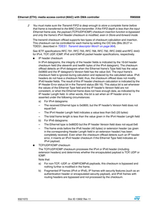
![RM0008 Ethernet (ETH): media access control (MAC) with DMA controller
The checksum is calculated for the TCP, UDP, or ICMP payload and inserted into its
corresponding field in the header. It can work in the following two modes:
– In the first mode, the TCP, UDP, or ICMPv6 pseudo-header is not included in the
checksum calculation and is assumed to be present in the input frame’s checksum
field. The checksum field is included in the checksum calculation, and then
replaced by the final calculated checksum.
– In the second mode, the checksum field is ignored, the TCP, UDP, or ICMPv6
pseudo-header data are included into the checksum calculation, and the
checksum field is overwritten with the final calculated value.
Note that: for ICMP-over-IPv4 packets, the checksum field in the ICMP packet must
always be 0x0000 in both modes, because pseudo-headers are not defined for such
packets. If it does not equal 0x0000, an incorrect checksum may be inserted into the
packet.
The result of this operation is indicated by the payload checksum error status bit in the
Transmit Status vector (bit 12). The payload checksum error status bit is set when
either of the following is detected:
– the frame has been forwarded to the MAC transmitter in Store-and-forward mode
without the end of frame being written to the FIFO
– the packet ends before the number of bytes indicated by the payload length field in
the IP header is received.
When the packet is longer than the indicated payload length, the bytes are ignored as
stuff bytes, and no error is reported. When the first type of error is detected, the TCP,
UDP or ICMP header is not modified. For the second error type, still, the calculated
checksum is inserted into the corresponding header field.
MII/RMII transmit bit order
Each nibble from the MII is transmitted on the RMII a dibit at a time with the order of dibit
transmission shown in Figure 337. Lower order bits (D1 and D0) are transmitted first
followed by higher order bits (D2 and D3).
Figure 337. Transmission bit order
RMII_TXD[1:0]
LSB MSB
D0 D1 Bibit stream
LSB D0
D1
MII_TXD[3:0]
D2
MSB D3
Nibble stream ai15632
Doc ID 13902 Rev 11 933/1072](https://image.slidesharecdn.com/stm32referencemanual-110220082754-phpapp01/85/Stm32-reference-manual-933-320.jpg)
![Ethernet (ETH): media access control (MAC) with DMA controller RM0008
MII/RMII transmit timing diagrams
Figure 338. Transmission with no collision
MII_TX_CLK
MII_TX_EN
MII_TXD[3:0] PR EA MB LE
MII_CS
MII_COL
Low
ai15631
Figure 339. Transmission with collision
MII_TX_CLK
MII_TX_EN
MII_TXD[3:0] PR EAM BLE SFD DA DA JAM JAM JAM JAM
MII_CS
MII_COL
ai15651
Figure 340 shows a frame transmission in MII and RMII.
934/1072 Doc ID 13902 Rev 11](https://image.slidesharecdn.com/stm32referencemanual-110220082754-phpapp01/85/Stm32-reference-manual-934-320.jpg)
![RM0008 Ethernet (ETH): media access control (MAC) with DMA controller
Figure 340. Frame transmission in MMI and RMII modes
MII_RX_CLK
MII_TX_EN
MII_TXD[3:0]
RMII_REF_CLK
RMII_TX_EN
RMII_TXD[1:0]
ai15652
28.5.3 MAC frame reception
The MAC received frames are pushes into the Rx FIFO. The status (fill level) of this FIFO is
indicated to the DMA once it crosses the configured receive threshold (RTC in the
ETH_DMAOMR register) so that the DMA can initiate pre-configured burst transfers towards
the AHB interface.
In the default Cut-through mode, when 64 bytes (configured with the RTC bits in the
ETH_DMAOMR register) or a full packet of data are received into the FIFO, the data are
popped out and the DMA is notified of its availability. Once the DMA has initiated the transfer
to the AHB interface, the data transfer continues from the FIFO until a complete packet has
been transferred. Upon completion of the EOF frame transfer, the status word is popped out
and sent to the DMA controller.
In Rx FIFO Store-and-forward mode (configured by the RSF bit in the ETH_DMAOMR
register), a frame is read out only after being written completely into the Receive FIFO. In
this mode, all error frames are dropped (if the core is configured to do so) such that only
valid frames are read out and forwarded to the application. In Cut-through mode, some error
frames are not dropped, because the error status is received at the end of the frame, by
which time the start of that frame has already been read out of the FIFO.
A receive operation is initiated when the MAC detects an SFD on the MII. The core strips the
preamble and SFD before proceeding to process the frame. The header fields are checked
for the filtering and the FCS field used to verify the CRC for the frame. The frame is dropped
in the core if it fails the address filter.
Receive protocol
The received frame preamble and SFD are stripped. Once the SFD has been detected, the
MAC starts sending the Ethernet frame data to the receive FIFO, beginning with the first
byte following the SFD (destination address). If IEEE 1588 time stamping is enabled, a
snapshot of the system time is taken when any frame's SFD is detected on the MII. Unless
the MAC filters out and drops the frame, this time stamp is passed on to the application.
Doc ID 13902 Rev 11 935/1072](https://image.slidesharecdn.com/stm32referencemanual-110220082754-phpapp01/85/Stm32-reference-manual-935-320.jpg)


![Ethernet (ETH): media access control (MAC) with DMA controller RM0008
Meanwhile, if another Pause frame is detected with a zero Pause time value, the MAC
resets the Pause time and manages this new pause request.
If the received control frame matches neither the type field (0x8808), the opcode (0x00001),
nor the byte length (64 bytes), or if there is a CRC error, the MAC does not generate a
Pause.
In the case of a pause frame with a multicast destination address, the MAC filters the frame
based on the address match.
For a pause frame with a unicast destination address, the MAC filtering depends on whether
the DA matched the contents of the MAC address 0 register and whether the UPDF bit in
ETH_MACFCR is set (detecting a pause frame even with a unicast destination address).
The PCF register bits (bits [7:6] in ETH_MACFFR) control filtering for control frames in
addition to address filtering.
Receive operation multiframe handling
Since the status is available immediately following the data, the FIFO is capable of storing
any number of frames into it, as long as it is not full.
Error handling
If the Rx FIFO is full before it receives the EOF data from the MAC, an overflow is declared
and the whole frame is dropped, and the overflow counter in the (ETH_DMAMFBOCR
register) is incremented. The status indicates a partial frame due to overflow. The Rx FIFO
can filter error and undersized frames, if enabled (using the FEF and FUGF bits in
ETH_DMAOMR).
If the Receive FIFO is configured to operate in Store-and-forward mode, all error frames can
be filtered and dropped.
In Cut-through mode, if a frame's status and length are available when that frame's SOF is
read from the Rx FIFO, then the complete erroneous frame can be dropped. The DMA can
flush the error frame being read from the FIFO, by enabling the receive frame flash bit. The
data transfer to the application (DMA) is then stopped and the rest of the frame is internally
read and dropped. The next frame transfer can then be started, if available.
Receive status word
At the end of the Ethernet frame reception, the MAC outputs the receive status to the
application (DMA). The detailed description of the receive status is the same as for
bits[31:0] in RDES0, given in RDES0: Receive descriptor Word0 on page 973.
Frame length interface
In case of switch applications, data transmission and reception between the application and
MAC happen as complete frame transfers. The application layer should be aware of the
length of the frames received from the ingress port in order to transfer the frame to the
egress port. The MAC core provides the frame length of each received frame inside the
status at the end of each frame reception.
Note: A frame length value of 0 is given for partial frames written into the Rx FIFO due to overflow.
MII/RMII receive bit order
Each nibble is transmitted to the MII from the dibit received from the RMII in the nibble
transmission order shown in Figure 341. The lower-order bits (D0 and D1) are received first,
followed by the higher-order bits (D2 and D3).
938/1072 Doc ID 13902 Rev 11](https://image.slidesharecdn.com/stm32referencemanual-110220082754-phpapp01/85/Stm32-reference-manual-938-320.jpg)
![RM0008 Ethernet (ETH): media access control (MAC) with DMA controller
Figure 341. Receive bit order
RMII_RXD[1:0]
LSB MSB
D0 D1 Di-bit stream
LSB D0
D1
MII_RXD[3:0]
D2
MSB D3
Nibble stream ai15633
Figure 342. Reception with no error
MII_RX_CLK
MII_RX_DV
MII_RXD[3:0] PREAMBLE SFD FCS
MII_RX_ERR
ai15634
Figure 343. Reception with errors
MII_RX_CLK
MII_RX_DV
MII_RXD[3:0] PREAMBLE SFD DA DA XX XX XX
MII_RX_ERR
ai15635
Doc ID 13902 Rev 11 939/1072](https://image.slidesharecdn.com/stm32referencemanual-110220082754-phpapp01/85/Stm32-reference-manual-939-320.jpg)
![Ethernet (ETH): media access control (MAC) with DMA controller RM0008
Figure 344. Reception with false carrier indication
MII_RX_CLK
MII_RX_DV
MII_RXD[3:0] XX XX XX XX 0E XX XX XX XX
MII_RX_ERR
ai15636
28.5.4 MAC interrupts
Interrupts can be generated from the MAC core as a result of various events.
The ETH_MACSR register describes the events that can cause an interrupt from the MAC
core. You can prevent each event from asserting the interrupt by setting the corresponding
mask bits in the Interrupt Mask register.
The interrupt register bits only indicate the block from which the event is reported. You have
to read the corresponding status registers and other registers to clear the interrupt. For
example, bit 3 of the Interrupt register, set high, indicates that the Magic packet or Wake-on-
LAN frame is received in Power-down mode. You must read the ETH_MACPMTCSR
Register to clear this interrupt event.
Figure 345. MAC core interrupt masking scheme
TSTS
TSTI
AND
TSTIM
Interrupt
OR
PMTS
PMTI
AND
PMTIM
ai15637
28.5.5 MAC filtering
Address filtering
Address filtering checks the destination and source addresses on all received frames and
the address filtering status is reported accordingly. Address checking is based on different
parameters (Frame filter register) chosen by the application. The filtered frame can also be
identified: multicast or broadcast frame.
Address filtering uses the station's physical (MAC) address and the Multicast Hash table for
address checking purposes.
940/1072 Doc ID 13902 Rev 11](https://image.slidesharecdn.com/stm32referencemanual-110220082754-phpapp01/85/Stm32-reference-manual-940-320.jpg)

![Ethernet (ETH): media access control (MAC) with DMA controller RM0008
Broadcast address filter
The MAC does not filter any broadcast frames in the default mode. However, if the MAC is
programmed to reject all broadcast frames by setting the BFD bit in the Frame filter register,
any broadcast frames are dropped.
Unicast source address filter
The MAC can also perform perfect filtering based on the source address field of the received
frames. By default, the MAC compares the SA field with the values programmed in the SA
registers. The MAC address registers [1:3] can be configured to contain SA instead of DA
for comparison, by setting bit 30 in the corresponding register. Group filtering with SA is also
supported. The frames that fail the SA filter are dropped by the MAC if the SAF bit in the
Frame filter register is set. Otherwise, the result of the SA filter is given as a status bit in the
Receive Status word (see RDES0: Receive descriptor Word0).
When the SAF bit is set, the result of the SA and DA filters is AND’ed to decide whether the
frame needs to be forwarded. This means that either of the filter fail result will drop the
frame. Both filters have to pass the frame for the frame to be forwarded to the application.
Inverse filtering operation
For both destination and source address filtering, there is an option to invert the filter-match
result at the final output. These are controlled by the DAIF and SAIF bits in the Frame filter
register, respectively. The DAIF bit is applicable for both Unicast and Multicast DA frames.
The result of the unicast/multicast destination address filter is inverted in this mode.
Similarly, when the SAIF bit is set, the result of the unicast SA filter is inverted. Table 209
and Table 210 summarize destination and source address filtering based on the type of
frame received.
Table 209. Destination address filtering table
Frame
PM HPF HU DAIF HM PAM DB DA filter operation
type
1 X X X X X X Pass
Broadcast 0 X X X X X 0 Pass
0 X X X X X 1 Fail
1 X X X X X X Pass all frames
0 X 0 0 X X X Pass on perfect/group filter match
0 X 0 1 X X X Fail on perfect/Group filter match
0 0 1 0 X X X Pass on hash filter match
Unicast
0 0 1 1 X X X Fail on hash filter match
Pass on hash or perfect/Group filter
0 1 1 0 X X X
match
0 1 1 1 X X X Fail on hash or perfect/Group filter match
942/1072 Doc ID 13902 Rev 11](https://image.slidesharecdn.com/stm32referencemanual-110220082754-phpapp01/85/Stm32-reference-manual-942-320.jpg)


![RM0008 Ethernet (ETH): media access control (MAC) with DMA controller
wakeup frame filter register to reach the last register. Each read/write points the wakeup
frame filter register to the next filter register.
Figure 346. Wakeup frame filter register
Wakeup frame filter reg0 Filter 0 Byte Mask
Wakeup frame filter reg1 Filter 1 Byte Mask
Wakeup frame filter reg2 Filter 2 Byte Mask
Wakeup frame filter reg3 Filter 3 Byte Mask
Filter 3 Filter 2 Filter 1 Filter 0
Wakeup frame filter reg4 RSVD
Command
RSVD
Command
RSVD
Command
RSVD
Command
Wakeup frame filter reg5 Filter 3 Offset Filter 2 Offset Filter 1 Offset Filter 0 Offset
Wakeup frame filter reg6 Filter 1 CRC - 16 Filter 0 CRC - 16
Wakeup frame filter reg7 Filter 3 CRC - 16 Filter 2 CRC - 16
ai15647
● Filter i Byte Mask
This register defines which bytes of the frame are examined by filter i (0, 1, 2, and 3) in
order to determine whether or not the frame is a wakeup frame. The MSB (thirty-first
bit) must be zero. Bit j [30:0] is the Byte Mask. If bit j (byte number) of the Byte Mask is
set, then Filter i Offset + j of the incoming frame is processed by the CRC block;
otherwise Filter i Offset + j is ignored.
● Filter i Command
This 4-bit command controls the filter i operation. Bit 3 specifies the address type,
defining the pattern’s destination address type. When the bit is set, the pattern applies
to only multicast frames. When the bit is reset, the pattern applies only to unicast
frames. Bit 2 and bit 1 are reserved. Bit 0 is the enable bit for filter i; if bit 0 is not set,
filter i is disabled.
● Filter i Offset
This register defines the offset (within the frame) from which the frames are examined
by filter i. This 8-bit pattern offset is the offset for the filter i first byte to be examined.
The minimum allowed is 12, which refers to the 13th byte of the frame (offset value 0
refers to the first byte of the frame).
● Filter i CRC-16
This register contains the CRC_16 value calculated from the pattern, as well as the
byte mask programmed to the wakeup filter register block.
Remote wakeup frame detection
When the MAC is in sleep mode and the remote wakeup bit is enabled in the
ETH_MACPMTCSR register, normal operation is resumed after receiving a remote wakeup
frame. The application writes all eight wakeup filter registers, by performing a sequential
write to the wakeup frame filter register address. The application enables remote wakeup by
writing a 1 to bit 2 in the ETH_MACPMTCSR register. PMT supports four programmable
filters that provide different receive frame patterns. If the incoming frame passes the address
filtering of Filter Command, and if Filter CRC-16 matches the incoming examined pattern,
then the wakeup frame is received. Filter_offset (minimum value 12, which refers to the 13th
byte of the frame) determines the offset from which the frame is to be examined. Filter Byte
Doc ID 13902 Rev 11 945/1072](https://image.slidesharecdn.com/stm32referencemanual-110220082754-phpapp01/85/Stm32-reference-manual-945-320.jpg)

![RM0008 Ethernet (ETH): media access control (MAC) with DMA controller
1. Disable the transmit DMA and wait for any previous frame transmissions to complete.
These transmissions can be detected when the transmit interrupt ETH_DMASR
register[0] is received.
2. Disable the MAC transmitter and MAC receiver by clearing the RE and TE bits in the
ETH_MACCR configuration register.
3. Wait for the receive DMA to have emptied all the frames in the Rx FIFO.
4. Disable the receive DMA.
5. Configure and enable the EXTI line 19 to generate either an event or an interrupt.
6. If you configure the EXTI line 19 to generate an interrupt, you also have to correctly
configure the ETH_WKUP_IRQ Handler function, which should clear the pending bit of
the EXTI line 19.
7. Enable Magic packet/Wake-on-LAN frame detection by setting the MFE/ WFE bit in the
ETH_MACPMTCSR register.
8. Enable the MAC power-down mode, by setting the PD bit in the ETH_MACPMTCSR
register.
9. Enable the MAC Receiver by setting the RE bit in the ETH_MACCR register.
10. Enter the system’s Stop mode (for more details refer to Section 4.3.4: Stop mode):
11. On receiving a valid wakeup frame, the Ethernet peripheral exits the power-down
mode.
12. Read the ETH_MACPMTCSR to clear the power management event flag, enable the
MAC transmitter state machine, and the receive and transmit DMA.
13. Configure the system clock: enable the HSE and set the clocks.
28.5.9 Precision time protocol (IEEE1588 PTP)
The IEEE 1588 standard defines a protocol that allows precise clock synchronization in
measurement and control systems implemented with technologies such as network
communication, local computing and distributed objects. The protocol applies to systems
that communicate by local area networks supporting multicast messaging, including (but not
limited to) Ethernet. This protocol is used to synchronize heterogeneous systems that
include clocks of varying inherent precision, resolution and stability. The protocol supports
system-wide synchronization accuracy in the submicrosecond range with minimum network
and local clock computing resources. The message-based protocol, known as the precision
time protocol (PTP), is transported over UDP/IP. The system or network is classified into
Master and Slave nodes for distributing the timing/clock information. The protocol’s
technique for synchronizing a slave node to a master node by exchanging PTP messages is
described in Figure 347.
Doc ID 13902 Rev 11 947/1072](https://image.slidesharecdn.com/stm32referencemanual-110220082754-phpapp01/85/Stm32-reference-manual-947-320.jpg)


![RM0008 Ethernet (ETH): media access control (MAC) with DMA controller
PTP pulse-per-second output signal
This PTP pulse output is used to check the synchronization between all nodes in the
network. To be able to test the difference between the local slave clock and the master
reference clock, both clocks were given a pulse-per-second (PPS) output signal that may be
connected to an oscilloscope if necessary. The deviation between the two signals can
therefore be measured. The pulse width of the PPS output is 125 ms.
The PPS output is enabled through bit 30 in the AFIO_MAPR register.
Figure 350. PPS output
PPS output
Ethernet MAC
ai15672
28.6 Ethernet functional description: DMA controller operation
The DMA has independent transmit and receive engines, and a CSR space. The transmit
engine transfers data from system memory into the Tx FIFO while the receive engine
transfers data from the Rx FIFO into system memory. The controller utilizes descriptors to
efficiently move data from source to destination with minimum CPU intervention. The DMA
is designed for packet-oriented data transfers such as frames in Ethernet. The controller can
be programmed to interrupt the CPU in cases such as frame transmit and receive transfer
completion, and other normal/error conditions. The DMA and the STM32F107xx
communicate through two data structures:
● Control and status registers (CSR)
● Descriptor lists and data buffers.
Control and status registers are described in detail in Section 28.8 on page 981. Descriptors
are described in detail in Section on page 961.
The DMA transfers the received data frames to the receive buffer in the STM32F107xx
memory, and transmits data frames from the transmit buffer in the STM32F107xx memory.
Descriptors that reside in the STM32F107xx memory act as pointers to these buffers. There
are two descriptor lists: one for reception, and one for transmission. The base address of
each list is written into DMA Registers 3 and 4, respectively. A descriptor list is forward-
linked (either implicitly or explicitly). The last descriptor may point back to the first entry to
create a ring structure. Explicit chaining of descriptors is accomplished by configuring the
second address chained in both the receive and transmit descriptors (RDES1[14] and
TDES0[20]). The descriptor lists reside in the Host’s physical memory space. Each
descriptor can point to a maximum of two buffers. This enables the use of two physically
addressed buffers, instead of two contiguous buffers in memory. A data buffer resides in the
Host’s physical memory space, and consists of an entire frame or part of a frame, but cannot
exceed a single frame. Buffers contain only data. The buffer status is maintained in the
descriptor. Data chaining refers to frames that span multiple data buffers. However, a single
descriptor cannot span multiple frames. The DMA skips to the next frame buffer when the
end of frame is detected. Data chaining can be enabled or disabled. The descriptor ring and
chain structure is shown in Figure 351.
Doc ID 13902 Rev 11 953/1072](https://image.slidesharecdn.com/stm32referencemanual-110220082754-phpapp01/85/Stm32-reference-manual-953-320.jpg)
![Ethernet (ETH): media access control (MAC) with DMA controller RM0008
Figure 351. Descriptor ring and chain structure
Ring structure Chain structure
Buffer 1 Buffer 1
Descriptor 0 Descriptor 0
Buffer 2
Buffer 1
Descriptor 1
Buffer 2 Buffer 1
Descriptor 1
Buffer 1
Descriptor 2
Buffer 2
Descriptor 2 Buffer 1
Buffer 1
Descriptor n
Buffer 2
Next descriptor
ai15638
28.6.1 Initialization of a transfer using DMA
Initialization for the MAC is as follows:
1. Write to ETH_DMABMR to set STM32F107xx bus access parameters.
2. Write to the ETH_DMAIER register to mask unnecessary interrupt causes.
3. The software driver creates the transmit and receive descriptor lists. Then it writes to
both the ETH_DMARDLAR and ETH_DMATDLAR registers, providing the DMA with
the start address of each list.
4. Write to MAC Registers 1, 2, and 3 to choose the desired filtering options.
5. Write to the MAC ETH_MACCR register to configure and enable the transmit and
receive operating modes. The PS and DM bits are set based on the auto-negotiation
result (read from the PHY).
6. Write to the ETH_DMAOMR register to set bits 13 and 1 and start transmission and
reception.
7. The transmit and receive engines enter the running state and attempt to acquire
descriptors from the respective descriptor lists. The receive and transmit engines then
begin processing receive and transmit operations. The transmit and receive processes
are independent of each other and can be started or stopped separately.
28.6.2 Host bus burst access
The DMA attempts to execute fixed-length burst transfers on the AHB master interface if
configured to do so (FB bit in ETH_DMABMR). The maximum burst length is indicated and
limited by the PBL field (ETH_DMABMR [13:8]). The receive and transmit descriptors are
always accessed in the maximum possible burst size (limited by PBL) for the 16 bytes to be
read.
The Transmit DMA initiates a data transfer only when there is sufficient space in the
Transmit FIFO to accommodate the configured burst or the number of bytes until the end of
frame (when it is less than the configured burst length). The DMA indicates the start address
and the number of transfers required to the AHB Master Interface. When the AHB Interface
is configured for fixed-length burst, then it transfers data using the best combination of
954/1072 Doc ID 13902 Rev 11](https://image.slidesharecdn.com/stm32referencemanual-110220082754-phpapp01/85/Stm32-reference-manual-954-320.jpg)

![Ethernet (ETH): media access control (MAC) with DMA controller RM0008
databus width. If a descriptor is marked as last, then the buffer may not be full (as indicated
by the buffer size in RDES1). To compute the amount of valid data in this final buffer, the
driver must read the frame length (FL bits in RDES0[29:16]) and subtract the sum of the
buffer sizes of the preceding buffers in this frame. The receive DMA always transfers the
start of next frame with a new descriptor.
Note: Even when the start address of a receive buffer is not aligned to the system databus width
the system should allocate a receive buffer of a size aligned to the system bus width. For
example, if the system allocates a 1024 byte (1 KB) receive buffer starting from address
0x1000, the software can program the buffer start address in the receive descriptor to have
a 0x1002 offset. The receive DMA writes the frame to this buffer with dummy data in the first
two locations (0x1000 and 0x1001). The actual frame is written from location 0x1002. Thus,
the actual useful space in this buffer is 1022 bytes, even though the buffer size is
programmed as 1024 bytes, due to the start address offset.
28.6.5 DMA arbiter
The arbiter inside the DMA takes care of the arbitration between transmit and receive
channel accesses to the AHB master interface. Two types of arbitrations are possible:
round-robin, and fixed-priority. When round-robin arbitration is selected (DA bit in
ETH_DMABMR is reset), the arbiter allocates the databus in the ratio set by the RTPR bits
in ETH_DMABMR, when both transmit and receive DMAs request access simultaneously.
When the DA bit is set, the receive DMA always gets priority over the transmit DMA for data
access.
28.6.6 Error response to DMA
For any data transfer initiated by a DMA channel, if the slave replies with an error response,
that DMA stops all operations and updates the error bits and the fatal bus error bit in the
Status register (ETH_DMASR register). That DMA controller can resume operation only
after soft- or hard-resetting the peripheral and re-initializing the DMA.
28.6.7 Tx DMA configuration
TxDMA operation: default (non-OSF) mode
The transmit DMA engine in default mode proceeds as follows:
1. The user sets up the transmit descriptor (TDES0-TDES3) and sets the OWN bit
(TDES0[31]) after setting up the corresponding data buffer(s) with Ethernet frame data.
2. Once the ST bit (ETH_DMAOMR register[13]) is set, the DMA enters the Run state.
3. While in the Run state, the DMA polls the transmit descriptor list for frames requiring
transmission. After polling starts, it continues in either sequential descriptor ring order
or chained order. If the DMA detects a descriptor flagged as owned by the CPU, or if an
error condition occurs, transmission is suspended and both the Transmit Buffer
956/1072 Doc ID 13902 Rev 11](https://image.slidesharecdn.com/stm32referencemanual-110220082754-phpapp01/85/Stm32-reference-manual-956-320.jpg)
![RM0008 Ethernet (ETH): media access control (MAC) with DMA controller
Unavailable (ETH_DMASR register[2]) and Normal Interrupt Summary (ETH_DMASR
register[16]) bits are set. The transmit engine proceeds to Step 9.
4. If the acquired descriptor is flagged as owned by DMA (TDES0[31] is set), the DMA
decodes the transmit data buffer address from the acquired descriptor.
5. The DMA fetches the transmit data from the STM32F107xx memory and transfers the
data.
6. If an Ethernet frame is stored over data buffers in multiple descriptors, the DMA closes
the intermediate descriptor and fetches the next descriptor. Steps 3, 4, and 5 are
repeated until the end of Ethernet frame data is transferred.
7. When frame transmission is complete, if IEEE 1588 time stamping was enabled for the
frame (as indicated in the transmit status) the time stamp value is written to the transmit
descriptor (TDES2 and TDES3) that contains the end-of-frame buffer. The status
information is then written to this transmit descriptor (TDES0). Because the OWN bit is
cleared during this step, the CPU now owns this descriptor. If time stamping was not
enabled for this frame, the DMA does not alter the contents of TDES2 and TDES3.
8. Transmit Interrupt (ETH_DMASR register [0]) is set after completing the transmission of
a frame that has Interrupt on Completion (TDES1[31]) set in its last descriptor. The
DMA engine then returns to Step 3.
9. In the Suspend state, the DMA tries to re-acquire the descriptor (and thereby returns to
Step 3) when it receives a transmit poll demand, and the Underflow Interrupt Status bit
is cleared.
Figure 352 shows the TxDMA transmission flow in default mode.
Doc ID 13902 Rev 11 957/1072](https://image.slidesharecdn.com/stm32referencemanual-110220082754-phpapp01/85/Stm32-reference-manual-957-320.jpg)
![Ethernet (ETH): media access control (MAC) with DMA controller RM0008
Figure 352. TxDMA operation in Default mode
Start TxDMA Start Stop TxDMA
(Re-)fetch next
descriptor
Poll demand (AHB) Yes
error?
No
TxDMA suspended No
Own
bit set?
Yes
Transfer data from
buffer(s)
(AHB) Yes
error?
No
No
Frame xfer
complete?
Yes
Close intermediate
descriptor Wait for Tx status
Time stamp Yes Write time stamp to
present? TDES2 and TDES3
No
Write status word No
(AHB) Yes
to TDES0 error?
No
(AHB) Yes
error?
ai15639
TxDMA operation: OSF mode
While in the Run state, the transmit process can simultaneously acquire two frames without
closing the Status descriptor of the first (if the OSF bit is set in ETH_DMAOMR register[2]).
As the transmit process finishes transferring the first frame, it immediately polls the transmit
descriptor list for the second frame. If the second frame is valid, the transmit process
transfers this frame before writing the first frame’s status information. In OSF mode, the
Run-state transmit DMA operates according to the following sequence:
958/1072 Doc ID 13902 Rev 11](https://image.slidesharecdn.com/stm32referencemanual-110220082754-phpapp01/85/Stm32-reference-manual-958-320.jpg)

![Ethernet (ETH): media access control (MAC) with DMA controller RM0008
Figure 353. TxDMA operation in OSF mode
Start TxDMA Start Stop TxDMA
(Re-)fetch next
descriptor
(AHB) Yes
Poll error?
demand
No
TxDMA suspended No Own
bit set?
Yes
Previous frame
status available Transfer data from
buffer(s)
Time stamp (AHB) Yes
present? error?
No No
Yes
No Frame xfer Second
Write time stamp to Yes
complete? frame?
TDES2 & TDES3 No
for previous frame Yes
Close intermediate Wait for previous
descriptor frame’s Tx status
(AHB) Yes
Write time stamp to
error? Time stamp Yes TDES2 & TDES3
present? for previous frame
No
No
Write status word to Write status word to No
(AHB) Yes
prev. frame’s TDES0 prev. frame’s TDES0 error?
(AHB) No (AHB)
No
error? error?
Yes
Yes
ai15640
Transmit frame processing
The transmit DMA expects that the data buffers contain complete Ethernet frames,
excluding preamble, pad bytes, and FCS fields. The DA, SA, and Type/Len fields contain
valid data. If the transmit descriptor indicates that the MAC core must disable CRC or pad
insertion, the buffer must have complete Ethernet frames (excluding preamble), including
the CRC bytes. Frames can be data-chained and span over several buffers. Frames have to
be delimited by the first descriptor (TDES0[28]) and the last descriptor (TDES0[29]). As the
transmission starts, TDES0[28] has to be set in the first descriptor. When this occurs, the
frame data are transferred from the memory buffer to the Transmit FIFO. Concurrently, if the
last descriptor (TDES0[29]) of the current frame is cleared, the transmit process attempts to
acquire the next descriptor. The transmit process expects TDES0[28] to be cleared in this
descriptor. If TDES0[29] is cleared, it indicates an intermediary buffer. If TDES0[29] is set, it
960/1072 Doc ID 13902 Rev 11](https://image.slidesharecdn.com/stm32referencemanual-110220082754-phpapp01/85/Stm32-reference-manual-960-320.jpg)
![RM0008 Ethernet (ETH): media access control (MAC) with DMA controller
indicates the last buffer of the frame. After the last buffer of the frame has been transmitted,
the DMA writes back the final status information to the transmit descriptor 0 (TDES0) word
of the descriptor that has the last segment set in transmit descriptor 0 (TDES0[29]). At this
time, if Interrupt on Completion (TDES0[30]) is set, Transmit Interrupt (in ETH_DMASR
register [0]) is set, the next descriptor is fetched, and the process repeats. Actual frame
transmission begins after the Transmit FIFO has reached either a programmable transmit
threshold (ETH_DMAOMR register[16:14]), or a full frame is contained in the FIFO. There is
also an option for the Store and forward mode (ETH_DMAOMR register[21]). Descriptors
are released (OWN bit TDES0[31] is cleared) when the DMA finishes transferring the frame.
Transmit polling suspended
Transmit polling can be suspended by either of the following conditions:
● The DMA detects a descriptor owned by the CPU (TDES0[31]=0) and the Transmit
buffer unavailable flag is set (ETH_DMASR register[2]). To resume, the driver must give
descriptor ownership to the DMA and then issue a Poll Demand command.
● A frame transmission is aborted when a transmit error due to underflow is detected.
The appropriate Transmit Descriptor 0 (TDES0) bit is set. If the second condition
occurs, both the Abnormal Interrupt Summary (in ETH_DMASR register [15]) and
Transmit Underflow bits (in ETH_DMASR register[5]) are set, and the information is
written to Transmit Descriptor 0, causing the suspension. If the DMA goes into Suspend
state due to the first condition, then both the Normal Interrupt Summary (ETH_DMASR
register [16]) and Transmit Buffer Unavailable (ETH_DMASR register[2]) bits are set. In
both cases, the position in the transmit list is retained. The retained position is that of
the descriptor following the last descriptor closed by the DMA. The driver must explicitly
issue a Transmit Poll Demand command after rectifying the suspension cause.
Tx DMA descriptors
The descriptor structure consists of four 32-bit words as shown in Figure 354. The bit
descriptions of TDES0, TDES1, TDES2 and TDES3 are given below.
Figure 354. Transmit descriptor
31 0
O T T
Ctrl T Res. Ctrl Reserved T
TDES 0 W Status [16:0]
[30:26] S 24 [23:20] [19:18] S
N
E S
TDES 1 Reserved Buffer 2 byte count Reserved Buffer 1 byte count
[31:29] [28:16] [15:13] [12:0]
TDES 2 Buffer 1 address [31:0] / Time stamp low [31:0]
TDES 3 Buffer 2 address [31:0] or Next descriptor address [31:0] / Time stamp high [31:0]
ai15642b
Doc ID 13902 Rev 11 961/1072](https://image.slidesharecdn.com/stm32referencemanual-110220082754-phpapp01/85/Stm32-reference-manual-961-320.jpg)
![Ethernet (ETH): media access control (MAC) with DMA controller RM0008
● TDES0: Transmit descriptor Word0
The application software has to program the control bits [30:26]+[23:20] plus the OWN
bit [31] during descriptor initialization. When the DMA updates the descriptor (or writes
it back), it resets all the control bits plus the OWN bit, and reports only the status bits.
31 30 29 28 27 26 25 24 23 22 21 20 19 18 17 16 15 14 13 12 11 10 9 8 7 6 5 4 3 2 1 0
O
TT TE TC TT IH IP LC LC
W IC LS FS DC DP CIC ES JT FF NC EC VF CC ED UF DB
SE Res R H Res. SS E E A O
N
rw rw rw rw rw rw rw rw rw rw rw rw rw rw rw rw rw rw rw rw rw rw rw rw rw rw rw rw rw
Bit 31 OWN: Own bit
When set, this bit indicates that the descriptor is owned by the DMA. When this bit is reset, it
indicates that the descriptor is owned by the CPU. The DMA clears this bit either when it
completes the frame transmission or when the buffers allocated in the descriptor are read
completely. The ownership bit of the frame’s first descriptor must be set after all subsequent
descriptors belonging to the same frame have been set.
Bit 30 IC: Interrupt on completion
When set, this bit sets the Transmit Interrupt (Register 5[0]) after the present frame has been
transmitted.
Bit 29 LS: Last segment
When set, this bit indicates that the buffer contains the last segment of the frame.
Bit 28 FS: First segment
When set, this bit indicates that the buffer contains the first segment of a frame.
Bit 27 DC: Disable CRC
When this bit is set, the MAC does not append a cyclic redundancy check (CRC) to the end of
the transmitted frame. This is valid only when the first segment (TDES0[28]) is set.
Bit 26 DP: Disable pad
When set, the MAC does not automatically add padding to a frame shorter than 64 bytes.
When this bit is reset, the DMA automatically adds padding and CRC to a frame shorter than
64 bytes, and the CRC field is added despite the state of the DC (TDES0[27]) bit. This is valid
only when the first segment (TDES0[28]) is set.
Bit 25 TTSE: Transmit time stamp enable
When TTSE is set and when TSE is set (ETH_PTPTSCR bit 0), IEEE1588 hardware time
stamping is activated for the transmit frame described by the descriptor. This field is only valid
when the First segment control bit (TDES0[28]) is set.
Bit 24 Reserved
Bits 23:22 CIC: Checksum insertion control
These bits control the checksum calculation and insertion. Bit encoding is as shown below:
00: Checksum Insertion disabled
01: Only IP header checksum calculation and insertion are enabled
10: IP header checksum and payload checksum calculation and insertion are enabled, but
pseudo-header checksum is not calculated in hardware
11: IP Header checksum and payload checksum calculation and insertion are enabled, and
pseudo-header checksum is calculated in hardware.
Bit 21 TER: Transmit end of ring
When set, this bit indicates that the descriptor list reached its final descriptor. The DMA returns
to the base address of the list, creating a descriptor ring.
962/1072 Doc ID 13902 Rev 11](https://image.slidesharecdn.com/stm32referencemanual-110220082754-phpapp01/85/Stm32-reference-manual-962-320.jpg)
![RM0008 Ethernet (ETH): media access control (MAC) with DMA controller
Bit 20 TCH: Second address chained
When set, this bit indicates that the second address in the descriptor is the next descriptor
address rather than the second buffer address. When TDES0[20] is set, TBS2 (TDES1[28:16])
is a “don’t care” value. TDES0[21] takes precedence over TDES0[20].
Bits 19:18 Reserved
Bit 17 TTSS: Transmit time stamp status
This field is used as a status bit to indicate that a time stamp was captured for the described
transmit frame. When this bit is set, TDES2 and TDES3 have a time stamp value captured for the
transmit frame. This field is only valid when the descriptor’s Last segment control bit (TDES0[29]) is
set.
Bit 16 IHE: IP header error
When set, this bit indicates that the MAC transmitter detected an error in the IP datagram
header. The transmitter checks the header length in the IPv4 packet against the number of
header bytes received from the application and indicates an error status if there is a mismatch.
For IPv6 frames, a header error is reported if the main header length is not 40 bytes.
Furthermore, the Ethernet length/type field value for an IPv4 or IPv6 frame must match the IP
header version received with the packet. For IPv4 frames, an error status is also indicated if
the Header Length field has a value less than 0x5.
Bit 15 ES: Error summary
Indicates the logical OR of the following bits:
– TDES0[14]: Jabber timeout
– TDES0[13]: Frame flush
– TDES0[11]: Loss of carrier
– TDES0[10]: No carrier
– TDES0[9]: Late collision
– TDES0[8]: Excessive collision
– TDES0[2]:Excessive deferral
– TDES0[1]: Underflow error
– TDES0[16]: IP header error
– TDES0[12]: IP payload error
Bit 14 JT: Jabber timeout
When set, this bit indicates the MAC transmitter has experienced a jabber timeout. This bit is
only set when the MAC configuration register’s JD bit is not set.
Bit 13 FF: Frame flushed
When set, this bit indicates that the DMA/MTL flushed the frame due to a software Flush
command given by the CPU.
Bit 12 IPE: IP payload error
When set, this bit indicates that MAC transmitter detected an error in the TCP, UDP, or ICMP
IP datagram payload. The transmitter checks the payload length received in the IPv4 or IPv6
header against the actual number of TCP, UDP or ICMP packet bytes received from the
application and issues an error status in case of a mismatch.
Bit 11 LCA: Loss of carrier
When set, this bit indicates that a loss of carrier occurred during frame transmission (that is,
the MII_CRS signal was inactive for one or more transmit clock periods during frame
transmission). This is valid only for the frames transmitted without collision when the MAC
operates in Half-duplex mode.
Doc ID 13902 Rev 11 963/1072](https://image.slidesharecdn.com/stm32referencemanual-110220082754-phpapp01/85/Stm32-reference-manual-963-320.jpg)
![Ethernet (ETH): media access control (MAC) with DMA controller RM0008
Bit 10 NC: No carrier
When set, this bit indicates that the Carrier Sense signal form the PHY was not asserted
during transmission.
Bit 9 LCO: Late collision
When set, this bit indicates that frame transmission was aborted due to a collision occurring
after the collision window (64 byte times, including preamble, in MII mode). This bit is not valid
if the Underflow Error bit is set.
Bit 8 EC: Excessive collision
When set, this bit indicates that the transmission was aborted after 16 successive collisions
while attempting to transmit the current frame. If the RD (Disable retry) bit in the MAC
Configuration register is set, this bit is set after the first collision, and the transmission of the
frame is aborted.
Bit 7 VF: VLAN frame
When set, this bit indicates that the transmitted frame was a VLAN-type frame.
Bits 6:3 CC: Collision count
This 4-bit counter value indicates the number of collisions occurring before the frame was
transmitted. The count is not valid when the Excessive collisions bit (TDES0[8]) is set.
Bit 2 ED: Excessive deferral
When set, this bit indicates that the transmission has ended because of excessive deferral of
over 24 288 bit times if the Deferral check (DC) bit in the MAC Control register is set high.
Bit 1 UF: Underflow error
When set, this bit indicates that the MAC aborted the frame because data arrived late from the
RAM memory. Underflow error indicates that the DMA encountered an empty transmit buffer
while transmitting the frame. The transmission process enters the Suspended state and sets
both Transmit underflow (Register 5[5]) and Transmit interrupt (Register 5[0]).
Bit 0 DB: Deferred bit
When set, this bit indicates that the MAC defers before transmission because of the presence
of the carrier. This bit is valid only in Half-duplex mode.
● TDES1: Transmit descriptor Word1
31 30 29 28 27 26 25 24 23 22 21 20 19 18 17 16 15 14 13 12 11 10 9 8 7 6 5 4 3 2 1 0
TBS2 TBS1
Reserved Reserved
rw rw rw rw rw rw rw rw rw rw rw rw rw rw rw rw rw rw rw rw rw rw rw rw rw rw
31:29 Reserved
28:16 TBS2: Transmit buffer 2 size
These bits indicate the second data buffer size in bytes. This field is not valid if TDES0[20] is
set.
15:13 Reserved
12:0 TBS1: Transmit buffer 1 size
These bits indicate the first data buffer byte size, in bytes. If this field is 0, the DMA ignores this
buffer and uses Buffer 2 or the next descriptor, depending on the value of TCH (TDES0[20]).
964/1072 Doc ID 13902 Rev 11](https://image.slidesharecdn.com/stm32referencemanual-110220082754-phpapp01/85/Stm32-reference-manual-964-320.jpg)
![RM0008 Ethernet (ETH): media access control (MAC) with DMA controller
● TDES2: Transmit descriptor Word2
TDES2 contains the address pointer to the first buffer of the descriptor or it contains
time stamp data.
31 30 29 28 27 26 25 24 23 22 21 20 19 18 17 16 15 14 13 12 11 10 9 8 7 6 5 4 3 2 1 0
TBAP1/TTSL
rw
Bits 31:0 TBAP1 / TTSL: Transmit buffer 1 address pointer / Transmit frame time stamp low
These bits take on two different functions: the application uses them to indicate to the DMA the
location of data in memory. And then after transferring all these data, the DMA may then use
these bits to pass back time stamp data.
TBAP: When the software makes this descriptor available to the DMA (at the moment that the
OWN bit is set to 1 in TDES0), these bits indicate the physical address of Buffer 1. There is no
limitation on the buffer address alignment. See Host data buffer alignment on page 955 for further
details on buffer address alignment.
TTSL: Before it clears the OWN bt in TDES0, the DMA updates this field with the 32 least
significant bits of the time stamp captured for the corresponding transmit frame (overwriting the
value for TBAP1). This field has the time stamp only if time stamping is activated for this frame
(see TTSE, TDES0 bit 25) and if the Last segment control bit (LS) in the descriptor is set.
● TDES3: Transmit descriptor Word3
TDES3 contains the address pointer either to the second buffer of the descriptor or the
next descriptor, or it contains time stamp data.
31 30 29 28 27 26 25 24 23 22 21 20 19 18 17 16 15 14 13 12 11 10 9 8 7 6 5 4 3 2 1 0
TBAP2/TTSH
rw
Bits 31:0 TBAP2 / TTSH: Transmit buffer 2 address pointer (Next descriptor address) / Transmit frame
time stamp high
These bits take on two different functions: the application uses them to indicate to the DMA the
location of data in memory. And then after transferring all these data, the DMA may then use
these bits to pass back time stamp data.
TBAP2: When the software makes this descriptor available to the DMA (at the moment when
the OWN bit is set to 1 in TDES0), these bits indicate the physical address of Buffer 2 when a
descriptor ring structure is used. If the Second address chained (TDES1 [24]) bit is set, this
address contains the pointer to the physical memory where the next descriptor is present. The buffer
address pointer must be aligned to the bus width only when TDES1 [24] is set. (LSBs are ignored
internally.)
TTSH: Before it clears the OWN bit in TDES0, the DMA updates this field with the 32 most
significant bits of the time stamp captured for the corresponding transmit frame (overwriting the
value for TBAP2). This field has the time stamp only if time stamping is activated for this frame
(see TDES0 bit 25, TTSE) and if the Last segment control bit (LS) in the descriptor is set.
Tx DMA descriptor format with IEEE1588 time stamp
The descriptor format (as described previously) and field descriptions remain unchanged
when created by software (OWN bit is set in TDES0). However, if the software has enabled
Doc ID 13902 Rev 11 965/1072](https://image.slidesharecdn.com/stm32referencemanual-110220082754-phpapp01/85/Stm32-reference-manual-965-320.jpg)
![Ethernet (ETH): media access control (MAC) with DMA controller RM0008
the IEEE 1588 functionality, the TDES2 and TDES3 descriptor fields take on a different
meaning when the DMA closes the descriptor (OWN bit in TDES0 is cleared).
The Transmit descriptor has additional control and status bits (TTSE and TTSS,
respectively) for time stamping, as shown in Figure 355. The software sets the TTSE bit
(when the OWN bit is set), instructing the core to generate a time stamp for the
corresponding Ethernet frame being transmitted. The DMA sets the TTSS bit if the time
stamp has been updated in the TDES2 and TDES3 fields when the descriptor is closed
(OWN bit is cleared).
Figure 355. Transmit descriptor field format with IEEE1588 time stamp enabled
31 0
O T T
Ctrl T Res. Ctrl Reserved T
TDES 0 W Status [16:0]
[30:26] S 24 [23:20] [19:18] S
N
E S
TDES 1 Reserved Buffer 2 byte count Reserved Buffer 1 byte count
[31:29] [28:16] [15:13] [12:0]
TDES 2 Buffer 1 address [31:0] / Time stamp low [31:0](1)
TDES 3 Buffer 2 address [31:0] or Next descriptor address [31:0] / Time stamp high [31:0](1)
ai15642
1. The DMA updates TDES2 and TDES3 with the time stamp value before clearing the OWN bit in TDES0:
TDES2 is updated with the lower 32 time stamp bits (the sub-second field, called TTSL in subsequent
section TDES2: Transmit descriptor Word2) and TDES3 is updated with the upper 32 time stamp bits (the
Seconds field, called TTSH in subsequent sections TDES3: Transmit descriptor Word3)
966/1072 Doc ID 13902 Rev 11](https://image.slidesharecdn.com/stm32referencemanual-110220082754-phpapp01/85/Stm32-reference-manual-966-320.jpg)
![RM0008 Ethernet (ETH): media access control (MAC) with DMA controller
● TDES0: Transmit descriptor Word0: Transmit time stamp control and status
The value of this field should be preserved by the DMA at the time of closing the
descriptor.
31 30 29 28 27 26 25 24 23 22 21 20 19 18 17 16 15 14 13 12 11 10 9 8 7 6 5 4 3 2 1 0
TTSE
TTSS
OWN
LCO
TCH
TER
LCA
IHE
IC LS FS DC DP CIC ES JT FF IPE NC EC VF CC ED UF DB
Res. Res.
rw rw rw rw rw rw rw rw rw rw rw rw rw rw rw rw rw rw rw rw rw rw rw rw rw rw rw rw rw
Bit 31 OWN: Own bit
When set, this bit indicates that the descriptor is owned by the DMA. When this bit is reset, it
indicates that the descriptor is owned by the CPU. The DMA clears this bit either when it
completes the frame transmission or when the buffers allocated in the descriptor are read
completely. The ownership bit of the frame’s first descriptor must be set after all subsequent
descriptors belonging to the same frame have been set.
Bit 30 IC: Interrupt on completion
When set, this bit sets the Transmit Interrupt (Register 5[0]) after the present frame has been
transmitted.
Bit 29 LS: Last segment
When set, this bit indicates that the buffer contains the last segment of the frame.
Bit 28 FS: First segment
When set, this bit indicates that the buffer contains the first segment of a frame.
Bit 27 DC: Disable CRC
When this bit is set, the MAC does not append a cyclic redundancy check (CRC) to the end of
the transmitted frame. This is valid only when the first segment (TDES0[28]) is set.
Bit 26 DP: Disable pad
When set, the MAC does not automatically add padding to a frame shorter than 64 bytes.
When this bit is reset, the DMA automatically adds padding and CRC to a frame shorter than
64 bytes, and the CRC field is added despite the state of the DC (TDES0[27]) bit. This is valid
only when the first segment (TDES0[28]) is set.
Bit 25 TTSE: Transmit time stamp enable
When set, this field enables IEEE1588 hardware time stamping for the transmit frame described
by the descriptor. This field is only valid when the First segment control bit (TDES0[28]) is set.
Bit 24 Reserved
Bits 23:22 CIC: Checksum insertion control
These bits control the checksum calculation and insertion. Bit encoding is as shown below:
00: Checksum Insertion disabled
01: Only IP header checksum calculation and insertion are enabled
10: IP header checksum and payload checksum calculation and insertion are enabled, but
pseudo-header checksum is not calculated in hardware
11: IP Header checksum and payload checksum calculation and insertion are enabled, and
pseudo-header checksum is calculated in hardware.
Bit 21 TER: Transmit end of ring
When set, this bit indicates that the descriptor list reached its final descriptor. The DMA returns
to the base address of the list, creating a descriptor ring.
Doc ID 13902 Rev 11 967/1072](https://image.slidesharecdn.com/stm32referencemanual-110220082754-phpapp01/85/Stm32-reference-manual-967-320.jpg)
![Ethernet (ETH): media access control (MAC) with DMA controller RM0008
Bit 20 TCH: Second address chained
When set, this bit indicates that the second address in the descriptor is the next descriptor
address rather than the second buffer address. When TDES0[20] is set, TBS2 (TDES1[28:16])
is a “don’t care” value. TDES0[21] takes precedence over TDES0[20].
Bits 19:18 Reserved
Bits 17 TTSS: Transmit time stamp status
This field is used as a status bit to indicate that a time stamp was captured for the described
transmit frame. When this bit is set, TDES2 and TDES3 have a time stamp value captured for the
transmit frame. This field is only valid when the descriptor’s Last segment control bit (TDES0[29]) is
set.
Bit 16 IHE: IP header error
When set, this bit indicates that the MAC transmitter detected an error in the IP datagram
header. The transmitter checks the header length in the IPv4 packet against the number of
header bytes received from the application and indicates an error status if there is a mismatch.
For IPv6 frames, a header error is reported if the main header length is not 40 bytes.
Furthermore, the Ethernet length/type field value for an IPv4 or IPv6 frame must match the IP
header version received with the packet. For IPv4 frames, an error status is also indicated if
the Header Length field has a value less than 0x5.
Bit 15 ES: Error summary
Indicates the logical OR of the following bits:
– TDES0[14]: Jabber timeout
– TDES0[13]: Frame flush
– TDES0[11]: Loss of carrier
– TDES0[10]: No carrier
– TDES0[9]: Late collision
– TDES0[8]: Excessive collision
– TDES0[2]:Excessive deferral
– TDES0[1]: Underflow error
– TDES0[16]: IP header error
– TDES0[12]: IP payload error
Bit 14 JT: Jabber timeout
When set, this bit indicates the MAC transmitter has experienced a jabber timeout. This bit is
only set when the MAC configuration register’s JD bit is not set.
Bit 13 FF: Frame flushed
When set, this bit indicates that the DMA/MTL flushed the frame due to a software Flush
command given by the CPU.
Bit 12 IPE: IP payload error
When set, this bit indicates that MAC transmitter detected an error in the TCP, UDP, or ICMP
IP datagram payload. The transmitter checks the payload length received in the IPv4 or IPv6
header against the actual number of TCP, UDP or ICMP packet bytes received from the
application and issues an error status in case of a mismatch.
Bit 11 LCA: Loss of carrier
When set, this bit indicates that a loss of carrier occurred during frame transmission (that is,
the MII_CRS signal was inactive for one or more transmit clock periods during frame
transmission). This is valid only for the frames transmitted without collision when the MAC
operates in Half-duplex mode.
968/1072 Doc ID 13902 Rev 11](https://image.slidesharecdn.com/stm32referencemanual-110220082754-phpapp01/85/Stm32-reference-manual-968-320.jpg)
![RM0008 Ethernet (ETH): media access control (MAC) with DMA controller
Bit 10 NC: No carrier
When set, this bit indicates that the Carrier Sense signal form the PHY was not asserted
during transmission.
Bit 9 LCO: Late collision
When set, this bit indicates that frame transmission was aborted due to a collision occurring
after the collision window (64 byte times, including preamble, in MII mode). This bit is not valid
if the Underflow Error bit is set.
Bit 8 EC: Excessive collision
When set, this bit indicates that the transmission was aborted after 16 successive collisions
while attempting to transmit the current frame. If the RD (Disable retry) bit in the MAC
Configuration register is set, this bit is set after the first collision, and the transmission of the
frame is aborted.
Bit 7 VF: VLAN frame
When set, this bit indicates that the transmitted frame was a VLAN-type frame.
Bits 6:3 CC: Collision count
This 4-bit counter value indicates the number of collisions occurring before the frame was
transmitted. The count is not valid when the Excessive collisions bit (TDES0[8]) is set.
Bit 2 ED: Excessive deferral
When set, this bit indicates that the transmission has ended because of excessive deferral of
over 24 288 bit times if the Deferral check (DC) bit in the MAC Control register is set high.
Bit 1 UF: Underflow error
When set, this bit indicates that the MAC aborted the frame because data arrived late from the
RAM memory. Underflow error indicates that the DMA encountered an empty transmit buffer
while transmitting the frame. The transmission process enters the Suspended state and sets
both Transmit underflow (Register 5[5]) and Transmit interrupt (Register 5[0]).
Bit 0 DB: Deferred bit
When set, this bit indicates that the MAC defers before transmission because of the presence
of the carrier. This bit is valid only in Half-duplex mode.
● TDES1: Transmit descriptor Word1
Refer to TDES1: Transmit descriptor Word1 section.
● TDES2: Transmit descriptor Word2
31 30 29 28 27 26 25 24 23 22 21 20 19 18 17 16 15 14 13 12 11 10 9 8 7 6 5 4 3 2 1 0
TTSL
rw
Bits 31:0 TTSL: Transmit frame time stamp low
This field is updated by DMA with the 32 least significant bits of the time stamp captured for
the corresponding transmit frame. This field has the time stamp only if the Last segment control bit
(LS) in the descriptor is set.
Doc ID 13902 Rev 11 969/1072](https://image.slidesharecdn.com/stm32referencemanual-110220082754-phpapp01/85/Stm32-reference-manual-969-320.jpg)
![Ethernet (ETH): media access control (MAC) with DMA controller RM0008
● TDES3: Transmit descriptor Word3
31 30 29 28 27 26 25 24 23 22 21 20 19 18 17 16 15 14 13 12 11 10 9 8 7 6 5 4 3 2 1 0
TTSH
rw
Bits 31:0 TTSH: Transmit frame time stamp high
This field is updated by DMA with the 32 most significant bits of the time stamp captured for
the corresponding transmit frame. This field has the time stamp only if the Last segment control bit
(LS) in the descriptor is set.
28.6.8 Rx DMA configuration
The Receive DMA engine’s reception sequence is illustrated in Figure 356 and described
below:
1. The CPU sets up Receive descriptors (RDES0-RDES3) and sets the OWN bit
(RDES0[31]).
2. Once the SR (ETH_DMAOMR register[1]) bit is set, the DMA enters the Run state.
While in the Run state, the DMA polls the receive descriptor list, attempting to acquire
free descriptors. If the fetched descriptor is not free (is owned by the CPU), the DMA
enters the Suspend state and jumps to Step 9.
3. The DMA decodes the receive data buffer address from the acquired descriptors.
4. Incoming frames are processed and placed in the acquired descriptor’s data buffers.
5. When the buffer is full or the frame transfer is complete, the Receive engine fetches the
next descriptor.
6. If the current frame transfer is complete, the DMA proceeds to step 7. If the DMA does
not own the next fetched descriptor and the frame transfer is not complete (EOF is not
yet transferred), the DMA sets the Descriptor error bit in RDES0 (unless flushing is
disabled). The DMA closes the current descriptor (clears the OWN bit) and marks it as
intermediate by clearing the Last segment (LS) bit in the RDES1 value (marks it as last
descriptor if flushing is not disabled), then proceeds to step 8. If the DMA owns the next
descriptor but the current frame transfer is not complete, the DMA closes the current
descriptor as intermediate and returns to step 4.
7. If IEEE 1588 time stamping is enabled, the DMA writes the time stamp (if available) to
the current descriptor’s RDES2 and RDES3. It then takes the received frame’s status
and writes the status word to the current descriptor’s RDES0, with the OWN bit cleared
and the Last segment bit set.
8. The Receive engine checks the latest descriptor’s OWN bit. If the CPU owns the
descriptor (OWN bit is at 0) the Receive buffer unavailable bit (in ETH_DMASR
register[7]) is set and the DMA Receive engine enters the Suspended state (step 9). If
the DMA owns the descriptor, the engine returns to step 4 and awaits the next frame.
9. Before the Receive engine enters the Suspend state, partial frames are flushed from
the Receive FIFO (you can control flushing using bit 24 in the ETH_DMAOMR register).
10. The Receive DMA exits the Suspend state when a Receive Poll demand is given or the
start of next frame is available from the Receive FIFO. The engine proceeds to step 2
and re-fetches the next descriptor.
The DMA does not acknowledge accepting the status until it has completed the time stamp
write-back and is ready to perform status write-back to the descriptor. If software has
970/1072 Doc ID 13902 Rev 11](https://image.slidesharecdn.com/stm32referencemanual-110220082754-phpapp01/85/Stm32-reference-manual-970-320.jpg)

![Ethernet (ETH): media access control (MAC) with DMA controller RM0008
Receive descriptor acquisition
The receive engine always attempts to acquire an extra descriptor in anticipation of an
incoming frame. Descriptor acquisition is attempted if any of the following conditions is/are
satisfied:
● The receive Start/Stop bit (ETH_DMAOMR register[1]) has been set immediately after
the DMA has been placed in the Run state.
● The data buffer of the current descriptor is full before the end of the frame currently
being transferred
● The controller has completed frame reception, but the current receive descriptor has
not yet been closed.
● The receive process has been suspended because of a CPU-owned buffer
(RDES0[31] = 0) and a new frame is received.
● A Receive poll demand has been issued.
Receive frame processing
The MAC transfers the received frames to the STM32F107xx memory only when the frame
passes the address filter and the frame size is greater than or equal to the configurable
threshold bytes set for the Receive FIFO, or when the complete frame is written to the FIFO
in Store-and-forward mode. If the frame fails the address filtering, it is dropped in the MAC
block itself (unless Receive All ETH_MACFFR [31] bit is set). Frames that are shorter than
64 bytes, because of collision or premature termination, can be purged from the Receive
FIFO. After 64 (configurable threshold) bytes have been received, the DMA block begins
transferring the frame data to the receive buffer pointed to by the current descriptor. The
DMA sets the first descriptor (RDES0[9]) after the DMA AHB Interface becomes ready to
receive a data transfer (if DMA is not fetching transmit data from the memory), to delimit the
frame. The descriptors are released when the OWN (RDES0[31]) bit is reset to 0, either as
the data buffer fills up or as the last segment of the frame is transferred to the receive buffer.
If the frame is contained in a single descriptor, both the last descriptor (RDES0[8]) and first
descriptor (RDES0[9]) bits are set. The DMA fetches the next descriptor, sets the last
descriptor (RDES0[8]) bit, and releases the RDES0 status bits in the previous frame
descriptor. Then the DMA sets the receive interrupt bit (ETH_DMASR register [6]). The
same process repeats unless the DMA encounters a descriptor flagged as being owned by
the CPU. If this occurs, the receive process sets the receive buffer unavailable bit
(ETH_DMASR register[7]) and then enters the Suspend state. The position in the receive
list is retained.
Receive process suspended
If a new receive frame arrives while the receive process is in Suspend state, the DMA re-
fetches the current descriptor in the STM32F107xx memory. If the descriptor is now owned
by the DMA, the receive process re-enters the Run state and starts frame reception. If the
descriptor is still owned by the host, by default, the DMA discards the current frame at the
top of the Rx FIFO and increments the missed frame counter. If more than one frame is
stored in the Rx FIFO, the process repeats. The discarding or flushing of the frame at the
top of the Rx FIFO can be avoided by setting the DMA Operation mode register bit 24
(DFRF). In such conditions, the receive process sets the receive buffer unavailable status bit
and returns to the Suspend state.
972/1072 Doc ID 13902 Rev 11](https://image.slidesharecdn.com/stm32referencemanual-110220082754-phpapp01/85/Stm32-reference-manual-972-320.jpg)
![RM0008 Ethernet (ETH): media access control (MAC) with DMA controller
Rx DMA descriptors
The descriptor structure consists of four 32-bit words (16 bytes). These are shown in
Figure 357. The bit descriptions of RDES0, RDES1, RDES2 and RDES3 are given below.
Figure 357. Rx DMA descriptor structure
31 0
O
RDES 0 W Status [30:0]
N
RDES 1 CT Reserved Buffer 2 byte count CTRL Res. Buffer 1 byte count
RL [30:29] [28:16] [15:14] [12:0]
RDES 2 Buffer 1 address [31:0]
RDES 3 Buffer 2 address [31:0] or Next descriptor address [31:0]
ai15644
● RDES0: Receive descriptor Word0
RDES0 contains the received frame status, the frame length and the descriptor
ownership information.
31 30 29 28 27 26 25 24 23 22 21 20 19 18 17 16 15 14 13 12 11 10 9 8 7 6 5 4 3 2 1 0
IPHCE
VLAN
OWN
RWT
AFM
LCO
PCE
SAF
OE
DE
RE
DE
CE
ES
FS
LE
LS
FT
FL
rw
Bit 31 OWN: Own bit
When set, this bit indicates that the descriptor is owned by the DMA of the MAC Subsystem.
When this bit is reset, it indicates that the descriptor is owned by the Host. The DMA clears this bit
either when it completes the frame reception or when the buffers that are associated with this
descriptor are full.
Bit 30 AFM: Destination address filter fail
When set, this bit indicates a frame that failed the DA filter in the MAC Core.
Bits 29:16 FL: Frame length
These bits indicate the byte length of the received frame that was transferred to host memory
(including CRC). This field is valid only when last descriptor (RDES0[8]) is set and descriptor error
(RDES0[14]) is reset.
This field is valid when last descriptor (RDES0[8]) is set. When the last descriptor and error
summary bits are not set, this field indicates the accumulated number of bytes that have been
transferred for the current frame.
Doc ID 13902 Rev 11 973/1072](https://image.slidesharecdn.com/stm32referencemanual-110220082754-phpapp01/85/Stm32-reference-manual-973-320.jpg)
![Ethernet (ETH): media access control (MAC) with DMA controller RM0008
Bit 15 ES: Error summary
Indicates the logical OR of the following bits:
– RDES0[1]: CRC error
– RDES0[3]: Receive error
– RDES0[4]: Watchdog timeout
– RDES0[6]: Late collision
– RDES0[7]: Giant frame (This is not applicable when RDES0[7] indicates an IPV4 header
checksum error.)
– RDES0[11]: Overflow error
– RDES0[14]: Descriptor error.
This field is valid only when the last descriptor (RDES0[8]) is set.
Bit 14 DE: Descriptor error
When set, this bit indicates a frame truncation caused by a frame that does not fit within the current
descriptor buffers, and that the DMA does not own the next descriptor. The frame is truncated. This
field is valid only when the last descriptor (RDES0[8]) is set.
Bit 13 SAF: Source address filter fail
When set, this bit indicates that the SA field of frame failed the SA filter in the MAC Core.
Bit 12 LE: Length error
When set, this bit indicates that the actual length of the received frame does not match the value in
the Length/ Type field. This bit is valid only when the Frame type (RDES0[5]) bit is reset.
Bit 11 OE: Overflow error
When set, this bit indicates that the received frame was damaged due to buffer overflow.
Bit 10 VLAN: VLAN tag
When set, this bit indicates that the frame pointed to by this descriptor is a VLAN frame tagged by
the MAC core.
Bit 9 FS: First descriptor
When set, this bit indicates that this descriptor contains the first buffer of the frame. If the size of the
first buffer is 0, the second buffer contains the beginning of the frame. If the size of the second buffer is
also 0, the next descriptor contains the beginning of the frame.
Bit 8 LS: Last descriptor
When set, this bit indicates that the buffers pointed to by this descriptor are the last buffers of
the frame.
Bit 7 IPHCE: IPv header checksum error
If IPHCE is set, it indicates an error in the IPv4 or IPv6 header. This error can be due to inconsistent
Ethernet Type field and IP header Version field values, a header checksum mismatch in IPv4, or an
Ethernet frame lacking the expected number of IP header bytes.
Bit 6 LCO: Late collision
When set, this bit indicates that a late collision has occurred while receiving the frame in Half-
duplex mode.
Bit 5 FT: Frame type
When set, this bit indicates that the Receive frame is an Ethernet-type frame (the LT field is greater
than or equal to 0x0600). When this bit is reset, it indicates that the received frame is an IEEE802.3
frame. This bit is not valid for Runt frames less than 14 bytes.
Bit 4 RWT: Receive watchdog timeout
When set, this bit indicates that the Receive watchdog timer has expired while receiving the
current frame and the current frame is truncated after the watchdog timeout.
974/1072 Doc ID 13902 Rev 11](https://image.slidesharecdn.com/stm32referencemanual-110220082754-phpapp01/85/Stm32-reference-manual-974-320.jpg)
![RM0008 Ethernet (ETH): media access control (MAC) with DMA controller
Bit 3 RE: Receive error
When set, this bit indicates that the RX_ERR signal is asserted while RX_DV is asserted during
frame reception.
Bit 2 DE: Dribble bit error
When set, this bit indicates that the received frame has a non-integer multiple of bytes (odd
nibbles). This bit is valid only in MII mode.
Bit 1 CE: CRC error
When set, this bit indicates that a cyclic redundancy check (CRC) error occurred on the
received frame. This field is valid only when the last descriptor (RDES0[8]) is set.
Bit 0 PCE: Payload checksum error
When set, it indicates that the TCP, UDP or ICMP checksum the core calculated does not
match the received encapsulated TCP, UDP or ICMP segment’s Checksum field. This bit is also
set when the received number of payload bytes does not match the value indicated in the
Length field of the encapsulated IPv4 or IPv6 datagram in the received Ethernet frame.
Bits 5, 7, and 0 reflect the conditions discussed in Table 211.
Table 211. Receive descriptor 0
Bit 5: Bit 7: IPC Bit 0: payload
frame checksum checksum Frame status
type error error
IEEE 802.3 Type frame (Length field value is less than
0 0 0
0x0600.)
1 0 0 IPv4/IPv6 Type frame, no checksum error detected
IPv4/IPv6 Type frame with a payload checksum error (as described
1 0 1
for PCE) detected
IPv4/IPv6 Type frame with an IP header checksum error (as
1 1 0
described for IPC CE) detected
IPv4/IPv6 Type frame with both IP header and payload checksum
1 1 1
errors detected
IPv4/IPv6 Type frame with no IP header checksum error and the
0 0 1
payload check bypassed, due to an unsupported payload
A Type frame that is neither IPv4 or IPv6 (the checksum offload
0 1 1
engine bypasses checksum completely.)
0 1 0 Reserved
Doc ID 13902 Rev 11 975/1072](https://image.slidesharecdn.com/stm32referencemanual-110220082754-phpapp01/85/Stm32-reference-manual-975-320.jpg)
![Ethernet (ETH): media access control (MAC) with DMA controller RM0008
● RDES1: Receive descriptor Word1
31 30 29 28 27 26 25 24 23 22 21 20 19 18 17 16 15 14 13 12 11 10 9 8 7 6 5 4 3 2 1 0
Reserved
RCH
RER
DIC
RBS2 RBS2 RBS
rw rw rw rw rw rw rw rw rw rw rw rw rw rw rw rw rw rw rw rw rw rw rw rw rw rw rw rw rw rw rw
Bit 31 DIC: Disable interrupt on completion
When set, this bit prevents setting the Status register’s RS bit (CSR5[6]) for the received frame
ending in the buffer indicated by this descriptor. This, in turn, disables the assertion of the interrupt to
Host due to RS for that frame.
Bits 30:29 Reserved
Bits 28:16 RBS2: Receive buffer 2 size
These bits indicate the second data buffer size, in bytes. The buffer size must be a multiple of 4, 8,
or 16, depending on the bus widths (32, 64 or 128, respectively), even if the value of RDES3
(buffer2 address pointer) is not aligned to bus width. If the buffer size is not an appropriate multiple of
4, 8 or 16, the resulting behavior is undefined. This field is not valid if RDES1 [14] is set.
Bit 15 RER: Receive end of ring
When set, this bit indicates that the descriptor list reached its final descriptor. The DMA returns to the
base address of the list, creating a descriptor ring.
Bit 14 RCH: Second address chained
When set, this bit indicates that the second address in the descriptor is the next descriptor address
rather than the second buffer address. When this bit is set, RBS2 (RDES1[28:16]) is a “don’t care”
value. RDES1[15] takes precedence over RDES1[14].
Bit 13 Reserved
Bits 12:0 RBS1: Receive buffer 1 size
Indicates the first data buffer size in bytes. The buffer size must be a multiple of 4, 8 or 16,
depending upon the bus widths (32, 64 or 128), even if the value of RDES2 (buffer1 address pointer)
is not aligned. When the buffer size is not a multiple of 4, 8 or 16, the resulting behavior is undefined.
If this field is 0, the DMA ignores this buffer and uses Buffer 2 or next descriptor depending on the
value of RCH (bit 14).
976/1072 Doc ID 13902 Rev 11](https://image.slidesharecdn.com/stm32referencemanual-110220082754-phpapp01/85/Stm32-reference-manual-976-320.jpg)
![RM0008 Ethernet (ETH): media access control (MAC) with DMA controller
● RDES2: Receive descriptor Word2
RDES2 contains the address pointer to the first data buffer in the descriptor, or it
contains time stamp data.
31 30 29 28 27 26 25 24 23 22 21 20 19 18 17 16 15 14 13 12 11 10 9 8 7 6 5 4 3 2 1 0
RBP1 / RTSL
rw rw rw rw rw rw rw rw rw rw rw rw rw rw rw rw rw rw rw rw rw rw rw rw rw rw rw rw rw rw rw rw
Bits 31:0 RBAP1 / RTSL: Receive buffer 1 address pointer / Receive frame time stamp low
These bits take on two different functions: the application uses them to indicate to the DMA
where to store the data in memory, and then after transferring all the data the DMA may use
these bits to pass back time stamp data.
RBAP1: When the software makes this descriptor available to the DMA (at the moment that the
OWN bit is set to 1 in RDES0), these bits indicate the physical address of Buffer 1. There are no
limitations on the buffer address alignment except for the following condition: the DMA uses the
configured value for its address generation when the RDES2 value is used to store the start of
frame. Note that the DMA performs a write operation with the RDES2[3/2/1:0] bits as 0 during the
transfer of the start of frame but the frame data is shifted as per the actual Buffer address pointer. The
DMA ignores RDES2[3/2/1:0] (corresponding to bus width of 128/64/32) if the address pointer is to a
buffer where the middle or last part of the frame is stored.
RTSL: Before it clears the OWN bt in RDES0, the DMA updates this field with the 32 least
significant bits of the time stamp captured for the corresponding receive frame (overwriting the
value for RBAP1). This field has the time stamp only if time stamping is activated for this frame
and if the Last segment control bit (LS) in the descriptor is set.
Doc ID 13902 Rev 11 977/1072](https://image.slidesharecdn.com/stm32referencemanual-110220082754-phpapp01/85/Stm32-reference-manual-977-320.jpg)
![Ethernet (ETH): media access control (MAC) with DMA controller RM0008
● RDES3: Receive descriptor Word3
RDES3 contains the address pointer either to the second data buffer in the descriptor
or to the next descriptor, or it contains time stamp data.
31 30 29 28 27 26 25 24 23 22 21 20 19 18 17 16 15 14 13 12 11 10 9 8 7 6 5 4 3 2 1 0
RBP2 / RTSH
rw rw rw rw rw rw rw rw rw rw rw rw rw rw rw rw rw rw rw rw rw rw rw rw rw rw rw rw rw rw rw rw
Bits 31:0 RBAP2 / RTSH: Receive buffer 2 address pointer (next descriptor address) / Receive frame
time stamp high
These bits take on two different functions: the application uses them to indicate to the DMA the
location of where to store the data in memory, and then after transferring all the data the DMA
may use these bits to pass back time stamp data.
RBAP1: When the software makes this descriptor available to the DMA (at the moment that the
OWN bit is set to 1 in RDES0), these bits indicate the physical address of buffer 2 when a
descriptor ring structure is used. If the second address chained (RDES1 [24]) bit is set, this address
contains the pointer to the physical memory where the next descriptor is present. If RDES1 [24] is
set, the buffer (next descriptor) address pointer must be bus width-aligned (RDES3[3, 2, or 1:0]
= 0, corresponding to a bus width of 128, 64 or 32. LSBs are ignored internally.) However, when
RDES1 [24] is reset, there are no limitations on the RDES3 value, except for the following condition:
the DMA uses the configured value for its buffer address generation when the RDES3 value is used to
store the start of frame. The DMA ignores RDES3[3, 2, or 1:0] (corresponding to a bus width of 128,
64 or 32) if the address pointer is to a buffer where the middle or last part of the frame is stored.
RTSH: Before it clears the OWN bt in RDES0, the DMA updates this field with the 32 most
significant bits of the time stamp captured for the corresponding receive frame (overwriting the
value for RBAP2). This field has the time stamp only if time stamping is activated and if the Last
segment control bit (LS) in the descriptor is set.
Rx DMA descriptor format with IEEE1588 time stamp
Figure 358. Receive descriptor fields format with IEEE1588 time stamp enabled
31 0
O
RDES 0 W Status [30:0]
N
RDES 1 CT Reserved Buffer 2 byte count CTRL Res. Buffer 1 byte count
RL [30:29] [28:16] [15:14] [12:0]
RDES 2 Buffer 1 address [31:0] / Time stamp low [31:0](1)
RDES 3 Buffer 2 address [31:0] or Next descriptor address [31:0] / Time stamp high[31:0](1)
ai15645
1. The DMA updates RDES2 and RDES3 with the time stamp value before clearing the OWN bit in RDES0:
RDES2 is updated with the lower 32 time stamp bits (the sub-second field, called RTSL in the RDES2:
Receive descriptor Word2 section) and RDES3 is updated with the upper 32 time stamp bits (the Seconds
field, called RTSH in the RDES3: Receive descriptor Word3 section).
978/1072 Doc ID 13902 Rev 11](https://image.slidesharecdn.com/stm32referencemanual-110220082754-phpapp01/85/Stm32-reference-manual-978-320.jpg)
![RM0008 Ethernet (ETH): media access control (MAC) with DMA controller
● RDES0: Receive descriptor Word0
Refer to RDES0: Receive descriptor Word0 section
● RDES1: Receive descriptor Word1
Refer to RDES1: Receive descriptor Word1 section
● RDES2: Receive descriptor Word2
The table below describes the fields that have different meaning for RDES2 when the
receive descriptor is closed and time stamping is enabled.
31 30 29 28 27 26 25 24 23 22 21 20 19 18 17 16 15 14 13 12 11 10 9 8 7 6 5 4 3 2 1 0
RTSL
rw rw rw rw rw rw rw rw rw rw rw rw rw rw rw rw rw rw rw rw rw rw rw rw rw rw rw rw rw rw rw rw
.
Bits 31:0 RTSL: Receive frame time stamp low
The DMA updates this field with the 32 least significant bits of the time stamp captured for the
corresponding receive frame. The DMA updates this field only for the last descriptor of the receive
frame indicated by last descriptor status bit (RDES0[8]). When this field and the RTSH field in RDES3
show all ones, the time stamp must be treated as corrupt.
● RDES3: Receive descriptor Word3
The table below describes the fields that have different meaning for RDES3 when the
receive descriptor is closed and time stamping is enabled.
31 30 29 28 27 26 25 24 23 22 21 20 19 18 17 16 15 14 13 12 11 10 9 8 7 6 5 4 3 2 1 0
RTSH
rw rw rw rw rw rw rw rw rw rw rw rw rw rw rw rw rw rw rw rw rw rw rw rw rw rw rw rw rw rw rw rw
.
Bits 31:0 RTSH: Receive frame time stamp high
The DMA updates this field with the 32 most significant bits of the time stamp captured for the
corresponding receive frame. The DMA updates this field only for the last descriptor of the receive frame
indicated by last descriptor status bit (RDES0[8]).
When this field and RDES2’s RTSL field show all ones, the time stamp must be treated as
corrupt.
28.6.9 DMA interrupts
Interrupts can be generated as a result of various events. The ETH_DMASR register
contains all the bits that might cause an interrupt. The ETH_DMAIER register contains an
enable bit for each of the events that can cause an interrupt.
There are two groups of interrupts, Normal and Abnormal, as described in the
ETH_DMASR register. Interrupts are cleared by writing a 1 to the corresponding bit position.
When all the enabled interrupts within a group are cleared, the corresponding summary bit
is cleared. If the MAC core is the cause for assertion of the interrupt, then any of the TSTS
or PMTS bits in the ETH_DMASR register is set high.
Interrupts are not queued and if the interrupt event occurs before the driver has responded
to it, no additional interrupts are generated. For example, the Receive Interrupt bit
(ETH_DMASR register [6]) indicates that one or more frames were transferred to the
Doc ID 13902 Rev 11 979/1072](https://image.slidesharecdn.com/stm32referencemanual-110220082754-phpapp01/85/Stm32-reference-manual-979-320.jpg)
![Ethernet (ETH): media access control (MAC) with DMA controller RM0008
STM32F107xx buffer. The driver must scan all descriptors, from the last recorded position to
the first one owned by the DMA.
An interrupt is generated only once for simultaneous, multiple events. The driver must scan
the ETH_DMASR register for the cause of the interrupt. The interrupt is not generated again
unless a new interrupting event occurs, after the driver has cleared the appropriate bit in the
ETH_DMASR register. For example, the controller generates a Receive interrupt
(ETH_DMASR register[6]) and the driver begins reading the ETH_DMASR register. Next,
receive buffer unavailable (ETH_DMASR register[7]) occurs. The driver clears the Receive
interrupt. Even then, a new interrupt is generated, due to the active or pending Receive
buffer unavailable interrupt.
Figure 359. Interrupt scheme
TS
MMCI
AND
TIE PMTI
TBUS
AND TSTI
TBUIE RS
OR NIS
AND
RIE ERS AND
NISE
AND
ERIE
OR Interrupt
FBES
AND
TPSS FBEIE
AND TJTS AIS
TPSSIE
AND AND
ROS TJTIE
AISE
AND
TUS ROIE
AND
TUIE RBU OR
AND RPSS
RWTS RBUIE
AND
AND RPSSIE
RWTIE
ETS
AND
ETIE
AI15646
28.7 Ethernet interrupts
The Ethernet controller has two interrupt vectors: one dedicated to normal Ethernet
operations and the other, used only for the Ethernet wakeup event (with wakeup frame or
Magic Packet detection) when it is mapped on EXTI lIne19.
The first Ethernet vector is reserved for interrupts generated by the MAC and the DMA as
listed in the MAC interrupts and DMA interrupts sections.
The second vector is reserved for interrupts generated by the PMT on wakeup events. The
mapping of a wakeup event on EXTI line19 causes the STM32F107xx to exit the low power
mode, and generates an interrupt.
980/1072 Doc ID 13902 Rev 11](https://image.slidesharecdn.com/stm32referencemanual-110220082754-phpapp01/85/Stm32-reference-manual-980-320.jpg)
![RM0008 Ethernet (ETH): media access control (MAC) with DMA controller
When an Ethernet wakeup event mapped on EXTI Line19 occurs and the MAC PMT
interrupt is enabled and the EXTI Line19 interrupt, with detection on rising edge, is also
enabled, both interrupts are generated.
A watchdog timer (see ETH_DMARSWTR register) is given for flexible control of the RS bit
(ETH_DMASR register). When this watchdog timer is programmed with a non-zero value, it
gets activated as soon as the RxDMA completes a transfer of a received frame to system
memory without asserting the Receive Status because it is not enabled in the corresponding
Receive descriptor (RDES1[31]). When this timer runs out as per the programmed value,
the RS bit is set and the interrupt is asserted if the corresponding RIE is enabled in the
ETH_DMAIER register. This timer is disabled before it runs out, when a frame is transferred
to memory and the RS is set because it is enabled for that descriptor.
Note: Reading the PMT control and status register automatically clears the Wakeup Frame
Received and Magic Packet Received PMT interrupt flags. However, since the registers for
these flags are in the CLK_RX domain, there may be a significant delay before this update is
visible by the firmware. The delay is especially long when the RX clock is slow (in 10 Mbit
mode) and when the AHB bus is high-frequency.
Since interrupt requests from the PMT to the CPU are based on the same registers in the
CLK_RX domain, the CPU may spuriously call the interrupt routine a second time even after
reading PMT_CSR. Thus, it may be necessary that the firmware polls the Wakeup Frame
Received and Magic Packet Received bits and exits the interrupt service routine only when
they are found to be at ‘0’.
28.8 Ethernet register descriptions
The peripheral registers can be accessed by bytes (8-bit), half-words (16-bot) or words (32-
bits).
28.8.1 MAC register description
Ethernet MAC configuration register (ETH_MACCR)
Address offset: 0x0000
Reset value: 0x0000 8000
The MAC configuration register is the operation mode register of the MAC. It establishes
receive and transmit operating modes.
31 30 29 28 27 26 25 24 23 22 21 20 19 18 17 16 15 14 13 12 11 10 9 8 7 6 5 4 3 2 1 0
APCS
IPCO
Reserved
Reserved
Reserved
Reserved
ROD
CSD
FES
WD
DM
RD
DC
RE
LM
TE
BL
JD
IFG
Reserved
rw rw rw rw rw rw rw rw rw rw rw rw rw rw rw
Bits 31:24 Reserved
Bit 23 WD: Watchdog disable
When this bit is set, the MAC disables the watchdog timer on the receiver, and can receive
frames of up to 16 384 bytes.
When this bit is reset, the MAC allows no more than 2 048 bytes of the frame being received
and cuts off any bytes received after that.
Doc ID 13902 Rev 11 981/1072](https://image.slidesharecdn.com/stm32referencemanual-110220082754-phpapp01/85/Stm32-reference-manual-981-320.jpg)


![Ethernet (ETH): media access control (MAC) with DMA controller RM0008
Ethernet MAC frame filter register (ETH_MACFFR)
Address offset: 0x0004
Reset value: 0x0000 0000
The MAC frame filter register contains the filter controls for receiving frames. Some of the
controls from this register go to the address check block of the MAC, which performs the first
level of address filtering. The second level of filtering is performed on the incoming frame,
based on other controls such as pass bad frames and pass control frames.
31 30 29 28 27 26 25 24 23 22 21 20 19 18 17 16 15 14 13 12 11 10 9 8 7 6 5 4 3 2 1 0
DAIF
SAIF
PAM
HPF
PCF
BFD
SAF
HM
PM
HU
RA
Reserved
rw rw rw rw rw rw rw rw rw rw rw rw
Bit 31 RA: Receive all
When this bit is set, the MAC receiver passes all received frames on to the application,
irrespective of whether they have passed the address filter. The result of the SA/DA filtering is
updated (pass or fail) in the corresponding bits in the receive status word. When this bit is
reset, the MAC receiver passes on to the application only those frames that have passed the
SA/DA address filter.
Bits 30:11 Reserved
Bit 10 HPF: Hash or perfect filter
When this bit is set and if the HM or HU bit is set, the address filter passes frames that match
either the perfect filtering or the hash filtering.
When this bit is cleared and if the HU or HM bit is set, only frames that match the Hash filter
are passed.
Bit 9 SAF: Source address filter
The MAC core compares the SA field of the received frames with the values programmed in
the enabled SA registers. If the comparison matches, then the SAMatch bit in the RxStatus
word is set high. When this bit is set high and the SA filter fails, the MAC drops the frame.
When this bit is reset, the MAC core forwards the received frame to the application. It also
forwards the updated SA Match bit in RxStatus depending on the SA address comparison.
Bit 8 SAIF: Source address inverse filtering
When this bit is set, the address check block operates in inverse filtering mode for the SA
address comparison. The frames whose SA matches the SA registers are marked as failing
the SA address filter.
When this bit is reset, frames whose SA does not match the SA registers are marked as failing
the SA address filter.
Bits 7:6 PCF: Pass control frames
These bits control the forwarding of all control frames (including unicast and multicast PAUSE
frames). Note that the processing of PAUSE control frames depends only on RFCE in Flow
Control Register[2].
00 or 01: MAC prevents all control frames from reaching the application
10: MAC forwards all control frames to application even if they fail the address filter
11: MAC forwards control frames that pass the address filter.
Bit 5 BFD: Broadcast frames disable
When this bit is set, the address filters filter all incoming broadcast frames.
When this bit is reset, the address filters pass all received broadcast frames.
984/1072 Doc ID 13902 Rev 11](https://image.slidesharecdn.com/stm32referencemanual-110220082754-phpapp01/85/Stm32-reference-manual-984-320.jpg)
![RM0008 Ethernet (ETH): media access control (MAC) with DMA controller
Bit 4 PAM: Pass all multicast
When set, this bit indicates that all received frames with a multicast destination address (first
bit in the destination address field is '1') are passed.
When reset, filtering of multicast frame depends on the HM bit.
Bit 3 DAIF: Destination address inverse filtering
When this bit is set, the address check block operates in inverse filtering mode for the DA
address comparison for both unicast and multicast frames.
When reset, normal filtering of frames is performed.
Bit 2 HM: Hash multicast
When set, MAC performs destination address filtering of received multicast frames according
to the hash table.
When reset, the MAC performs a perfect destination address filtering for multicast frames, that
is, it compares the DA field with the values programmed in DA registers.
Bit 1 HU: Hash unicast
When set, MAC performs destination address filtering of unicast frames according to the hash
table.
When reset, the MAC performs a perfect destination address filtering for unicast frames, that
is, it compares the DA field with the values programmed in DA registers.
Bit 0 PM: Promiscuous mode
When this bit is set, the address filters pass all incoming frames regardless of their destination
or source address. The SA/DA filter fails status bits in the receive status word are always
cleared when PM is set.
Ethernet MAC hash table high register (ETH_MACHTHR)
Address offset: 0x0008
Reset value: 0x0000 0000
The 64-bit Hash table is used for group address filtering. For hash filtering, the contents of
the destination address in the incoming frame are passed through the CRC logic, and the
upper 6 bits in the CRC register are used to index the contents of the Hash table. This CRC
is a 32-bit value coded by the following polynomial (for more details refer to Section 28.5.3:
MAC frame reception):
32 26 23 22 16 12 11 10 8 7 5 4 2
G x = x +x +x +x +x +x +x +x +x +x +x +x +x +x+1
The most significant bit determines the register to be used (hash table high/hash table low),
and the other 5 bits determine which bit within the register. A hash value of 0b0 0000 selects
bit 0 in the selected register, and a value of 0b1 1111 selects bit 31 in the selected register.
For example, if the DA of the incoming frame is received as 0x1F52 419C B6AF (0x1F is the
first byte received on the MII interface), then the internally calculated 6-bit Hash value is
0x2C and the HTH register bit[12] is checked for filtering. If the DA of the incoming frame is
received as 0xA00A 9800 0045, then the calculated 6-bit Hash value is 0x07 and the HTL
register bit[7] is checked for filtering.
If the corresponding bit value in the register is 1, the frame is accepted. Otherwise, it is
rejected. If the PAM (pass all multicast) bit is set in the ETH_MACFFR register, then all
multicast frames are accepted regardless of the multicast hash values.
Doc ID 13902 Rev 11 985/1072](https://image.slidesharecdn.com/stm32referencemanual-110220082754-phpapp01/85/Stm32-reference-manual-985-320.jpg)


![Ethernet (ETH): media access control (MAC) with DMA controller RM0008
transferred onto the cable. The Host must make sure that the Busy bit is cleared before
writing to the register.
31 30 29 28 27 26 25 24 23 22 21 20 19 18 17 16 15 14 13 12 11 10 9 8 7 6 5 4 3 2 1 0
ZQPD
UPFD
RFCE
TFCE
FCB/
Reserved
PT PLT
BPA
Reserved
rc_w1
rw rw rw rw rw rw rw rw rw rw rw rw rw rw rw rw rw rw rw rw rw rw
/rw
Bits 31:16 PT: Pause time
This field holds the value to be used in the Pause Time field in the transmit control frame. If the
Pause Time bits is configured to be double-synchronized to the MII clock domain, then
consecutive write operations to this register should be performed only after at least 4 clock
cycles in the destination clock domain.
Bits 15:8 Reserved
Bit 7 ZQPD: Zero-quanta pause disable
When set, this bit disables the automatic generation of Zero-quanta pause control frames on
the deassertion of the flow-control signal from the FIFO layer.
When this bit is reset, normal operation with automatic Zero-quanta pause control frame
generation is enabled.
Bit 6 Reserved
Bits 5:4 PLT: Pause low threshold
This field configures the threshold of the Pause timer at which the Pause frame is
automatically retransmitted. The threshold values should always be less than the Pause Time
configured in bits[31:16]. For example, if PT = 100H (256 slot-times), and PLT = 01, then a
second PAUSE frame is automatically transmitted if initiated at 228 (256 – 28) slot-times after
the first PAUSE frame is transmitted.
Selection Threshold
00 Pause time minus 4 slot times
01 Pause time minus 28 slot times
10 Pause time minus 144 slot times
11 Pause time minus 256 slot times
Slot time is defined as time taken to transmit 512 bits (64 bytes) on the MII interface.
Bit 3 UPFD: Unicast pause frame detect
When this bit is set, the MAC detects the Pause frames with the station’s unicast address
specified in the ETH_MACA0HR and ETH_MACA0LR registers, in addition to detecting Pause
frames with the unique multicast address.
When this bit is reset, the MAC detects only a Pause frame with the unique multicast address
specified in the 802.3x standard.
Bit 2 RFCE: Receive flow control enable
When this bit is set, the MAC decodes the received Pause frame and disables its transmitter
for a specified (Pause Time) time.
When this bit is reset, the decode function of the Pause frame is disabled.
Bit 1 TFCE: Transmit flow control enable
In Full-duplex mode, when this bit is set, the MAC enables the flow control operation to
transmit Pause frames. When this bit is reset, the flow control operation in the MAC is
disabled, and the MAC does not transmit any Pause frames.
In Half-duplex mode, when this bit is set, the MAC enables the back-pressure operation. When
this bit is reset, the back pressure feature is disabled.
988/1072 Doc ID 13902 Rev 11](https://image.slidesharecdn.com/stm32referencemanual-110220082754-phpapp01/85/Stm32-reference-manual-988-320.jpg)
![RM0008 Ethernet (ETH): media access control (MAC) with DMA controller
Bit 0 FCB/BPA: Flow control busy/back pressure activate
This bit initiates a Pause Control frame in Full-duplex mode and activates the back pressure
function in Half-duplex mode if TFCE bit is set.
In Full-duplex mode, this bit should be read as 0 before writing to the Flow control register. To
initiate a Pause control frame, the Application must set this bit to 1. During a transfer of the
Control frame, this bit continues to be set to signify that a frame transmission is in progress.
After completion of the Pause control frame transmission, the MAC resets this bit to 0. The
Flow control register should not be written to until this bit is cleared.
In Half-duplex mode, when this bit is set (and TFCE is set), back pressure is asserted by the
MAC core. During back pressure, when the MAC receives a new frame, the transmitter starts
sending a JAM pattern resulting in a collision. When the MAC is configured to Full-duplex
mode, the BPA is automatically disabled.
Ethernet MAC VLAN tag register (ETH_MACVLANTR)
Address offset: 0x001C
Reset value: 0x0000 0000
The VLAN tag register contains the IEEE 802.1Q VLAN Tag to identify the VLAN frames.
The MAC compares the 13th and 14th bytes of the receiving frame (Length/Type) with
0x8100, and the following 2 bytes are compared with the VLAN tag; if a match occurs, the
received VLAN bit in the receive frame status is set. The legal length of the frame is
increased from 1518 bytes to 1522 bytes.
31 30 29 28 27 26 25 24 23 22 21 20 19 18 17 16 15 14 13 12 11 10 9 8 7 6 5 4 3 2 1 0
VLANTC
VLANTI
Reserved
rw rw rw rw rw rw rw rw rw rw rw rw rw rw rw rw rw
Bits 31:17 Reserved
Bit 16 VLANTC: 12-bit VLAN tag comparison
When this bit is set, a 12-bit VLAN identifier, rather than the complete 16-bit VLAN tag, is used
for comparison and filtering. Bits[11:0] of the VLAN tag are compared with the corresponding
field in the received VLAN-tagged frame.
When this bit is reset, all 16 bits of the received VLAN frame’s fifteenth and sixteenth bytes are
used for comparison.
Bits 15:0 VLANTI: VLAN tag identifier (for receive frames)
This contains the 802.1Q VLAN tag to identify VLAN frames, and is compared to the fifteenth
and sixteenth bytes of the frames being received for VLAN frames. Bits[15:13] are the user
priority, Bit[12] is the canonical format indicator (CFI) and bits[11:0] are the VLAN tag’s VLAN
identifier (VID) field. When the VLANTC bit is set, only the VID (bits[11:0]) is used for
comparison.
If VLANTI (VLANTI[11:0] if VLANTC is set) is all zeros, the MAC does not check the fifteenth
and sixteenth bytes for VLAN tag comparison, and declares all frames with a Type field value
of 0x8100 as VLAN frames.
Doc ID 13902 Rev 11 989/1072](https://image.slidesharecdn.com/stm32referencemanual-110220082754-phpapp01/85/Stm32-reference-manual-989-320.jpg)


![Ethernet (ETH): media access control (MAC) with DMA controller RM0008
Ethernet MAC interrupt status register (ETH_MACSR)
Address offset: 0x0038
Reset value: 0x0000 0000
The ETH_MACSR register contents identify the events in the MAC that can generate an
interrupt.
15 14 13 12 11 10 9 8 7 6 5 4 3 2 1 0
TSTS MMCTS MMCRS MMCS PMTS
Reserved Reserved Reserved
rc_r r r r r
Bits 15:10 Reserved
Bit 9 TSTS: Time stamp trigger status
This bit is set high when the system time value equals or exceeds the value specified in the
Target time high and low registers. This bit is cleared when this register is read.
Bits 8:7 Reserved
Bit 6 MMCTS: MMC transmit status
This bit is set high whenever an interrupt is generated in the ETH_MMCTIR Register. This bit is
cleared when all the bits in this interrupt register (ETH_MMCTIR) are cleared.
Bit 5 MMCRS: MMC receive status
This bit is set high whenever an interrupt is generated in the ETH_MMCRIR register. This bit is
cleared when all the bits in this interrupt register (ETH_MMCRIR) are cleared.
Bit 4 MMCS: MMC status
This bit is set high whenever any of bits 6:5 is set high. It is cleared only when both bits are low.
Bit 3 PMTS: PMT status
This bit is set whenever a Magic packet or Wake-on-LAN frame is received in Power-down
mode (See bits 5 and 6 in the ETH_MACPMTCSR register Ethernet MAC PMT control and
status register (ETH_MACPMTCSR) on page 991). This bit is cleared when both bits[6:5], of
this last register, are cleared due to a read operation to the ETH_MACPMTCSR register.
Bits 2:0 Reserved
992/1072 Doc ID 13902 Rev 11](https://image.slidesharecdn.com/stm32referencemanual-110220082754-phpapp01/85/Stm32-reference-manual-992-320.jpg)
![RM0008 Ethernet (ETH): media access control (MAC) with DMA controller
Ethernet MAC interrupt mask register (ETH_MACIMR)
Address offset: 0x003C
Reset value: 0x0000 0000
The ETH_MACIMR register bits make it possible to mask the interrupt signal due to the
corresponding event in the ETH_MACSR register.
15 14 13 12 11 10 9 8 7 6 5 4 3 2 1 0
TSTIM PMTIM
Reserved Reserved Reserved
rw rw
Bits 15:10 Reserved
Bit 9 TSTIM: Time stamp trigger interrupt mask
When set, this bit disables the time stamp interrupt generation.
Bits 8:4 Reserved
Bit 3 PMTIM: PMT interrupt mask
When set, this bit disables the assertion of the interrupt signal due to the setting of the PMT
Status bit in ETH_MACSR.
Bits 2:0 Reserved
Ethernet MAC address 0 high register (ETH_MACA0HR)
Address offset: 0x0040
Reset value: 0x0010 FFFF
The MAC address 0 high register holds the upper 16 bits of the 6-byte first MAC address of
the station. Note that the first DA byte that is received on the MII interface corresponds to
the LS Byte (bits [7:0]) of the MAC address low register. For example, if 0x1122 3344 5566
is received (0x11 is the first byte) on the MII as the destination address, then the MAC
address 0 register [47:0] is compared with 0x6655 4433 2211.
31 30 29 28 27 26 25 24 23 22 21 20 19 18 17 16 15 14 13 12 11 10 9 8 7 6 5 4 3 2 1 0
MO
MACA0H
Reserved
1 rw rw rw rw rw rw rw rw rw rw rw rw rw rw rw rw
Bit 31 MO: Always 1.
Bits 30:16 Reserved
Bits 15:0 MACA0H: MAC address0 high [47:32]
This field contains the upper 16 bits (47:32) of the 6-byte MAC address0. This is used by the
MAC for filtering for received frames and for inserting the MAC address in the transmit flow
control (Pause) frames.
Doc ID 13902 Rev 11 993/1072](https://image.slidesharecdn.com/stm32referencemanual-110220082754-phpapp01/85/Stm32-reference-manual-993-320.jpg)
![Ethernet (ETH): media access control (MAC) with DMA controller RM0008
Ethernet MAC address 0 low register (ETH_MACA0LR)
Address offset: 0x0044
Reset value: 0xFFFF FFFF
The MAC address 0 low register holds the lower 32 bits of the 6-byte first MAC address of
the station.
31 30 29 28 27 26 25 24 23 22 21 20 19 18 17 16 15 14 13 12 11 10 9 8 7 6 5 4 3 2 1 0
MACA0L
rw rw rw rw rw rw rw rw rw rw rw rw rw rw rw rw rw rw rw rw rw rw rw rw rw rw rw rw rw rw rw rw
Bits 31:0 MACA0L: MAC address0 low [31:0]
This field contains the lower 32 bits of the 6-byte MAC address0. This is used by the MAC for
filtering for received frames and for inserting the MAC address in the transmit flow control
(Pause) frames.
Ethernet MAC address 1 high register (ETH_MACA1HR)
Address offset: 0x0048
Reset value: 0x0000 FFFF
The MAC address 1 high register holds the upper 16 bits of the 6-byte second MAC address
of the station.
31 30 29 28 27 26 25 24 23 22 21 20 19 18 17 16 15 14 13 12 11 10 9 8 7 6 5 4 3 2 1 0
AE SA MBC MACA1H
Reserved
rw rw rw rw rw rw rw rw rw rw rw rw rw rw rw rw rw rw rw rw rw rw rw rw
Bit 31 AE: Address enable
When this bit is set, the address filters use the MAC address1 for perfect filtering. When this bit
is cleared, the address filters ignore the address for filtering.
Bit 30 SA: Source address
When this bit is set, the MAC address1[47:0] is used for comparison with the SA fields of the
received frame.
When this bit is cleared, the MAC address1[47:0] is used for comparison with the DA fields of
the received frame.
Bits 29:24 MBC: Mask byte control
These bits are mask control bits for comparison of each of the MAC address1 bytes. When
they are set high, the MAC core does not compare the corresponding byte of received DA/SA
with the contents of the MAC address1 registers. Each bit controls the masking of the bytes as
follows:
– Bit 29: ETH_MACA1HR [15:8]
– Bit 28: ETH_MACA1HR [7:0]
– Bit 27: ETH_MACA1LR [31:24]
…
– Bit 24: ETH_MACA1LR [7:0]
Bits 23:16 Reserved
994/1072 Doc ID 13902 Rev 11](https://image.slidesharecdn.com/stm32referencemanual-110220082754-phpapp01/85/Stm32-reference-manual-994-320.jpg)
![RM0008 Ethernet (ETH): media access control (MAC) with DMA controller
Bits 15:0 MACA1H: MAC address1 high [47:32]
This field contains the upper 16 bits (47:32) of the 6-byte second MAC address.
Ethernet MAC address1 low register (ETH_MACA1LR)
Address offset: 0x004C
Reset value: 0xFFFF FFFF
The MAC address 1 low register holds the lower 32 bits of the 6-byte second MAC address
of the station.
31 30 29 28 27 26 25 24 23 22 21 20 19 18 17 16 15 14 13 12 11 10 9 8 7 6 5 4 3 2 1 0
MACA1L
rw rw rw rw rw rw rw rw rw rw rw rw rw rw rw rw rw rw rw rw rw rw rw rw rw rw rw rw rw rw rw rw
Bits 31:0 MACA1L: MAC address1 low [31:0]
This field contains the lower 32 bits of the 6-byte MAC address1. The content of this field is
undefined until loaded by the application after the initialization process.
Ethernet MAC address 2 high register (ETH_MACA2HR)
Address offset: 0x0050
Reset value: 0x0000 FFFF
The MAC address 2 high register holds the upper 16 bits of the 6-byte second MAC address
of the station.
31 30 29 28 27 26 25 24 23 22 21 20 19 18 17 16 15 14 13 12 11 10 9 8 7 6 5 4 3 2 1 0
AE SA MBC MACA2H
Reserved
rw rw rw rw rw rw rw rw rw rw rw rw rw rw rw rw rw rw rw rw rw rw rw rw
AE: Address enable
Bit 31When this bit is set, the address filters use the MAC address2 for perfect filtering. When reset,
the address filters ignore the address for filtering.
SA: Source address
When this bit is set, the MAC address 2 [47:0] is used for comparison with the SA fields of the
Bit 30received frame.
When this bit is reset, the MAC address 2 [47:0] is used for comparison with the DA fields of
the received frame.
MBC: Mask byte control
These bits are mask control bits for comparison of each of the MAC address2 bytes. When set
high, the MAC core does not compare the corresponding byte of received DA/SA with the
contents of the MAC address 2 registers. Each bit controls the masking of the bytes as follows:
Bits 29:24– Bit 29: ETH_MACA2HR [15:8]
– Bit 28: ETH_MACA2HR [7:0]
– Bit 27: ETH_MACA2LR [31:24]
…
– Bit 24: ETH_MACA2LR [7:0]
Doc ID 13902 Rev 11 995/1072](https://image.slidesharecdn.com/stm32referencemanual-110220082754-phpapp01/85/Stm32-reference-manual-995-320.jpg)
![Ethernet (ETH): media access control (MAC) with DMA controller RM0008
Bits 23:16Reserved
MACA2H: MAC address2 high [47:32]
Bits 15:0
This field contains the upper 16 bits (47:32) of the 6-byte MAC address2.
Ethernet MAC address 2 low register (ETH_MACA2LR)
Address offset: 0x0054
Reset value: 0xFFFF FFFF
The MAC address 2 low register holds the lower 32 bits of the 6-byte second MAC address
of the station.
31 30 29 28 27 26 25 24 23 22 21 20 19 18 17 16 15 14 13 12 11 10 9 8 7 6 5 4 3 2 1 0
MACA2L
rw rw rw rw rw rw rw rw rw rw rw rw rw rw rw rw rw rw rw rw rw rw rw rw rw rw rw rw rw rw rw rw
MACA2L: MAC address2 low [31:0]
Bits 31:0This field contains the lower 32 bits of the 6-byte second MAC address2. The content of this
field is undefined until loaded by the application after the initialization process.
Ethernet MAC address 3 high register (ETH_MACA3HR)
Address offset: 0x0058
Reset value: 0x0000 FFFF
The MAC address 3 high register holds the upper 16 bits of the 6-byte second MAC address
of the station.
31 30 29 28 27 26 25 24 23 22 21 20 19 18 17 16 15 14 13 12 11 10 9 8 7 6 5 4 3 2 1 0
AE SA MBC MACA3H
Reserved
rw rw rw rw rw rw rw rw rw rw rw rw rw rw rw rw rw rw rw rw rw rw rw rw
Bit 31 AE: Address enable
When this bit is set, the address filters use the MAC address3 for perfect filtering. When this bit
is cleared, the address filters ignore the address for filtering.
Bit 30 SA: Source address
When this bit is set, the MAC address 3 [47:0] is used for comparison with the SA fields of the
received frame.
When this bit is cleared, the MAC address 3[47:0] is used for comparison with the DA fields of
the received frame.
996/1072 Doc ID 13902 Rev 11](https://image.slidesharecdn.com/stm32referencemanual-110220082754-phpapp01/85/Stm32-reference-manual-996-320.jpg)
![RM0008 Ethernet (ETH): media access control (MAC) with DMA controller
Bits 29:24 MBC: Mask byte control
These bits are mask control bits for comparison of each of the MAC address3 bytes. When
these bits are set high, the MAC core does not compare the corresponding byte of received
DA/SA with the contents of the MAC address 3 registers. Each bit controls the masking of the
bytes as follows:
– Bit 29: ETH_MACA3HR [15:8]
– Bit 28: ETH_MACA3HR [7:0]
– Bit 27: ETH_MACA3LR [31:24]
…
– Bit 24: ETH_MACA3LR [7:0]
Bits 23:16 Reserved
Bits 15:0 MACA3H: MAC address3 high [47:32]
This field contains the upper 16 bits (47:32) of the 6-byte MAC address3.
Ethernet MAC address 3 low register (ETH_MACA3LR)
Address offset: 0x005C
Reset value: 0xFFFF FFFF
The MAC address 3 low register holds the lower 32 bits of the 6-byte second MAC address
of the station.
31 30 29 28 27 26 25 24 23 22 21 20 19 18 17 16 15 14 13 12 11 10 9 8 7 6 5 4 3 2 1 0
MACA3L
rw rw rw rw rw rw rw rw rw rw rw rw rw rw rw rw rw rw rw rw rw rw rw rw rw rw rw rw rw rw rw rw
Bits 31:0 MACA3L: MAC address3 low [31:0]
This field contains the lower 32 bits of the 6-byte second MAC address3. The content of this
field is undefined until loaded by the application after the initialization process.
Doc ID 13902 Rev 11 997/1072](https://image.slidesharecdn.com/stm32referencemanual-110220082754-phpapp01/85/Stm32-reference-manual-997-320.jpg)
![Ethernet (ETH): media access control (MAC) with DMA controller RM0008
28.8.2 MMC register description
Ethernet MMC control register (ETH_MMCCR)
Address offset: 0x0100
Reset value: 0x0000 0000
The Ethernet MMC Control register establishes the operating mode of the management
counters.
31 30 29 28 27 26 25 24 23 22 21 20 19 18 17 16 15 14 13 12 11 10 9 8 7 6 5 4 3 2 1 0
ROR
MCF
CSR
CR
Reserved
rw rw rw rw
Bits 31:4 Reserved
Bit 3 MCF: MMC counter freeze
When set, this bit freezes all the MMC counters to their current value. (None of the MMC
counters are updated due to any transmitted or received frame until this bit is cleared to 0. If
any MMC counter is read with the Reset on Read bit set, then that counter is also cleared in
this mode.)
Bit 2 ROR: Reset on read
When this bit is set, the MMC counters is reset to zero after read (self-clearing after reset). The
counters are cleared when the least significant byte lane (bits [7:0]) is read.
Bit 1 CSR: Counter stop rollover
When this bit is set, the counter does not roll over to zero after it reaches the maximum value.
Bit 0 CR: Counter reset
When it is set, all counters are reset. This bit is cleared automatically after 1 clock cycle.
Ethernet MMC receive interrupt register (ETH_MMCRIR)
Address offset: 0x0104
Reset value: 0x0000 0000
The Ethernet MMC receive interrupt register maintains the interrupts generated when
receive statistic counters reach half their maximum values. (MSB of the counter is set.) It is
a 32-bit wide register. An interrupt bit is cleared when the respective MMC counter that
caused the interrupt is read. The least significant byte lane (bits [7:0]) of the respective
counter must be read in order to clear the interrupt bit.
31 30 29 28 27 26 25 24 23 22 21 20 19 18 17 16 15 14 13 12 11 10 9 8 7 6 5 4 3 2 1 0
RGUFS
RFCES
RFAES
Reserved Reserved Reserved
rc_r rc_r rc_r
Bits 31:18 Reserved
Bit 17 RGUFS: Received Good Unicast Frames Status
This bit is set when the received, good unicast frames, counter reaches half the maximum
value.
998/1072 Doc ID 13902 Rev 11](https://image.slidesharecdn.com/stm32referencemanual-110220082754-phpapp01/85/Stm32-reference-manual-998-320.jpg)
![RM0008 Ethernet (ETH): media access control (MAC) with DMA controller
Bits 16:7 Reserved
Bit 6 RFAES: Received frames alignment error status
This bit is set when the received frames, with alignment error, counter reaches half the
maximum value.
Bit 5 RFCES: Received frames CRC error status
This bit is set when the received frames, with CRC error, counter reaches half the maximum
value.
Bits 4:0 Reserved
Ethernet MMC transmit interrupt register (ETH_MMCTIR)
Address offset: 0x0108
Reset value: 0x0000 0000
The Ethernet MMC transmit Interrupt register maintains the interrupts generated when
transmit statistic counters reach half their maximum values. (MSB of the counter is set.) It is
a 32-bit wide register. An interrupt bit is cleared when the respective MMC counter that
caused the interrupt is read. The least significant byte lane (bits [7:0]) of the respective
counter must be read in order to clear the interrupt bit.
31 30 29 28 27 26 25 24 23 22 21 20 19 18 17 16 15 14 13 12 11 10 9 8 7 6 5 4 3 2 1 0
TGFMSCS
TGFSCS
TGFS
Reserved Reserved Reserved
rc_r rc_r rc_r
Bits 31:22 Reserved
Bit 21 TGFS: Transmitted good frames status
This bit is set when the transmitted, good frames, counter reaches half the maximum value.
Bits 20:16 Reserved
Bit 15 TGFMSCS: Transmitted good frames more single collision status
This bit is set when the transmitted, good frames after more than a single collision, counter
reaches half the maximum value.
Bit 14 TGFSCS: Transmitted good frames single collision status
This bit is set when the transmitted, good frames after a single collision, counter reaches half
the maximum value.
Bits 13:0 Reserved
Doc ID 13902 Rev 11 999/1072](https://image.slidesharecdn.com/stm32referencemanual-110220082754-phpapp01/85/Stm32-reference-manual-999-320.jpg)


![Ethernet (ETH): media access control (MAC) with DMA controller RM0008
Ethernet DMA bus mode register (ETH_DMABMR)
Address offset: 0x1000
Reset value: 0x0000 2101
The bus mode register establishes the bus operating modes for the DMA.
31 30 29 28 27 26 25 24 23 22 21 20 19 18 17 16 15 14 13 12 11 10 9 8 7 6 5 4 3 2 1 0
Reserved
FPM
USP
AAB
SR
DA
FB
RDP RTPR PBL DSL
Reserved
rw rw rw rw rw rw rw rw rw rw rw rw rw rw rw rw rw rw rw rw rw rw rw rw rs
Bits 31:26 Reserved
Bit 25 AAB: Address-aligned beats
When this bit is set high and the FB bit equals 1, the AHB interface generates all bursts aligned
to the start address LS bits. If the FB bit equals 0, the first burst (accessing the data buffer’s
start address) is not aligned, but subsequent bursts are aligned to the address.
Bit 24 FPM: 4xPBL mode
When set high, this bit multiplies the PBL value programmed (bits [22:17] and bits [13:8]) four
times. Thus the DMA transfers data in a maximum of 4, 8, 16, 32, 64 and 128 beats depending
on the PBL value.
Bit 23 USP: Use separate PBL
When set high, it configures the RxDMA to use the value configured in bits [22:17] as PBL
while the PBL value in bits [13:8] is applicable to TxDMA operations only. When this bit is
cleared, the PBL value in bits [13:8] is applicable for both DMA engines.
Bits 22:17 RDP: Rx DMA PBL
These bits indicate the maximum number of beats to be transferred in one RxDMA transaction.
This is the maximum value that is used in a single block read/write operation. The RxDMA
always attempts to burst as specified in RDP each time it starts a burst transfer on the host
bus. RDP can be programmed with permissible values of 1, 2, 4, 8, 16, and 32. Any other value
results in undefined behavior.
These bits are valid and applicable only when USP is set high.
Bit 16 FB: Fixed burst
This bit controls whether the AHB Master interface performs fixed burst transfers or not. When
set, the AHB uses only SINGLE, INCR4, INCR8 or INCR16 during start of normal burst
transfers. When reset, the AHB uses SINGLE and INCR burst transfer operations.
Bits 15:14 RTPR: Rx Tx priority ratio
RxDMA requests are given priority over TxDMA requests in the following ratio:
00: 1:1
01: 2:1
10: 3:1
11: 4:1
This is valid only when the DA bit is cleared.
1008/1072 Doc ID 13902 Rev 11](https://image.slidesharecdn.com/stm32referencemanual-110220082754-phpapp01/85/Stm32-reference-manual-1008-320.jpg)
![RM0008 Ethernet (ETH): media access control (MAC) with DMA controller
Bits 13:8 PBL: Programmable burst length
These bits indicate the maximum number of beats to be transferred in one DMA transaction.
This is the maximum value that is used in a single block read/write operation. The DMA always
attempts to burst as specified in PBL each time it starts a burst transfer on the host bus. PBL
can be programmed with permissible values of 1, 2, 4, 8, 16, and 32. Any other value results in
undefined behavior. When USP is set, this PBL value is applicable for TxDMA transactions
only.
The PBL values have the following limitations:
– The maximum number of beats (PBL) possible is limited by the size of the Tx FIFO and Rx
FIFO.
– The FIFO has a constraint that the maximum beat supported is half the depth of the FIFO.
– If the PBL is common for both transmit and receive DMA, the minimum Rx FIFO and Tx
FIFO depths must be considered.
– Do not program out-of-range PBL values, because the system may not behave properly.
Bit 7 Reserved
Bits 6:2 DSL: Descriptor skip length
This bit specifies the number of words to skip between two unchained descriptors. The
address skipping starts from the end of current descriptor to the start of next descriptor. When
DSL value equals zero, the descriptor table is taken as contiguous by the DMA, in Ring mode.
Bit 1 DA: DMA Arbitration
0: Round-robin with Rx:Tx priority given in bits [15:14]
1: Rx has priority over Tx
Bit 0 SR: Software reset
When this bit is set, the MAC DMA controller resets all MAC Subsystem internal registers and
logic. It is cleared automatically after the reset operation has completed in all of the core clock
domains. Read a 0 value in this bit before re-programming any register of the core.
Ethernet DMA transmit poll demand register (ETH_DMATPDR)
Address offset: 0x1004
Reset value: 0x0000 0000
This register is used by the application to instruct the DMA to poll the transmit descriptor list.
The transmit poll demand register enables the Transmit DMA to check whether or not the
current descriptor is owned by DMA. The Transmit Poll Demand command is given to wake
up the TxDMA if it is in Suspend mode. The TxDMA can go into Suspend mode due to an
underflow error in a transmitted frame or due to the unavailability of descriptors owned by
transmit DMA. You can issue this command anytime and the TxDMA resets it once it starts
re-fetching the current descriptor from host memory.
31 30 29 28 27 26 25 24 23 22 21 20 19 18 17 16 15 14 13 12 11 10 9 8 7 6 5 4 3 2 1 0
TPD
rw_wt
Bits 31:0 TPD: Transmit poll demand
When these bits are written with any value, the DMA reads the current descriptor pointed to by
the ETH_DMACHTDR register. If that descriptor is not available (owned by Host), transmission
returns to the Suspend state and ETH_DMASR register bit 2 is asserted. If the descriptor is
available, transmission resumes.
Doc ID 13902 Rev 11 1009/1072](https://image.slidesharecdn.com/stm32referencemanual-110220082754-phpapp01/85/Stm32-reference-manual-1009-320.jpg)
![Ethernet (ETH): media access control (MAC) with DMA controller RM0008
EHERNET DMA receive poll demand register (ETH_DMARPDR)
Address offset: 0x1008
Reset value: 0x0000 0000
This register is used by the application to instruct the DMA to poll the receive descriptor list.
The Receive poll demand register enables the receive DMA to check for new descriptors.
This command is given to wake up the RxDMA from Suspend state. The RxDMA can go into
Suspend state only due to the unavailability of descriptors owned by it.
31 30 29 28 27 26 25 24 23 22 21 20 19 18 17 16 15 14 13 12 11 10 9 8 7 6 5 4 3 2 1 0
RPD
rw_wt
Bits 31:0 RPD: Receive poll demand
When these bits are written with any value, the DMA reads the current descriptor pointed to by
the ETH_DMACHRDR register. If that descriptor is not available (owned by Host), reception
returns to the Suspended state and ETH_DMASR register bit 7 is not asserted. If the
descriptor is available, the Receive DMA returns to active state.
Ethernet DMA receive descriptor list address register (ETH_DMARDLAR)
Address offset: 0x100C
Reset value: 0x0000 0000
The Receive descriptor list address register points to the start of the receive descriptor list.
The descriptor lists reside in the STM32F107xx's physical memory space and must be
word-aligned. The DMA internally converts it to bus-width aligned address by making the
corresponding LS bits low. Writing to the ETH_DMARDLAR register is permitted only when
reception is stopped. When stopped, the ETH_DMARDLAR register must be written to
before the receive Start command is given.
31 30 29 28 27 26 25 24 23 22 21 20 19 18 17 16 15 14 13 12 11 10 9 8 7 6 5 4 3 2 1 0
SRL
rw rw rw rw rw rw rw rw rw rw rw rw rw rw rw rw rw rw rw rw rw rw rw rw rw rw rw rw rw rw rw rw
Bits 31:0 SRL: Start of receive list
This field contains the base address of the first descriptor in the receive descriptor list. The
LSB bits [1/2/3:0] for 32/64/128-bit bus width) are internally ignored and taken as all-zero by
the DMA. Hence these LSB bits are read only.
Ethernet DMA transmit descriptor list address register (ETH_DMATDLAR)
Address offset: 0x1010
Reset value: 0x0000 0000
The Transmit descriptor list address register points to the start of the transmit descriptor list.
The descriptor lists reside in the STM32F107xx's physical memory space and must be
word-aligned. The DMA internally converts it to bus-width-aligned address by taking the
corresponding LSB to low. Writing to the ETH_DMATDLAR register is permitted only when
1010/1072 Doc ID 13902 Rev 11](https://image.slidesharecdn.com/stm32referencemanual-110220082754-phpapp01/85/Stm32-reference-manual-1010-320.jpg)
![RM0008 Ethernet (ETH): media access control (MAC) with DMA controller
transmission has stopped. Once transmission has stopped, the ETH_DMATDLAR register
can be written before the transmission Start command is given.
31 30 29 28 27 26 25 24 23 22 21 20 19 18 17 16 15 14 13 12 11 10 9 8 7 6 5 4 3 2 1 0
STL
rw rw rw rw rw rw rw rw rw rw rw rw rw rw rw rw rw rw rw rw rw rw rw rw rw rw rw rw rw rw rw rw
Bits 31:0 STL: Start of transmit list
This field contains the base address of the first descriptor in the transmit descriptor list. The
LSB bits [1/2/3:0] for 32/64/128-bit bus width) are internally ignored and taken as all-zero by
the DMA. Hence these LSB bits are read-only.
Ethernet DMA status register (ETH_DMASR)
Address offset: 0x1014
Reset value: 0x0000 0000
The Status register contains all the status bits that the DMA reports to the application. The
ETH_DMASR register is usually read by the software driver during an interrupt service
routine or polling. Most of the fields in this register cause the host to be interrupted. The
ETH_DMASR register bits are not cleared when read. Writing 1 to (unreserved) bits in
ETH_DMASR register[16:0] clears them and writing 0 has no effect. Each field (bits [16:0])
can be masked by masking the appropriate bit in the ETH_DMAIER register.
31 30 29 28 27 26 25 24 23 22 21 20 19 18 17 16 15 14 13 12 11 10 9 8 7 6 5 4 3 2 1 0
MMCS
RWTS
PMTS
RBUS
RPSS
TBUS
FBES
TPSS
TSTS
TJTS
ROS
RPS
ERS
EBS
TUS
TPS
ETS
NIS
AIS
RS
Reserved
Reserved
Reserved
TS
rc- rc- rc- rc- rc- rc- rc- rc- rc- rc- rc- rc- rc- rc- rc-
r r r r r r r r r r r r
w1 w1 w1 w1 w1 w1 w1 w1 w1 w1 w1 w1 w1 w1 w1
Bits 31:30 Reserved
Bit 29 TSTS: Time stamp trigger status
This bit indicates an interrupt event in the MAC core's Time stamp generator block. The
software must read the MAC core’s status register, clearing its source (bit 9), to reset this bit to
0. When this bit is high an interrupt is generated if enabled.
Bit 28 PMTS: PMT status
This bit indicates an event in the MAC core’s PMT. The software must read the corresponding
registers in the MAC core to get the exact cause of interrupt and clear its source to reset this bit
to 0. The interrupt is generated when this bit is high if enabled.
Bit 27 MMCS: MMC status
This bit reflects an event in the MMC of the MAC core. The software must read the
corresponding registers in the MAC core to get the exact cause of interrupt and clear the
source of interrupt to make this bit as 0. The interrupt is generated when this bit is high if
enabled.
Bit 26 Reserved
Doc ID 13902 Rev 11 1011/1072](https://image.slidesharecdn.com/stm32referencemanual-110220082754-phpapp01/85/Stm32-reference-manual-1011-320.jpg)
![Ethernet (ETH): media access control (MAC) with DMA controller RM0008
Bits 25:23 EBS: Error bits status
These bits indicate the type of error that caused a bus error (error response on the AHB
interface). Valid only with the fatal bus error bit (ETH_DMASR register [13]) set. This field does
not generate an interrupt.
Bit 23 1 Error during data transfer by TxDMA
0 Error during data transfer by RxDMA
Bit 24 1 Error during read transfer
0 Error during write transfer
Bit 25 1 Error during descriptor access
0 Error during data buffer access
Bits 22:20 TPS: Transmit process state
These bits indicate the Transmit DMA FSM state. This field does not generate an interrupt.
000: Stopped; Reset or Stop Transmit Command issued
001: Running; Fetching transmit transfer descriptor
010: Running; Waiting for status
011: Running; Reading Data from host memory buffer and queuing it to transmit buffer (Tx
FIFO)
100, 101: Reserved for future use
110: Suspended; Transmit descriptor unavailable or transmit buffer underflow
111: Running; Closing transmit descriptor
Bits 19:17 RPS: Receive process state
These bits indicate the Receive DMA FSM state. This field does not generate an interrupt.
000: Stopped: Reset or Stop Receive Command issued
001: Running: Fetching receive transfer descriptor
010: Reserved for future use
011: Running: Waiting for receive packet
100: Suspended: Receive descriptor unavailable
101: Running: Closing receive descriptor
110: Reserved for future use
111: Running: Transferring the receive packet data from receive buffer to host memory
Bit 16 NIS: Normal interrupt summary
The normal interrupt summary bit value is the logical OR of the following when the
corresponding interrupt bits are enabled in the ETH_DMAIER register:
– ETH_DMASR [0]: Transmit interrupt
– ETH_DMASR [2]: Transmit buffer unavailable
– ETH_DMASR [6]: Receive interrupt
– ETH_DMASR [14]: Early receive interrupt
Only unmasked bits affect the normal interrupt summary bit.
This is a sticky bit and it must be cleared (by writing a 1 to this bit) each time a corresponding
bit that causes NIS to be set is cleared.
1012/1072 Doc ID 13902 Rev 11](https://image.slidesharecdn.com/stm32referencemanual-110220082754-phpapp01/85/Stm32-reference-manual-1012-320.jpg)
![RM0008 Ethernet (ETH): media access control (MAC) with DMA controller
Bit 15 AIS: Abnormal interrupt summary
The abnormal interrupt summary bit value is the logical OR of the following when the
corresponding interrupt bits are enabled in the ETH_DMAIER register:
– ETH_DMASR [1]:Transmit process stopped
– ETH_DMASR [3]:Transmit jabber timeout
– ETH_DMASR [4]: Receive FIFO overflow
– ETH_DMASR [5]: Transmit underflow
– ETH_DMASR [7]: Receive buffer unavailable
– ETH_DMASR [8]: Receive process stopped
– ETH_DMASR [9]: Receive watchdog timeout
– ETH_DMASR [10]: Early transmit interrupt
– ETH_DMASR [13]: Fatal bus error
Only unmasked bits affect the abnormal interrupt summary bit.
This is a sticky bit and it must be cleared each time a corresponding bit that causes AIS to be
set is cleared.
Bit 14 ERS: Early receive status
This bit indicates that the DMA had filled the first data buffer of the packet. Receive Interrupt
ETH_DMASR [6] automatically clears this bit.
Bit 13 FBES: Fatal bus error status
This bit indicates that a bus error occurred, as detailed in [25:23]. When this bit is set, the
corresponding DMA engine disables all its bus accesses.
Bits 12:11 Reserved
Bit 10 ETS: Early transmit status
This bit indicates that the frame to be transmitted was fully transferred to the Transmit FIFO.
Bit 9 RWTS: Receive watchdog timeout status
This bit is asserted when a frame with a length greater than 2 048 bytes is received.
Bit 8 RPSS: Receive process stopped status
This bit is asserted when the receive process enters the Stopped state.
Bit 7 RBUS: Receive buffer unavailable status
This bit indicates that the next descriptor in the receive list is owned by the host and cannot be
acquired by the DMA. Receive process is suspended. To resume processing receive
descriptors, the host should change the ownership of the descriptor and issue a Receive Poll
Demand command. If no Receive Poll Demand is issued, receive process resumes when the
next recognized incoming frame is received. ETH_DMASR [7] is set only when the previous
receive descriptor was owned by the DMA.
Bit 6 RS: Receive status
This bit indicates the completion of the frame reception. Specific frame status information has
been posted in the descriptor. Reception remains in the Running state.
Bit 5 TUS: Transmit underflow status
This bit indicates that the transmit buffer had an underflow during frame transmission.
Transmission is suspended and an underflow error TDES0[1] is set.
Bit 4 ROS: Receive overflow status
This bit indicates that the receive buffer had an overflow during frame reception. If the partial
frame is transferred to the application, the overflow status is set in RDES0[11].
Doc ID 13902 Rev 11 1013/1072](https://image.slidesharecdn.com/stm32referencemanual-110220082754-phpapp01/85/Stm32-reference-manual-1013-320.jpg)
![Ethernet (ETH): media access control (MAC) with DMA controller RM0008
Bit 3 TJTS: Transmit jabber timeout status
This bit indicates that the transmit jabber timer expired, meaning that the transmitter had been
excessively active. The transmission process is aborted and placed in the Stopped state. This
causes the transmit jabber timeout TDES0[14] flag to be asserted.
Bit 2 TBUS: Transmit buffer unavailable status
This bit indicates that the next descriptor in the transmit list is owned by the host and cannot be
acquired by the DMA. Transmission is suspended. Bits [22:20] explain the transmit process
state transitions. To resume processing transmit descriptors, the host should change the
ownership of the bit of the descriptor and then issue a Transmit Poll Demand command.
Bit 1 TPSS: Transmit process stopped status
This bit is set when the transmission is stopped.
Bit 0 TS: Transmit status
This bit indicates that frame transmission is finished and TDES1[31] is set in the first descriptor.
Ethernet DMA operation mode register (ETH_DMAOMR)
Address offset: 0x1018
Reset value: 0x0000 0000
The operation mode register establishes the Transmit and Receive operating modes and
commands. The ETH_DMAOMR register should be the last CSR to be written as part of
DMA initialization.
31 30 29 28 27 26 25 24 23 22 21 20 19 18 17 16 15 14 13 12 11 10 9 8 7 6 5 4 3 2 1 0
DTCEFD
FUGF
DFRF
Reserved
Reserved
Reserved
OSF
RTC
RSF
TTC
TSF
FEF
FTF
SR
ST
Reserved Reserved Reserved
rw rw rw rw rs rw rw rw rw rw rw rw rw rw rw
Bits 31:27 Reserved
Bit 26 DTCEFD: Dropping of TCP/IP checksum error frames disable
When this bit is set, the core does not drop frames that only have errors detected by the
receive checksum offload engine. Such frames do not have any errors (including FCS error) in
the Ethernet frame received by the MAC but have errors in the encapsulated payload only.
When this bit is cleared, all error frames are dropped if the FEF bit is reset.
Bit 25 RSF: Receive store and forward
When this bit is set, a frame is read from the Rx FIFO after the complete frame has been
written to it, ignoring RTC bits. When this bit is cleared, the Rx FIFO operates in Cut-through
mode, subject to the threshold specified by the RTC bits.
Bit 24 DFRF: Disable flushing of received frames
When this bit is set, the RxDMA does not flush any frames due to the unavailability of receive
descriptors/buffers as it does normally when this bit is cleared. (See Receive process
suspended on page 972)
Bits 23:22 Reserved
1014/1072 Doc ID 13902 Rev 11](https://image.slidesharecdn.com/stm32referencemanual-110220082754-phpapp01/85/Stm32-reference-manual-1014-320.jpg)
![RM0008 Ethernet (ETH): media access control (MAC) with DMA controller
Bit 21 TSF: Transmit store and forward
When this bit is set, transmission starts when a full frame resides in the Transmit FIFO. When
this bit is set, the TTC values specified by the ETH_DMAOMR register bits [16:14] are ignored.
When this bit is cleared, the TTC values specified by the ETH_DMAOMR register bits [16:14]
are taken into account.
This bit should be changed only when transmission is stopped.
Bit 20 FTF: Flush transmit FIFO
When this bit is set, the transmit FIFO controller logic is reset to its default values and thus all
data in the Tx FIFO are lost/flushed. This bit is cleared internally when the flushing operation is
complete. The Operation mode register should not be written to until this bit is cleared.
Bits 19:17 Reserved
Bits 16:14 TTC: Transmit threshold control
These three bits control the threshold level of the Transmit FIFO. Transmission starts when the
frame size within the Transmit FIFO is larger than the threshold. In addition, full frames with a
length less than the threshold are also transmitted. These bits are used only when the TSF bit
(Bit 21) is cleared.
000: 64
001: 128
010: 192
011: 256
100: 40
101: 32
110: 24
111: 16
Bit 13 ST: Start/stop transmission
When this bit is set, transmission is placed in the Running state, and the DMA checks the
transmit list at the current position for a frame to be transmitted. Descriptor acquisition is
attempted either from the current position in the list, which is the transmit list base address set
by the ETH_DMATDLAR register, or from the position retained when transmission was
stopped previously. If the current descriptor is not owned by the DMA, transmission enters the
Suspended state and the transmit buffer unavailable bit (ETH_DMASR [2]) is set. The Start
Transmission command is effective only when transmission is stopped. If the command is
issued before setting the DMA ETH_DMATDLAR register, the DMA behavior is unpredictable.
When this bit is cleared, the transmission process is placed in the Stopped state after
completing the transmission of the current frame. The next descriptor position in the transmit
list is saved, and becomes the current position when transmission is restarted. The Stop
Transmission command is effective only when the transmission of the current frame is
complete or when the transmission is in the Suspended state.
Bits 12:8 Reserved
Bit 7 FEF: Forward error frames
When this bit is set, all frames except runt error frames are forwarded to the DMA.
When this bit is cleared, the Rx FIFO drops frames with error status (CRC error, collision error,
giant frame, watchdog timeout, overflow). However, if the frame’s start byte (write) pointer is
already transferred to the read controller side (in Threshold mode), then the frames are not
dropped. The Rx FIFO drops the error frames if that frame's start byte is not transferred
(output) on the ARI bus.
Doc ID 13902 Rev 11 1015/1072](https://image.slidesharecdn.com/stm32referencemanual-110220082754-phpapp01/85/Stm32-reference-manual-1015-320.jpg)
![Ethernet (ETH): media access control (MAC) with DMA controller RM0008
Bit 6 FUGF: Forward undersized good frames
When this bit is set, the Rx FIFO forwards undersized frames (frames with no error and length
less than 64 bytes) including pad-bytes and CRC).
When this bit is cleared, the Rx FIFO drops all frames of less than 64 bytes, unless such a
frame has already been transferred due to lower value of receive threshold (e.g., RTC = 01).
Bit 5 Reserved
Bits 4:3 RTC: Receive threshold control
These two bits control the threshold level of the Receive FIFO. Transfer (request) to DMA
starts when the frame size within the Receive FIFO is larger than the threshold. In addition, full
frames with a length less than the threshold are transferred automatically.
Note: Note that value of 11 is not applicable if the configured Receive FIFO size is 128 bytes.
Note: These bits are valid only when the RSF bit is zero, and are ignored when the RSF bit is
set to 1.
00: 64
01: 32
10: 96
11: 128
Bit 2 OSF: Operate on second frame
When this bit is set, this bit instructs the DMA to process a second frame of Transmit data even
before status for first frame is obtained.
Bit 1 SR: Start/stop receive
When this bit is set, the receive process is placed in the Running state. The DMA attempts to
acquire the descriptor from the receive list and processes incoming frames. Descriptor
acquisition is attempted from the current position in the list, which is the address set by the
DMA ETH_DMARDLAR register or the position retained when the receive process was
previously stopped. If no descriptor is owned by the DMA, reception is suspended and the
receive buffer unavailable bit (ETH_DMASR [7]) is set. The Start Receive command is effective
only when reception has stopped. If the command was issued before setting the DMA
ETH_DMARDLAR register, the DMA behavior is unpredictable.
When this bit is cleared, RxDMA operation is stopped after the transfer of the current frame.
The next descriptor position in the receive list is saved and becomes the current position when
the receive process is restarted. The Stop Receive command is effective only when the
Receive process is in either the Running (waiting for receive packet) or the Suspended state.
Bit 0 Reserved
1016/1072 Doc ID 13902 Rev 11](https://image.slidesharecdn.com/stm32referencemanual-110220082754-phpapp01/85/Stm32-reference-manual-1016-320.jpg)
![RM0008 Ethernet (ETH): media access control (MAC) with DMA controller
Ethernet DMA interrupt enable register (ETH_DMAIER)
Address offset: 0x101C
Reset value: 0x0000 0000
The Interrupt enable register enables the interrupts reported by ETH_DMASR. Setting a bit
to 1 enables a corresponding interrupt. After a hardware or software reset, all interrupts are
disabled.
31 30 29 28 27 26 25 24 23 22 21 20 19 18 17 16 15 14 13 12 11 10 9 8 7 6 5 4 3 2 1 0
RWTIE
RBUIE
RPSIE
TBUIE
FBEIE
TPSIE
TJTIE
Reserved
ROIE
NISE
ERIE
AISE
TUIE
ETIE
RIE
TIE
Reserved
rw rw rw rw rw rw rw rw rw rw rw rw rw rw rw
Bits 31:17 Reserved
Bit 16 NISE: Normal interrupt summary enable
When this bit is set, a normal interrupt is enabled. When this bit is cleared, a normal interrupt
is disabled. This bit enables the following bits:
– ETH_DMASR [0]: Transmit Interrupt
– ETH_DMASR [2]: Transmit buffer unavailable
– ETH_DMASR [6]: Receive interrupt
– ETH_DMASR [14]: Early receive interrupt
Bit 15 AISE: Abnormal interrupt summary enable
When this bit is set, an abnormal interrupt is enabled. When this bit is cleared, an abnormal
interrupt is disabled. This bit enables the following bits:
– ETH_DMASR [1]: Transmit process stopped
– ETH_DMASR [3]: Transmit jabber timeout
– ETH_DMASR [4]: Receive overflow
– ETH_DMASR [5]: Transmit underflow
– ETH_DMASR [7]: Receive buffer unavailable
– ETH_DMASR [8]: Receive process stopped
– ETH_DMASR [9]: Receive watchdog timeout
– ETH_DMASR [10]: Early transmit interrupt
– ETH_DMASR [13]: Fatal bus error
Bit 14 ERIE: Early receive interrupt enable
When this bit is set with the normal interrupt summary enable bit (ETH_DMAIER register[16]),
the early receive interrupt is enabled.
When this bit is cleared, the early receive interrupt is disabled.
Bit 13 FBEIE: Fatal bus error interrupt enable
When this bit is set with the abnormal interrupt summary enable bit (ETH_DMAIER
register[15]), the fatal bus error interrupt is enabled.
When this bit is cleared, the fatal bus error enable interrupt is disabled.
Bits 12:11 Reserved
Bit 10 ETIE: Early transmit interrupt enable
When this bit is set with the abnormal interrupt summary enable bit (ETH_DMAIER register
[15]), the early transmit interrupt is enabled.
When this bit is cleared, the early transmit interrupt is disabled.
Doc ID 13902 Rev 11 1017/1072](https://image.slidesharecdn.com/stm32referencemanual-110220082754-phpapp01/85/Stm32-reference-manual-1017-320.jpg)
![Ethernet (ETH): media access control (MAC) with DMA controller RM0008
Bit 9 RWTIE: receive watchdog timeout interrupt enable
When this bit is set with the abnormal interrupt summary enable bit (ETH_DMAIER
register[15]), the receive watchdog timeout interrupt is enabled.
When this bit is cleared, the receive watchdog timeout interrupt is disabled.
Bit 8 RPSIE: Receive process stopped interrupt enable
When this bit is set with the abnormal interrupt summary enable bit (ETH_DMAIER
register[15]), the receive stopped interrupt is enabled. When this bit is cleared, the receive
stopped interrupt is disabled.
Bit 7 RBUIE: Receive buffer unavailable interrupt enable
When this bit is set with the abnormal interrupt summary enable bit (ETH_DMAIER
register[15]), the receive buffer unavailable interrupt is enabled.
When this bit is cleared, the receive buffer unavailable interrupt is disabled.
Bit 6 RIE: Receive interrupt enable
When this bit is set with the normal interrupt summary enable bit (ETH_DMAIER register[16]),
the receive interrupt is enabled.
When this bit is cleared, the receive interrupt is disabled.
Bit 5 TUIE: Underflow interrupt enable
When this bit is set with the abnormal interrupt summary enable bit (ETH_DMAIER
register[15]), the transmit underflow interrupt is enabled.
When this bit is cleared, the underflow interrupt is disabled.
Bit 4 ROIE: Overflow interrupt enable
When this bit is set with the abnormal interrupt summary enable bit (ETH_DMAIER
register[15]), the receive overflow interrupt is enabled.
When this bit is cleared, the overflow interrupt is disabled.
Bit 3 TJTIE: Transmit jabber timeout interrupt enable
When this bit is set with the abnormal interrupt summary enable bit (ETH_DMAIER
register[15]), the transmit jabber timeout interrupt is enabled.
When this bit is cleared, the transmit jabber timeout interrupt is disabled.
Bit 2 TBUIE: Transmit buffer unavailable interrupt enable
When this bit is set with the normal interrupt summary enable bit (ETH_DMAIER register[16]),
the transmit buffer unavailable interrupt is enabled.
When this bit is cleared, the transmit buffer unavailable interrupt is disabled.
Bit 1 TPSIE: Transmit process stopped interrupt enable
When this bit is set with the abnormal interrupt summary enable bit (ETH_DMAIER
register[15]), the transmission stopped interrupt is enabled.
When this bit is cleared, the transmission stopped interrupt is disabled.
Bit 0 TIE: Transmit interrupt enable
When this bit is set with the normal interrupt summary enable bit (ETH_DMAIER register[16]),
the transmit interrupt is enabled.
When this bit is cleared, the transmit interrupt is disabled.
The Ethernet interrupt is generated only when the TSTS or PMTS bits of the DMA Status
register is asserted with their corresponding interrupt are unmasked, or when the NIS/AIS
Status bit is asserted and the corresponding Interrupt Enable bits (NISE/AISE) are enabled.
1018/1072 Doc ID 13902 Rev 11](https://image.slidesharecdn.com/stm32referencemanual-110220082754-phpapp01/85/Stm32-reference-manual-1018-320.jpg)
![RM0008 Ethernet (ETH): media access control (MAC) with DMA controller
Ethernet DMA missed frame and buffer overflow counter register
(ETH_DMAMFBOCR)
Address offset: 0x1020
Reset value: 0x0000 0000
The DMA maintains two counters to track the number of missed frames during reception.
This register reports the current value of the counter. The counter is used for diagnostic
purposes. Bits [15:0] indicate missed frames due to the STM32F107xx buffer being
unavailable (no receive descriptor was available). Bits [27:17] indicate missed frames due to
Rx FIFO overflow conditions and runt frames (good frames of less than 64 bytes).
31 30 29 28 27 26 25 24 23 22 21 20 19 18 17 16 15 14 13 12 11 10 9 8 7 6 5 4 3 2 1 0
OMFC
OFOC
MFA
MFC
Reserved
rc_ rc_ rc_ rc_ rc_ rc_ rc_ rc_ rc_ rc_ rc_ rc_ rc_ rc_ rc_ rc_ rc_ rc_ rc_ rc_ rc_ rc_ rc_ rc_ rc_ rc_ rc_ rc_ rc_
r r r r r r r r r r r r r r r r r r r r r r r r r r r r r
Bits 31:29 Reserved
Bit 28 OFOC: Overflow bit for FIFO overflow counter
Bits 27:17 MFA: Missed frames by the application
Indicates the number of frames missed by the application
Bit 16 OMFC: Overflow bit for missed frame counter
Bits 15:0 MFC: Missed frames by the controller
Indicates the number of frames missed by the Controller due to the host receive buffer being
unavailable. This counter is incremented each time the DMA discards an incoming frame.
Ethernet DMA current host transmit descriptor register (ETH_DMACHTDR)
Address offset: 0x1048
Reset value: 0x0000 0000
The Current host transmit descriptor register points to the start address of the current
transmit descriptor read by the DMA.
31 30 29 28 27 26 25 24 23 22 21 20 19 18 17 16 15 14 13 12 11 10 9 8 7 6 5 4 3 2 1 0
HTDAP
r r r r r r r r r r r r r r r r r r r r r r r r r r r r r r r r
Bits 31:0 HTDAP: Host transmit descriptor address pointer
Cleared on reset. Pointer updated by DMA during operation.
Doc ID 13902 Rev 11 1019/1072](https://image.slidesharecdn.com/stm32referencemanual-110220082754-phpapp01/85/Stm32-reference-manual-1019-320.jpg)

![RM0008 Ethernet (ETH): media access control (MAC) with DMA controller
28.8.5 Ethernet register maps
Table 212 gives the ETH register map and reset values.
Table 212. Ethernet register map and reset values
31
30
29
28
27
26
25
24
23
22
21
20
19
18
17
16
15
14
13
12
11
10
Offset Register
9
8
7
6
5
4
3
2
1
0
Reserved
Reserved
Reserved
Reserved
APCS
IPCO
ROD
CSD
FES
WD
DM
RD
DC
RE
LM
TE
JD
BL
ETH_MACCR IFG
0x00 Reserved
Reset value 0 0 0 0 0 0 0 0 0 0 0 0 0 0 0 0 0 0
ETH_MACFF
DAIF
PAM
HPF
PCF
BFD
SAF
HM
PM
HU
RA
0x04 R Reserved
Reset value 0 0 0 0 0 0 0 0 0 0 0 0
ETH_MACHT
HTH[31:0]
0x08 HR
Reset value 0 0 0 0 0 0 0 0 0 0 0 0 0 0 0 0 0 0 0 0 0 0 0 0 0 0 0 0 0 0 0 0
ETH_MACHT
HTL[31:0]
0x0C LR
Reset value 0 0 0 0 0 0 0 0 0 0 0 0 0 0 0 0 0 0 0 0 0 0 0 0 0 0 0 0 0 0 0 0
ETH_MACMII M M
Reserved
PA MR CR
0x10 AR Reserved W B
Reset value 0 0 0 0 0 0 0 0 0 0 0 0 0 0 0
ETH_MACMII
MD
0x14 DR Reserved
Reset value 0 0 0 0 0 0 0 0 0 0 0 0 0 0 0 0
FCB/BPA
Reserved
ZQPD
UPFD
RFCE
TFCE
ETH_MACFC
PT PLT
0x18 R Reserved
Reset value 0 0 0 0 0 0 0 0 0 0 0 0 0 0 0 0 0 0 0 0 0 0 0
VLANTC
ETH_MACVL
VLANTI
0x1C ANTR Reserved
Reset value 0 0 0 0 0 0 0 0 0 0 0 0 0 0 0 0 0
ETH_MACRW
Frame filter reg0Frame filter reg1Frame filter reg2Frame filter reg3Frame filter reg4...Frame filter reg7
0x28 UFFR
Reset value 0
WFFRPR
Reserved
Reserved
ETH_MACPM WFR
MPR
WFE
MPE
GU
PD
0x2C TCSR Reserved
Reset value 0 0 0 0 0 0 0
MMCRS
MMCTS
MMCS
Reserved
PMTS
TSTS
ETH_MACSR
0x38 Not applicable Reserved Reserved
Reset value 0 0 0 0 0
PMTIM
TSTIM
ETH_MACIM
0x3C R Not applicable Reserved Reserved Reserved
Reset value 0 0
ETH_MACA0
MO
Reserved MACA0H
0x40 HR
Reset value 1 0 0 0 0 0 0 0 0 0 0 0 0 0 0 0 1 1 1 1 1 1 1 1 1 1 1 1 1 1 1 1
ETH_MACA0
MACA0L
0x44 LR
Reset value 1 1 1 1 1 1 1 1 1 1 1 1 1 1 1 1 1 1 1 1 1 1 1 1 1 1 1 1 1 1 1 1
ETH_MACA1
AE SA MBC[6:0] MACA1H
0x48 HR Reserved
Reset value 0 0 0 0 0 0 0 0 1 1 1 1 1 1 1 1 1 1 1 1 1 1 1 1
ETH_MACA1
MACA1L
0x4C LR
Reset value 1 1 1 1 1 1 1 1 1 1 1 1 1 1 1 1 1 1 1 1 1 1 1 1 1 1 1 1 1 1 1 1
ETH_MACA2
AE SA MBC MACA2H
0x50 HR Reserved
Reset value 0 0 0 0 0 0 0 0 1 1 1 1 1 1 1 1 1 1 1 1 1 1 1 1
ETH_MACA2
MACA2L
0x54 LR
Reset value 1 1 1 1 1 1 1 1 1 1 1 1 1 1 1 1 1 1 1 1 1 1 1 1 1 1 1 1 1 1 1 1
Doc ID 13902 Rev 11 1021/1072](https://image.slidesharecdn.com/stm32referencemanual-110220082754-phpapp01/85/Stm32-reference-manual-1021-320.jpg)
![Ethernet (ETH): media access control (MAC) with DMA controller RM0008
Table 212. Ethernet register map and reset values (continued)
31
30
29
28
27
26
25
24
23
22
21
20
19
18
17
16
15
14
13
12
11
10
Offset Register
9
8
7
6
5
4
3
2
1
0
ETH_MACA3
AE SA MBC MACA3H
0x58 HR Reserved
Reset value 0 0 0 0 0 0 0 0 1 1 1 1 1 1 1 1 1 1 1 1 1 1 1 1
ETH_MACA3
MACA3L
0x5C LR
Reset value 1 1 1 1 1 1 1 1 1 1 1 1 1 1 1 1 1 1 1 1 1 1 1 1 1 1 1 1 1 1 1 1
ROR
MCF
CSR
CR
ETH_MMCCR
0x100 Reserved
Reset value 0 0 0 0
RGUFS
RFCES
RFAES
ETH_MMCRI
0x104 R Reserved Reserved Reserved
Reset value 0 0 0
TGFMSCS
TGFSCS
TGFS
ETH_MMCTI
0x108 R Reserved Reserved Reserved
Reset value 0 0 0
RGUFM
RFCEM
RFAEM
ETH_MMCRI
0x10C MR Reserved Reserved Reserved
Reset value 0 0 0
TGFMSCM
TGFSCM
TGFM
ETH_MMCTI
0x110 MR Reserved Reserved Reserved
Reset value 0 0 0
ETH_MMCTG
TGFSCC
0x14C FSCCR
Reset value 0 0 0 0 0 0 0 0 0 0 0 0 0 0 0 0 0 0 0 0 0 0 0 0 0 0 0 0 0 0 0 0
ETH_MMCTG
TGFMSCC
0x150 FMSCCR
Reset value 0 0 0 0 0 0 0 0 0 0 0 0 0 0 0 0 0 0 0 0 0 0 0 0 0 0 0 0 0 0 0 0
ETH_MMCTG
TGFC
0x168 FCR
Reset value 0 0 0 0 0 0 0 0 0 0 0 0 0 0 0 0 0 0 0 0 0 0 0 0 0 0 0 0 0 0 0 0
ETH_MMCRF
RFCEC
0x194 CECR
Reset value 0 0 0 0 0 0 0 0 0 0 0 0 0 0 0 0 0 0 0 0 0 0 0 0 0 0 0 0 0 0 0 0
ETH_MMCRF
RFAEC
0x198 AECR
Reset value 0 0 0 0 0 0 0 0 0 0 0 0 0 0 0 0 0 0 0 0 0 0 0 0 0 0 0 0 0 0 0 0
ETH_MMCR
RGUFC
0x1C4 GUFCR
Reset value 0 0 0 0 0 0 0 0 0 0 0 0 0 0 0 0 0 0 0 0 0 0 0 0 0 0 0 0 0 0 0 0
TTSARU
TSFCU
TSSTU
TSITE
TSSTI
ETH_PTPTS
TSE
0x700 CR Reserved
Reset value 0 0 0 0 0 0
ETH_PTPSSI
STSSI
0x704 R Reserved
Reset value 0 0 0 0 0 0 0 0
ETH_PTPTS
STS[31:0]
0x708 HR
Reset value 0 0 0 0 0 0 0 0 0 0 0 0 0 0 0 0 0 0 0 0 0 0 0 0 0 0 0 0 0 0 0 0
STPNS
ETH_PTPTSL
STSS
0x70C R
Reset value 0 0 0 0 0 0 0 0 0 0 0 0 0 0 0 0 0 0 0 0 0 0 0 0 0 0 0 0 0 0 0 0
ETH_PTPTS
TSUS
0x710 HUR
Reset value 0 0 0 0 0 0 0 0 0 0 0 0 0 0 0 0 0 0 0 0 0 0 0 0 0 0 0 0 0 0 0 0
TSUPNS
ETH_PTPTSL
TSUSS
0x714 UR
Reset value 0 0 0 0 0 0 0 0 0 0 0 0 0 0 0 0 0 0 0 0 0 0 0 0 0 0 0 0 0 0 0 0
1022/1072 Doc ID 13902 Rev 11](https://image.slidesharecdn.com/stm32referencemanual-110220082754-phpapp01/85/Stm32-reference-manual-1022-320.jpg)


![Debug support (DBG) RM0008
Figure 361. Block diagram of STM32F10xxx-level and Cortex-M3-level debug support
STM32F10xxx debug support
Cortex-M3 debug support
Bus matrix
DCode
interface
Cortex-M3 Data
System
Core interface
JTMS/
SWDIO External private
peripheral bus (PPB)
JTDI
Bridge ETM
JTDO/
TRACESWO SWJ-DP AHB-AP
TRACESWO
NJTRST Internal private NVIC Trace port
peripheral bus (PPB) TRACECK
JTCK/ TPIU
SWCLK
DWT TRACED[3:0]
FPB
DBGMCU
ITM
ai17113
Note: The debug features embedded in the Cortex-M3 core are a subset of the ARM CoreSight
Design Kit.
The ARM Cortex-M3 core provides integrated on-chip debug support. It is comprised of:
● SWJ-DP: Serial wire / JTAG debug port
● AHP-AP: AHB access port
● ITM: Instrumentation trace macrocell
● FPB: Flash patch breakpoint
● DWT: Data watchpoint trigger
● TPUI: Trace port unit interface (available on larger packages, where the corresponding
pins are mapped)
● ETM: Embedded Trace Macrocell (available on larger packages, where the
corresponding pins are mapped)
It also includes debug features dedicated to STM32F10xxx:
● Flexible debug pinout assignment
● MCU debug box (support for low-power modes, control over peripheral clocks, etc.)
Note: For further information on debug functionality supported by the ARM Cortex-M3 core, refer
to the Cortex-M3-r1p1 Technical Reference Manual and to the CoreSight Design Kit-r1p0
TRM (see Section 30.2: Reference ARM documentation).
1028/1072 Doc ID 13902 Rev 11](https://image.slidesharecdn.com/stm32referencemanual-110220082754-phpapp01/85/Stm32-reference-manual-1028-320.jpg)


![RM0008 Debug support (DBG)
Three control bits allow the configuration of the SWJ-DP pin assignments. These bits are
reset by the System Reset.
● AFIO_MAPR (@ 0x40010004 in STM32F10xxx MCU)
– READ: APB - No Wait State
– WRITE: APB - 1 Wait State if the write buffer of the AHB-APB bridge is full.
Bit 26:24= SWJ_CFG[2:0]
Set and cleared by software.
These bits are used to configure the number of pins assigned to the SWJ debug port.
The goal is to release as much as possible the number of pins to be used as General
Purpose IOs if using a small size for the debug port.
The default state after reset is “000” (whole pins assigned for a full JTAG-DP
connection). Only one of the 3 bits can be set (it is forbidden to set more than one bit).
Table 214. Flexible SWJ-DP pin assignment
SWJ IO pin assigned
Available debug ports PA13 / PA14 /
PA15 / PB3 / PB4/
JTMS/ JTCK/
JTDI JTDO NJTRST
SWDIO SWCLK
Full SWJ (JTAG-DP + SW-DP) - Reset State X X X X X
Full SWJ (JTAG-DP + SW-DP) but without NJTRST X X X X
JTAG-DP Disabled and SW-DP Enabled X X
JTAG-DP Disabled and SW-DP Disabled Released
Note: When the APB bridge write buffer is full, it takes one extra APB cycle when writing the
AFIO_MAPR register. This is because the deactivation of the JTAGSW pins is done in two
cycles to guarantee a clean level on the nTRST and TCK input signals of the core.
● Cycle 1: the JTAGSW input signals to the core are tied to 1 or 0 (to 1 for nTRST, TDI
and TMS, to 0 for TCK)
● Cycle 2: the GPIO controller takes the control signals of the SWJTAG IO pins (like
controls of direction, pull-up/down, Schmitt trigger activation, etc.).
30.4.3 Internal pull-up and pull-down on JTAG pins
It is necessary to ensure that the JTAG input pins are not floating since they are directly
connected to flip-flops to control the debug mode features. Special care must be taken with
the SWCLK/TCK pin which is directly connected to the clock of some of these flip-flops.
To avoid any uncontrolled IO levels, the STM32F10xxx embed internal pull-ups and pull-
downs on JTAG input pins:
● NJTRST: Internal pull-up
● JTDI: Internal pull-up
● JTMS/SWDIO: Internal pull-up
● TCK/SWCLK: Internal pull-down
Doc ID 13902 Rev 11 1031/1072](https://image.slidesharecdn.com/stm32referencemanual-110220082754-phpapp01/85/Stm32-reference-manual-1031-320.jpg)


![RM0008 Debug support (DBG)
30.6.2 Boundary scan TAP
JTAG ID code
The TAP of the STM32F10xxx BSC (boundary scan) integrates a JTAG ID code equal to:
● In low-density devices:
– 0x06412041 = Revision A
● In medium-density devices:
– 0x06410041 = Revision A
– 0x16410041 = Revision B, Revision Z and Revision Y
● In high-density devices:
– 0x06414041 = Revision A, Revision Z and Revision Y
● In XL-density devices
– 0x06430041 = Revision A
● In connectivity line devices:
– 0x06418041 = Revision A and Revision Z
30.6.3 Cortex-M3 TAP
The TAP of the ARM Cortex-M3 integrates a JTAG ID code. This ID code is the ARM default
one and has not been modified. This code is only accessible by the JTAG Debug Port.
This code is 0x3BA00477 (corresponds to Cortex-M3 r1p1-01rel0, see Section 30.2:
Reference ARM documentation).
Only the DEV_ID(11:0) should be used for identification by the debugger/programmer tools.
30.6.4 Cortex-M3 JEDEC-106 ID code
The ARM Cortex-M3 integrates a JEDEC-106 ID code. It is located in the 4KB ROM table
mapped on the internal PPB bus at address 0xE00FF000_0xE00FFFFF.
This code is accessible by the JTAG Debug Port (4 to 5 pins) or by the SW Debug Port (two
pins) or by the user software.
30.7 JTAG debug port
A standard JTAG state machine is implemented with a 4-bit instruction register (IR) and five
data registers (for full details, refer to the Cortex-M3 r1p1 Technical Reference Manual
(TRM), for references, please see Section 30.2: Reference ARM documentation).
Table 215. JTAG debug port data registers
IR(3:0) Data register Details
BYPASS
1111
[1 bit]
IDCODE ID CODE
1110
[32 bits] 0x3BA00477 (ARM Cortex-M3 r1p1-01rel0 ID Code)
Doc ID 13902 Rev 11 1035/1072](https://image.slidesharecdn.com/stm32referencemanual-110220082754-phpapp01/85/Stm32-reference-manual-1035-320.jpg)
![Debug support (DBG) RM0008
Table 215. JTAG debug port data registers (continued)
IR(3:0) Data register Details
Debug port access register
This initiates a debug port and allows access to a debug port register.
– When transferring data IN:
Bits 34:3 = DATA[31:0] = 32-bit data to transfer for a write request
Bits 2:1 = A[3:2] = 2-bit address of a debug port register.
Bit 0 = RnW = Read request (1) or write request (0).
DPACC – When transferring data OUT:
1010
[35 bits] Bits 34:3 = DATA[31:0] = 32-bit data which is read following a read
request
Bits 2:0 = ACK[2:0] = 3-bit Acknowledge:
010 = OK/FAULT
001 = WAIT
OTHER = reserved
Refer to Table 216 for a description of the A(3:2) bits
Access port access register
Initiates an access port and allows access to an access port register.
– When transferring data IN:
Bits 34:3 = DATA[31:0] = 32-bit data to shift in for a write request
Bits 2:1 = A[3:2] = 2-bit address (sub-address AP registers).
Bit 0 = RnW= Read request (1) or write request (0).
– When transferring data OUT:
APACC Bits 34:3 = DATA[31:0] = 32-bit data which is read following a read
1011 request
[35 bits]
Bits 2:0 = ACK[2:0] = 3-bit Acknowledge:
010 = OK/FAULT
001 = WAIT
OTHER = reserved
There are many AP Registers (see AHB-AP) addressed as the
combination of:
– The shifted value A[3:2]
– The current value of the DP SELECT register
Abort register
ABORT
1000 – Bits 31:1 = Reserved
[35 bits]
– Bit 0 = DAPABORT: write 1 to generate a DAP abort.
1036/1072 Doc ID 13902 Rev 11](https://image.slidesharecdn.com/stm32referencemanual-110220082754-phpapp01/85/Stm32-reference-manual-1036-320.jpg)
![RM0008 Debug support (DBG)
Table 216. 32-bit debug port registers addressed through the shifted value A[3:2]
Address A(3:2) value Description
0x0 00 Reserved
DP CTRL/STAT register. Used to:
– Request a system or debug power-up
0x4 01 – Configure the transfer operation for AP accesses
– Control the pushed compare and pushed verify operations.
– Read some status flags (overrun, power-up acknowledges)
DP SELECT register: Used to select the current access port and the
active 4-words register window.
– Bits 31:24: APSEL: select the current AP
0x8 10 – Bits 23:8: reserved
– Bits 7:4: APBANKSEL: select the active 4-words register window on the
current AP
– Bits 3:0: reserved
DP RDBUFF register: Used to allow the debugger to get the final result
0xC 11 after a sequence of operations (without requesting new JTAG-DP
operation)
30.8 SW debug port
30.8.1 SW protocol introduction
This synchronous serial protocol uses two pins:
● SWCLK: clock from host to target
● SWDIO: bidirectional
The protocol allows two banks of registers (DPACC registers and APACC registers) to be
read and written to.
Bits are transferred LSB-first on the wire.
For SWDIO bidirectional management, the line must be pulled-up on the board (100 K
recommended by ARM).
Each time the direction of SWDIO changes in the protocol, a turnaround time is inserted
where the line is not driven by the host nor the target. By default, this turnaround time is one
bit time, however this can be adjusted by configuring the SWCLK frequency.
30.8.2 SW protocol sequence
Each sequence consist of three phases:
1. Packet request (8 bits) transmitted by the host
2. Acknowledge response (3 bits) transmitted by the target
3. Data transfer phase (33 bits) transmitted by the host or the target
Doc ID 13902 Rev 11 1037/1072](https://image.slidesharecdn.com/stm32referencemanual-110220082754-phpapp01/85/Stm32-reference-manual-1037-320.jpg)


![Debug support (DBG) RM0008
Table 220. SW-DP registers (continued)
CTRLSEL bit
A(3:2) R/W of SELECT Register Notes
register
Purpose is to:
– request a system or debug power-up
– configure the transfer operation for AP
accesses
01 Read/Write 0 DP-CTRL/STAT
– control the pushed compare and pushed
verify operations.
– read some status flags (overrun, power-up
acknowledges)
Purpose is to configure the physical serial
WIRE
01 Read/Write 1 port protocol (like the duration of the
CONTROL
turnaround time)
Enables recovery of the read data from a
READ
10 Read corrupted debugger transfer, without
RESEND
repeating the original AP transfer.
The purpose is to select the current access
10 Write SELECT
port and the active 4-words register window
This read buffer is useful because AP
accesses are posted (the result of a read AP
request is available on the next AP
READ transaction).
11 Read/Write
BUFFER
This read buffer captures data from the AP,
presented as the result of a previous read,
without initiating a new transaction
30.8.6 SW-AP registers
Access to these registers are initiated when APnDP=1
There are many AP Registers (see AHB-AP) addressed as the combination of:
● The shifted value A[3:2]
● The current value of the DP SELECT register
30.9 AHB-AP (AHB access port) - valid for both JTAG-DP or SW-
DP
Features:
● System access is independent of the processor status.
● Either SW-DP or JTAG-DP accesses AHB-AP.
● The AHB-AP is an AHB master into the Bus Matrix. Consequently, it can access all the
data buses (Dcode Bus, System Bus, internal and external PPB bus) but the ICode
bus.
● Bitband transactions are supported.
● AHB-AP transactions bypass the FPB.
1040/1072 Doc ID 13902 Rev 11](https://image.slidesharecdn.com/stm32referencemanual-110220082754-phpapp01/85/Stm32-reference-manual-1040-320.jpg)
![RM0008 Debug support (DBG)
The address of the 32-bits AHP-AP resisters are 6-bits wide (up to 64 words or 256 bytes)
and consists of:
c) Bits [7:4] = the bits [7:4] APBANKSEL of the DP SELECT register
d) Bits [3:2] = the 2 address bits of A(3:2) of the 35-bit packet request for SW-DP.
The AHB-AP of the Cortex-M3 includes 9 x 32-bits registers:
Table 221. Cortex-M3 AHB-AP registers
Address
Register name Notes
offset
Configures and controls transfers through the AHB
AHB-AP Control and
0x00 interface (size, hprot, status on current transfer, address
Status Word
increment type
0x04 AHB-AP Transfer Address
0x0C AHB-AP Data Read/Write
0x10 AHB-AP Banked Data 0
0x14 AHB-AP Banked Data 1 Directly maps the 4 aligned data words without rewriting
0x18 AHB-AP Banked Data 2 the Transfer Address Register.
0x1C AHB-AP Banked Data 3
0xF8 AHB-AP Debug ROM Address Base Address of the debug interface
0xFC AHB-AP ID Register
Refer to the Cortex-M3 r1p1 TRM for further details.
30.10 Core debug
Core debug is accessed through the core debug registers. Debug access to these registers
is by means of the Advanced High-performance Bus (AHB-AP) port. The processor can
access these registers directly over the internal Private Peripheral Bus (PPB).
It consists of 4 registers:
Table 222. Core debug registers
Register Description
The 32-bit Debug Halting Control and Status Register
DHCSR This provides status information about the state of the processor enable core debug
halt and step the processor
The 17-bit Debug Core Register Selector Register:
DCRSR
This selects the processor register to transfer data to or from.
The 32-bit Debug Core Register Data Register:
DCRDR This holds data for reading and writing registers to and from the processor selected
by the DCRSR (Selector) register.
The 32-bit Debug Exception and Monitor Control Register:
DEMCR This provides Vector Catching and Debug Monitor Control. This register contains a
bit named TRCENA which enable the use of a TRACE.
Doc ID 13902 Rev 11 1041/1072](https://image.slidesharecdn.com/stm32referencemanual-110220082754-phpapp01/85/Stm32-reference-manual-1041-320.jpg)


![Debug support (DBG) RM0008
DBGMCU_CR
Address: 0xE004 2004
Only 32-bit access supported
POR Reset: 0x0000 0000 (not reset by system reset)
31 30 29 28 27 26 25 24 23 22 21 20 19 18 17 16
DBG_ DBG_ DBG_ DBG_ DBG_ DBG_ DGB_C DBG_ DBG_ DBG_ DBG_ DBG_I2C2
TIM11_ TIM10_ TIM9_ TIM14_ TIM13_ TIM12_ AN2_ST TIM7_ TIM6_ TIM5_ TIM8_ _SMBUS_
Res. STOP STOP STOP STOP STOP STOP Reserved OP STOP STOP STOP STOP TIMEOUT
rw rw rw rw rw rw rw rw rw rw rw rw
15 14 13 12 11 10 9 8 7 6 5 4 3 2 1 0
DBG_I2C1 DBG_ DBG_ DBG_ DBG_ DBG_ DBG_ DBG_ TRACE_ DBG_
TRACE_ DBG_ DBG_
_SMBUS_ CAN1_ TIM4_ TIM3_ TIM2_ TIM1_ WWDG_ IWDG MODE STAND
IOEN Reserved STOP SLEEP
TIMEOUT STOP STOP STOP STOP STOP STOP STOP [1:0] BY
rw rw rw rw rw rw rw rw rw rw rw rw rw rw
Bit 31 Reserved, must be kept cleared.
Bits 30:25 DBG_TIMx_STOP: TIMx counter stopped when core is halted (x=9..14)
0: The clock of the involved timer counter is fed even if the core is halted, and the outputs
behave normally.
1: The clock of the involved timer counter is stopped when the core is halted, and the outputs
are disabled (as if there were an emergency stop in response to a break event).
Bits 24:22 Reserved, must be kept cleared.
Bit 21 DBG_CAN2_STOP: Debug CAN2 stopped when core is halted
0: Same behavior as in normal mode
1: CAN2 receive registers are frozen
Bits 20:17 DBG_TIMx_STOP: TIMx counter stopped when core is halted (x=8..5)
0: The clock of the involved timer counter is fed even if the core is halted, and the outputs
behave normally.
1: The clock of the involved timer counter is stopped when the core is halted, and the outputs
are disabled (as if there were an emergency stop in response to a break event).
Bit 16 DBG_I2C2_SMBUS_TIMEOUT: SMBUS timeout mode stopped when Core is halted
0: Same behavior as in normal mode
1: The SMBUS timeout is frozen
Bit 15 DBG_I2C1_SMBUS_TIMEOUT: SMBUS timeout mode stopped when Core is halted
0: Same behavior as in normal mode
1: The SMBUS timeout is frozen
Bit 14 DBG_CAN1_STOP: Debug CAN1 stopped when Core is halted
0: Same behavior as in normal mode
1: CAN1 receive registers are frozen
Bits 13:10 DBG_TIMx_STOP: TIMx counter stopped when core is halted (x=4..1)
0: The clock of the involved Timer Counter is fed even if the core is halted
1: The clock of the involved Timer counter is stopped when the core is halted
Bit 9 DBG_WWDG_STOP: Debug window watchdog stopped when core is halted
0: The window watchdog counter clock continues even if the core is halted
1: The window watchdog counter clock is stopped when the core is halted
1048/1072 Doc ID 13902 Rev 11](https://image.slidesharecdn.com/stm32referencemanual-110220082754-phpapp01/85/Stm32-reference-manual-1048-320.jpg)
![RM0008 Debug support (DBG)
Bit 8 DBG_IWDG_STOP: Debug independent watchdog stopped when core is halted
0: The watchdog counter clock continues even if the core is halted
1: The watchdog counter clock is stopped when the core is halted
Bits 7:5 TRACE_MODE[1:0] and TRACE_IOEN: Trace pin assignment control
– With TRACE_IOEN=0:
TRACE_MODE=xx: TRACE pins not assigned (default state)
– With TRACE_IOEN=1:
– TRACE_MODE=00: TRACE pin assignment for Asynchronous Mode
– TRACE_MODE=01: TRACE pin assignment for Synchronous Mode with a
TRACEDATA size of 1
– TRACE_MODE=10: TRACE pin assignment for Synchronous Mode with a
TRACEDATA size of 2
– TRACE_MODE=11: TRACE pin assignment for Synchronous Mode with a
TRACEDATA size of 4
Bit 4:3 Reserved, must be kept cleared.
Bit 2 DBG_STANDBY: Debug Standby mode
0: (FCLK=Off, HCLK=Off) The whole digital part is unpowered.
From software point of view, exiting from Standby is identical than fetching reset vector
(except a few status bit indicated that the MCU is resuming from Standby)
1: (FCLK=On, HCLK=On) In this case, the digital part is not unpowered and FCLK and
HCLK are provided by the internal RC oscillator which remains active. In addition, the MCU
generate a system reset during Standby mode so that exiting from Standby is identical than
fetching from reset
Bit 1 DBG_STOP: Debug Stop mode
0: (FCLK=Off, HCLK=Off) In STOP mode, the clock controller disables all clocks (including
HCLK and FCLK). When exiting from STOP mode, the clock configuration is identical to the
one after RESET (CPU clocked by the 8 MHz internal RC oscillator (HSI)). Consequently,
the software must reprogram the clock controller to enable the PLL, the Xtal, etc.
1: (FCLK=On, HCLK=On) In this case, when entering STOP mode, FCLK and HCLK are
provided by the internal RC oscillator which remains active in STOP mode. When exiting
STOP mode, the software must reprogram the clock controller to enable the PLL, the Xtal,
etc. (in the same way it would do in case of DBG_STOP=0)
Bit 0 DBG_SLEEP: Debug Sleep mode
0: (FCLK=On, HCLK=Off) In Sleep mode, FCLK is clocked by the system clock as previously
configured by the software while HCLK is disabled.
In Sleep mode, the clock controller configuration is not reset and remains in the previously
programmed state. Consequently, when exiting from Sleep mode, the software does not
need to reconfigure the clock controller.
1: (FCLK=On, HCLK=On) In this case, when entering Sleep mode, HCLK is fed by the same
clock that is provided to FCLK (system clock as previously configured by the software).
30.17 TPIU (trace port interface unit)
30.17.1 Introduction
The TPIU acts as a bridge between the on-chip trace data from the ITM and the ETM.
The output data stream encapsulates the trace source ID, that is then captured by a trace
port analyzer (TPA).
Doc ID 13902 Rev 11 1049/1072](https://image.slidesharecdn.com/stm32referencemanual-110220082754-phpapp01/85/Stm32-reference-manual-1049-320.jpg)
![Debug support (DBG) RM0008
The core embeds a simple TPIU, especially designed for low-cost debug (consisting of a
special version of the CoreSight TPIU).
Figure 364. TPIU block diagram
CLK domain TRACECLKIN domain
TPIU
TRACECLKIN
Asynchronous
ETM
FIFO
TRACECK
TPIU Trace out
formatter (serializer) TRACEDATA
[3:0]
ITM Asynchronous
FIFO
TRACESWO
External PPB bus
ai17114
30.17.2 TRACE pin assignment
● Asynchronous mode
The asynchronous mode requires 1 extra pin and is available on all packages. It is only
available if using Serial Wire mode (not in JTAG mode).
Table 225. Asynchronous TRACE pin assignment
Trace synchronous mode
STM32F10xxx pin
TPUI pin name
assignment
Type Description
TRACESWO O TRACE Async Data Output PB3
● Synchronous mode
The synchronous mode requires from 2 to 6 extra pins depending on the data trace
size and is only available in the larger packages. In addition it is available in JTAG mode
and in Serial Wire mode and provides better bandwidth output capabilities than
asynchronous trace.
Table 226. Synchronous TRACE pin assignment
Trace synchronous mode
STM32F10xxx pin
TPUI pin name
assignment
Type Description
TRACECK O TRACE Clock PE2
TRACE Sync Data Outputs
TRACED[3:0] O PE[6:3]
Can be 1, 2 or 4.
1050/1072 Doc ID 13902 Rev 11](https://image.slidesharecdn.com/stm32referencemanual-110220082754-phpapp01/85/Stm32-reference-manual-1050-320.jpg)
![RM0008 Debug support (DBG)
TPUI TRACE pin assignment
By default, these pins are NOT assigned. They can be assigned by setting the
TRACE_IOEN and TRACE_MODE bits in the MCU Debug component configuration
register. This configuration has to be done by the debugger host.
In addition, the number of pins to assign depends on the trace configuration (asynchronous
or synchronous).
● Asynchronous mode: 1 extra pin is needed
● Synchronous mode: from 2 to 5 extra pins are needed depending on the size of the
data trace port register (1, 2 or 4):
– TRACECK
– TRACED(0) if port size is configured to 1, 2 or 4
– TRACED(1) if port size is configured to 2 or 4
– TRACED(2) if port size is configured to 4
– TRACED(3) if port size is configured to 4
To assign the TRACE pin, the debugger host must program the bits TRACE_IOEN and
TRACE_MODE[1:0] of the Debug MCU configuration Register (DBGMCU_CR). By default
the TRACE pins are not assigned.
This register is mapped on the external PPB and is reset by the PORESET (and not by the
SYSTEM reset). It can be written by the debugger under SYSTEM reset.
Table 227. Flexible TRACE pin assignment
DBGMCU_CR
TRACE IO pin assigned
register
Pins
assigned for:
TRACE_ TRACE_ PB3 / JTDO/ PE2 / PE3 / PE4 / PE5 / PE6 /
IOEN MODE[1:0] TRACESWO TRACECK TRACED[0] TRACED[1] TRACED[2] TRACED[3]
No Trace
0 XX Released (1)
(default state)
Asynchronous Released
1 00 TRACESWO
Trace (usable as GPIO)
Synchronous
1 01 TRACECK TRACED[0]
Trace 1 bit
Synchronous
1 10 Released (1) TRACECK TRACED[0] TRACED[1]
Trace 2 bit
Synchronous
1 11 TRACECK TRACED[0] TRACED[1] TRACED[2] TRACED[3]
Trace 4 bit
1. When Serial Wire mode is used, it is released. But when JTAG is used, it is assigned to JTDO.
Note: By default, the TRACECLKIN input clock of the TPIU is tied to GND. It is assigned to HCLK
two clock cycles after the bit TRACE_IOEN has been set.
The debugger must then program the Trace Mode by writing the PROTOCOL[1:0] bits in the
SPP_R (Selected Pin Protocol) register of the TPIU.
● PROTOCOL=00: Trace Port Mode (synchronous)
● PROTOCOL=01 or 10: Serial Wire (Manchester or NRZ) Mode (asynchronous mode).
Default state is 01
Doc ID 13902 Rev 11 1051/1072](https://image.slidesharecdn.com/stm32referencemanual-110220082754-phpapp01/85/Stm32-reference-manual-1051-320.jpg)
![Debug support (DBG) RM0008
It then also configures the TRACE port size by writing the bits [3:0] in the CPSPS_R
(Current Sync Port Size Register) of the TPIU:
● 0x1 for 1 pin (default state)
● 0x2 for 2 pins
● 0x8 for 4 pins
30.17.3 TPUI formatter
The formatter protocol outputs data in 16-byte frames:
● seven bytes of data
● eight bytes of mixed-use bytes consisting of:
– 1 bit (LSB) to indicate it is a DATA byte (‘0) or an ID byte (‘1).
– 7 bits (MSB) which can be data or change of source ID trace.
● one byte of auxiliary bits where each bit corresponds to one of the eight mixed-use
bytes:
– if the corresponding byte was a data, this bit gives bit0 of the data.
– if the corresponding byte was an ID change, this bit indicates when that ID change
takes effect.
Note: Refer to the ARM CoreSight Architecture Specification v1.0 (ARM IHI 0029B) for further
information
30.17.4 TPUI frame synchronization packets
The TPUI can generate two types of synchronization packets:
● The Frame Synchronization packet (or Full Word Synchronization packet)
It consists of the word: 0x7F_FF_FF_FF (LSB emitted first). This sequence can not
occur at any other time provided that the ID source code 0x7F has not been used.
It is output periodically between frames.
In continuous mode, the TPA must discard all these frames once a synchronization
frame has been found.
● The Half-Word Synchronization packet
It consists of the half word: 0x7F_FF (LSB emitted first).
It is output periodically between or within frames.
These packets are only generated in continuous mode and enable the TPA to detect
that the TRACE port is in IDLE mode (no TRACE to be captured). When detected by
the TPA, it must be discarded.
30.17.5 Transmission of the synchronization frame packet
There is no Synchronization Counter register implemented in the TPIU of the core.
Consequently, the synchronization trigger can only be generated by the DWT. Refer to the
registers DWT Control Register (bits SYNCTAP[11:10]) and the DWT Current PC Sampler
Cycle Count Register.
The TPUI Frame synchronization packet (0x7F_FF_FF_FF) is emitted:
● after each TPIU reset release. This reset is synchronously released with the rising
edge of the TRACECLKIN clock. This means that this packet is transmitted when the
1052/1072 Doc ID 13902 Rev 11](https://image.slidesharecdn.com/stm32referencemanual-110220082754-phpapp01/85/Stm32-reference-manual-1052-320.jpg)


![RM0008 Debug support (DBG)
30.18 DBG register map
The following table summarizes the Debug registers.
Table 229. DBG register map and reset values
31
30
29
28
27
26
25
24
23
22
21
20
19
18
17
16
15
14
13
12
11
10
Addr. Register
9
8
7
6
5
4
3
2
1
0
0xE0042000
DBGMCU_
REV_ID DEV_ID
IDCODE Reserved
Reset value(1) X X X X X X X X X X X X X X X X X X X X X X X X X X X X
DBG_I2C2_SMBUS_TIMEOUT
DBG_I2C1_SMBUS_TIMEOUT
DBG_WWDG_STOP
TRACE_MODE[1:0]
DGB_CAN2_STOP
DBG_CAN1_STOP
DBG_TIM7_STOP
DBG_TIM6_STOP
DBG_TIM5_STOP
DBG_TIM8_STOP
DBG_TIM4_STOP
DBG_TIM3_STOP
DBG_TIM2_STOP
DBG_TIM1_STOP
DBG_IWDGSTOP
DBG_STANDBY
TRACE_IOEN
DBG_SLEEP
DBG_STOP
0xE0042004
Reserved
DBGMCU_CR
Reserved
Reset value 0 0 0 0 0 0 0 0 0 0 0 0 0 0 0 0 0 0 0 0
1. The reset value is product dependent. For more information, refer to Section 30.6.1: MCU device ID code.
Doc ID 13902 Rev 11 1055/1072](https://image.slidesharecdn.com/stm32referencemanual-110220082754-phpapp01/85/Stm32-reference-manual-1055-320.jpg)
![Revision history RM0008
31 Revision history
Table 230. Document revision history
Date Revision Changes
Document reference number changed from UM0306 to RM008. The changes below were
made with reference to revision 1 of 01-Jun-2007 of UM0306.
EXTSEL[2:0] and JEXTSEL[2:0] removed from Table 68: ADC pins on page 217 and
VREF+ range modified in Remarks column.
Notes added to Section 11.3.9 on page 220, Section 11.9.2 on page 228, Section 11.9.7
on page 231 and Section 11.9.9 on page 232.
SPI_CR2 corrected to SPI_CR1 in 1 clock and 1 bidirectional data wire (BIDIMODE=1) on
page 662.
fCPU frequency changed to fPCLK in Section 24.2: SPI and I2S main features on page 655.
Section 24.3.6: CRC calculation on page 669 and Section 24.3.9: SPI communication
using DMA (direct memory addressing) on page 672 modified.
Note added to bit 13 description changed in Section 24.5.1: SPI control register 1
(SPI_CR1) (not used in I2S mode) on page 693. Note for bit 4 modified in Section 24.5.3:
SPI status register (SPI_SR) on page 695.
On 64-pin packages and packages with less pins on page 60 modified.
Section 8.3.2: Using OSC_IN/OSC_OUT pins as GPIO ports PD0/PD1 on page 161
updated.
Description of SRAM at address 0x4000 6000 modified in Figure 2: Memory map on
page 39 and Table 1: Register boundary addresses.
Note added to Section 22.2: USB main features on page 580 and Section 23.2: bxCAN
19-Oct-2007 1 main features on page 610.
Figure 4: Power supply overview and On 100-pin and 144-pin packages modified.
Formula added to Bits 25:24 description in CAN bit timing register (CAN_BTR) on
page 639.
Section 10.3: DMA functional description on page 199 modified.
Example of configuration on page 1045 modified.
MODEx[1:0] bit definitions corrected in Section 8.2.2: Port configuration register high
(GPIOx_CRH) (x=A..G) on page 158.
Downcounting mode on page 276 modified.
Figure 81: Output stage of capture/compare channel (channel 4) on page 287 and
Figure 83: Output compare mode, toggle on OC1. modified. OCx output enable conditions
modified in Section 13.3.10: PWM mode on page 291.
Section 13.3.19: TIMx and external trigger synchronization on page 306 title changed.
CC1S, CC2S, CC3S and CC4S definitions modified for (1, 1) bit setting modified in
Section 13.4.7: TIM1&TIM8 capture/compare mode register 1 (TIMx_CCMR1) and
Section 13.4.8: TIM1&TIM8 capture/compare mode register 2 (TIMx_CCMR2).
CC1S, CC2S, CC3S and CC4S definitions for (1, 1) bit setting modified in Section 14.4.7:
TIMx capture/compare mode register 1 (TIMx_CCMR1) and Section 14.4.8:
Capture/compare mode register 2 (TIMx_CCMR2).
AFIO_EVCR pins modified in Table 58: AFIO register map and reset values on page 179.
Section 13.3.6: Input capture mode on page 287 modified.
1056/1072 Doc ID 13902 Rev 11](https://image.slidesharecdn.com/stm32referencemanual-110220082754-phpapp01/85/Stm32-reference-manual-1056-320.jpg)
![RM0008 Revision history
Table 230. Document revision history (continued)
Date Revision Changes
Figure 114: Counter timing diagram, internal clock divided by 1, TIMx_ARR=0x6 and
Figure 129: Output compare mode, toggle on OC1. modified. CKD definition modified in
Section 14.4.1: TIMx control register 1 (TIMx_CR1).
Bit 8 and Bit 9 added to Section 5.4.2: RTC clock calibration register (BKP_RTCCR).
it 15 and Bit 16 added to DBGMCU_CR on page 1048. Section 25.5: I2C debug mode on
page 722 added.
Stop and Standby modified in Table 9: Low-power mode summary.
Table 11: Sleep-on-exit modified. Debug mode on page 69 modified.
HSITRIM[4:0] bit description modified in Section 6.3.1: Clock control register (RCC_CR).
Note modified in MCO description in Section 6.3.2: Clock configuration register
(RCC_CFGR). RCC_CR row modified in RCC register map and reset values on page 111.
Bits 15:0 description modified in Section 8.2.6: Port bit reset register (GPIOx_BRR)
(x=A..G). Embedded boot loader on page 55 added.
Figure 13, Figure 15, Figure 16, Figure 17 and Figure 18 modified.
Section 2.3.3: Embedded Flash memory on page 48 modified.
REV_ID bit description added to DBGMCU_IDCODE on page 1034.
Reset value modified in Clock control register (RCC_CR) on page 90 and HSITRIM[4:0]
description modified.
Section 8.1.1 on page 148 modified. Bit definitions modified in Section 8.2: GPIO registers
on page 157. Wakeup latency description modified in Table 12: Stop mode.
Clock control register (RCC_CR) reset value modified.
19-Oct-2007 1
continued continued Note added in ASOS and ASOE bit descriptions in 5.4.2 on page 75.
Section 30.16.2: Debug support for timers, watchdog, bxCAN and I2C modified. Table 229:
DBG register map and reset values updated.
Section 22.5.3: Buffer descriptor table clarified.
Center-aligned mode (up/down counting) on page 278 and Center-aligned mode (up/down
counting) on page 344 updated.
Figure 85: Center-aligned PWM waveforms (ARR=8) on page 293 and Figure 131:
Center-aligned PWM waveforms (ARR=8) on page 357 modified.
RSTCAL description modified in Section 11.12.3: ADC control register 2 (ADC_CR2).
Note changed below Table 94: Min/max IWDG timeout period at 40 kHz (LSI). Note added
below Figure 8: Clock tree.
ADC conversion time modified in Section 11.2: ADC main features.
Auto-injection on page 220 updated.
Note added in Section 11.9.9: Combined injected simultaneous + interleaved. Note added
to Section 8.3.2: Using OSC_IN/OSC_OUT pins as GPIO ports PD0/PD1. Small text
changes. Internal LSI RC frequency changed from 32 to 40 kHz. Table 94: Min/max IWDG
timeout period at 40 kHz (LSI) updated. Option byte addresses corrected in Figure 2:
Memory map and Table 3: Flash module organization (medium-density devices).
Information block organization modified in Section 2.3.3: Embedded Flash memory.
External event that trigger ADC conversion is EXTI line instead of external interrupt (see
Section 11: Analog-to-digital converter (ADC)).
Appendix A: Important notes on page 500 added.
Doc ID 13902 Rev 11 1057/1072](https://image.slidesharecdn.com/stm32referencemanual-110220082754-phpapp01/85/Stm32-reference-manual-1057-320.jpg)
![Revision history RM0008
Table 230. Document revision history (continued)
Date Revision Changes
Figure 278: USART block diagram modified.
Procedure modified in Character reception on page 743.
In Section 26.3.4: Fractional baud rate generation:
– Equation legend modified
– Table 189: Error calculation for programmed baud rates modified
– Note added
Small text changes. In CAN bit timing register (CAN_BTR) on page 639, bit 15 is reserved.
Flash memory organization corrected, Table 3: Flash module organization (medium-
density devices) modified in Section 2.3.3: Embedded Flash memory.
Note added below Figure 4: Power supply overview in Section 4.1: Power supplies.
RTCSEL[1:0] bit description modified in Backup domain control register (RCC_BDCR).
Names of bits [0:2] corrected for RCC_APB1RSTR and RCC_APB1ENR in Table 16: RCC
register map and reset values.
Impedance value specified in A.4: Voltage glitch on ADC input 0 on page 500.
In Section 24.5.1: SPI control register 1 (SPI_CR1) (not used in I2S mode), BR[2:0]
description corrected.
Prescaler buffer behavior specified when an update event occurs (see Upcounting mode
on page 339, Downcounting mode on page 342 and Center-aligned mode (up/down
counting)).
AWDCH[4:0] modified in Section 11.12.2: ADC control register 1 (ADC_CR1) and bits
[26:24] are reserved in Section 11.12.4: ADC sample time register 1 (ADC_SMPR1).
20-Nov-2007 2 CAN_BTR bit 8 is reserved in Table 178: bxCAN register map and reset values. CAN
master control register (CAN_MCR) on page 630 corrected.
VREF+ range corrected in Table 68: ADC pins and in On 100-pin and 144-pin packages on
page 60.
Start condition on page 708 updated. Note removed in Table 32: CAN1 alternate function
remapping. Note added in Table 41: TIM4 alternate function remapping.
In Section 8.4.2: AF remap and debug I/O configuration register (AFIO_MAPR), bit
definition modified for USART2_REMAP = 0. In Section 8.4.3: External interrupt
configuration register 1 (AFIO_EXTICR1), bit definition modified for SPI1_REMAP = 0. In
Table 228: Important TPIU registers, at 0xE0040004, bit2 set is not supported.
TRACE port size setting corrected in TPUI TRACE pin assignment on page 1051.
Figure 13, Figure 15, Figure 16, Figure 17 and Figure 18 modified. Figure 14: Basic
structure of a five-volt tolerant I/O port bit added.
Table 8.3.1: Using OSC32_IN/OSC32_OUT pins as GPIO ports PC14/PC15 on page 161
added.
Bit descriptions modified in Section 17.4.5 and Section 17.4.6.
JTAG ID code corrected in Section 30.6.2: Boundary scan TAP on page 1035.
Modified: Section 19.2: WWDG main features, Section 5.2: BKP main features,
Section 5.3.1: Tamper detection, Section 5.3.2: RTC calibration, Section 22.3: USB
functional description, Controlling the downcounter:, Section 4.1.2: Battery backup
domain, Section 8.2: Introduction.
ASOE bit description modified in Section 5.4.2: RTC clock calibration register
(BKP_RTCCR).
1058/1072 Doc ID 13902 Rev 11](https://image.slidesharecdn.com/stm32referencemanual-110220082754-phpapp01/85/Stm32-reference-manual-1058-320.jpg)

![Revision history RM0008
Table 230. Document revision history (continued)
Date Revision Changes
In Section 6: Low-, medium-, high- and XL-density reset and clock control (RCC) on
page 81:
– LSI calibration on page 87 added
– Figure 7: Simplified diagram of the reset circuit on page 82 updated
– APB2 peripheral reset register (RCC_APB2RSTR) on page 97 updated
– APB1 peripheral reset register (RCC_APB1RSTR) on page 99 updated
– AHB peripheral clock enable register (RCC_AHBENR) updated
– APB2 peripheral clock enable register (RCC_APB2ENR) updated
– APB1 peripheral clock enable register (RCC_APB1ENR) on page 105 updated (see
Section Table 16.: RCC register map and reset values).
– LSERDYIE definition modified in Clock interrupt register (RCC_CIR)
– HSITRIM[4:0] definition modified in Clock control register (RCC_CR)
In Section 8: General-purpose and alternate-function I/Os (GPIOs and AFIOs) on
page 146:
– GPIO ports F and G added
– In Section 8.3: Alternate function I/O and debug configuration (AFIO) on page 161
remapping for High-density devices added, note modified under Section 8.3.2,
Section 8.3.3 on page 162 modified
– AF remap and debug I/O configuration register (AFIO_MAPR) updated
Updated in Section 9: Interrupts and events on page 181:
– number of maskable interrupt channels
– number of GPIOs (see Figure 21: External interrupt/event GPIO mapping)
22-May-2008 4 In Section 10: DMA controller (DMA) on page 197:
continued continued – number of DMA controllers and configurable DMA channels updated
– Figure 22: DMA block diagram in connectivity line devices on page 198 updated, notes
added
– Note updated in Section 10.3.2: Arbiter on page 200
– Note updated in Section 10.3.6: Interrupts on page 203
– Figure 24: DMA1 request mapping on page 204 updated
– DMA2 controller on page 205 added
In Section 11: Analog-to-digital converter (ADC) on page 214:
– ADC3 added (Figure 26: Single ADC block diagram on page 216 updated, Table 73:
External trigger for injected channels for ADC3 added, etc.)
Section 12: Digital-to-analog converter (DAC) on page 249 added.
In Section 13: Advanced-control timers (TIM1&TIM8) on page 269:
– Advanced control timer TIM8 added (see Figure 52: Advanced-control timer block
diagram on page 271)
– TS[2:0] modified in Section 13.4.3: TIM1&TIM8 slave mode control register
(TIMx_SMCR) on page 313.
In Section 14: General-purpose timer (TIM2 to TIM5) on page 335:
– TIM5 added
– Figure 100: General-purpose timer block diagram updated. Table 84: TIMx Internal
trigger connection on page 375 modified. Section 16: Basic timers (TIM6&TIM7) added.
RTC clock sources specified in Section 17.2: RTC main features on page 448.
Section 17.1: RTC introduction modified.
Section 20: Flexible static memory controller (FSMC) on page 469 added.
Section 21: Secure digital input/output interface (SDIO) on page 524 added.
1060/1072 Doc ID 13902 Rev 11](https://image.slidesharecdn.com/stm32referencemanual-110220082754-phpapp01/85/Stm32-reference-manual-1060-320.jpg)
![RM0008 Revision history
Table 230. Document revision history (continued)
Date Revision Changes
Figure 234: CAN frames on page 628 modified. Bits 31:21 and bits 20:3 modified in CAN
TX mailbox identifier register (CAN_TIxR) (x=0..2) on page 641. Bits 31:21 and bits 20:3
modified in CAN receive FIFO mailbox identifier register (CAN_RIxR) (x=0..1) on
page 644.
Section 25.3.7: DMA requests on page 718 modified. DMAEN bit 11 description modified
in Section 25.6.2: Control register 2 (I2C_CR2) on page 724.
Clock phase and clock polarity on page 659 modified. Transmit sequence on page 661
modified. Receive sequence on page 662 added. Reception sequence on page 690
22-May-2008 4 modified. Underrun flag (UDR) on page 692 modified.
continued continued I2S feature added (see Section 24: Serial peripheral interface (SPI) on page 654).
In Section 30: Debug support (DBG) on page 1027:
– DBGMCU_IDCODE on page 1034 and DBGMCU_CR on page 1048 updated
– TMC TAP changed to boundary scan TAP
– Address onto which DBGMCU_CR is mapped modified in Section 30.16.3: Debug MCU
configuration register on page 1047.
Section 29: Device electronic signature on page 1024 added.
REV_ID(15:0) definition modified in Section 30.6.1: MCU device ID code on page 1033.
Developed polynomial form updated in Section 3.2: CRC main features on page 56.
Figure 4: Power supply overview on page 60 modified.
Section 4.1.2: Battery backup domain on page 61 modified.
Section 6.2.5: LSI clock on page 87 specified.
Section 8.1.4: Alternate functions (AF) on page 149 clarified.
Note added to Table 43: TIM2 alternate function remapping on page 165.
Bits are write-only in Section 10.4.2: DMA interrupt flag clear register (DMA_IFCR) on
page 208.
Register name modified in Section 11.3.1: ADC on-off control on page 217.
Recommended sampling time given in Section 11.10: Temperature sensor on page 233.
Bit attributes modified in Section 11.12.1: ADC status register (ADC_SR) on page 235.
Note modified for bits 23:0 in Section 11.12.4: ADC sample time register 1 (ADC_SMPR1)
on page 241.
28-Jul-2008 5
Note added in Section 12.2: DAC main features on page 249.
Formula updated in Section 12.3.5: DAC output voltage on page 253.
DBL[4:0] description modified in Section 13.3.19: TIMx and external trigger
synchronization on page 306.
Figure 82 on page 289 and Figure 128 on page 353 modified.
Section 24.5.3: SPI status register (SPI_SR) on page 695 modified.
Closing the communication on page 710 updated.
Notes added to Section 25.6.8: Clock control register (I2C_CCR) on page 731. TCK
replaced by TPCLK1 in Section 25.6.8 and Section 25.6.9.
OVR changed to ORE in Figure 301: USART interrupt mapping diagram on page 765.
Section 26.6.1: Status register (USART_SR) on page 766 updated.
Slave select (NSS) pin management on page 658 clarified.
Small text changes.
Doc ID 13902 Rev 11 1061/1072](https://image.slidesharecdn.com/stm32referencemanual-110220082754-phpapp01/85/Stm32-reference-manual-1061-320.jpg)
![Revision history RM0008
Table 230. Document revision history (continued)
Date Revision Changes
This reference manual also applies to low-density STM32F101xx, STM32F102xx and
STM32F103xx devices, and to medium-density STM32F102xx devices. In all sections,
definitions of low-density and medium-density devices updated.
Section 1.3: Peripheral availability on page 40 added.
Section 2.3.3: Embedded Flash memory on page 48 updated. Section 4.1.2: Battery
backup domain on page 61 modified. Reset value of Port input data register (GPIOx_IDR)
(x=A..G) on page 158 modified. Note added in Section 8.4: AFIO registers on page 168.
Note removed from bits 18:0 description in Section 9.3.6: Pending register (EXTI_PR) on
page 195.
Section 13.2: TIM1&TIM8 main features on page 270 and Section 14.2: TIMx main
features on page 336 updated. In Section 14.3.15: Timer synchronization on page 365,
TS=000.
FSMC_CLK signal direction corrected in Figure 185: FSMC block diagram on page 471.
“Feedback clock” paragraph removed from Section 20.5.3: General timing rules on
page 479.
In Section 20.5.6: NOR/PSRAM controller registers on page 502: reset value modified,
WAITEN bit default value after reset is 1, bits [5:6] definition modified, , FACCEN default
value after reset specified. NWE signal behavior corrected in Figure 203: Synchronous
multiplexed write mode - PSRAM (CRAM) on page 500. The FSMC interface does not
26-Sep-2008 6 support COSMO RAM and OneNAND devices, and it does not support the asynchronous
wait feature. SRAM and ROM 32 memory data size removed from Table 105: NOR
Flash/PSRAM supported memories and transactions on page 478.
Data latency versus NOR Flash latency on page 496 modified. Bits 19:16 bits are reserved
in SRAM/NOR-Flash write timing registers 1..4 (FSMC_BWTR1..4) on page 506.
Section 20.6.3: Timing diagrams for NAND and PC Card on page 510 modified.Definition
of PWID bits modified in Section 20.6.8: NAND Flash/PC Card controller registers on
page 516. Section 20.6.6: Error correction code computation ECC (NAND Flash) on
page 513 modified.
Interrupt Mapper definition modified in Section 22.3.1: Description of USB blocks on
page 582. USB register and memory base addresses modified in Section 22.5: USB
registers on page 594.
Section 25.3.8: Packet error checking on page 719 modified.
Section : Start bit detection on page 743 added. PE bit description specified in Status
register (USART_SR) on page 766.
“RAM size register” section removed from Section 29: Device electronic signature on
page 1024. Bit definitions updated in FIFO status and interrupt register 2..4
(FSMC_SR2..4) on page 517.
Small text changes.
1062/1072 Doc ID 13902 Rev 11](https://image.slidesharecdn.com/stm32referencemanual-110220082754-phpapp01/85/Stm32-reference-manual-1062-320.jpg)
![RM0008 Revision history
Table 230. Document revision history (continued)
Date Revision Changes
Memory map figure removed from reference manual. Section 2.1: System architecture on
page 41 modified. Section 2.4: Boot configuration on page 54 modified. Exiting Sleep
mode on page 65 modified. Section 5.3.2: RTC calibration on page 74 updated. Wakeup
event management on page 190 updated.
Section 6.3: RCC registers on page 89 updated. Section 10.2: DMA main features on
page 197 updated.
Section 10.3.5: Error management modified. Figure 22: DMA block diagram in connectivity
line devices on page 198 modified. Section 10.3.4: Programmable data width, data
alignment and endians on page 202 added.
Bit definition modified in Section 10.4.5: DMA channel x peripheral address register
(DMA_CPARx) (x = 1..7), where x = channel number) on page 211 and Section 10.4.6:
DMA channel x memory address register (DMA_CMARx) (x = 1..7), where x = channel
number) on page 211.
Note added below Figure 82: PWM input mode timing and Figure 128: PWM input mode
timing.
FSMC_NWAIT signal direction corrected in Figure 185: FSMC block diagram on page 471.
Value to set modified for bit 6 in Table 111: FSMC_BCRx bit fields, Table 114:
FSMC_BCRx bit fields and Table 120: FSMC_BCRx bit fields. Table 127: 8-bit NAND
Flash, Table 128: 16-bit NAND Flash and Table 129: 16-bit PC Card modified. NWAIT and
INTR signals separated in Table 129: 16-bit PC Card. Note added in PWAITEN bit
definition in PC Card/NAND Flash control registers 2..4 (FSMC_PCR2..4) on page 516.
Bit definitions updated in FIFO status and interrupt register 2..4 (FSMC_SR2..4) on
page 517. Note modified in ADDHLD and ADDSET bit definitions in SRAM/NOR-Flash
23-Dec-2008 7 chip-select timing registers 1..4 (FSMC_BTR1..4) on page 504. Bit 8 is reserved in PC
Card/NAND Flash control registers 2..4 (FSMC_PCR2..4) on page 516.
MEMWAIT[15:8] bit definition modified in Common memory space timing register 2..4
(FSMC_PMEM2..4) on page 518.
ATTWAIT[15:8] bit definition modified in Attribute memory space timing registers 2..4
(FSMC_PATT2..4) on page 519.
Section 20.6.5: NAND Flash pre-wait functionality on page 512 modified. Figure 204:
NAND/PC Card controller timing for common memory access modified.
Note added below Table 97: NOR/PSRAM bank selection on page 473.
32-bit external memory access removed from Table 98: External memory address on
page 474 and note added.
Caution: added to Section 20.6.1: External memory interface signals.
NIOS16 description modified in Table 129: 16-bit PC Card on page 509.
Register description modified in Attribute memory space timing registers 2..4
(FSMC_PATT2..4) on page 519.
Resetting the password on page 546 step 2 corrected.
write_data signal modified in Figure 204: NAND/PC Card controller timing for common
memory access.
bxCAN main features on page 610 modified.
Section 25.3.8: Packet error checking on page 719 modified.
Section 30.6.3: Cortex-M3 TAP modified.
DBG_TIMx_STOP positions modified in DBGMCU_CR on page 1048.
Small text changes.
Doc ID 13902 Rev 11 1063/1072](https://image.slidesharecdn.com/stm32referencemanual-110220082754-phpapp01/85/Stm32-reference-manual-1063-320.jpg)


This document is a reference manual that provides complete information on how to use the memory and peripherals of several STM32 microcontroller models. It describes the microcontrollers' system architecture, memory organization and map, power management features, low power modes, and clock control unit. The manual is intended for application developers to help them program and interface with the microcontrollers.


