This document provides a user's guide for the MSP430x1xx family of microcontrollers from Texas Instruments. It discusses the architecture and features of the family, including the flexible clock system, embedded emulation, memory organization and address space, system resets and interrupts, and low-power operating modes. The guide also provides overviews of the various peripheral modules and special function registers available on the devices. It aims to present the information at a general level as implementations may differ between specific devices in the family.


![Instruction Set
3-21RISC 16−Bit CPU
*ADC[.W] Add carry to destination
*ADC.B Add carry to destination
Syntax ADC dst or ADC.W dst
ADC.B dst
Operation dst + C −> dst
Emulation ADDC #0,dst
ADDC.B #0,dst
Description The carry bit (C) is added to the destination operand. The previous contents
of the destination are lost.
Status Bits N: Set if result is negative, reset if positive
Z: Set if result is zero, reset otherwise
C: Set if dst was incremented from 0FFFFh to 0000, reset otherwise
Set if dst was incremented from 0FFh to 00, reset otherwise
V: Set if an arithmetic overflow occurs, otherwise reset
Mode Bits OSCOFF, CPUOFF, and GIE are not affected.
Example The 16-bit counter pointed to by R13 is added to a 32-bit counter pointed to
by R12.
ADD @R13,0(R12) ; Add LSDs
ADC 2(R12) ; Add carry to MSD
Example The 8-bit counter pointed to by R13 is added to a 16-bit counter pointed to by
R12.
ADD.B @R13,0(R12) ; Add LSDs
ADC.B 1(R12) ; Add carry to MSD](https://image.slidesharecdn.com/430ugslau049f-101123080121-phpapp01/85/430ug-slau049f-55-320.jpg)
![Instruction Set
3-22 RISC 16−Bit CPU
ADD[.W] Add source to destination
ADD.B Add source to destination
Syntax ADD src,dst or ADD.W src,dst
ADD.B src,dst
Operation src + dst −> dst
Description The source operand is added to the destination operand. The source operand
is not affected. The previous contents of the destination are lost.
Status Bits N: Set if result is negative, reset if positive
Z: Set if result is zero, reset otherwise
C: Set if there is a carry from the result, cleared if not
V: Set if an arithmetic overflow occurs, otherwise reset
Mode Bits OSCOFF, CPUOFF, and GIE are not affected.
Example R5 is increased by 10. The jump to TONI is performed on a carry.
ADD #10,R5
JC TONI ; Carry occurred
...... ; No carry
Example R5 is increased by 10. The jump to TONI is performed on a carry.
ADD.B #10,R5 ; Add 10 to Lowbyte of R5
JC TONI ; Carry occurred, if (R5) ≥ 246 [0Ah+0F6h]
...... ; No carry](https://image.slidesharecdn.com/430ugslau049f-101123080121-phpapp01/85/430ug-slau049f-56-320.jpg)
![Instruction Set
3-23RISC 16−Bit CPU
ADDC[.W] Add source and carry to destination
ADDC.B Add source and carry to destination
Syntax ADDC src,dst or ADDC.W src,dst
ADDC.B src,dst
Operation src + dst + C −> dst
Description The source operand and the carry bit (C) are added to the destination operand.
The source operand is not affected. The previous contents of the destination
are lost.
Status Bits N: Set if result is negative, reset if positive
Z: Set if result is zero, reset otherwise
C: Set if there is a carry from the MSB of the result, reset otherwise
V: Set if an arithmetic overflow occurs, otherwise reset
Mode Bits OSCOFF, CPUOFF, and GIE are not affected.
Example The 32-bit counter pointed to by R13 is added to a 32-bit counter, eleven words
(20/2 + 2/2) above the pointer in R13.
ADD @R13+,20(R13) ; ADD LSDs with no carry in
ADDC @R13+,20(R13) ; ADD MSDs with carry
... ; resulting from the LSDs
Example The 24-bit counter pointed to by R13 is added to a 24-bit counter, eleven words
above the pointer in R13.
ADD.B @R13+,10(R13) ; ADD LSDs with no carry in
ADDC.B @R13+,10(R13) ; ADD medium Bits with carry
ADDC.B @R13+,10(R13) ; ADD MSDs with carry
... ; resulting from the LSDs](https://image.slidesharecdn.com/430ugslau049f-101123080121-phpapp01/85/430ug-slau049f-57-320.jpg)
![Instruction Set
3-24 RISC 16−Bit CPU
AND[.W] Source AND destination
AND.B Source AND destination
Syntax AND src,dst or AND.W src,dst
AND.B src,dst
Operation src .AND. dst −> dst
Description The source operand and the destination operand are logically ANDed. The
result is placed into the destination.
Status Bits N: Set if result MSB is set, reset if not set
Z: Set if result is zero, reset otherwise
C: Set if result is not zero, reset otherwise ( = .NOT. Zero)
V: Reset
Mode Bits OSCOFF, CPUOFF, and GIE are not affected.
Example The bits set in R5 are used as a mask (#0AA55h) for the word addressed by
TOM. If the result is zero, a branch is taken to label TONI.
MOV #0AA55h,R5 ; Load mask into register R5
AND R5,TOM ; mask word addressed by TOM with R5
JZ TONI ;
...... ; Result is not zero
;
;
; or
;
;
AND #0AA55h,TOM
JZ TONI
Example The bits of mask #0A5h are logically ANDed with the low byte TOM. If the result
is zero, a branch is taken to label TONI.
AND.B #0A5h,TOM ; mask Lowbyte TOM with 0A5h
JZ TONI ;
...... ; Result is not zero](https://image.slidesharecdn.com/430ugslau049f-101123080121-phpapp01/85/430ug-slau049f-58-320.jpg)
![Instruction Set
3-25RISC 16−Bit CPU
BIC[.W] Clear bits in destination
BIC.B Clear bits in destination
Syntax BIC src,dst or BIC.W src,dst
BIC.B src,dst
Operation .NOT.src .AND. dst −> dst
Description The inverted source operand and the destination operand are logically
ANDed. The result is placed into the destination. The source operand is not
affected.
Status Bits Status bits are not affected.
Mode Bits OSCOFF, CPUOFF, and GIE are not affected.
Example The six MSBs of the RAM word LEO are cleared.
BIC #0FC00h,LEO ; Clear 6 MSBs in MEM(LEO)
Example The five MSBs of the RAM byte LEO are cleared.
BIC.B #0F8h,LEO ; Clear 5 MSBs in Ram location LEO](https://image.slidesharecdn.com/430ugslau049f-101123080121-phpapp01/85/430ug-slau049f-59-320.jpg)
![Instruction Set
3-26 RISC 16−Bit CPU
BIS[.W] Set bits in destination
BIS.B Set bits in destination
Syntax BIS src,dst or BIS.W src,dst
BIS.B src,dst
Operation src .OR. dst −> dst
Description The source operand and the destination operand are logically ORed. The
result is placed into the destination. The source operand is not affected.
Status Bits Status bits are not affected.
Mode Bits OSCOFF, CPUOFF, and GIE are not affected.
Example The six LSBs of the RAM word TOM are set.
BIS #003Fh,TOM; set the six LSBs in RAM location TOM
Example The three MSBs of RAM byte TOM are set.
BIS.B #0E0h,TOM ; set the 3 MSBs in RAM location TOM](https://image.slidesharecdn.com/430ugslau049f-101123080121-phpapp01/85/430ug-slau049f-60-320.jpg)
![Instruction Set
3-27RISC 16−Bit CPU
BIT[.W] Test bits in destination
BIT.B Test bits in destination
Syntax BIT src,dst or BIT.W src,dst
Operation src .AND. dst
Description The source and destination operands are logically ANDed. The result affects
only the status bits. The source and destination operands are not affected.
Status Bits N: Set if MSB of result is set, reset otherwise
Z: Set if result is zero, reset otherwise
C: Set if result is not zero, reset otherwise (.NOT. Zero)
V: Reset
Mode Bits OSCOFF, CPUOFF, and GIE are not affected.
Example If bit 9 of R8 is set, a branch is taken to label TOM.
BIT #0200h,R8 ; bit 9 of R8 set?
JNZ TOM ; Yes, branch to TOM
... ; No, proceed
Example If bit 3 of R8 is set, a branch is taken to label TOM.
BIT.B #8,R8
JC TOM
Example A serial communication receive bit (RCV) is tested. Because the carry bit is
equal to the state of the tested bit while using the BIT instruction to test a single
bit, the carry bit is used by the subsequent instruction; the read information is
shifted into register RECBUF.
;
; Serial communication with LSB is shifted first:
; xxxx xxxx xxxx xxxx
BIT.B #RCV,RCCTL ; Bit info into carry
RRC RECBUF ; Carry −> MSB of RECBUF
; cxxx xxxx
...... ; repeat previous two instructions
...... ; 8 times
; cccc cccc
; ^ ^
; MSB LSB
; Serial communication with MSB shifted first:
BIT.B #RCV,RCCTL ; Bit info into carry
RLC.B RECBUF ; Carry −> LSB of RECBUF
; xxxx xxxc
...... ; repeat previous two instructions
...... ; 8 times
; cccc cccc
; | LSB
; MSB](https://image.slidesharecdn.com/430ugslau049f-101123080121-phpapp01/85/430ug-slau049f-61-320.jpg)


![Instruction Set
3-30 RISC 16−Bit CPU
* CLR[.W] Clear destination
* CLR.B Clear destination
Syntax CLR dst or CLR.W dst
CLR.B dst
Operation 0 −> dst
Emulation MOV #0,dst
MOV.B #0,dst
Description The destination operand is cleared.
Status Bits Status bits are not affected.
Example RAM word TONI is cleared.
CLR TONI ; 0 −> TONI
Example Register R5 is cleared.
CLR R5
Example RAM byte TONI is cleared.
CLR.B TONI ; 0 −> TONI](https://image.slidesharecdn.com/430ugslau049f-101123080121-phpapp01/85/430ug-slau049f-64-320.jpg)


![Instruction Set
3-34 RISC 16−Bit CPU
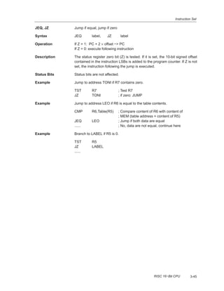
CMP[.W] Compare source and destination
CMP.B Compare source and destination
Syntax CMP src,dst or CMP.W src,dst
CMP.B src,dst
Operation dst + .NOT.src + 1
or
(dst − src)
Description The source operand is subtracted from the destination operand. This is
accomplished by adding the 1s complement of the source operand plus 1. The
two operands are not affected and the result is not stored; only the status bits
are affected.
Status Bits N: Set if result is negative, reset if positive (src >= dst)
Z: Set if result is zero, reset otherwise (src = dst)
C: Set if there is a carry from the MSB of the result, reset otherwise
V: Set if an arithmetic overflow occurs, otherwise reset
Mode Bits OSCOFF, CPUOFF, and GIE are not affected.
Example R5 and R6 are compared. If they are equal, the program continues at the label
EQUAL.
CMP R5,R6 ; R5 = R6?
JEQ EQUAL ; YES, JUMP
Example Two RAM blocks are compared. If they are not equal, the program branches
to the label ERROR.
MOV #NUM,R5 ; number of words to be compared
MOV #BLOCK1,R6 ; BLOCK1 start address in R6
MOV #BLOCK2,R7 ; BLOCK2 start address in R7
L$1 CMP @R6+,0(R7) ; Are Words equal? R6 increments
JNZ ERROR ; No, branch to ERROR
INCD R7 ; Increment R7 pointer
DEC R5 ; Are all words compared?
JNZ L$1 ; No, another compare
Example The RAM bytes addressed by EDE and TONI are compared. If they are equal,
the program continues at the label EQUAL.
CMP.B EDE,TONI ; MEM(EDE) = MEM(TONI)?
JEQ EQUAL ; YES, JUMP](https://image.slidesharecdn.com/430ugslau049f-101123080121-phpapp01/85/430ug-slau049f-68-320.jpg)
![Instruction Set
3-35RISC 16−Bit CPU
* DADC[.W] Add carry decimally to destination
* DADC.B Add carry decimally to destination
Syntax DADC dst or DADC.W src,dst
DADC.B dst
Operation dst + C −> dst (decimally)
Emulation DADD #0,dst
DADD.B #0,dst
Description The carry bit (C) is added decimally to the destination.
Status Bits N: Set if MSB is 1
Z: Set if dst is 0, reset otherwise
C: Set if destination increments from 9999 to 0000, reset otherwise
Set if destination increments from 99 to 00, reset otherwise
V: Undefined
Mode Bits OSCOFF, CPUOFF, and GIE are not affected.
Example The four-digit decimal number contained in R5 is added to an eight-digit deci-
mal number pointed to by R8.
CLRC ; Reset carry
; next instruction’s start condition is defined
DADD R5,0(R8) ; Add LSDs + C
DADC 2(R8) ; Add carry to MSD
Example The two-digit decimal number contained in R5 is added to a four-digit decimal
number pointed to by R8.
CLRC ; Reset carry
; next instruction’s start condition is defined
DADD.B R5,0(R8) ; Add LSDs + C
DADC 1(R8) ; Add carry to MSDs](https://image.slidesharecdn.com/430ugslau049f-101123080121-phpapp01/85/430ug-slau049f-69-320.jpg)
![Instruction Set
3-36 RISC 16−Bit CPU
DADD[.W] Source and carry added decimally to destination
DADD.B Source and carry added decimally to destination
Syntax DADD src,dst or DADD.W src,dst
DADD.B src,dst
Operation src + dst + C −> dst (decimally)
Description The source operand and the destination operand are treated as four binary
coded decimals (BCD) with positive signs. The source operand and the carry
bit (C) are added decimally to the destination operand. The source operand
is not affected. The previous contents of the destination are lost. The result is
not defined for non-BCD numbers.
Status Bits N: Set if the MSB is 1, reset otherwise
Z: Set if result is zero, reset otherwise
C: Set if the result is greater than 9999
Set if the result is greater than 99
V: Undefined
Mode Bits OSCOFF, CPUOFF, and GIE are not affected.
Example The eight-digit BCD number contained in R5 and R6 is added decimally to an
eight-digit BCD number contained in R3 and R4 (R6 and R4 contain the
MSDs).
CLRC ; clear carry
DADD R5,R3 ; add LSDs
DADD R6,R4 ; add MSDs with carry
JC OVERFLOW ; If carry occurs go to error handling routine
Example The two-digit decimal counter in the RAM byte CNT is incremented by one.
CLRC ; clear carry
DADD.B #1,CNT ; increment decimal counter
or
SETC
DADD.B #0,CNT ; ≡ DADC.B CNT](https://image.slidesharecdn.com/430ugslau049f-101123080121-phpapp01/85/430ug-slau049f-70-320.jpg)
![Instruction Set
3-37RISC 16−Bit CPU
* DEC[.W] Decrement destination
* DEC.B Decrement destination
Syntax DEC dst or DEC.W dst
DEC.B dst
Operation dst − 1 −> dst
Emulation SUB #1,dst
Emulation SUB.B #1,dst
Description The destination operand is decremented by one. The original contents are
lost.
Status Bits N: Set if result is negative, reset if positive
Z: Set if dst contained 1, reset otherwise
C: Reset if dst contained 0, set otherwise
V: Set if an arithmetic overflow occurs, otherwise reset.
Set if initial value of destination was 08000h, otherwise reset.
Set if initial value of destination was 080h, otherwise reset.
Mode Bits OSCOFF, CPUOFF, and GIE are not affected.
Example R10 is decremented by 1
DEC R10 ; Decrement R10
; Move a block of 255 bytes from memory location starting with EDE to memory location starting with
;TONI. Tables should not overlap: start of destination address TONI must not be within the range EDE
; to EDE+0FEh
;
MOV #EDE,R6
MOV #255,R10
L$1 MOV.B @R6+,TONI−EDE−1(R6)
DEC R10
JNZ L$1
; Do not transfer tables using the routine above with the overlap shown in Figure 3−12.
Figure 3−12. Decrement Overlap
EDE
EDE+254
TONI
TONI+254](https://image.slidesharecdn.com/430ugslau049f-101123080121-phpapp01/85/430ug-slau049f-71-320.jpg)
![Instruction Set
3-38 RISC 16−Bit CPU
* DECD[.W] Double-decrement destination
* DECD.B Double-decrement destination
Syntax DECD dst or DECD.W dst
DECD.B dst
Operation dst − 2 −> dst
Emulation SUB #2,dst
Emulation SUB.B #2,dst
Description The destination operand is decremented by two. The original contents are lost.
Status Bits N: Set if result is negative, reset if positive
Z: Set if dst contained 2, reset otherwise
C: Reset if dst contained 0 or 1, set otherwise
V: Set if an arithmetic overflow occurs, otherwise reset.
Set if initial value of destination was 08001 or 08000h, otherwise reset.
Set if initial value of destination was 081 or 080h, otherwise reset.
Mode Bits OSCOFF, CPUOFF, and GIE are not affected.
Example R10 is decremented by 2.
DECD R10 ; Decrement R10 by two
; Move a block of 255 words from memory location starting with EDE to memory location
; starting with TONI
; Tables should not overlap: start of destination address TONI must not be within the
; range EDE to EDE+0FEh
;
MOV #EDE,R6
MOV #510,R10
L$1 MOV @R6+,TONI−EDE−2(R6)
DECD R10
JNZ L$1
Example Memory at location LEO is decremented by two.
DECD.B LEO ; Decrement MEM(LEO)
Decrement status byte STATUS by two.
DECD.B STATUS](https://image.slidesharecdn.com/430ugslau049f-101123080121-phpapp01/85/430ug-slau049f-72-320.jpg)


![Instruction Set
3-41RISC 16−Bit CPU
* INC[.W] Increment destination
* INC.B Increment destination
Syntax INC dst or INC.W dst
INC.B dst
Operation dst + 1 −> dst
Emulation ADD #1,dst
Description The destination operand is incremented by one. The original contents are lost.
Status Bits N: Set if result is negative, reset if positive
Z: Set if dst contained 0FFFFh, reset otherwise
Set if dst contained 0FFh, reset otherwise
C: Set if dst contained 0FFFFh, reset otherwise
Set if dst contained 0FFh, reset otherwise
V: Set if dst contained 07FFFh, reset otherwise
Set if dst contained 07Fh, reset otherwise
Mode Bits OSCOFF, CPUOFF, and GIE are not affected.
Example The status byte, STATUS, of a process is incremented. When it is equal to 11,
a branch to OVFL is taken.
INC.B STATUS
CMP.B #11,STATUS
JEQ OVFL](https://image.slidesharecdn.com/430ugslau049f-101123080121-phpapp01/85/430ug-slau049f-75-320.jpg)
![Instruction Set
3-42 RISC 16−Bit CPU
* INCD[.W] Double-increment destination
* INCD.B Double-increment destination
Syntax INCD dst or INCD.W dst
INCD.B dst
Operation dst + 2 −> dst
Emulation ADD #2,dst
Emulation ADD.B #2,dst
Example The destination operand is incremented by two. The original contents are lost.
Status Bits N: Set if result is negative, reset if positive
Z: Set if dst contained 0FFFEh, reset otherwise
Set if dst contained 0FEh, reset otherwise
C: Set if dst contained 0FFFEh or 0FFFFh, reset otherwise
Set if dst contained 0FEh or 0FFh, reset otherwise
V: Set if dst contained 07FFEh or 07FFFh, reset otherwise
Set if dst contained 07Eh or 07Fh, reset otherwise
Mode Bits OSCOFF, CPUOFF, and GIE are not affected.
Example The item on the top of the stack (TOS) is removed without using a register.
.......
PUSH R5 ; R5 is the result of a calculation, which is stored
; in the system stack
INCD SP ; Remove TOS by double-increment from stack
; Do not use INCD.B, SP is a word-aligned
; register
RET
Example The byte on the top of the stack is incremented by two.
INCD.B 0(SP) ; Byte on TOS is increment by two](https://image.slidesharecdn.com/430ugslau049f-101123080121-phpapp01/85/430ug-slau049f-76-320.jpg)
![Instruction Set
3-43RISC 16−Bit CPU
* INV[.W] Invert destination
* INV.B Invert destination
Syntax INV dst
INV.B dst
Operation .NOT.dst −> dst
Emulation XOR #0FFFFh,dst
Emulation XOR.B #0FFh,dst
Description The destination operand is inverted. The original contents are lost.
Status Bits N: Set if result is negative, reset if positive
Z: Set if dst contained 0FFFFh, reset otherwise
Set if dst contained 0FFh, reset otherwise
C: Set if result is not zero, reset otherwise ( = .NOT. Zero)
Set if result is not zero, reset otherwise ( = .NOT. Zero)
V: Set if initial destination operand was negative, otherwise reset
Mode Bits OSCOFF, CPUOFF, and GIE are not affected.
Example Content of R5 is negated (twos complement).
MOV #00AEh,R5 ; R5 = 000AEh
INV R5 ; Invert R5, R5 = 0FF51h
INC R5 ; R5 is now negated, R5 = 0FF52h
Example Content of memory byte LEO is negated.
MOV.B #0AEh,LEO ; MEM(LEO) = 0AEh
INV.B LEO ; Invert LEO, MEM(LEO) = 051h
INC.B LEO ; MEM(LEO) is negated,MEM(LEO) = 052h](https://image.slidesharecdn.com/430ugslau049f-101123080121-phpapp01/85/430ug-slau049f-77-320.jpg)


![Instruction Set
3-52 RISC 16−Bit CPU
MOV[.W] Move source to destination
MOV.B Move source to destination
Syntax MOV src,dst or MOV.W src,dst
MOV.B src,dst
Operation src −> dst
Description The source operand is moved to the destination.
The source operand is not affected. The previous contents of the destination
are lost.
Status Bits Status bits are not affected.
Mode Bits OSCOFF, CPUOFF, and GIE are not affected.
Example The contents of table EDE (word data) are copied to table TOM. The length
of the tables must be 020h locations.
MOV #EDE,R10 ; Prepare pointer
MOV #020h,R9 ; Prepare counter
Loop MOV @R10+,TOM−EDE−2(R10) ; Use pointer in R10 for both tables
DEC R9 ; Decrement counter
JNZ Loop ; Counter ≠ 0, continue copying
...... ; Copying completed
......
......
Example The contents of table EDE (byte data) are copied to table TOM. The length of
the tables should be 020h locations
MOV #EDE,R10 ; Prepare pointer
MOV #020h,R9 ; Prepare counter
Loop MOV.B @R10+,TOM−EDE−1(R10) ; Use pointer in R10 for
; both tables
DEC R9 ; Decrement counter
JNZ Loop ; Counter ≠ 0, continue
; copying
...... ; Copying completed
......
......](https://image.slidesharecdn.com/430ugslau049f-101123080121-phpapp01/85/430ug-slau049f-86-320.jpg)

![Instruction Set
3-54 RISC 16−Bit CPU
* POP[.W] Pop word from stack to destination
* POP.B Pop byte from stack to destination
Syntax POP dst
POP.B dst
Operation @SP −> temp
SP + 2 −> SP
temp −> dst
Emulation MOV @SP+,dst or MOV.W @SP+,dst
Emulation MOV.B @SP+,dst
Description The stack location pointed to by the stack pointer (TOS) is moved to the
destination. The stack pointer is incremented by two afterwards.
Status Bits Status bits are not affected.
Example The contents of R7 and the status register are restored from the stack.
POP R7 ; Restore R7
POP SR ; Restore status register
Example The contents of RAM byte LEO is restored from the stack.
POP.B LEO ; The low byte of the stack is moved to LEO.
Example The contents of R7 is restored from the stack.
POP.B R7 ; The low byte of the stack is moved to R7,
; the high byte of R7 is 00h
Example The contents of the memory pointed to by R7 and the status register are
restored from the stack.
POP.B 0(R7) ; The low byte of the stack is moved to the
; the byte which is pointed to by R7
: Example: R7 = 203h
; Mem(R7) = low byte of system stack
: Example: R7 = 20Ah
; Mem(R7) = low byte of system stack
POP SR ; Last word on stack moved to the SR
Note: The System Stack Pointer
The system stack pointer (SP) is always incremented by two, independent
of the byte suffix.](https://image.slidesharecdn.com/430ugslau049f-101123080121-phpapp01/85/430ug-slau049f-88-320.jpg)
![Instruction Set
3-55RISC 16−Bit CPU
PUSH[.W] Push word onto stack
PUSH.B Push byte onto stack
Syntax PUSH src or PUSH.W src
PUSH.B src
Operation SP − 2 → SP
src → @SP
Description The stack pointer is decremented by two, then the source operand is moved
to the RAM word addressed by the stack pointer (TOS).
Status Bits Status bits are not affected.
Mode Bits OSCOFF, CPUOFF, and GIE are not affected.
Example The contents of the status register and R8 are saved on the stack.
PUSH SR ; save status register
PUSH R8 ; save R8
Example The contents of the peripheral TCDAT is saved on the stack.
PUSH.B &TCDAT ; save data from 8-bit peripheral module,
; address TCDAT, onto stack
Note: The System Stack Pointer
The system stack pointer (SP) is always decremented by two, independent
of the byte suffix.](https://image.slidesharecdn.com/430ugslau049f-101123080121-phpapp01/85/430ug-slau049f-89-320.jpg)


![Instruction Set
3-58 RISC 16−Bit CPU
* RLA[.W] Rotate left arithmetically
* RLA.B Rotate left arithmetically
Syntax RLA dst or RLA.W dst
RLA.B dst
Operation C <− MSB <− MSB−1 .... LSB+1 <− LSB <− 0
Emulation ADD dst,dst
ADD.B dst,dst
Description The destination operand is shifted left one position as shown in Figure 3−14.
The MSB is shifted into the carry bit (C) and the LSB is filled with 0. The RLA
instruction acts as a signed multiplication by 2.
An overflow occurs if dst ≥ 04000h and dst < 0C000h before operation is
performed: the result has changed sign.
Figure 3−14. Destination Operand—Arithmetic Shift Left
15 0
7 0
C
Byte
Word
0
An overflow occurs if dst ≥ 040h and dst < 0C0h before the operation is
performed: the result has changed sign.
Status Bits N: Set if result is negative, reset if positive
Z: Set if result is zero, reset otherwise
C: Loaded from the MSB
V: Set if an arithmetic overflow occurs:
the initial value is 04000h ≤ dst < 0C000h; reset otherwise
Set if an arithmetic overflow occurs:
the initial value is 040h ≤ dst < 0C0h; reset otherwise
Mode Bits OSCOFF, CPUOFF, and GIE are not affected.
Example R7 is multiplied by 2.
RLA R7 ; Shift left R7 (× 2)
Example The low byte of R7 is multiplied by 4.
RLA.B R7 ; Shift left low byte of R7 (× 2)
RLA.B R7 ; Shift left low byte of R7 (× 4)
Note: RLA Substitution
The assembler does not recognize the instruction:
RLA @R5+, RLA.B @R5+, or RLA(.B) @R5
It must be substituted by:
ADD @R5+,−2(R5) ADD.B @R5+,−1(R5) or ADD(.B) @R5](https://image.slidesharecdn.com/430ugslau049f-101123080121-phpapp01/85/430ug-slau049f-92-320.jpg)
![Instruction Set
3-59RISC 16−Bit CPU
* RLC[.W] Rotate left through carry
* RLC.B Rotate left through carry
Syntax RLC dst or RLC.W dst
RLC.B dst
Operation C <− MSB <− MSB−1 .... LSB+1 <− LSB <− C
Emulation ADDC dst,dst
Description The destination operand is shifted left one position as shown in Figure 3−15.
The carry bit (C) is shifted into the LSB and the MSB is shifted into the carry
bit (C).
Figure 3−15. Destination Operand—Carry Left Shift
15 0
7 0
C
Byte
Word
Status Bits N: Set if result is negative, reset if positive
Z: Set if result is zero, reset otherwise
C: Loaded from the MSB
V: Set if an arithmetic overflow occurs
the initial value is 04000h ≤ dst < 0C000h; reset otherwise
Set if an arithmetic overflow occurs:
the initial value is 040h ≤ dst < 0C0h; reset otherwise
Mode Bits OSCOFF, CPUOFF, and GIE are not affected.
Example R5 is shifted left one position.
RLC R5 ; (R5 x 2) + C −> R5
Example The input P1IN.1 information is shifted into the LSB of R5.
BIT.B #2,&P1IN ; Information −> Carry
RLC R5 ; Carry=P0in.1 −> LSB of R5
Example The MEM(LEO) content is shifted left one position.
RLC.B LEO ; Mem(LEO) x 2 + C −> Mem(LEO)
Note: RLC and RLC.B Substitution
The assembler does not recognize the instruction:
RLC @R5+, RLC.B @R5+, or RLC(.B) @R5
It must be substituted by:
ADDC @R5+,−2(R5) ADDC.B @R5+,−1(R5) or ADDC(.B) @R5](https://image.slidesharecdn.com/430ugslau049f-101123080121-phpapp01/85/430ug-slau049f-93-320.jpg)
![Instruction Set
3-60 RISC 16−Bit CPU
RRA[.W] Rotate right arithmetically
RRA.B Rotate right arithmetically
Syntax RRA dst or RRA.W dst
RRA.B dst
Operation MSB −> MSB, MSB −> MSB−1, ... LSB+1 −> LSB, LSB −> C
Description The destination operand is shifted right one position as shown in Figure 3−16.
The MSB is shifted into the MSB, the MSB is shifted into the MSB−1, and the
LSB+1 is shifted into the LSB.
Figure 3−16. Destination Operand—Arithmetic Right Shift
15 0
15 0
C
Byte
Word
Status Bits N: Set if result is negative, reset if positive
Z: Set if result is zero, reset otherwise
C: Loaded from the LSB
V: Reset
Mode Bits OSCOFF, CPUOFF, and GIE are not affected.
Example R5 is shifted right one position. The MSB retains the old value. It operates
equal to an arithmetic division by 2.
RRA R5 ; R5/2 −> R5
; The value in R5 is multiplied by 0.75 (0.5 + 0.25).
;
PUSH R5 ; Hold R5 temporarily using stack
RRA R5 ; R5 × 0.5 −> R5
ADD @SP+,R5 ; R5 × 0.5 + R5 = 1.5 × R5 −> R5
RRA R5 ; (1.5 × R5) × 0.5 = 0.75 × R5 −> R5
......
Example The low byte of R5 is shifted right one position. The MSB retains the old value.
It operates equal to an arithmetic division by 2.
RRA.B R5 ; R5/2 −> R5: operation is on low byte only
; High byte of R5 is reset
PUSH.B R5 ; R5 × 0.5 −> TOS
RRA.B @SP ; TOS × 0.5 = 0.5 × R5 × 0.5 = 0.25 × R5 −> TOS
ADD.B @SP+,R5 ; R5 × 0.5 + R5 × 0.25 = 0.75 × R5 −> R5
......](https://image.slidesharecdn.com/430ugslau049f-101123080121-phpapp01/85/430ug-slau049f-94-320.jpg)
![Instruction Set
3-61RISC 16−Bit CPU
RRC[.W] Rotate right through carry
RRC.B Rotate right through carry
Syntax RRC dst or RRC.W dst
RRC dst
Operation C −> MSB −> MSB−1 .... LSB+1 −> LSB −> C
Description The destination operand is shifted right one position as shown in Figure 3−17.
The carry bit (C) is shifted into the MSB, the LSB is shifted into the carry bit (C).
Figure 3−17. Destination Operand—Carry Right Shift
15 0
7 0
C
Byte
Word
Status Bits N: Set if result is negative, reset if positive
Z: Set if result is zero, reset otherwise
C: Loaded from the LSB
V: Reset
Mode Bits OSCOFF, CPUOFF, and GIE are not affected.
Example R5 is shifted right one position. The MSB is loaded with 1.
SETC ; Prepare carry for MSB
RRC R5 ; R5/2 + 8000h −> R5
Example R5 is shifted right one position. The MSB is loaded with 1.
SETC ; Prepare carry for MSB
RRC.B R5 ; R5/2 + 80h −> R5; low byte of R5 is used](https://image.slidesharecdn.com/430ugslau049f-101123080121-phpapp01/85/430ug-slau049f-95-320.jpg)
![Instruction Set
3-62 RISC 16−Bit CPU
* SBC[.W] Subtract source and borrow/.NOT. carry from destination
* SBC.B Subtract source and borrow/.NOT. carry from destination
Syntax SBC dst or SBC.W dst
SBC.B dst
Operation dst + 0FFFFh + C −> dst
dst + 0FFh + C −> dst
Emulation SUBC #0,dst
SUBC.B #0,dst
Description The carry bit (C) is added to the destination operand minus one. The previous
contents of the destination are lost.
Status Bits N: Set if result is negative, reset if positive
Z: Set if result is zero, reset otherwise
C: Set if there is a carry from the MSB of the result, reset otherwise.
Set to 1 if no borrow, reset if borrow.
V: Set if an arithmetic overflow occurs, reset otherwise.
Mode Bits OSCOFF, CPUOFF, and GIE are not affected.
Example The 16-bit counter pointed to by R13 is subtracted from a 32-bit counter
pointed to by R12.
SUB @R13,0(R12) ; Subtract LSDs
SBC 2(R12) ; Subtract carry from MSD
Example The 8-bit counter pointed to by R13 is subtracted from a 16-bit counter pointed
to by R12.
SUB.B @R13,0(R12) ; Subtract LSDs
SBC.B 1(R12) ; Subtract carry from MSD
Note: Borrow Implementation.
The borrow is treated as a .NOT. carry : Borrow Carry bit
Yes 0
No 1](https://image.slidesharecdn.com/430ugslau049f-101123080121-phpapp01/85/430ug-slau049f-96-320.jpg)


![Instruction Set
3-66 RISC 16−Bit CPU
SUB[.W] Subtract source from destination
SUB.B Subtract source from destination
Syntax SUB src,dst or SUB.W src,dst
SUB.B src,dst
Operation dst + .NOT.src + 1 −> dst
or
[(dst − src −> dst)]
Description The source operand is subtracted from the destination operand by adding the
source operand’s 1s complement and the constant 1. The source operand is
not affected. The previous contents of the destination are lost.
Status Bits N: Set if result is negative, reset if positive
Z: Set if result is zero, reset otherwise
C: Set if there is a carry from the MSB of the result, reset otherwise.
Set to 1 if no borrow, reset if borrow.
V: Set if an arithmetic overflow occurs, otherwise reset
Mode Bits OSCOFF, CPUOFF, and GIE are not affected.
Example See example at the SBC instruction.
Example See example at the SBC.B instruction.
Note: Borrow Is Treated as a .NOT.
The borrow is treated as a .NOT. carry : Borrow Carry bit
Yes 0
No 1](https://image.slidesharecdn.com/430ugslau049f-101123080121-phpapp01/85/430ug-slau049f-100-320.jpg)
![Instruction Set
3-67RISC 16−Bit CPU
SUBC[.W]SBB[.W] Subtract source and borrow/.NOT. carry from destination
SUBC.B,SBB.B Subtract source and borrow/.NOT. carry from destination
Syntax SUBC src,dst or SUBC.W src,dst or
SBB src,dst or SBB.W src,dst
SUBC.B src,dst or SBB.B src,dst
Operation dst + .NOT.src + C −> dst
or
(dst − src − 1 + C −> dst)
Description The source operand is subtracted from the destination operand by adding the
source operand’s 1s complement and the carry bit (C). The source operand
is not affected. The previous contents of the destination are lost.
Status Bits N: Set if result is negative, reset if positive.
Z: Set if result is zero, reset otherwise.
C: Set if there is a carry from the MSB of the result, reset otherwise.
Set to 1 if no borrow, reset if borrow.
V: Set if an arithmetic overflow occurs, reset otherwise.
Mode Bits OSCOFF, CPUOFF, and GIE are not affected.
Example Two floating point mantissas (24 bits) are subtracted.
LSBs are in R13 and R10, MSBs are in R12 and R9.
SUB.W R13,R10 ; 16-bit part, LSBs
SUBC.B R12,R9 ; 8-bit part, MSBs
Example The 16-bit counter pointed to by R13 is subtracted from a 16-bit counter in R10
and R11(MSD).
SUB.B @R13+,R10 ; Subtract LSDs without carry
SUBC.B @R13,R11 ; Subtract MSDs with carry
... ; resulting from the LSDs
Note: Borrow Implementation
The borrow is treated as a .NOT. carry : Borrow Carry bit
Yes 0
No 1](https://image.slidesharecdn.com/430ugslau049f-101123080121-phpapp01/85/430ug-slau049f-101-320.jpg)


![Instruction Set
3-70 RISC 16−Bit CPU
* TST[.W] Test destination
* TST.B Test destination
Syntax TST dst or TST.W dst
TST.B dst
Operation dst + 0FFFFh + 1
dst + 0FFh + 1
Emulation CMP #0,dst
CMP.B #0,dst
Description The destination operand is compared with zero. The status bits are set accord-
ing to the result. The destination is not affected.
Status Bits N: Set if destination is negative, reset if positive
Z: Set if destination contains zero, reset otherwise
C: Set
V: Reset
Mode Bits OSCOFF, CPUOFF, and GIE are not affected.
Example R7 is tested. If it is negative, continue at R7NEG; if it is positive but not zero,
continue at R7POS.
TST R7 ; Test R7
JN R7NEG ; R7 is negative
JZ R7ZERO ; R7 is zero
R7POS ...... ; R7 is positive but not zero
R7NEG ...... ; R7 is negative
R7ZERO ...... ; R7 is zero
Example The low byte of R7 is tested. If it is negative, continue at R7NEG; if it is positive
but not zero, continue at R7POS.
TST.B R7 ; Test low byte of R7
JN R7NEG ; Low byte of R7 is negative
JZ R7ZERO ; Low byte of R7 is zero
R7POS ...... ; Low byte of R7 is positive but not zero
R7NEG ..... ; Low byte of R7 is negative
R7ZERO ...... ; Low byte of R7 is zero](https://image.slidesharecdn.com/430ugslau049f-101123080121-phpapp01/85/430ug-slau049f-104-320.jpg)
![Instruction Set
3-71RISC 16−Bit CPU
XOR[.W] Exclusive OR of source with destination
XOR.B Exclusive OR of source with destination
Syntax XOR src,dst or XOR.W src,dst
XOR.B src,dst
Operation src .XOR. dst −> dst
Description The source and destination operands are exclusive ORed. The result is placed
into the destination. The source operand is not affected.
Status Bits N: Set if result MSB is set, reset if not set
Z: Set if result is zero, reset otherwise
C: Set if result is not zero, reset otherwise ( = .NOT. Zero)
V: Set if both operands are negative
Mode Bits OSCOFF, CPUOFF, and GIE are not affected.
Example The bits set in R6 toggle the bits in the RAM word TONI.
XOR R6,TONI ; Toggle bits of word TONI on the bits set in R6
Example The bits set in R6 toggle the bits in the RAM byte TONI.
XOR.B R6,TONI ; Toggle bits of byte TONI on the bits set in
; low byte of R6
Example Reset to 0 those bits in low byte of R7 that are different from bits in RAM byte
EDE.
XOR.B EDE,R7 ; Set different bit to “1s”
INV.B R7 ; Invert Lowbyte, Highbyte is 0h](https://image.slidesharecdn.com/430ugslau049f-101123080121-phpapp01/85/430ug-slau049f-105-320.jpg)


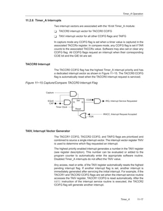
![DMA Operation
8-7DMA Controller
Figure 8−3.DMA Single Transfer State Diagram
Reset
Wait for Trigger
Idle
Hold CPU,
Transfer one word/byte
[+Trigger AND DMALEVEL = 0 ]
OR
[Trigger=1 AND DMALEVEL=1]
DMAABORT=0
DMAABORT = 1
2 x MCLK
DMAEN = 0
Modify T_SourceAdd
Modify T_DestAdd
Decrement DMAxSZ
[ENNMI = 1
AND NMI event]
OR
[DMALEVEL = 1
AND Trigger = 0]
[ DMADTx = 0
AND DMAxSZ = 0]
OR DMAEN = 0
DMAxSZ → T_Size
DMAxSA → T_SourceAdd
DMAxDA → T_DestAdd
DMAREQ = 0
DMAxSZ > 0
AND DMAEN = 1
DMAEN = 0
DMAEN = 1
T_Size → DMAxSZ
DMAxSA → T_SourceAdd
DMAxDA → T_DestAdd
DMADTx = 4
AND DMAxSZ = 0
AND DMAEN = 1
DMAEN = 0
DMAREQ = 0
T_Size → DMAxSZ](https://image.slidesharecdn.com/430ugslau049f-101123080121-phpapp01/85/430ug-slau049f-168-320.jpg)

![DMA Operation
8-9DMA Controller
Figure 8−4.DMA Block Transfer State Diagram
Reset
Wait for Trigger
Idle
Hold CPU,
Transfer one word/byte
[+Trigger AND DMALEVEL = 0 ]
OR
[Trigger=1 AND DMALEVEL=1]
DMAABORT=0
DMAABORT = 1
2 x MCLK
DMAEN = 0
Modify T_SourceAdd
Modify T_DestAdd
Decrement DMAxSZ
DMAxSZ > 0
[ENNMI = 1
AND NMI event]
OR
[DMALEVEL = 1
AND Trigger = 0]
[DMADTx = 1
AND DMAxSZ = 0]
OR
DMAEN = 0
DMAxSZ → T_Size
DMAxSA → T_SourceAdd
DMAxDA → T_DestAdd
DMAREQ = 0
T_Size → DMAxSZ
DMAxSA → T_SourceAdd
DMAxDA → T_DestAdd
DMADTx = 5
AND DMAxSZ = 0
AND DMAEN = 1
DMAEN = 0
DMAEN = 1
DMAEN = 0
DMAREQ = 0
T_Size → DMAxSZ](https://image.slidesharecdn.com/430ugslau049f-101123080121-phpapp01/85/430ug-slau049f-170-320.jpg)

![DMA Operation
8-11DMA Controller
Figure 8−5.DMA Burst-Block Transfer State Diagram
2 x MCLK
Reset
Wait for Trigger
Idle
Hold CPU,
Transfer one word/byte
Burst State
(release CPU for 2xMCLK)
[+Trigger AND DMALEVEL = 0 ]
OR
[Trigger=1 AND DMALEVEL=1]
DMAABORT=0
DMAABORT = 1
2 x MCLK
DMAEN = 0
Modify T_SourceAdd
Modify T_DestAdd
Decrement DMAxSZ
[DMADTx = {6, 7}
AND DMAxSZ = 0]
[ENNMI = 1
AND NMI event]
OR
[DMALEVEL = 1
AND Trigger = 0]
[DMADTx = {2, 3}
AND DMAxSZ = 0]
OR
DMAEN = 0
DMAxSZ → T_Size
DMAxSA → T_SourceAdd
DMAxDA → T_DestAdd
T_Size → DMAxSZ
DMAxSA → T_SourceAdd
DMAxDA → T_DestAdd
DMAEN = 0
DMAEN = 1
DMAxSZ > 0
DMAxSZ > 0 AND
a multiple of 4 words/bytes
were transferred
DMAxSZ > 0
DMAEN = 0
DMAREQ = 0
T_Size → DMAxSZ](https://image.slidesharecdn.com/430ugslau049f-101123080121-phpapp01/85/430ug-slau049f-172-320.jpg)


![USART Operation: UART Mode
13-4 USART Peripheral Interface, UART Mode
13.2 USART Operation: UART Mode
In UART mode, the USART transmits and receives characters at a bit rate
asynchronous to another device. Timing for each character is based on the
selected baud rate of the USART. The transmit and receive functions use the
same baud rate frequency.
13.2.1 USART Initialization and Reset
The USART is reset by a PUC or by setting the SWRST bit. After a PUC, the
SWRST bit is automatically set, keeping the USART in a reset condition. When
set, the SWRST bit resets the URXIEx, UTXIEx, URXIFGx, RXWAKE,
TXWAKE, RXERR, BRK, PE, OE, and FE bits and sets the UTXIFGx and
TXEPT bits. The receive and transmit enable flags, URXEx and UTXEx, are
not altered by SWRST. Clearing SWRST releases the USART for operation.
See also chapter USART Module, I2C mode for USART0 when reconfiguring
from I2C mode to UART mode.
Note: Initializing or Re-Configuring the USART Module
The required USART initialization/re-configuration process is:
1) Set SWRST (BIS.B #SWRST,&UxCTL)
2) Initialize all USART registers with SWRST = 1 (including UxCTL)
3) Enable USART module via the MEx SFRs (URXEx and/or UTXEx)
4) Clear SWRST via software (BIC.B #SWRST,&UxCTL)
5) Enable interrupts (optional) via the IEx SFRs (URXIEx and/or UTXIEx)
Failure to follow this process may result in unpredictable USART behavior.
13.2.2 Character Format
The UART character format, shown in Figure 13−2, consists of a start bit,
seven or eight data bits, an even/odd/no parity bit, an address bit (address-bit
mode), and one or two stop bits. The bit period is defined by the selected clock
source and setup of the baud rate registers.
Figure 13−2. Character Format
[Parity Bit, PENA = 1]
[Address Bit, MM = 1]
Mark
Space
D0 D6 D7 AD PA SP SP
[Optional Bit, Condition]
[2nd Stop Bit, SP = 1]
[8th Data Bit, CHAR = 1]
ST](https://image.slidesharecdn.com/430ugslau049f-101123080121-phpapp01/85/430ug-slau049f-253-320.jpg)


![USART Operation: UART Mode
13-13USART Peripheral Interface, UART Mode
Transmit Bit Timing
The timing for each character is the sum of the individual bit timings. By
modulating each bit, the cumulative bit error is reduced. The individual bit error
can be calculated by:
Error [%] + NJbaud rate
BRCLK
ƪ(j ) 1) UxBR ) S
j
i+0
miƫ* (j ) 1)Nj 100%
With:
baud rate: Desired baud rate
BRCLK: Input frequency − UCLKI, ACLK, or SMCLK
j: Bit position - 0 for the start bit, 1 for data bit D0, and so on
UxBR: Division factor in registers UxBR1 and UxBR0
For example, the transmit errors for the following conditions are calculated:
Baud rate = 2400
BRCLK = 32,768 Hz (ACLK)
UxBR = 13, since the ideal division factor is 13.65
UxMCTL = 6Bh: m7=0, m6=1, m5=1, m4=0, m3=1, m2=0,
m1=1, and m0=1. The LSB of UxMCTL is used first.
Start bit Error [%] + ǒbaud rate
BRCLK
((0 ) 1) UxBR ) 1)–1Ǔ 100% + 2.54%
Data bit D0 Error [%] + ǒbaud rate
BRCLK
((1 ) 1) UxBR ) 2)–2Ǔ 100% + 5.08%
Data bit D1 Error [%] + ǒbaud rate
BRCLK
((2 ) 1) UxBR ) 2)–3Ǔ 100% + 0.29%
Data bit D2 Error [%] + ǒbaud rate
BRCLK
((3 ) 1) UxBR ) 3)–4Ǔ 100% + 2.83%
Data bit D3 Error [%] + ǒbaud rate
BRCLK
((4 ) 1) UxBR ) 3)–5Ǔ 100% +*1.95%
Data bit D4 Error [%] + ǒbaud rate
BRCLK
((5 ) 1) UxBR ) 4)–6Ǔ 100% + 0.59%
Data bit D5 Error [%] + ǒbaud rate
BRCLK
((6 ) 1) UxBR ) 5)–7Ǔ 100% + 3.13%
Data bit D6 Error [%] + ǒbaud rate
BRCLK
((7 ) 1) UxBR ) 5)–8Ǔ 100% + *1.66%
Data bit D7 Error [%] + ǒbaud rate
BRCLK
((8 ) 1) UxBR ) 6)–9Ǔ 100% + 0.88%
Parity bit Error [%] + ǒbaud rate
BRCLK
((9 ) 1) UxBR ) 7)–10Ǔ 100% + 3.42%
Stop bit 1 Error [%] + ǒbaud rate
BRCLK
((10 ) 1) UxBR ) 7)–11Ǔ 100% + *1.37%
The results show the maximum per-bit error to be 5.08% of a BITCLK period.](https://image.slidesharecdn.com/430ugslau049f-101123080121-phpapp01/85/430ug-slau049f-262-320.jpg)
![USART Operation: UART Mode
13-14 USART Peripheral Interface, UART Mode
Receive Bit Timing
Receive timing consists of two error sources. The first is the bit-to-bit timing
error. The second is the error between a start edge occurring and the start
edge being accepted by the USART. Figure 13−9 shows the asynchronous
timing errors between data on the URXDx pin and the internal baud-rate clock.
Figure 13−9. Receive Error
1 2 3 4 5 6
0i
t0tideal
7 8
1
t1
2
9 10 11 12 13 14 1 2 3 4 5 6 7 8 9 10 11 12 13 14 1 2 3 4 5 6 7
t0 t1 t2
ST D0 D1
D0 D1ST
Synchronization Error ± 0.5x BRCLK
Int(UxBR/2)+m0 =
Int (13/2)+1 = 6+1 = 7
Majority Vote Taken Majority Vote Taken
UxBR +m1 = 13+1 = 14 UxBR +m2 = 13+0 = 13
Majority Vote Taken
BRCLK
URXDx
URXDS
tactual
Sample
URXDS
The ideal start bit timing tideal(0) is half the baud-rate timing tbaud rate because
the bit is tested in the middle of its period. The ideal baud rate timing tideal(i) for
the remaining character bits is the baud rate timing tbaud rate. The individual bit
errors can be calculated by:
Error [%] +ȧ
ȡ
Ȣ
baud rate
BRCLK
NJ2 ƪm0 ) int ǒUxBR
2
Ǔƫ) ǒi UxBR ) S
j
i+1
mi ǓNj* 1 * jǓ 100%
Where:
baud rate is the required baud rate
BRCLK is the input frequency—selected for UCLK, ACLK, or SMCLK
j = 0 for the start bit, 1 for data bit D0, and so on
UxBR is the division factor in registers UxBR1 and UxBR0](https://image.slidesharecdn.com/430ugslau049f-101123080121-phpapp01/85/430ug-slau049f-263-320.jpg)
![USART Operation: UART Mode
13-15USART Peripheral Interface, UART Mode
For example, the receive errors for the following conditions are calculated:
Baud rate = 2400
BRCLK = 32,768 Hz (ACLK)
UxBR = 13, since the ideal division factor is 13.65
UxMCTL = 6B:m7=0, m6=1, m5=1, m4=0, m3=1, m2=0, m1=1 and
m0=1 The LSB of UxMCTL is used first.
Data bit D1 Error [%] + ǒbaud rate
BRCLK
[2x(1 ) 6) ) (2 UxBR ) 1)]–1–2Ǔ 100% + 0.29%
Data bit D2 Error [%] + ǒbaud rate
BRCLK
[2x(1 ) 6) ) (3 UxBR ) 2)]–1–3Ǔ 100% + 2.83%
Data bit D3 Error [%] + ǒbaud rate
BRCLK
[2x(1 ) 6) ) (4 UxBR ) 2)]–1–4Ǔ 100% + –1.95%
Data bit D4 Error [%] + ǒbaud rate
BRCLK
[2x(1 ) 6) ) (5 UxBR ) 3)]–1–5Ǔ 100% + 0.59%
Data bit D5 Error [%] + ǒbaud rate
BRCLK
[2x(1 ) 6) ) (6 UxBR ) 4)]–1–6Ǔ 100% + 3.13%
Data bit D6 Error [%] + ǒbaud rate
BRCLK
[2x(1 ) 6) ) (7 UxBR ) 4)]–1–7Ǔ 100% + –1.66%
Data bit D7 Error [%] + ǒbaud rate
BRCLK
[2x(1 ) 6) ) (8 UxBR ) 5)]–1–8Ǔ 100% + 0.88%
Parity bit Error [%] + ǒbaud rate
BRCLK
[2x(1 ) 6) ) (9 UxBR ) 6)]–1–9Ǔ 100% + 3.42%
Stop bit 1 Error [%] + ǒbaud rate
BRCLK
[2x(1 ) 6) ) (10 UxBR ) 6)]–1–10Ǔ 100% + –1.37%
Start bit Error [%] + ǒbaud rate
BRCLK
[2x(1 ) 6) ) (0 UxBR ) 0)] * 1 * 0Ǔ 100% + 2.54%
Data bit D0 Error [%] + ǒbaud rate
BRCLK
[2x(1 ) 6) ) (1 UxBR ) 1)]–1–1Ǔ 100% + 5.08%
The results show the maximum per-bit error to be 5.08% of a BITCLK period.](https://image.slidesharecdn.com/430ugslau049f-101123080121-phpapp01/85/430ug-slau049f-264-320.jpg)


![USART Operation: SPI Mode
14-9USART Peripheral Interface, SPI Mode
14.2.5 Serial Clock Control
UCLK is provided by the master on the SPI bus. When MM = 1, BITCLK is
provided by the USART baud rate generator on the UCLK pin as shown in
Figure 14−8. When MM = 0, the USART clock is provided on the UCLK pin by
the master and, the baud rate generator is not used and the SSELx bits are
don’t care. The SPI receiver and transmitter operate in parallel and use the
same clock source for data transfer.
Figure 14−8. SPI Baud Rate Generator
Bit Start
mX
BRCLK
88UCLKI
ACLK
SMCLK
SMCLK 11
BITCLK
10
01
00
202728215
Compare (0 or 1)
Modulation Data Shift Register
(LSB first)
16−Bit Counter
Q0............Q15
m0m7
......
8
UxBR1 UxBR0
Toggle
FF
N =
R
R
R
UxMCTL
SSEL1 SSEL0
The 16-bit value of UxBR0+UxBR1 is the division factor of the USART clock
source, BRCLK. The maximum baud rate that can be generated in master
mode is BRCLK/2. The maximum baud rate that can be generated in slave
mode is BRCLK. The modulator in the USART baud rate generator is not used
for SPI mode and is recommended to be set to 000h. The UCLK frequency is
given by:
Baud rate = BRCLK
UxBR
with UxBR= [UxBR1, UxBR0]](https://image.slidesharecdn.com/430ugslau049f-101123080121-phpapp01/85/430ug-slau049f-288-320.jpg)