Download to read offline
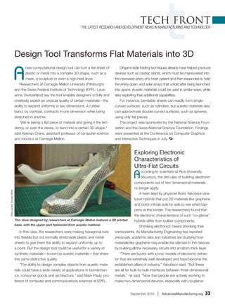


1) Researchers at Carnegie Mellon University and EPFL have developed a new computational design tool that can transform flat sheets of materials like plastic or metal into complex 3D shapes by introducing hexagonal cuts that allow for uniform expansion. 2) Scientists at Rice University have found that the traditional models of electronic behavior do not apply to ultra-flat 2D material interfaces and have simulated novel electric field effects at the boundaries of 2D materials like graphene. 3) Researchers at Georgia Tech have created the most efficient humanoid robot to date, called Durus, which walks with a natural human gait involving heel strikes and toe-off, achieving higher efficiency than flat-footed robots.


