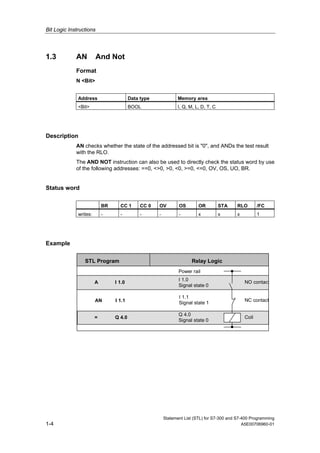
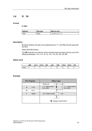
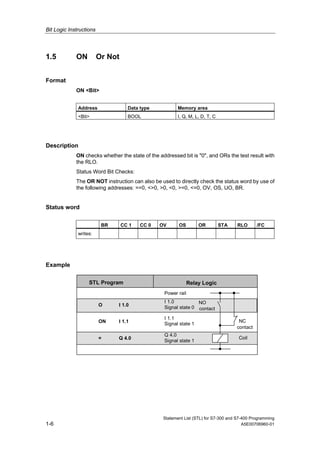
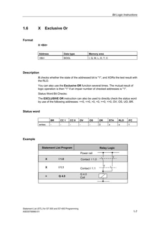
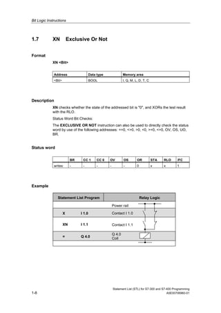
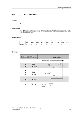
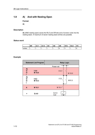
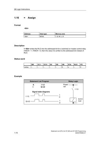
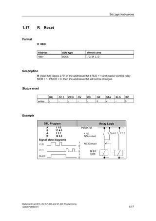
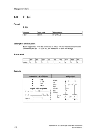
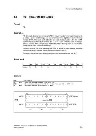
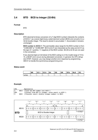
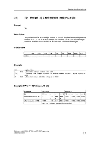
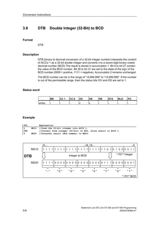
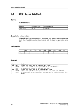
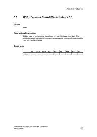
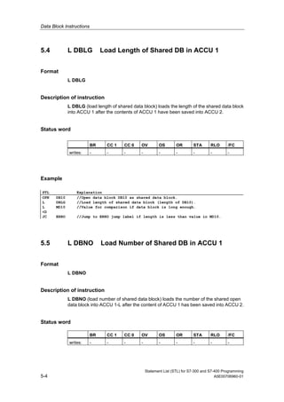
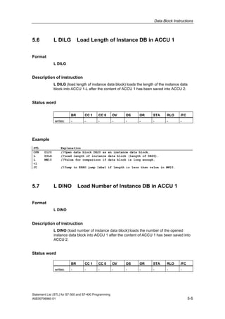
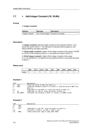
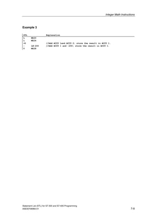
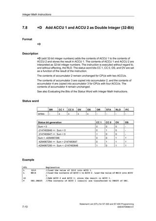
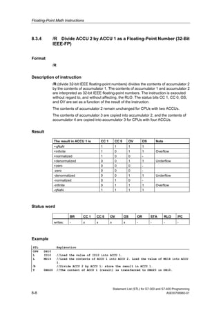
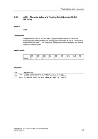
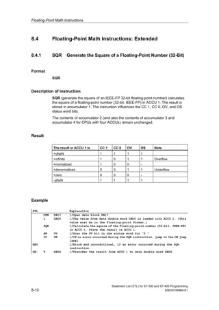
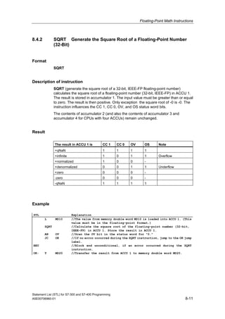
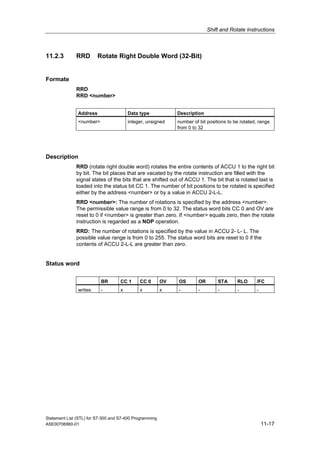
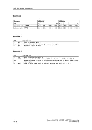
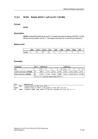
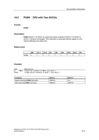
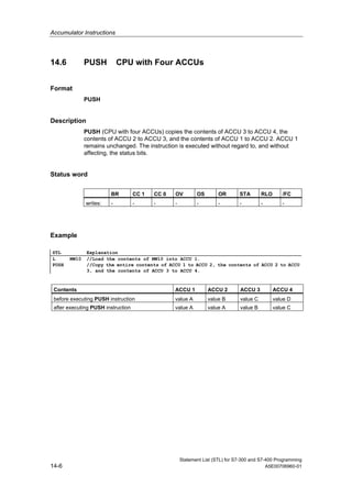
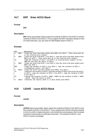
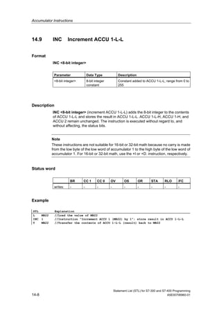
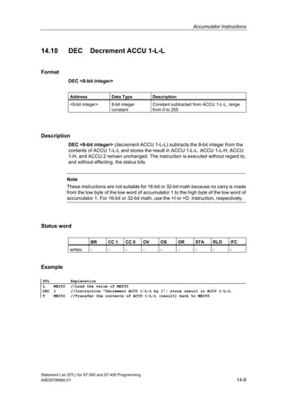
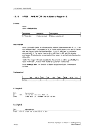
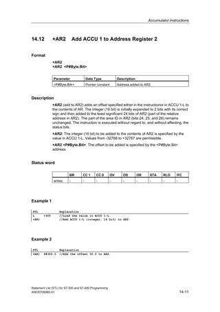
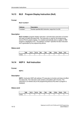
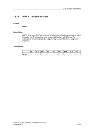
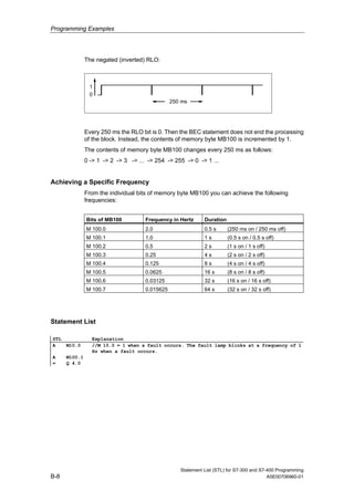
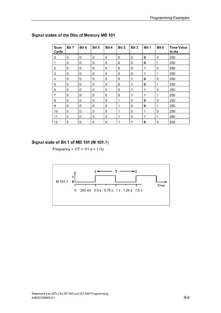
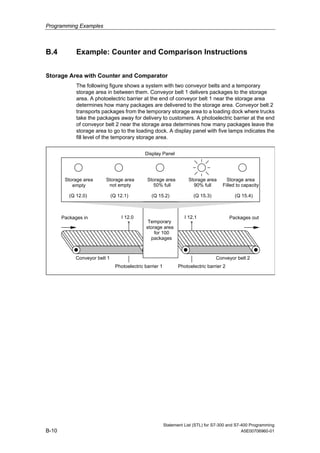
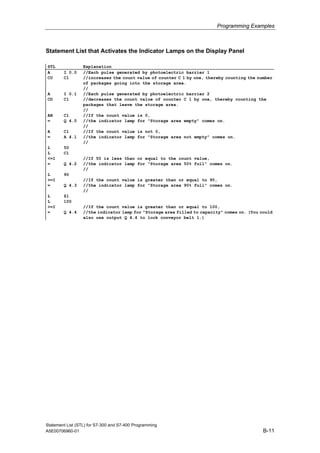
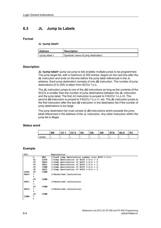
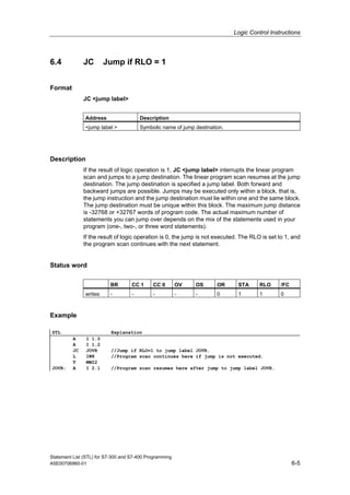
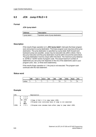
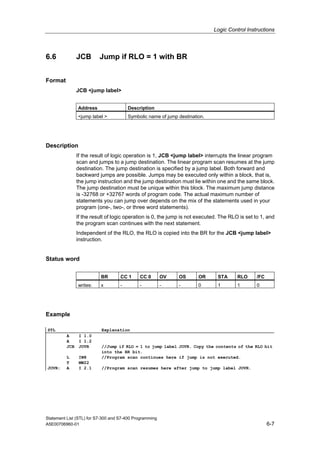
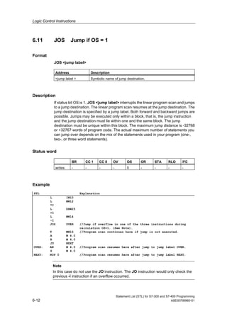
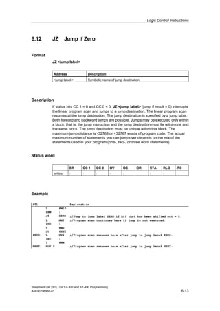
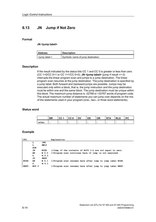
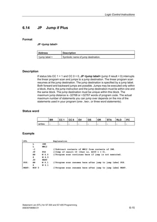
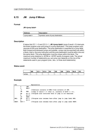
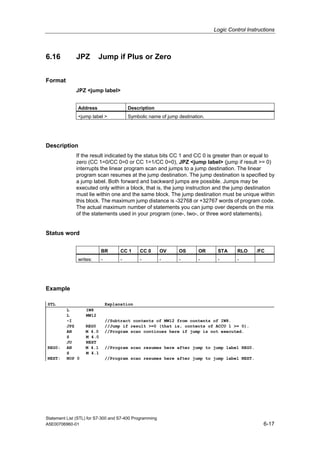
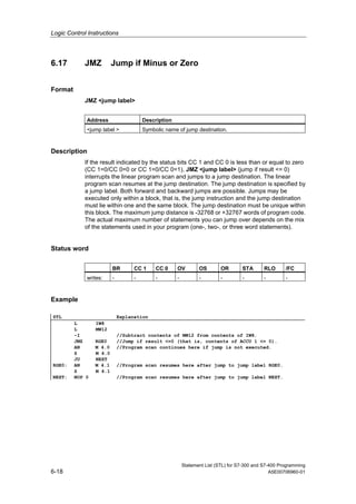
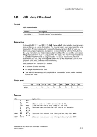
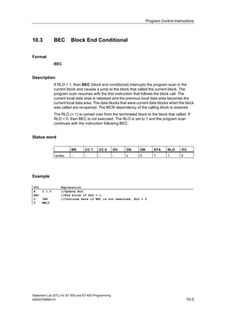
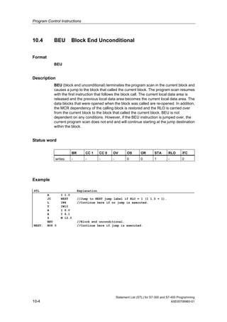
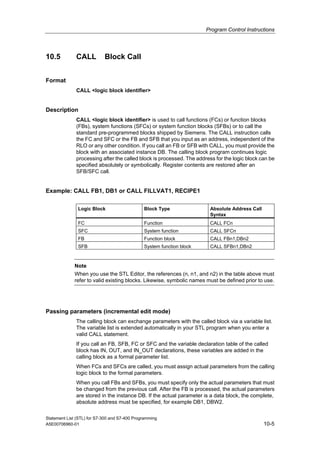
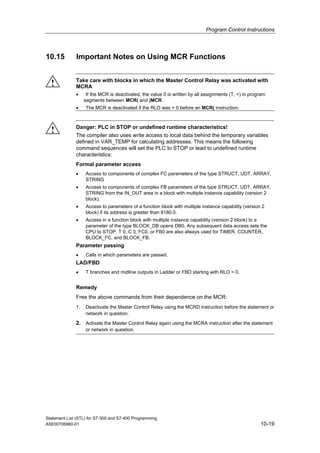
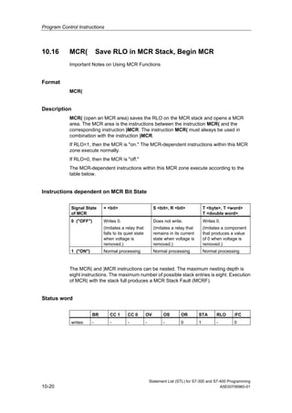
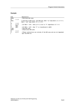
s
Preface,
Contents
Bit Logic Instructions 1
Comparison Instructions 2
Conversion Instructions 3
Counter Instructions 4
Data Block Instructions 5
Logic Control Instructions 6
Integer Math Instructions 7
Floating-Point Math
Instructions 8
Load and Transfer Instructions 9
Program Control Instructions 10
Shift and Rotate Instructions 11
Timer Instructions 12
Word Logic Instructions 13
Accumulator Instructions 14
Appendices
Overview of All STL
Instructions A
Programming Examples B
SIMATIC
Statement List (STL) for
S7-300 and S7-400
Programming
Reference Manual
This manual is part of the documentation
package with the order number:
6ES7810-4CA08-8BW1
Parameter Transfer C
Edition 03/2003
A5E00706960-01
Index
Siemens AG
Automation and Drives
Postfach 4848
90437 NÜRNBERG
GERMANY
A5E00706960-01
03/2006
Copyright © Siemens AG 2006
Technical data subject to change
Safety Guidelines
This manual contains notices you have to observe in order to ensure your personal safety, as well as to
prevent damage to property. The notices referring to your personal safety are highlighted in the manual
by a safety alert symbol, notices referring to property damage only have no safety alert symbol. The
notices shown below are graded according to the degree of danger.
! Danger
indicates that death or severe personal injury will result if proper precautions are not taken.
! Warning
indicates that death or severe personal injury may result if proper precautions are not taken.
! Caution
with a safety alert symbol indicates that minor personal injury can result if proper precautions are not
taken.
Caution
without a safety alert symbol indicates that property damage can result if proper precautions are not
taken.
Notice
indicates that an unintended result or situation can occur if the corresponding notice is not taken into
account.
If more than one degree of danger is present, the warning notice representing the highest degree of
danger will be used. A notice warning of injury to persons with a safety alert symbol may also include a
warning relating to property damage.
Qualified Personnel
The device/system may only be set up and used in conjunction with this documentation. Commissioning
and operation of a device/system may only be performed by qualified personnel. Within the context of
the safety notices in this documentation qualified persons are defined as persons who are authorized to
commission, ground and label devices, systems and circuits in accordance with established safety
practices and standards.
Prescribed Usage
Note the following:
!
Warning
This device and its components may only be used for the applications described in the catalog or the
technical description, and only in connection with devices or components from other manufacturers
which have been approved or recommended by Siemens.
Correct, reliable operation of the product requires proper transport, storage, positioning and assembly
as well as careful operation and maintenance.
Trademarks
All names identified by ® are registered trademarks of the Siemens AG.
The remaining trademarks in this publication may be trademarks whose use by third parties for their
own purposes could violate the rights of the owner.
Disclaimer of Liability
We have reviewed the contents of this publication to ensure consistency with the hardware and
software described. Since variance cannot be precluded entirely, we cannot guarantee full consistency.
However, the information in this publication is reviewed regularly and any necessary corrections are
included in subsequent editions.
Statement List (STL) for S7-300 and S7-400 Programming
A5E00706960-01 iii
Preface
Purpose
This manual is your guide to creating user programs in the Statement List
programming language STL.
The manual also includes a reference section that describes the syntax and
functions of the language elements of STL.
Basic Knowledge Required
The manual is intended for S7 programmers, operators, and maintenance/service
personnel.
In order to understand this manual, general knowledge of automation technology is
required.
In addition to, computer literacy and the knowledge of other working equipment
similar to the PC (e.g. programming devices) under the operating systems
MS Windows 2000 Professional, XP Professional or MS Windows Server 2003 are
required.
Scope of the Manual
This manual is valid for release 5.4 of the STEP 7 programming software package.
Compliance with Standards
STL corresponds to the "Instruction List" language defined in the International
Electrotechnical Commission's standard IEC 1131-3, although there are substantial
differences with regard to the operations. For further details, refer to the table of
standards in the STEP 7 file NORM_TBL.WRI.
Preface
Statement List (STL) for S7-300 and S7-400 Programming
iv A5E00706960-01
Requirements
To use the Statement List manual effectively, you should already be familiar with
the theory behind S7 programs which is documented in the online help for STEP 7.
The language packages also use the STEP 7 standard software, so you should be
familiar with handling this software and have read the accompanying
documentation.
This manual is part of the documentation package "STEP 7 Reference".
The following table displays an overview of the STEP 7 documentation:
Documentation Purpose Order Number
STEP 7 Basic Information with
• Working with STEP 7,
Getting Started Manual
• Programming with STEP 7
• Configuring Hardware and
Communication Connections,
STEP 7
• From S5 to S7, Converter Manual
Basic information for technical
personnel describing the methods
of implementing control tasks with
STEP 7 and the S7-300/400
programmable controllers.
6ES7810-4CA08-8BW0
STEP 7 Reference with
• Ladder Logic (LAD)/Function Block
Diagram (FBD)/Statement List (STL) for
S7-300/400 manuals
• Standard and System Functions
for S7-300/400
Volume 1 and Volume 2
Provides reference information
and describes the programming
languages LAD, FBD, and STL,
and standard and system
functions extending the scope of
the STEP 7 basic information.
6ES7810-4CA08-8BW1
Online Helps Purpose Order Number
Help on STEP 7 Basic information on
programming and configuring
hardware with STEP 7 in the form
of an online help.
Part of the STEP 7
Standard software.
Reference helps on STL/LAD/FBD
Reference help on SFBs/SFCs
Reference help on Organization Blocks
Context-sensitive reference
information.
Part of the STEP 7
Standard software.
Preface
Statement List (STL) for S7-300 and S7-400 Programming
A5E00706960-01 v
Online Help
The manual is complemented by an online help which is integrated in the software.
This online help is intended to provide you with detailed support when using the
software.
The help system is integrated in the software via a number of interfaces:
• The context-sensitive help offers information on the current context, for
example, an open dialog box or an active window. You can open the context-
sensitive help via the menu command Help > Context-Sensitive Help, by
pressing F1 or by using the question mark symbol in the toolbar.
• You can call the general Help on STEP 7 using the menu command Help >
Contents or the "Help on STEP 7" button in the context-sensitive help window.
• You can call the glossary for all STEP 7 applications via the "Glossary" button.
This manual is an extract from the "Help on Statement List". As the manual and the
online help share an identical structure, it is easy to switch between the manual
and the online help.
Further Support
If you have any technical questions, please get in touch with your Siemens
representative or responsible agent.
You will find your contact person at:
http://www.siemens.com/automation/partner
You will find a guide to the technical documentation offered for the individual
SIMATIC Products and Systems here at:
http://www.siemens.com/simatic-tech-doku-portal
The online catalog and order system is found under:
http://mall.automation.siemens.com/
Training Centers
Siemens offers a number of training courses to familiarize you with the SIMATIC
S7 automation system. Please contact your regional training center or our central
training center in D 90327 Nuremberg, Germany for details:
Telephone: +49 (911) 895-3200.
Internet: http://www.sitrain.com
Preface
Statement List (STL) for S7-300 and S7-400 Programming
vi A5E00706960-01
Technical Support
You can reach the Technical Support for all A&D products
• Via the Web formula for the Support Request
http://www.siemens.com/automation/support-request
• Phone: + 49 180 5050 222
• Fax: + 49 180 5050 223
Additional information about our Technical Support can be found on the Internet
pages http://www.siemens.com/automation/service
Service & Support on the Internet
In addition to our documentation, we offer our Know-how online on the internet at:
http://www.siemens.com/automation/service&support
where you will find the following:
• The newsletter, which constantly provides you with up-to-date information on
your products.
• The right documents via our Search function in Service & Support.
• A forum, where users and experts from all over the world exchange their
experiences.
• Your local representative for Automation & Drives.
• Information on field service, repairs, spare parts and more under "Services".
Statement List (STL) for S7-300 and S7-400 Programming
A5E00706960-01 vii
Contents
1 Bit Logic Instructions 1-1
1.1 Overview of Bit Logic Instructions .................................................................... 1-1
1.2 A And ............................................................................................................. 1-3
1.3 AN And Not.................................................................................................... 1-4
1.4 O Or ............................................................................................................... 1-5
1.5 ON Or Not...................................................................................................... 1-6
1.6 X Exclusive Or ............................................................................................... 1-7
1.7 XN Exclusive Or Not...................................................................................... 1-8
1.8 O And before Or ............................................................................................ 1-9
1.9 A( And with Nesting Open ........................................................................... 1-10
1.10 AN( And Not with Nesting Open.................................................................. 1-11
1.11 O( Or with Nesting Open ............................................................................. 1-11
1.12 ON( Or Not with Nesting Open.................................................................... 1-12
1.13 X( Exclusive Or with Nesting Open ............................................................. 1-12
1.14 XN( Exclusive Or Not with Nesting Open .................................................... 1-13
1.15 ) Nesting Closed .......................................................................................... 1-14
1.16 = Assign....................................................................................................... 1-16
1.17 R Reset........................................................................................................ 1-17
1.18 S Set ............................................................................................................ 1-18
1.19 NOT Negate RLO ........................................................................................ 1-19
1.20 SET Set RLO (=1) ....................................................................................... 1-20
1.21 CLR Clear RLO (=0).................................................................................... 1-21
1.22 SAVE Save RLO in BR Register ................................................................. 1-22
1.23 FN Edge Negative ....................................................................................... 1-23
1.24 FP Edge Positive ......................................................................................... 1-25
2 Comparison Instructions 2-1
2.1 Overview of Comparison Instructions............................................................... 2-1
2.2 ? I Compare Integer (16-Bit)............................................................................ 2-2
2.3 ? D Compare Double Integer (32-Bit).............................................................. 2-3
2.4 ? R Compare Floating-Point Number (32-Bit) ................................................. 2-4
3 Conversion Instructions 3-1
3.1 Overview of Conversion Instructions................................................................ 3-1
3.2 BTI BCD to Integer (16-Bit) ........................................................................... 3-2
3.3 ITB Integer (16-Bit) to BCD ........................................................................... 3-3
3.4 BTD BCD to Integer (32-Bit).......................................................................... 3-4
3.5 ITD Integer (16 Bit) to Double Integer (32-Bit) .............................................. 3-5
3.6 DTB Double Integer (32-Bit) to BCD ............................................................. 3-6
3.7 DTR Double Integer (32-Bit) to Floating-Point (32-Bit IEEE-FP) ................... 3-7
3.8 INVI Ones Complement Integer (16-Bit)........................................................ 3-8
3.9 INVD Ones Complement Double Integer (32-Bit) ......................................... 3-9
3.10 NEGI Twos Complement Integer (16-Bit).................................................... 3-10
3.11 NEGD Twos Complement Double Integer (32-Bit)...................................... 3-11
3.12 NEGR Negate Floating-Point Number (32-Bit, IEEE-FP)............................ 3-12
3.13 CAW Change Byte Sequence in ACCU 1-L (16-Bit)................................... 3-13
3.14 CAD Change Byte Sequence in ACCU 1 (32-Bit)....................................... 3-14
3.15 RND Round ................................................................................................. 3-15
Contents
Statement List (STL) for S7-300 and S7-400 Programming
viii A5E00706960-01
3.16 TRUNC Truncate......................................................................................... 3-16
3.17 RND+ Round to Upper Double Integer........................................................ 3-17
3.18 RND- Round to Lower Double Integer......................................................... 3-18
4 Counter Instructions 4-1
4.1 Overview of Counter Instructions ..................................................................... 4-1
4.2 FR Enable Counter (Free) ............................................................................. 4-2
4.3 L Load Current Counter Value into ACCU 1 ................................................. 4-3
4.4 LC Load Current Counter Value into ACCU 1 as BCD ................................. 4-4
4.5 R Reset Counter............................................................................................ 4-5
4.6 S Set Counter Preset Value .......................................................................... 4-6
4.7 CU Counter Up .............................................................................................. 4-7
4.8 CD Counter Down.......................................................................................... 4-8
5 Data Block Instructions 5-1
5.1 Overview of Data Block Instructions................................................................. 5-1
5.2 OPN Open a Data Block................................................................................ 5-2
5.3 CDB Exchange Shared DB and Instance DB................................................ 5-3
5.4 L DBLG Load Length of Shared DB in ACCU 1............................................ 5-4
5.5 L DBNO Load Number of Shared DB in ACCU 1.......................................... 5-4
5.6 L DILG Load Length of Instance DB in ACCU 1 ........................................... 5-5
5.7 L DINO Load Number of Instance DB in ACCU 1......................................... 5-5
6 Logic Control Instructions 6-1
6.1 Overview of Logic Control Instructions............................................................. 6-1
6.2 JU Jump Unconditional.................................................................................. 6-3
6.3 JL Jump to Labels.......................................................................................... 6-4
6.4 JC Jump if RLO = 1 ....................................................................................... 6-5
6.5 JCN Jump if RLO = 0..................................................................................... 6-6
6.6 JCB Jump if RLO = 1 with BR ....................................................................... 6-7
6.7 JNB Jump if RLO = 0 with BR ....................................................................... 6-8
6.8 JBI Jump if BR = 1......................................................................................... 6-9
6.9 JNBI Jump if BR = 0 .................................................................................... 6-10
6.10 JO Jump if OV = 1 ....................................................................................... 6-11
6.11 JOS Jump if OS = 1..................................................................................... 6-12
6.12 JZ Jump if Zero............................................................................................ 6-13
6.13 JN Jump if Not Zero..................................................................................... 6-14
6.14 JP Jump if Plus............................................................................................ 6-15
6.15 JM Jump if Minus......................................................................................... 6-16
6.16 JPZ Jump if Plus or Zero ............................................................................. 6-17
6.17 JMZ Jump if Minus or Zero.......................................................................... 6-18
6.18 JUO Jump if Unordered............................................................................... 6-19
6.19 LOOP Loop.................................................................................................. 6-20
7 Integer Math Instructions 7-1
7.1 Overview of Integer Math Instructions.............................................................. 7-1
7.2 Evaluating the Bits of the Status Word with Integer Math Instructions............. 7-2
7.3 +I Add ACCU 1 and ACCU 2 as Integer (16-Bit)........................................... 7-3
7.4 -I Subtract ACCU 1 from ACCU 2 as Integer (16-Bit) ................................... 7-4
7.5 *I Multiply ACCU 1 and ACCU 2 as Integer (16-Bit)...................................... 7-5
7.6 /I Divide ACCU 2 by ACCU 1 as Integer (16-Bit) .......................................... 7-6
7.7 + Add Integer Constant (16, 32-Bit)............................................................... 7-8
7.8 +D Add ACCU 1 and ACCU 2 as Double Integer (32-Bit)........................... 7-10
7.9 -D Subtract ACCU 1 from ACCU 2 as Double Integer (32-Bit) ................... 7-11
7.10 *D Multiply ACCU 1 and ACCU 2 as Double Integer (32-Bit)...................... 7-12
7.11 /D Divide ACCU 2 by ACCU 1 as Double Integer (32-Bit) .......................... 7-13
7.12 MOD Division Remainder Double Integer (32-Bit) ...................................... 7-15
Contents
Statement List (STL) for S7-300 and S7-400 Programming
A5E00706960-01 ix
8 Floating-Point Math Instructions 8-1
8.1 Overview of Floating-Point Math Instructions................................................... 8-1
8.2 Evaluating the Bits of the Status Word with Floating-Point Math Instructions.. 8-2
8.3 Floating-Point Math Instructions: Basic ............................................................ 8-3
8.3.1 +R Add ACCU 1 and ACCU 2 as a Floating-Point Number
(32-Bit IEEE-FP)...............................................................................................8-3
8.3.2 -R Subtract ACCU 1 from ACCU 2 as a Floating-Point Number
(32-Bit IEEE-FP)...............................................................................................8-5
8.3.3 *R Multiply ACCU 1 and ACCU 2 as Floating-Point Numbers
(32-Bit IEEE-FP)...............................................................................................8-7
8.3.4 /R Divide ACCU 2 by ACCU 1 as a Floating-Point Number
(32-Bit IEEE-FP)...............................................................................................8-8
8.3.5 ABS Absolute Value of a Floating-Point Number (32-Bit IEEE-FP)..............8-9
8.4 Floating-Point Math Instructions: Extended.................................................... 8-10
8.4.1 SQR Generate the Square of a Floating-Point Number (32-Bit).................8-10
8.4.2 SQRT Generate the Square Root of a Floating-Point Number (32-Bit) ......8-11
8.4.3 EXP Generate the Exponential Value of a Floating-Point Number (32-Bit) 8-12
8.4.4 LN Generate the Natural Logarithm of a Floating-Point Number (32-Bit) ...8-13
8.4.5 SIN Generate the Sine of Angles as Floating-Point Numbers (32-Bit)........8-14
8.4.6 COS Generate the Cosine of Angles as Floating-Point Numbers (32-Bit)..8-15
8.4.7 TAN Generate the Tangent of Angles as Floating-Point Numbers (32-Bit) 8-16
8.4.8 ASIN Generate the Arc Sine of a Floating-Point Number (32-Bit) ..............8-17
8.4.9 ACOS Generate the Arc Cosine of a Floating-Point Number (32-Bit).........8-18
8.4.10 ATAN Generate the Arc Tangent of a Floating-Point Number (32-Bit) .......8-19
9 Load and Transfer Instructions 9-1
9.1 Overview of Load and Transfer Instructions..................................................... 9-1
9.2 L Load............................................................................................................ 9-2
9.3 L STW Load Status Word into ACCU 1......................................................... 9-4
9.4 LAR1 Load Address Register 1 from ACCU 1 .............................................. 9-5
9.5 LAR1 <D> Load Address Register 1 with Double Integer (32-Bit Pointer).... 9-6
9.6 LAR1 AR2 Load Address Register 1 from Address Register 2..................... 9-7
9.7 LAR2 Load Address Register 2 from ACCU 1 .............................................. 9-7
9.8 LAR2 <D> Load Address Register 2 with Double Integer (32-Bit Pointer).... 9-8
9.9 T Transfer ...................................................................................................... 9-9
9.10 T STW Transfer ACCU 1 into Status Word ................................................. 9-10
9.11 CAR Exchange Address Register 1 with Address Register 2 ..................... 9-11
9.12 TAR1 Transfer Address Register 1 to ACCU 1 ........................................... 9-11
9.13 TAR1 <D> Transfer Address Register 1 to Destination (32-Bit Pointer)..... 9-12
9.14 TAR1 AR2 Transfer Address Register 1 to Address Register 2 ................. 9-13
9.15 TAR2 Transfer Address Register 2 to ACCU 1 ........................................... 9-13
9.16 TAR2 <D> Transfer Address Register 2 to Destination (32-Bit Pointer)..... 9-14
10 Program Control Instructions 10-1
10.1 Overview of Program Control Instructions...................................................... 10-1
10.2 BE Block End............................................................................................... 10-2
10.3 BEC Block End Conditional......................................................................... 10-3
10.4 BEU Block End Unconditional ..................................................................... 10-4
10.5 CALL Block Call........................................................................................... 10-5
10.6 Call FB ............................................................................................................ 10-7
10.7 Call FC............................................................................................................ 10-9
10.8 Call SFB........................................................................................................ 10-11
10.9 Call SFC ....................................................................................................... 10-13
Contents
Statement List (STL) for S7-300 and S7-400 Programming
x A5E00706960-01
10.10 Call Multiple Instance.................................................................................... 10-14
10.11 Call Block from a Library............................................................................... 10-14
10.12 CC Conditional Call ................................................................................... 10-15
10.13 UC Unconditional Call................................................................................ 10-16
10.14 MCR (Master Control Relay) ........................................................................ 10-17
10.15 Important Notes on Using MCR Functions................................................... 10-19
10.16 MCR( Save RLO in MCR Stack, Begin MCR ............................................ 10-20
10.17 )MCR End MCR......................................................................................... 10-22
10.18 MCRA Activate MCR Area ........................................................................ 10-23
10.19 MCRD Deactivate MCR Area.................................................................... 10-24
11 Shift and Rotate Instructions 11-1
11.1 Shift Instructions ............................................................................................. 11-1
11.1.1 Overview of Shift Instructions .........................................................................11-1
11.1.2 SSI Shift Sign Integer (16-Bit) .....................................................................11-2
11.1.3 SSD Shift Sign Double Integer (32-Bit) .......................................................11-4
11.1.4 SLW Shift Left Word (16-Bit) .......................................................................11-6
11.1.5 SRW Shift Right Word (16-Bit) ....................................................................11-8
11.1.6 SLD Shift Left Double Word (32-Bit)..........................................................11-10
11.1.7 SRD Shift Right Double Word (32-Bit).......................................................11-12
11.2 Rotate Instructions........................................................................................ 11-14
11.2.1 Overview of Rotate Instructions....................................................................11-14
11.2.2 RLD Rotate Left Double Word (32-Bit)......................................................11-15
11.2.3 RRD Rotate Right Double Word (32-Bit)...................................................11-17
11.2.4 RLDA Rotate ACCU 1 Left via CC 1 (32-Bit) ............................................11-19
11.2.5 RRDA Rotate ACCU 1 Right via CC 1 (32-Bit) .........................................11-20
12 Timer Instructions 12-1
12.1 Overview of Timer Instructions....................................................................... 12-1
12.2 Location of a Timer in Memory and Components of a Timer ......................... 12-2
12.3 FR Enable Timer (Free)............................................................................... 12-5
12.4 L Load Current Timer Value into ACCU 1 as Integer.................................. 12-7
12.5 LC Load Current Timer Value into ACCU 1 as BCD................................... 12-9
12.6 R Reset Timer............................................................................................ 12-11
12.7 SP Pulse Timer.......................................................................................... 12-12
12.8 SE Extended Pulse Timer ......................................................................... 12-14
12.9 SD On-Delay Timer ................................................................................... 12-16
12.10 SS Retentive On-Delay Timer ................................................................... 12-18
12.11 SF Off-Delay Timer.................................................................................... 12-20
13 Word Logic Instructions 13-1
13.1 Overview of Word Logic Instructions.............................................................. 13-1
13.2 AW AND Word (16-Bit)................................................................................ 13-2
13.3 OW OR Word (16-Bit).................................................................................. 13-4
13.4 XOW Exclusive OR Word (16-Bit)............................................................... 13-6
13.5 AD AND Double Word (32-Bit) .................................................................... 13-8
13.6 OD OR Double Word (32-Bit).................................................................... 13-10
13.7 XOD Exclusive OR Double Word (32-Bit) ................................................. 13-12
Contents
Statement List (STL) for S7-300 and S7-400 Programming
A5E00706960-01 xi
14 Accumulator Instructions 14-1
14.1 Overview of Accumulator and Address Register Instructions ........................ 14-1
14.2 TAK Toggle ACCU 1 with ACCU 2.............................................................. 14-2
14.3 POP CPU with Two ACCUs ........................................................................ 14-3
14.4 POP CPU with Four ACCUs........................................................................ 14-4
14.5 PUSH CPU with Two ACCUs...................................................................... 14-5
14.6 PUSH CPU with Four ACCUs ..................................................................... 14-6
14.7 ENT Enter ACCU Stack............................................................................... 14-7
14.8 LEAVE Leave ACCU Stack......................................................................... 14-7
14.9 INC Increment ACCU 1-L-L......................................................................... 14-8
14.10 DEC Decrement ACCU 1-L-L...................................................................... 14-9
14.11 +AR1 Add ACCU 1 to Address Register 1 ................................................ 14-10
14.12 +AR2 Add ACCU 1 to Address Register 2 ................................................ 14-11
14.13 BLD Program Display Instruction (Null)..................................................... 14-12
14.14 NOP 0 Null Instruction ............................................................................... 14-12
14.15 NOP 1 Null Instruction ............................................................................... 14-13
A Overview of All STL Instructions A-1
A.1 STL Instructions Sorted According to German Mnemonics (SIMATIC) ...........A-1
A.2 STL Instructions Sorted According to English Mnemonics (International) .......A-7
B Programming Examples B-1
B.1 Overview of Programming Examples ...............................................................B-1
B.2 Example: Bit Logic Instructions ........................................................................B-2
B.3 Example: Timer Instructions .............................................................................B-7
B.4 Example: Counter and Comparison Instructions............................................B-10
B.5 Example: Integer Math Instructions................................................................B-12
B.6 Example: Word Logic Instructions..................................................................B-13
C Parameter Transfer C-1
Index Index-1
Contents
Statement List (STL) for S7-300 and S7-400 Programming
xii A5E00706960-01
Statement List (STL) for S7-300 and S7-400 Programming
A5E00706960-01 1-1
1 Bit Logic Instructions
1.1 Overview of Bit Logic Instructions
Description
Bit logic instructions work with two digits, 1 and 0. These two digits form the base of
a number system called the binary system. The two digits 1 and 0 are called binary
digits or bits. In the world of contacts and coils, a 1 indicates activated or energized,
and a 0 indicates not activated or not energized.
The bit logic instructions interpret signal states of 1 and 0 and combine them
according to Boolean logic. These combinations produce a result of 1 or 0 that is
called the ”result of logic operation” (RLO).
Boolean bit logic applies to the following basic instructions:
• A And
• AN And Not
• O Or
• ON Or Not
• X Exclusive Or
• XN Exclusive Or Not
• O And before Or
You can use the following instructions to perform nesting expressions:
• A( And with Nesting Open
• AN( And Not with Nesting Open
• O( Or with Nesting Open
• ON( Or Not with Nesting Open
• X( Exclusive Or with Nesting Open
• XN( Exclusive Or Not with Nesting Open
• ) Nesting Closed
Bit Logic Instructions
Statement List (STL) for S7-300 and S7-400 Programming
1-2 A5E00706960-01
You can terminate a Boolean bit logic string by using one of the following
instructions:
• = Assign
• R Reset
• S Set
You can use one of the following instructions to change the result of logic operation
(RLO):
• NOT Negate RLO
• SET Set RLO (=1)
• CLR Clear RLO (=0)
• SAVE Save RLO in BR Register
Other instructions react to a positive or negative edge transition:
• FN Edge Negative
• FP Edge Positive
Bit Logic Instructions
Statement List (STL) for S7-300 and S7-400 Programming
A5E00706960-01 1-3
1.2 A And
Format
A <Bit>
Address Data type Memory area
<Bit> BOOL I, Q, M, L, D, T, C
Description
A checks whether the state of the addressed bit is "1", and ANDs the test result with
the RLO.
Status Word Bit Checks:
The AND instruction can also be used to directly check the status word by use of the
following addresses: ==0, <>0, >0, <0, >=0, <=0, OV, OS, UO, BR.
Status word
BR CC 1 CC 0 OV OS OR STA RLO /FC
writes: - - - - - x x x 1
Example
Relay LogicSTL Program
A I 1.0
A I 1.1
= Q 4.0
Power rail
I 1.0 signal state 1
I 1.1 signal state 1
Q 4.0 signal state 1
Displays closed switch
NO contact
NC contact
Coil
Bit Logic Instructions
Statement List (STL) for S7-300 and S7-400 Programming
1-4 A5E00706960-01
1.3 AN And Not
Format
N <Bit>
Address Data type Memory area
<Bit> BOOL I, Q, M, L, D, T, C
Description
AN checks whether the state of the addressed bit is "0", and ANDs the test result
with the RLO.
The AND NOT instruction can also be used to directly check the status word by use
of the following addresses: ==0, <>0, >0, <0, >=0, <=0, OV, OS, UO, BR.
Status word
BR CC 1 CC 0 OV OS OR STA RLO /FC
writes: - - - - - x x x 1
Example
STL Program
A I 1.0
AN I 1.1
= Q 4.0
Relay Logic
Power rail
I 1.0
Signal state 0
NO contact
I 1.1
Signal state 1
NC contact
Q 4.0
Signal state 0
Coil
Bit Logic Instructions
Statement List (STL) for S7-300 and S7-400 Programming
A5E00706960-01 1-5
1.4 O Or
Format
O <Bit>
Address Data type Memory area
<Bit> BOOL I, Q, M, L, D, T, C
Description
O checks whether the state of the addressed bit is "1", and ORs the test result with
the RLO.
Status Word Bit Checks:
The OR instruction can also be used to directly check the status word by use of the
following addresses: ==0, <>0, >0, <0, >=0, <=0, OV, OS, UO, BR.
Status word
BR CC 1 CC 0 OV OS OR STA RLO /FC
writes: - - - - - 0 x x 1
Example
STL Program
O I 1.0
O I 1.1
= Q 4.0
Relay Logic
Power rail
I 1.0 Signal state 1
No contact
I 1.1 Signal state 0
No contact
Q 4.0 Signal state 1 Coil
Displays closed switch
Bit Logic Instructions
Statement List (STL) for S7-300 and S7-400 Programming
1-6 A5E00706960-01
1.5 ON Or Not
Format
ON <Bit>
Address Data type Memory area
<Bit> BOOL I, Q, M, L, D, T, C
Description
ON checks whether the state of the addressed bit is "0", and ORs the test result with
the RLO.
Status Word Bit Checks:
The OR NOT instruction can also be used to directly check the status word by use of
the following addresses: ==0, <>0, >0, <0, >=0, <=0, OV, OS, UO, BR.
Status word
BR CC 1 CC 0 OV OS OR STA RLO /FC
writes:
Example
STL Program Relay Logic
Power rail
I 1.0
Signal state 0
NO
contact
Q 4.0
Signal state 1
I 1.1
Signal state 1
NC
O I 1.0
ON I 1.1
= Q 4.0 Coil
contact
Bit Logic Instructions
Statement List (STL) for S7-300 and S7-400 Programming
A5E00706960-01 1-7
1.6 X Exclusive Or
Format
X <Bit>
Address Data type Memory area
<Bit> BOOL I, Q, M, L, D, T, C
Description
X checks whether the state of the addressed bit is "1", and XORs the test result with
the RLO.
You can also use the Exclusive OR function several times. The mutual result of
logic operation is then "1" if an impair number of checked addresses is "1".
Status Word Bit Checks:
The EXCLUSIVE OR instruction can also be used to directly check the status word
by use of the following addresses: ==0, <>0, >0, <0, >=0, <=0, OV, OS, UO, BR.
Status word
BR CC 1 CC 0 OV OS OR STA RLO /FC
writes: - - - - - 0 x x 1
Example
Statement List Program
X I 1.0
X I 1.1
= Q 4.0
Power rail
Contact I 1.0
Contact I 1.1
Q 4.0
Coil
Relay Logic
Bit Logic Instructions
Statement List (STL) for S7-300 and S7-400 Programming
1-8 A5E00706960-01
1.7 XN Exclusive Or Not
Format
XN <Bit>
Address Data type Memory area
<Bit> BOOL I, Q, M, L, D, T, C
Description
XN checks whether the state of the addressed bit is "0", and XORs the test result
with the RLO.
Status Word Bit Checks:
The EXCLUSIVE OR NOT instruction can also be used to directly check the status
word by use of the following addresses: ==0, <>0, >0, <0, >=0, <=0, OV, OS, UO,
BR.
Status word
BR CC 1 CC 0 OV OS OR STA RLO /FC
writes: - - - - - 0 x x 1
Example
Statement List Program
X I 1.0
XN I 1.1
= Q 4.0
Power rail
Contact I 1.0
Contact I 1.1
Q 4.0
Coil
Relay Logic
Bit Logic Instructions
Statement List (STL) for S7-300 and S7-400 Programming
A5E00706960-01 1-9
1.8 O And before Or
Format
O
Description
The O function performs a logical OR instruction on AND functions according to the
rule: AND before OR.
Status word
BR CC 1 CC 0 OV OS OR STA RLO /FC
writes: - - - - - x 1 - x
Example
Statement List Program
Power rail
I 0.0
Q 4.0
Coil
M 10.0
M 10.1
M 0.3
I 0.2
A I 0.0
A M 10.0
= Q 4.0
A I 0.2
A M 0.3
O M 10.1
O
Relay Logic
Bit Logic Instructions
Statement List (STL) for S7-300 and S7-400 Programming
1-10 A5E00706960-01
1.9 A( And with Nesting Open
Format
A(
Description
A( (AND nesting open) saves the RLO and OR bits and a function code into the
nesting stack. A maximum of seven nesting stack entries are possible.
Status word
BR CC 1 CC 0 OV OS OR STA RLO /FC
writes: - - - - - 0 1 - 0
Example
Statement List Program
A(
O I 0.0
O M 10.0
)
= Q 4.0
Power rail
I 0.0
Q 4.0
Coil
I 0.2
A M 10.1 M 10.1
M 10.0
M10.3
A(
O I 0.2
O M 10.3
)
Relay Logic
Bit Logic Instructions
Statement List (STL) for S7-300 and S7-400 Programming
A5E00706960-01 1-11
1.10 AN( And Not with Nesting Open
Format
AN(
Description
AN( (AND NOT nesting open) saves the RLO and OR bits and a function code into
the nesting stack. A maximum of seven nesting stack entries are possible.
Status word
BR CC 1 CC 0 OV OS OR STA RLO /FC
writes: - - - - - 0 1 - 0
1.11 O( Or with Nesting Open
Format
O(
Description
O( (OR nesting open) saves the RLO and OR bits and a function code into the
nesting stack. A maximum of seven nesting stack entries are possible.
Status word
BR CC 1 CC 0 OV OS OR STA RLO /FC
writes: - - - - - 0 1 - 0
Bit Logic Instructions
Statement List (STL) for S7-300 and S7-400 Programming
1-12 A5E00706960-01
1.12 ON( Or Not with Nesting Open
Format
ON(
Description
ON( (OR NOT nesting open) saves the RLO and OR bits and a function code into the
nesting stack. A maximum of seven nesting stack entries is possible.
Status word
BR CC 1 CC 0 OV OS OR STA RLO /FC
writes: - - - - - 0 1 - 0
1.13 X( Exclusive Or with Nesting Open
Format
X(
Description
X( (XOR nesting open) saves the RLO and OR bits and a function code into the
nesting stack. A maximum of seven nesting stack entries is possible.
Status word
BR CC 1 CC 0 OV OS OR STA RLO /FC
writes: - - - - - 0 1 - 0
Bit Logic Instructions
Statement List (STL) for S7-300 and S7-400 Programming
A5E00706960-01 1-13
1.14 XN( Exclusive Or Not with Nesting Open
Format
XN(
Description
XN( (XOR NOT nesting open) saves the RLO and OR bits and a function code into
the nesting stack. A maximum of seven nesting stack entries is possible.
Status word
BR CC 1 CC 0 OV OS OR STA RLO /FC
writes: - - - - - 0 1 - 0
Bit Logic Instructions
Statement List (STL) for S7-300 and S7-400 Programming
1-14 A5E00706960-01
1.15 ) Nesting Closed
Format
)
Description
) (nesting closed) removes an entry from the nesting stack, restores the OR bit,
interconnects the RLO that is contained in the stack entry with the current RLO
according to the function code, and assigns the result to the RLO. The OR bit is also
included if the function code is "AND" or "AND NOT".
Statements which open parentheses groups:
• U( And with Nesting Open
• UN( And Not with Nesting Open
• O( Or with Nesting Open
• ON( Or Not with Nesting Open
• X( Exclusive Or with Nesting Open
• XN( Exclusive Or Not with Nesting Open
Status word
BR CC 1 CC 0 OV OS OR STA RLO /FC
writes: - - - - - x 1 x 1
Bit Logic Instructions
Statement List (STL) for S7-300 and S7-400 Programming
A5E00706960-01 1-15
Example
Statement List Program
A(
O I 0.0
O M 10.0
)
= Q 4.0
Relay Logic
Power rail
I 0.0
Q 4.0
Coil
I 0.2
A M 10.1 M 10.1
M 10.0
M10.3
A(
O I 0.2
O M 10.3
)
Bit Logic Instructions
Statement List (STL) for S7-300 and S7-400 Programming
1-16 A5E00706960-01
1.16 = Assign
Format
<Bit>
Address Data type Memory area
<Bit> BOOL I, Q, M, L, D
Description
= <Bit> writes the RLO into the addressed bit for a switched on master control relay
if MCR = 1. If MCR = 0, then the value 0 is written to the addressed bit instead of
RLO.
Status word
BR CC 1 CC 0 OV OS OR STA RLO /FC
writes: - - - - - 0 x - 0
Example
A I 1.0
= Q 4.0
I 1.0
Q 4.0
0
1
0
1
Signal state diagrams
Power
rail
Q 4.0
Coil
I 1.0
Statement List Program Relay Logic
Bit Logic Instructions
Statement List (STL) for S7-300 and S7-400 Programming
A5E00706960-01 1-17
1.17 R Reset
Format
R <Bit>
Address Data type Memory area
<Bit> BOOL I, Q, M, L, D
Description
R (reset bit) places a "0" in the addressed bit if RLO = 1 and master control relay
MCR = 1. If MCR = 0, then the addressed bit will not be changed.
Status word
BR CC 1 CC 0 OV OS OR STA RLO /FC
writes: - - - - - 0 x - 0
Example
Relay Logic
Power rail
I 1.0
NO contact
Q 4.0
Coils
Q 4.0
STL Program
A I 1.0
S Q 4.0
A I 1.1
R Q 4.0
I 1.0
I 1.1
Q 4.0
0
1
0
1
0
1
Signal state diagrams
I 1.1
NC Contact
Bit Logic Instructions
Statement List (STL) for S7-300 and S7-400 Programming
1-18 A5E00706960-01
1.18 S Set
Format
S <Bit>
Address Data type Memory area
<Bit> BOOL I, Q, M, L, D
Description of instruction
S (set bit) places a "1" in the addressed bit if RLO = 1 and the switched on master
control relay MCR = 1. If MCR = 0, the addressed bit does not change.
Status word
BR CC 1 CC 0 OV OS OR STA RLO /FC
writes: - - - - - 0 x - 0
Example
Power
rail
I 1.0
NO
contact
Q 4.0
Coil
Q 4.0
I 1.0
I 1.1
Q 4.0
0
1
0
1
0
1
Signal state diagrams
Coil
I 1.1
NC
contact
A I 1.0
S Q 4.0
A I 1.1
R Q4.0
Statement List Program Relay Logic
Bit Logic Instructions
Statement List (STL) for S7-300 and S7-400 Programming
A5E00706960-01 1-19
1.19 NOT Negate RLO
Format
NOT
Description
NOT negates the RLO.
Status word
BR CC 1 CC 0 OV OS OR STA RLO /FC
writes: - - - - - - 1 x -
Bit Logic Instructions
Statement List (STL) for S7-300 and S7-400 Programming
1-20 A5E00706960-01
1.20 SET Set RLO (=1)
Format
SET
Description
SET sets the RLO to signal state "1".
Status word
BR CC 1 CC 0 OV OS OR STA RLO /FC
writes: - - - - - 0 1 1 0
Example
STL Program Signal State Result of Logic Operation (RLO)
SET
= M 10.0
= M 15.1
= M 16.0
CLR
= M 10.1
= M 10.2
1
0
1
1
1
0
0
Bit Logic Instructions
Statement List (STL) for S7-300 and S7-400 Programming
A5E00706960-01 1-21
1.21 CLR Clear RLO (=0)
Format
CLR
Description
CLR sets the RLO to signal state "0".
Status word
BR CC 1 CC 0 OV OS OR STA RLO /FC
writes: - - - - - 0 0 0 0
Example
Statement List Signal State Result of Logic Operation (RLO)
SET
= M 10.0
= M 15.1
= M 16.0
CLR
= M 10.1
= M 10.2
1
0
1
1
1
0
0
Bit Logic Instructions
Statement List (STL) for S7-300 and S7-400 Programming
1-22 A5E00706960-01
1.22 SAVE Save RLO in BR Register
Format
SAVE
Description of instruction
SAVE saves the RLO into the BR bit. The first check bit /FC is not reset. For this
reason, the status of the BR bit is included in the AND logic operation in the next
network.
The use of SAVE and a subsequent query of the BR bit in the same block or in
secondary blocks is not recommended because the BR bit can be changed by
numerous instructions between the two. It makes sense to use the SAVE instruction
before exiting a block because this sets the ENO output (= BR bit) to the value of the
RLO bit and you can then add error handling of the block to this.
Status word
BR CC 1 CC 0 OV OS OR STA RLO /FC
writes: x - - - - - - - -
Bit Logic Instructions
Statement List (STL) for S7-300 and S7-400 Programming
A5E00706960-01 1-23
1.23 FN Edge Negative
Format
FN <Bit>
Address Data type Memory area Description
<Bit> BOOL I, Q, M, L, D Edge flag, stores the previous
signal state of RLO.
Description
FN <Bit> (Negative RLO edge) detects a falling edge when the RLO transitions from
"1" to "0", and indicates this by RLO = 1.
During each program scan cycle, the signal state of the RLO bit is compared with
that obtained in the previous cycle to see if there has been a state change. The
previous RLO state must be stored in the edge flag address (<Bit>) to make the
comparison. If there is a difference between current and previous RLO "1" state
(detection of falling edge), the RLO bit will be "1" after this instruction.
Note
The instruction has no point if the bit you want to monitor is in the process image
because the local data for a block are only valid during the block's runtime.
Status word
BR CC 1 CC 0 OV OS OR STA RLO /FC
writes: - - - - - 0 x x 1
Definition
RLO
0
Positive Edge Negative Edge
Time
1
Bit Logic Instructions
Statement List (STL) for S7-300 and S7-400 Programming
1-24 A5E00706960-01
Example
If the programmable logic controller detects a negative edge at contact I 1.0, it
energizes the coil at Q 4.0 for one OB1 scan cycle.
1 2 3 4 5 6 7 8 9
1
0
1
0
1
0
I 1.0
M 1.0
Q 4.0
A I 1.0
FN M 1.0
= Q 4.0
OB1 Scan Cycle No:
Signal State DiagramStatement List
Bit Logic Instructions
Statement List (STL) for S7-300 and S7-400 Programming
A5E00706960-01 1-25
1.24 FP Edge Positive
Format
FP <Bit>
Address Data type Memory area Description
<Bit> BOOL I, Q, M, L, D Edge flag, stores the previous
signal state of RLO.
Description
FP <Bit> (Positive RLO edge) detects a rising edge when the RLO transitions from
"0" to "1" and indicates this by RLO = 1.
During each program scan cycle, the signal state of the RLO bit is compared with
that obtained in the previous cycle to see if there has been a state change. The
previous RLO state must be stored in the edge flag address (<Bit>) to make the
comparison. If there is a difference between current and previous RLO "0" state
(detection of rising edge), the RLO bit will be "1" after this instruction.
Note
The instruction has no point if the bit you want to monitor is in the process image
because the local data for a block are only valid during the block's runtime.
Status word
BR CC 1 CC 0 OV OS OR STA RLO /FC
writes: - - - - - 0 x x 1
Definition
RLO
0
Positive Edge Negative Edge
Time
1
Bit Logic Instructions
Statement List (STL) for S7-300 and S7-400 Programming
1-26 A5E00706960-01
Example
If the programmable logic controller detects a positive edge at contact I 1.0, it
energizes the coil at Q 4.0 for one OB1 scan cycle.
1 2 3 4 5 6 7 8 9
1
0
1
0
1
0
I 1.0
M 1.0
Q 4.0
A I 1.0
FP M 1.0
= Q 4.0
OB1 Scan Cycle No:
Signal State DiagramStatement List
Statement List (STL) for S7-300 and S7-400 Programming
A5E00706960-01 2-1
2 Comparison Instructions
2.1 Overview of Comparison Instructions
Description
ACCU1 and ACCU2 are compared according to the type of comparison you choose:
== ACCU1 is equal to ACCU2
<> ACCU1 is not equal to ACCU2
> ACCU1 is greater than ACCU2
< ACCU1 is less than ACCU2
>= ACCU1 is greater than or equal to ACCU2
<= ACCU1 is less than or equal to ACCU2
If the comparison is true, the RLO of the function is "1". The status word bits CC 1
and CC 0 indicate the relations ‘’less," ‘’equal," or ‘’greater."
There are comparison instructions to perform the following functions:
• ? I Compare Integer (16-Bit)
• ? D Compare Double Integer (32-Bit)
• ? R Compare Floating-Point Number (32-Bit)
Comparison Instructions
Statement List (STL) for S7-300 and S7-400 Programming
2-2 A5E00706960-01
2.2 ? I Compare Integer (16-Bit)
Format
==I, <>I, >I, <I, >=I, <=I
Description of instruction
The Compare Integer (16-bit) instructions compare the contents of ACCU 2-L with
the contents of ACCU 1-L .The contents of ACCU 2-L and ACCU 1-L are interpreted
as 16-bit integer numbers. The result of the comparison is indicated by the RLO and
the setting of the relevant status word bits. RLO = 1 indicates that the result of the
comparison is true; RLO = 0 indicates that the result of the comparison is false. The
status word bits CC 1 and CC 0 indicate the relations ‘’less,’’ ‘’equal,’’ or ‘’greater.’’
Status word
BR CC 1 CC 0 OV OS OR STA RLO /FC
writes: - x x 0 - 0 x x 1
RLO values
Comparison
instruction
executed
RLO Result if
ACCU 2 > ACCU 1
RLO Result if
ACCU 2 = ACCU 1
RLO Result if
ACCU 2 < ACCU 1
==I 0 1 0
<>I 1 0 1
>I 1 0 0
<I 0 0 1
>=I 1 1 0
<=I 0 1 1
Example
STL Explanation
L MW10 //Load contents of MW10 (16-bit integer).
L IW24 //Load contents of IW24 (16-bit integer).
>I //Compare if ACCU 2-L (MW10) is greater (>) than ACCU 1- L (IW24).
= M 2.0 //RLO = 1 if MW10 > IW24.
Comparison Instructions
Statement List (STL) for S7-300 and S7-400 Programming
A5E00706960-01 2-3
2.3 ? D Compare Double Integer (32-Bit)
Format
==D, <>D, >D, <D, >=D, <=D
Description of instruction
The Compare Double Integer (32-bit) instructions compare the contents of ACCU 2
with the contents of ACCU 1 .The contents of ACCU 2 and ACCU 1 are interpreted
as 32-bit integer numbers. The result of the comparison is indicated by the RLO and
the setting of the relevant status word bits. RLO = 1 indicates that the result of the
comparison is true; RLO = 0 indicates that the result of the comparison is false. The
status word bits CC 1 and CC 0 indicate the relations ‘’less,’’ ‘’equal,’’ or ‘’greater."
Status word
BR CC 1 CC 0 OV OS OR STA RLO /FC
writes: - x x 0 - 0 x x 1
RLO values
Comparison
instruction
executed
RLO Result if
ACCU 2 > ACCU 1
RLO Result if
ACCU 2 = ACCU 1
RLO Result if
ACCU 2 < ACCU 1
==D 0 1 0
<>D 1 0 1
>D 1 0 0
<D 0 0 1
>=D 1 1 0
<=D 0 1 1
Example
STL Explanation
L MD10 //Load contents of MD10 (double integer, 32 bits).
L ID24 //Load contents of ID24 (double integer, 32 bits).
>D //Compare if ACCU 2 (MD10) is greater (>) than ACCU 1 (ID24).
= M 2.0 //RLO = 1 if MD10 > ID24
Comparison Instructions
Statement List (STL) for S7-300 and S7-400 Programming
2-4 A5E00706960-01
2.4 ? R Compare Floating-Point Number (32-Bit)
Format
==R, <>R, >R, <R, >=R, <=R
Description of instruction
The Compare Floating Point Number (32-bit, IEEE-FP) instructions compare the
contents of ACCU 2 with the contents of ACCU 1. The contents of ACCU 1 and
ACCU 2 are interpreted as floating-point numbers (32-bit, IEEE-FP). The result of
the comparison is indicated by the RLO and the setting of the relevant status word
bits. RLO = 1 indicates that the result of the comparison is true; RLO = 0 indicates
that the result of the comparison is false. The status word bits CC 1 and CC 0
indicate the relations ‘’less," ‘’equal," or ‘’greater."
Status word
BR CC 1 CC 0 OV OS OR STA RLO /FC
writes: - x x x x 0 x x 1
RLO values
Comparison
instruction
executed
RLO Result if
ACCU 2 > ACCU 1
RLO Result if
ACCU 2 = ACCU 1
RLO Result if
ACCU 2 < ACCU 1
==R 0 1 0
<>R 1 0 1
>R 1 0 0
<R 0 0 1
>=R 1 1 0
<=R 0 1 1
Example
STL Explanation
L MD10 //Load contents of MD10 (floating-point number).
L 1.359E+02 //Load the constant 1.359E+02.
>R //Compare if ACCU 2 (MD10) is greater (>) than ACCU 1 (1.359-E+02).
= M 2.0 //RLO = 1 if MD10 > 1.359E+02.
Statement List (STL) for S7-300 and S7-400 Programming
A5E00706960-01 3-1
3 Conversion Instructions
3.1 Overview of Conversion Instructions
Description
You can use the following instructions to convert binary coded decimal numbers and
integers to other types of numbers:
• BTI BCD to Integer (16-Bit)
• ITB Integer (16-Bit) to BCD
• BTD BCD to Integer (32-Bit)
• ITD Integer (16-Bit) to Double Integer (32-Bit)
• DTB Double Integer (32-Bit) to BCD
• DTR Double Integer (32-Bit) to Floating-Point (32-Bit IEEE-FP)
You can use one of the following instructions to form the complement of an integer or
to invert the sign of a floating-point number:
• INVI Ones Complement Integer (16-Bit)
• INVD Ones Complement Double Integer (32-Bit)
• NEGI Twos Complement Integer (16-Bit)
• NEGD Twos Complement Double Integer (32-Bit)
• NEGR Negate Floating-Point Number (32-Bit, IEEE-FP)
You can use the following Change Bit Sequence in Accumulator 1 instructions to
reverse the order of bytes in the low word of accumulator 1 or in the entire
accumulator:
• CAW Change Byte Sequence in ACCU 1-L (16-Bit)
• CAD Change Byte Sequence in ACCU 1 (32-Bit)
You can use any of the following instructions to convert a 32-bit IEEE floating-point
number in accumulator 1 to a 32-bit integer (double integer). The individual
instructions differ in their method of rounding:
• RND Round
• TRUNC Truncate
• RND+ Round to Upper Double Integer
• RND- Round to Lower Double Integer
Conversion Instructions
Statement List (STL) for S7-300 and S7-400 Programming
3-2 A5E00706960-01
3.2 BTI BCD to Integer (16-Bit)
Format
BTI
Description
BTI (decimal to binary conversion of a 3-digit BCD number) interprets the contents of
ACCU 1-L as a three-digit binary coded decimal number (BCD) and converts it to a
16-bit integer. The result is stored in the low word of accumulator 1. The high word of
accumulator 1 and accumulator 2 remain unchanged.
BCD number in ACCU 1-L: The permissible value range for the BCD number is
from "-999" to "+999". Bit 0 to bit 11 are interpreted as the value and bit 15 as the
sign (0 = positive, 1= negative) of the BCD number. Bit 12 to bit 14 are not used in
the conversion. If a decimal (4 bits) of the BCD number is in the invalid range of 10 to
15, a BCDF error occurs during attempted conversion. In general, the CPU will go
into STOP. However, you may design another error response by programming
OB121 to handle this synchronous programming error.
Status word
BR CC 1 CC 0 OV OS OR STA RLO /FC
writes: - - - - - - - - -
Example
STL Explanation
L MW10 //Load the BCD number into ACCU 1-L.
BTI //Convert from BCD to integer; store result in ACCU 1-L.
T MW20 //Transfer result (integer number) to MW20.
1010100010010000
1100100111000000
BTI BCD to Integer
"+915" BCD
15... ...8 7... ...0
" + " " 9 " " 1 " " 5 "
MW10
"+915" IntegerMW20
Conversion Instructions
Statement List (STL) for S7-300 and S7-400 Programming
A5E00706960-01 3-3
3.3 ITB Integer (16-Bit) to BCD
Format
ITB
Description
ITB (binary to decimal conversion of a 16-bit integer number) interprets the contents
of ACCU 1-L as a 16-bit integer and converts it to a three-digit binary coded decimal
number (BCD). The result is stored in the low word of accumulator 1. Bit 0 to bit 11
contain the value of the BCD number. Bit 12 to bit 15 are set to the state of the sign
(0000 = positive, 1111= negative) of the BCD number. The high word of accumulator
1 and accumulator 2 remain unchanged.
The BCD number can be in the range of "-999" to "+999." If the number is out of the
permissible range, then the status bits OV and OS are set to 1.
The instruction is executed without regard to, and without affecting, the RLO.
Status word
BR CC 1 CC 0 OV OS OR STA RLO /FC
writes: - - - x x - - - -
Example
STL Explanation
L MW10 //Load the integer number into ACCU 1-L.
ITB //Convert from integer to BCD (16-bit); store result in ACCU 1-L.
T MW20 //Transfer result (BCD number) to MW20.
1100011001111111
1100100000101111
ITB Integer to BCD
"-413" Integer
15... ...8 7... ...0
MW10
"-413" BCDMW20
" - " " 4 " " 1 " " 3 "
Conversion Instructions
Statement List (STL) for S7-300 and S7-400 Programming
3-4 A5E00706960-01
3.4 BTD BCD to Integer (32-Bit)
Format
BTD
Description
BTD (decimal to binary conversion of a 7-digit BCD number) interprets the contents
of ACCU 1 as a seven digit binary coded decimal number (BCD) and converts it to a
32-bit double integer. The result is stored in accumulator 1. Accumulator 2 remains
unchanged.
BCD number in ACCU 1: The permissible value range for the BCD number is from
"-9,999,999" to "+9,999,999". Bit 0 to bit 27 are interpreted as the value and bit 31 as
the sign (0 = positive, 1= negative) of the BCD number. Bit 28 to bit 30 are not used
in the conversion.
If any decimal digit (a 4-bit tetrad of the BCD coding) is in the invalid range of 10 to
15, a BCDF error occurs during attempted conversion. In general, the CPU will go
into STOP. However, you may design another error response by programming
OB121 to handle this synchronous programming error.
Status word
BR CC 1 CC 0 OV OS OR STA RLO /FC
writes: - - - - - - - - -
Example
STL Explanation
L MD10 //Load the BCD number into ACCU 1.
BTD //Convert from BCD to integer; store result in ACCU 1.
T MD20 //Transfer result (double integer number) to MD20.
BTD BCD to Double Integer "+157821"
31... ...16 15... ...0
" + " " 0 " " 1 " " 5 "
MD10
"+157821"
MD20
1010100000000000 1000010000011110
" 7 " " 8 " " 2 " " 1 "
0100000000000000 1011111000010110
Conversion Instructions
Statement List (STL) for S7-300 and S7-400 Programming
A5E00706960-01 3-5
3.5 ITD Integer (16 Bit) to Double Integer (32-Bit)
Format
ITD
Description
ITD (conversion of a 16-bit integer number to a 32-bit integer number) interprets the
contents of ACCU 1-L as a 16-bit integer and converts it to a 32-bit double integer.
The result is stored in accumulator 1. Accumulator 2 remains unchanged.
Status word
BR CC 1 CC 0 OV OS OR STA RLO /FC
writes: - - - - - - - - -
Example
STL Explanation
L MW12 //Load the integer number into ACCU 1.
ITD //Convert from integer (16-bit) to double integer (32-bit); store result in
ACCU 1.
T MD20 //Transfer result (double integer) to MD20.
Example: MW12 = "-10" (Integer, 16-bit)
Contents ACCU1-H ACCU1-L
Bit 31 . . . . . . . . . . 16 15 . . . . . . . . . . 0
before execution of ITD XXXX XXX
X
XXX
X
XXX
X
1111 1111 1111 0110
after execution of ITD 1111 1111 1111 1111 1111 1111 1111 0110
(X = 0 or 1, bits are not used for conversion)
Conversion Instructions
Statement List (STL) for S7-300 and S7-400 Programming
3-6 A5E00706960-01
3.6 DTB Double Integer (32-Bit) to BCD
Format
DTB
Description
DTB (binary to decimal conversion of a 32-bit integer number) interprets the content
of ACCU 1 as a 32-bit double integer and converts it to a seven-digit binary coded
decimal number (BCD).The result is stored in accumulator 1. Bit 0 to bit 27 contain
the value of the BCD number. Bit 28 to bit 31 are set to the state of the sign of the
BCD number (0000 = positive, 1111 = negative). Accumulator 2 remains unchanged.
The BCD number can be in the range of "-9,999,999" to "+9,999,999". If the number
is out of the permissible range, then the status bits OV and OS are set to 1.
Status word
BR CC 1 CC 0 OV OS OR STA RLO /FC
writes: - - - x x - - - -
Example
STL Explanation
L MD10 //Load the 32-bit integer into ACCU 1.
DTB //Convert from integer (32-bit) to BCD, store result in ACCU 1.
T MD20 //Transfer result (BCD number) to MD20.
DTB Integer to BCD "-701" Integer
31... ...16 15... ...0
MD10
"-701" BCD
MD20
1111111111111111 1100001010111111
" - " " 0 " " 0 " " 0 " " 0 " " 7 " " 0 " " 1 "
0000000000001111 1000000011100000
Conversion Instructions
Statement List (STL) for S7-300 and S7-400 Programming
A5E00706960-01 3-7
3.7 DTR Double Integer (32-Bit) to Floating-Point (32-Bit
IEEE-FP)
Format
DTR
Description
DTR (conversion of a 32-bit integer number to a 32-bit IEEE floating point number)
interprets the content of ACCU 1 as a 32-bit double integer and converts it to a 32-bit
IEEE floating point number. If necessary, the instruction rounds the result. (A 32-bit
integer has a higher accuracy than a 32-bit floating point number). The result is
stored in accumulator 1.
Status word
BR CC 1 CC 0 OV OS OR STA RLO /FC
writes: - - - - - - - - -
Example
STL Explanation
L MD10 //Load the 32-bit integer into ACCU 1.
DTR //Convert from double integer to floating point (32-bit IEEE FP); store result
in ACCU 1.
T MD20 //Transfer result (BCD number) to MD20.
DTR
Integer (32 bit) to IEEE floating-point (32 Bit) "+500" Integer
31 ...0
MD10
"+500" IEEE-FP
MD20
0000000000000000 0010111110000000
1 bit
Sign of the mantissa
8-bit exponent
0101111111000010 0000000000000000
30... 22...
23-bit mantissa
Conversion Instructions
Statement List (STL) for S7-300 and S7-400 Programming
3-8 A5E00706960-01
3.8 INVI Ones Complement Integer (16-Bit)
Format
INVI
Description
INVI (ones complement integer) forms the ones complement of the 16-bit value in
ACCU 1-L. Forming the ones complement inverts the value bit by bit, that is, zeros
replace ones and ones replace zeros. The result is stored in the low word of
accumulator 1.
Status word
BR CC 1 CC 0 OV OS OR STA RLO /FC
writes: - - - - - - - - -
Example
STL Explanation
L IW8 //Load value into ACCU 1-L.
INVI //Form ones complement 16-bit.
T MW10 //Transfer result to MW10.
Contents ACCU1-L
Bit 15 . . . . . . . . . . 0
before execution of INVI 0110 0011 1010 1110
after execution of INVI 1001 1100 0101 0001
Conversion Instructions
Statement List (STL) for S7-300 and S7-400 Programming
A5E00706960-01 3-9
3.9 INVD Ones Complement Double Integer (32-Bit)
Format
INVD
Description
INVD (ones complement double integer) forms the ones complement of the 32-bit
value in ACCU 1. Forming the ones complement inverts the value bit by bit, that is,
zeros replace ones, and ones replace zeros. The result is stored in accumulator 1.
Status word
BR CC 1 CC 0 OV OS OR STA RLO /FC
writes: - - - - - - - - -
Example
STL Explanation
L ID8 //Load value into ACCU 1.
INVD //Form ones complement (32-bit).
T MD10 //Transfer result to MD10.
Contents ACCU1-H ACCU1-L
Bit 31 . .
.
. . . . . . .
16
15 . .
.
. . . . . . . 0
before execution of INVD 0110 1111 1000 1100 0110 0011 1010 1110
after execution of INVD 1001 0000 0111 0011 1001 1100 0101 0001
Conversion Instructions
Statement List (STL) for S7-300 and S7-400 Programming
3-10 A5E00706960-01
3.10 NEGI Twos Complement Integer (16-Bit)
Format
NEGI
Description
NEGI (twos complement integer) forms the twos complement of the 16-bit value in
ACCU 1-L. Forming the twos complement inverts the value bit by bit, that is, zeros
replace ones and ones replace zeros; then a "1" is added. The result is stored in the
low word of accumulator 1. The twos complement instruction is equivalent to
multiplication by "-1." The status bits CC 1, CC 0, OS, and OV are set as a function of
the result of the operation.
Status word
BR CC 1 CC 0 OV OS OR STA RLO /FC
writes: - x x x x - - - -
Status word generation CC 1 CC 0 OV OS
Result = 0 0 0 0 -
-32768 <= Result <= -1 0 1 0 -
32767 >= Result >= 1 1 0 0 -
Result = 2768 0 1 1 1
Example
STL Explanation
L IW8 //Load value into ACCU 1-L.
NEGI //Form twos complement 16-bit.
T MW10 //Transfer result to MW10.
Contents ACCU1-L
Bit 15 . . . . . . . . . . 0
before execution of NEGI 0101 1101 0011 1000
after execution of NEGI 1010 0010 1100 1000
Conversion Instructions
Statement List (STL) for S7-300 and S7-400 Programming
A5E00706960-01 3-11
3.11 NEGD Twos Complement Double Integer (32-Bit)
Format
NEGD
Description
NEGD (twos complement double integer) forms the twos complement of the 32-bit
value in ACCU 1. Forming the twos complement inverts the value bit by bit, that is,
zeros replace ones and ones replace zeros; then a "1" is added. The result is stored
in accumulator 1. The twos complement instruction is equivalent to a multiplication
by "-1" The instruction is executed without regard to, and without affecting, the RLO.
The status bits CC 1, CC 0, OS, and OV are set as a function of the result of the
operation.
Status word
BR CC 1 CC 0 OV OS OR STA RLO /FC
writes: - x x x x - - - -
Status word generation CC 1 CC 0 OV OS
Result = 0 0 0 0 -
-2.147.483.648 <= Result <= -1 0 1 0 -
2.147.483.647 >= Result >= 1 1 0 0 -
Result = 2 147 483 648 0 1 1 1
Example
STL Explanation
L ID8 //Load value into ACCU 1.
NEGD //Generate twos complement (32-bit).
T MD10 //Transfer result to MD10.
Contents ACCU1-H ACCU1-L
Bit 31 . . . . . . . . . . 16 15 . . . . . . . . . . 0
before execution of
NEGD
0101 1111 0110 0100 0101 1101 0011 1000
after execution of NEGD 1010 0000 1001 1011 1010 0010 1100 1000
Conversion Instructions
Statement List (STL) for S7-300 and S7-400 Programming
3-12 A5E00706960-01
3.12 NEGR Negate Floating-Point Number (32-Bit, IEEE-FP)
Format
NEGR
Description of instruction
NEGR (negate 32-bit IEEE floating-point number) negates the floating-point number
(32-bit, IEEE-FP) in ACCU 1. The instruction inverts the state of bit 31 in ACCU 1
(sign of the mantissa). The result is stored in accumulator 1.
Status word
BR CC 1 CC 0 OV OS OR STA RLO /FC
writes: - - - - - - - - -
Example
STL Explanation
L ID8 //Load value into ACCU 1 (example: ID 8 = 1.5E+02).
NEGR //Negate floating-point number (32-bit, IEEE-FP); stores the result in ACCU
1.
T MD10 //Transfer result to MD10 (example: result = -1.5E+02).
Conversion Instructions
Statement List (STL) for S7-300 and S7-400 Programming
A5E00706960-01 3-13
3.13 CAW Change Byte Sequence in ACCU 1-L (16-Bit)
Format
CAW
Description
CAW reverses the sequence of bytes in ACCU 1-L. The result is stored in the low
word of accumulator 1. The high word of accumulator 1 and accumulator 2 remain
unchanged.
Status word
BR CC 1 CC 0 OV OS OR STA RLO /FC
writes: - - - - - - - - -
Example
STL Explanation
L MW10 //Load the value of MW10 into ACCU 1.
CAW //Reverse the sequence of bytes in ACCU 1-L.
T MW20 //Transfer the result to MW20.
Contents ACCU1-H-H ACCU1-H-L ACCU1-L-H ACCU1-L-L
before execution of CAW value A value B value C value D
after execution of CAW value A value B value D value C
Conversion Instructions
Statement List (STL) for S7-300 and S7-400 Programming
3-14 A5E00706960-01
3.14 CAD Change Byte Sequence in ACCU 1 (32-Bit)
Format
CAD
Description
CAD reverses the sequence of bytes in ACCU 1. The result is stored in accumulator
1. Accumulator 2 remains unchanged.
Status word
BR CC 1 CC 0 OV OS OR STA RLO /FC
writes: - - - - - - - - -
Example
STL Explanation
L MD10 //Load the value of MD10 into ACCU 1.
CAD //Reverse the sequence of bytes in ACCU 1.
T MD20 //Transfer the results to MD20.
Contents ACCU1-H-H ACCU1-H-L ACCU1-L-H ACCU1-L-L
before execution of CAD value A value B value C value D
after execution of CAD value D value C value B value A
Conversion Instructions
Statement List (STL) for S7-300 and S7-400 Programming
A5E00706960-01 3-15
3.15 RND Round
Format
RND
Description
RND (conversion of a 32-bit IEEE floating-point number to 32-bit integer) interprets
the contents of ACCU 1 as a 32-bit IEEE floating-point number (32-bit, IEEE-FP).
The instruction converts the 32-bit IEEE floating-point number to a 32-bit integer
(double integer) and rounds the result to the nearest whole number. If the fractional
part of the converted number is midway between an even and an odd result, the
instruction chooses the even result. If the number is out of the permissible range,
then the status bits OV and OS are set to 1. The result is stored in accumulator 1.
Conversion is not performed and an overflow indicated in the event of a fault
(utilization of a NaN or a floating-point number that cannot be represented as a 32-bit
integer number).
Status word
BR CC 1 CC 0 OV OS OR STA RLO /FC
writes: - - - x x - - - -
Example
STL Explanation
L MD10 //Load the floating-point number into ACCU 1-L.
RND //Convert the floating-point number (32-bit, IEEE-FP) into an integer (32-bit)
and round off the result.
T MD20 //Transfer result (double integer number) to MD20.
Value before conversion Value after conversion
MD10 = "100.5" => RND => MD20 = "+100"
MD10 = "-100.5" => RND => MD20 = "-100"
Conversion Instructions
Statement List (STL) for S7-300 and S7-400 Programming
3-16 A5E00706960-01
3.16 TRUNC Truncate
Format
TRUNC
Description
TRUNC (conversion of a 32-bit IEEE floating-point number to 32-bit integer)
interprets the contents of ACCU 1 as a 32-bit IEEE floating-point number. The
instruction converts the 32-bit IEEE floating-point number to a 32-bit integer (double
integer). The result is the whole number part of the floating-point number to be
converted (IEEE rounding mode "round to zero"). If the number is out of the
permissible range, then the status bits OV and OS are set to 1. The result is stored in
accumulator 1.
Conversion is not performed and an overflow indicated in the event of a fault
(utilization of a NaN or a floating-point number that cannot be represented as a 32-bit
integer number).
Status word
BR CC 1 CC 0 OV OS OR STA RLO /FC
writes: - - - x x - - - -
Example
STL Explanation
L MD10 //Load the floating-point number into ACCU 1-L.
TRUN
C
//Convert the floating-point number (32-bit, IEEE-FP) to an integer (32-bit)
and round result. Store the result in ACCU 1.
T MD20 //Transfer result (double integer number) to MD20.
Value before conversion Value after conversion
MD10 = "100.5" => TRUNC => MD20 = "+100"
MD10 = "-100.5" => TRUNC => MD20 = "-100"
Conversion Instructions
Statement List (STL) for S7-300 and S7-400 Programming
A5E00706960-01 3-17
3.17 RND+ Round to Upper Double Integer
Format
RND+
Description
RND+ (conversion of a 32-bit IEEE floating-point number to 32-bit integer) interprets
the contents of ACCU 1 as a 32-bit IEEE floating-point number. The instruction
converts the 32-bit IEEE floating-point number to a 32-bit integer (double integer)
and rounds the result to the smallest whole number greater than or equal to the
floating-point number that is converted (IEEE rounding mode "round to +infinity"). If
the number is out of the permissible range, then the status bits OV and OS are set to
1.The result is stored in accumulator 1.
Conversion is not performed and an overflow is indicated in the event of a fault
(utilization of a NaN or a floating-point number that cannot be represented as a 32-bit
integer number.)
Status word
BR CC 1 CC 0 OV OS OR STA RLO /FC
writes: - - - x x - - - -
Example
STL Explanation
L MD10 //Load the floating-point number (32-bit, IEEE-FP) into ACCU 1-L.
RND+ //Convert the floating-point number (32-bit, IEEE-FP) to an integer (32-bit)
and round result. Store output in ACCU 1.
T MD20 //Transfer result (double integer number) to MD20.
Value before conversion Value after conversion
MD10 = "100.5" => RND+ => MD20 = "+100"
MD10 = "-100.5" => RND+ => MD20 = "-100"
Conversion Instructions
Statement List (STL) for S7-300 and S7-400 Programming
3-18 A5E00706960-01
3.18 RND- Round to Lower Double Integer
Format
RND-
Description
RND- (conversion of a 32-bit IEEE floating-point number to 32-bit integer) interprets
the contents of ACCU 1 as 32-bit IEEE floating-point number. The instruction
converts the 32-bit IEEE floating-point number to a 32-bit integer (double integer)
and rounds the result to the largest whole number less than or equal to the
floating-point number that is converted (IEEE rounding mode "round to -infinity"). If
the number is out of the permissible range, then the status bits OV and OS are set to
1. The result is stored in accumulator 1.
Conversion is not performed and an overflow indicated in the event of a fault
(utilization of a NaN or a floating-point number that cannot be represented as a 32-bit
integer number.)
Status word
BR CC 1 CC 0 OV OS OR STA RLO /FC
writes: - - - x x - - - -
Example
STL Explanation
L MD10 //Load the floating-point number into ACCU 1-L.
RND- //Convert the floating-point number (32-bit, IEEE-FP) to an integer (32-bit)
and round result. Store result in ACCU 1.
T MD20 //Transfer result (double integer number) to MD20.
Value before conversion Value after conversion
MD10 = "100.5" => RND- => MD20 = "+100"
MD10 = "-100.5" => RND- => MD20 = "-100"
Statement List (STL) for S7-300 and S7-400 Programming
A5E00706960-01 4-1
4 Counter Instructions
4.1 Overview of Counter Instructions
Description
A counter is a function element of the STEP 7 programming language that acounts.
Counters have an area reserved for them in the memory of your CPU. This memory
area reserves one 16-bit word for each counter. The statement list instruction set
supports 256 counters. To find out how many counters are available in your CPU,
please refer to the CPU technical data.
Counter instructions are the only functions with access to the memory area.
You can vary the count value within this range by using the following Counter
instructions:
• FR Enable Counter (Free)
• L Load Current Counter Value into ACCU 1
• LC Load Current Counter Value into ACCU 1 as BCD
• R Reset Counter
• S Set Counter Preset Value
• CU Counter Up
• CD Counter Down
Counter Instructions
Statement List (STL) for S7-300 and S7-400 Programming
4-2 A5E00706960-01
4.2 FR Enable Counter (Free)
Format
FR <counter>
Address Data type Memory area Description
<counter> COUNTER C Counter, range
depends on CPU.
Description
When RLO transitions from "0" to "1", FR <counter> clears the edge-detecting flag
that is used for setting and selecting upwards or downwards count of the addressed
counter. Enable counter is not required to set a counter or for normal counting This
means that in spite of a constant RLO of 1 for the Set Counter Preset Value, Counter
Up, or Counter Down, these instructions are not executed again after the enable.
Status word
BR CC 1 CC 0 OV OS OR STA RLO /FC
writes: - - - - - 0 - - 0
Example
STL Explanation
A I 2.0 //Check signal state at input I 2.0.
FR C3 //Enable counter C3 when RLO transitions from 0 to 1.
Counter Instructions
Statement List (STL) for S7-300 and S7-400 Programming
A5E00706960-01 4-3
4.3 L Load Current Counter Value into ACCU 1
Format
L <counter>
Address Data type Memory area Description
<counter> COUNTER C Counter, range
depends on CPU.
Description
L <counter> loads the current count of the addressed counter as an integer into
ACCU 1-L after the contents of ACCU 1 have been saved into ACCU 2.
Status word
BR CC 1 CC 0 OV OS OR STA RLO /FC
writes: - - - - - - - - -
Example
STL Explanation
L C3 //Load ACCU 1-L with the count value of counter C3 in binary format.
Contents of
ACCU1-L after
Load instruction
L C3
Count value (0 to 999) in binary coding
L C3
Count value (0 to 999) in binary coding
codiert
Counter word
for counter C3
in memory
All "0"
2
0
2
1
2
2
2
3
2
4
2
5
2
6
2
7
2
8
2
9
2
10
2
11
2
12
2
13
2
14
2
15
2
0
2
1
2
2
2
3
2
4
2
5
2
6
2
7
2
8
2
9
2
10
2
11
2
12
2
13
2
14
2
15
Counter Instructions
Statement List (STL) for S7-300 and S7-400 Programming
4-4 A5E00706960-01
4.4 LC Load Current Counter Value into ACCU 1 as BCD
Format
LC <counter>
Address Data type Memory area Description
<counter> COUNTER C Counter, range
depends on CPU.
Description
LC <counter> loads the count of the addressed counter as a BCD number into
ACCU 1 after the old contents of ACCU 1 have been saved into ACCU 2.
Status word
BR CC 1 CC 0 OV OS OR STA RLO /FC
writes: - - - - - - - - -
Example
STL Explanation
LC C3 //Load ACCU 1-L with the count value of counter C3 in binary coded decimal
format.
Contents of
ACCU1-L after
Load instruction
LC C3
Counter value (0 to 999) in binary coding
codiert
LC Z3
Counter value in BCD
Counter word
for counter C3
in memory
2
0
2
1
2
2
2
3
2
4
2
5
2
6
2
7
2
8
2
9
2
10
2
11
2
12
2
13
2
14
2
15
2
0
2
1
2
2
2
3
2
4
2
5
2
6
2
7
2
8
2
9
2
10
2
11
2
12
2
13
2
14
2
15
0000
101
Tens 100
Ones102
Hundreds
Counter Instructions
Statement List (STL) for S7-300 and S7-400 Programming
A5E00706960-01 4-5
4.5 R Reset Counter
Format
R <counter>
Address Data type Memory area Description
<Counter> COUNTER C Counter to be preset,
range depends on
CPU.
Description
R <counter> loads the addressed counter with "0" if RLO=1.
Status word
BR CC 1 CC 0 OV OS OR STA RLO /FC
writes: - - - - - 0 - - 0
Example
STL Explanation
A I 2.3 //Check signal state at input I 2.3.
R C3 //Reset counter C3 to a value of 0 if RLO transitions from 0 to 1.
Counter Instructions
Statement List (STL) for S7-300 and S7-400 Programming
4-6 A5E00706960-01
4.6 S Set Counter Preset Value
Format
S <counter>
Address Data type Memory area Description
<Counter> COUNTER C Counter to be preset,
range depends on
CPU.
Description
S <counter> loads the count from ACCU 1-L into the addressed counter when the
RLO transitions from "0" to "1". The count in ACCU 1 must be a BCD number
between "0" and "999".
Status word
BR CC 1 CC 0 OV OS OR STA RLO /FC
writes: - - - - - 0 - - 0
Example
STL Explanation
A I 2.3 //Check signal state at input I 2.3.
L C#3 //Load count value 3 into ACCU 1-L.
S C1 //Set counter C1 to count value if RLO transitions from 0 to 1.
Counter Instructions
Statement List (STL) for S7-300 and S7-400 Programming
A5E00706960-01 4-7
4.7 CU Counter Up
Format
CU <counter>
Address Data type Memory area Description
<counter> COUNTER C Counter, range
depends on CPU.
Description
CU <counter> increments the count of the addressed counter by 1 when RLO
transitions from "0" to "1" and the count is less than "999". When the count reaches
its upper limit of "999", incrementing stops. Additional transitions of RLO have no
effect and overflow OV bit is not set.
Status word
BR CC 1 CC 0 OV OS OR STA RLO /FC
writes: - - - - - 0 - - 0
Example
STL Explanation
A I 2.1 //If there is a positive edge change at input I 2.1.
CU C3 //Counter C3 is incremented by 1 when RL0 transitions from 0 to 1.
Counter Instructions
Statement List (STL) for S7-300 and S7-400 Programming
4-8 A5E00706960-01
4.8 CD Counter Down
Format
CD <counter>
Address Data type Memory area Description
<counter> COUNTER C Counter, range
depends on CPU.
Description
CD <counter> decrements the count of the addressed counter by 1 when RLO
transitions from "0" to "1" and the count is greater than 0. When the count reaches its
lower limit of "0", decrementing stops. Additional transitions of RLO have no effect as
the counter will not count with negative values.
Status word
BR CC 1 CC 0 OV OS OR STA RLO /FC
writes: - - - - - 0 - - 0
Example
STL Explanation
L C#14 //Counter preset value.
A I 0.1 //Preset counter after detection of rising edge of I 0.1.
S C1 //Load counter 1 preset if enabled.
A I 0.0 //One count down per rising edge of I 0.0.
CD C1 //Decrement counter C1 by 1 when RL0 transitions from 0 to 1 depending on input
I 0.0.
AN C1 //Zero detection using the C1 bit.
= Q 0.0 //Q 0.0 = 1 if counter 1 value is zero.
Statement List (STL) for S7-300 and S7-400 Programming
A5E00706960-01 5-1
5 Data Block Instructions
5.1 Overview of Data Block Instructions
Description
You can use the Open a Data Block (OPN) instruction to open a data block as a
shared data block or as an instance data block. The program itself can accomodate
one open shared data block and one open instance data block at the same time.
The following Data Block instructions are available:
• OPN Open a Data Block
• CDB Exchange Shared DB and Instance DB
• L DBLG Load Length of Shared DB in ACCU 1
• L DBNO Load Number of Shared DB in ACCU 1
• L DILG Load Length of Instance DB in ACCU 1
• L DINO Load Number of Instance DB in ACCU 1
Data Block Instructions
Statement List (STL) for S7-300 and S7-400 Programming
5-2 A5E00706960-01
5.2 OPN Open a Data Block
Format
OPN <data block>
Address Data block type Source address
<data block> DB, DI 1 to 65535
Description of instruction
OPN <data block> opens a data block as a shared data block or as an instance data
block. One shared data block and one instance data block can be open at the same
time.
Status word
BR CC 1 CC 0 OV OS OR STA RLO /FC
writes: - - - - - - - - -
Example
STL Explanation
OPN DB10 //Open data block DB10 as a shared data block.
L DBW35 //Load data word 35 of the opened data block into ACCU 1-L.
T MW22 //Transfer the content of ACCU 1-L into MW22.
OPN DI20 //Open data block DB20 as an instance data block.
L DIB12 //Load data byte 12 of the opened instance data block into ACCU 1-L.
T DBB37 //Transfer the content of ACCU 1-L to data byte 37 of the opened shared data
block.
Data Block Instructions
Statement List (STL) for S7-300 and S7-400 Programming
A5E00706960-01 5-3
5.3 CDB Exchange Shared DB and Instance DB
Format
CDB
Description of instruction
CDB is used to exchange the shared data block and instance data block. The
instruction swaps the data block registers. A shared data block becomes an instance
data block and vice-versa.
Status word
BR CC 1 CC 0 OV OS OR STA RLO /FC
writes: - - - - - - - - -
Data Block Instructions
Statement List (STL) for S7-300 and S7-400 Programming
5-4 A5E00706960-01
5.4 L DBLG Load Length of Shared DB in ACCU 1
Format
L DBLG
Description of instruction
L DBLG (load length of shared data block) loads the length of the shared data block
into ACCU 1 after the contents of ACCU 1 have been saved into ACCU 2.
Status word
BR CC 1 CC 0 OV OS OR STA RLO /FC
writes: - - - - - - - - -
Example
STL Explanation
OPN DB10 //Open data block DB10 as shared data block.
L DBLG //Load length of shared data block (length of DB10).
L MD10 //Value for comparison if data block is long enough.
<D
JC ERRO //Jump to ERRO jump label if length is less than value in MD10.
5.5 L DBNO Load Number of Shared DB in ACCU 1
Format
L DBNO
Description of instruction
L DBNO (load number of shared data block) loads the number of the shared open
data block into ACCU 1-L after the content of ACCU 1 has been saved into ACCU 2.
Status word
BR CC 1 CC 0 OV OS OR STA RLO /FC
writes: - - - - - - - - -
Data Block Instructions
Statement List (STL) for S7-300 and S7-400 Programming
A5E00706960-01 5-5
5.6 L DILG Load Length of Instance DB in ACCU 1
Format
L DILG
Description of instruction
L DILG (load length of instance data block) loads the length of the instance data
block into ACCU 1-L after the content of ACCU 1 has been saved into ACCU 2.
Status word
BR CC 1 CC 0 OV OS OR STA RLO /FC
writes: - - - - - - - - -
Example
STL Explanation
OPN D120 //Open data block DB20 as an instance data block.
L DILG //Load length of instance data block (length of DB20).
L MW10 //Value for comparison if data block is long enough.
<1
JC //Jump to ERRO jump label if length is less than value in MW10.
5.7 L DINO Load Number of Instance DB in ACCU 1
Format
L DINO
Description of instruction
L DINO (load number of instance data block) loads the number of the opened
instance data block into ACCU 1 after the content of ACCU 1 has been saved into
ACCU 2.
Status word
BR CC 1 CC 0 OV OS OR STA RLO /FC
writes: - - - - - - - - -
Data Block Instructions
Statement List (STL) for S7-300 and S7-400 Programming
5-6 A5E00706960-01
Statement List (STL) for S7-300 and S7-400 Programming
A5E00706960-01 6-1
6 Logic Control Instructions
6.1 Overview of Logic Control Instructions
Description
You can use the Jump instructions to control the flow of logic, enabling your program
to interrupt its linear flow to resume scanning at a different point. You can use the
LOOP instruction to call a program segment multiple times.
The address of a Jump or Loop instruction is a label. A jump label may be as many
as four characters, and the first character must be a letter. Jumps labels are followed
with a mandatory colon ":" and must precede the program statement in a line.
Note
Please note for S7– 300 CPU programs that the jump destination always (not for
318– 2) forms the beginning of a Boolean logic string in the case of jump
instructions. The jump destination must not be included in the logic string.
You can use the following jump instructions to interrupt the normal flow of your
program unconditionally:
• JU Jump Unconditional
• JL Jump to Labels
The following jump instructions interrupt the flow of logic in your program based on
the result of logic operation (RLO) produced by the previous instruction statement:
• JC Jump if RLO = 1
• JCN Jump if RLO = 0
• JCB Jump if RLO = 1 with BR
• JNB Jump if RLO = 0 with BR
The following jump instructions interrupt the flow of logic in your program based on
the signal state of a bit in the status word:
• JBI Jump if BR = 1
• JNBI Jump if BR = 0
• JO Jump if OV = 1
• JOS Jump if OS = 1
Logic Control Instructions
Statement List (STL) for S7-300 and S7-400 Programming
6-2 A5E00706960-01
The following jump instructions interrupt the flow of logic in your program based on
the result of a calculation:
• JZ Jump if Zero
• JN Jump if Not Zero
• JP Jump if Plus
• JM Jump if Minus
• JPZ Jump if Plus or Zero
• JMZ Jump if Minus or Zero
• JUO Jump if Unordered
Logic Control Instructions
Statement List (STL) for S7-300 and S7-400 Programming
A5E00706960-01 6-3
6.2 JU Jump Unconditional
Format
JU <jump label>
Address Description
<jump label > Symbolic name of jump destination.
Description
JU <jump label> interrupts the linear program scan and jumps to a jump
destination, regardless of the status word contents. The linear program scan
resumes at the jump destination. The jump destination is specified by a jump label.
Both forward and backward jumps are possible. Jumps may be executed only within
a block, that is, the jump instruction and the jump destination must lie within one and
the same block. The jump destination must be unique within this block. The
maximum jump distance is -32768 or +32767 words of program code. The actual
maximum number of statements you can jump over depends on the mix of the
statements used in your program (one-, two-, or three word statements).
Status word
BR CC 1 CC 0 OV OS OR STA RLO /FC
writes: - - - - - - - - -
Example
STL Explanation
A I 1.0
A I 1.2
JC DELE //Jump if RLO=1 to jump label DELE.
L MB10
INC 1
T MB10
JU FORW //Jump unconditionally to jump label FORW.
DELE: L 0
T MB10
FORW: A I 2.1 //Program scan resumes here after jump to jump label FORW.
Logic Control Instructions
Statement List (STL) for S7-300 and S7-400 Programming
6-4 A5E00706960-01
6.3 JL Jump to Labels
Format
JL <jump label>
Address Description
<jump label > Symbolic name of jump destination.
Description
JL <jump label> (jump via jump to list) enables multiple jumps to be programmed.
The jump target list, with a maximum of 255 entries, begins on the next line after the
JL instruction and ends on the line before the jump label referenced in the JL
address. Each jump destination consists of one JU instruction. The number of jump
destinations (0 to 255) is taken from ACCU 1-L-L.
The JL instruction jumps to one of the JU instructions as long as the contents of the
ACCU is smaller than the number of jump destinations between the JL instruction
and the jump label. The first JU instruction is jumped to if ACCU 1-L-L=0. The
second JU instruction is jumped to if ACCU 1-L-L=1, etc. The JL instruction jumps to
the first instruction after the last JU instruction in the destination list if the number of
jump destinations is too large.
The jump destination list must consist of JU instructions which precede the jump
label referenced in the address of the JL instruction. Any other instruction within the
jump list is illegal.
Status word
BR CC 1 CC 0 OV OS OR STA RLO /FC
writes: - - - - - - - - -
Example
STL Explanation
L MB0 //Load jump destination number into ACCU 1-L-L.
JL LSTX //Jump destination if ACCU 1-L-L > 3.
JU SEG0 //Jump destination if ACCU 1-L-L = 0.
JU SEG1 //Jump destination if ACCU 1-L-L = 1.
JU COMM //Jump destination if ACCU 1-L-L = 2.
JU SEG3 //Jump destination if ACCU 1-L-L = 3.
LSTX: JU COMM
SEG0: * //Permitted instruction
*
JU COMM
SEG1: * //Permitted instruction
*
JU COMM
SEG3: * //Permitted instruction.
*
JU COMM
COMM: *
*
Logic Control Instructions
Statement List (STL) for S7-300 and S7-400 Programming
A5E00706960-01 6-5
6.4 JC Jump if RLO = 1
Format
JC <jump label>
Address Description
<jump label > Symbolic name of jump destination.
Description
If the result of logic operation is 1, JC <jump label> interrupts the linear program
scan and jumps to a jump destination. The linear program scan resumes at the jump
destination. The jump destination is specified a jump label. Both forward and
backward jumps are possible. Jumps may be executed only within a block, that is,
the jump instruction and the jump destination must lie within one and the same block.
The jump destination must be unique within this block. The maximum jump distance
is -32768 or +32767 words of program code. The actual maximum number of
statements you can jump over depends on the mix of the statements used in your
program (one-, two-, or three word statements).
If the result of logic operation is 0, the jump is not executed. The RLO is set to 1, and
the program scan continues with the next statement.
Status word
BR CC 1 CC 0 OV OS OR STA RLO /FC
writes: - - - - - 0 1 1 0
Example
STL Explanation
A I 1.0
A I 1.2
JC JOVR //Jump if RLO=1 to jump label JOVR.
L IW8 //Program scan continues here if jump is not executed.
T MW22
JOVR: A I 2.1 //Program scan resumes here after jump to jump label JOVR.
Logic Control Instructions
Statement List (STL) for S7-300 and S7-400 Programming
6-6 A5E00706960-01
6.5 JCN Jump if RLO = 0
Format
JCN <jump label>
Address Description
<jump label > Symbolic name of jump destination.
Description
If the result of logic operation is 0, JCN <jump label> interrupts the linear program
scan and jumps to a jump destination. The linear program scan resumes at the jump
destination. The jump destination is specified by a jump label. Both forward and
backward jumps are possible. Jumps may be executed only within a block, that is,
the jump instruction and the jump destination must lie within one and the same block.
The jump destination must be unique within this block. The maximum jump distance
is -32768 or +32767 words of program code. The actual maximum number of
statements you can jump over depends on the mix of the statements used in your
program (one-, two-, or three word statements).
If the result of logic operation is 1, the jump is not executed. The program scan
continues with the next statement.
Status word
BR CC 1 CC 0 OV OS OR STA RLO /FC
writes: - - - - - 0 1 1 0
Example
STL Explanation
A I 1.0
A I 1.2
JCN JOVR //Jump if RLO = 0 to jump label JOVR.
L IW8 //Program scan continues here if jump is not executed.
T MW22
JOVR: A I 2.1 //Program scan resumes here after jump to jump label JOVR.
Logic Control Instructions
Statement List (STL) for S7-300 and S7-400 Programming
A5E00706960-01 6-7
6.6 JCB Jump if RLO = 1 with BR
Format
JCB <jump label>
Address Description
<jump label > Symbolic name of jump destination.
Description
If the result of logic operation is 1, JCB <jump label> interrupts the linear program
scan and jumps to a jump destination. The linear program scan resumes at the jump
destination. The jump destination is specified by a jump label. Both forward and
backward jumps are possible. Jumps may be executed only within a block, that is,
the jump instruction and the jump destination must lie within one and the same block.
The jump destination must be unique within this block. The maximum jump distance
is -32768 or +32767 words of program code. The actual maximum number of
statements you can jump over depends on the mix of the statements used in your
program (one-, two-, or three word statements).
If the result of logic operation is 0, the jump is not executed. The RLO is set to 1, and
the program scan continues with the next statement.
Independent of the RLO, the RLO is copied into the BR for the JCB <jump label>
instruction.
Status word
BR CC 1 CC 0 OV OS OR STA RLO /FC
writes: x - - - - 0 1 1 0
Example
STL Explanation
A I 1.0
A I 1.2
JCB JOVR //Jump if RLO = 1 to jump label JOVR. Copy the contents of the RLO bit
into the BR bit.
L IW8 //Program scan continues here if jump is not executed.
T MW22
JOVR: A I 2.1 //Program scan resumes here after jump to jump label JOVR.
Logic Control Instructions
Statement List (STL) for S7-300 and S7-400 Programming
6-8 A5E00706960-01
6.7 JNB Jump if RLO = 0 with BR
Format
JNB <jump label>
Address Description
<jump label > Symbolic name of jump destination.
Description
If the result of logic operation is 0, JNB <jump label> interrupts the linear program
scan and jumps to a jump destination. The linear program scan resumes at the jump
destination. The jump destination is specified by a jump label. Both forward and
backward jumps are possible. Jumps may be executed only within a block, that is,
the jump instruction and the jump destination must lie within one and the same block.
The jump destination must be unique within this block. The maximum jump distance
is -32768 or +32767 words of program code. The actual maximum number of
statements you can jump over depends on the mix of the statements used in your
program (one-, two-, or three word statements).
If the result of logic operation is 1, the jump is not executed. The RLO is set to 1 and
the program scan continues with the next statement.
Independent of the RLO, the RLO is copied into the BR when there is a JNB <jump
label> instruction.
Status word
BR CC 1 CC 0 OV OS OR STA RLO /FC
writes: x - - - - 0 1 1 0
Example
STL Explanation
A I 1.0
A I 1.2
JNB JOVR //Jump if RLO = 0 to jump label JOVR. Copy RLO bit contents into the
BR bit.
L IW8 //Program scan continues here if jump is not executed.
T MW22
JOVR: A I 2.1 //Program scan resumes here after jump to jump label JOVR.
Logic Control Instructions
Statement List (STL) for S7-300 and S7-400 Programming
A5E00706960-01 6-9
6.8 JBI Jump if BR = 1
Format
JBI <jump label>
Address Description
<jump label > Symbolic name of jump destination.
Description
If status bit BR is 1, JBI <jump label> interrupts the linear program scan and jumps
to a jump destination. The linear program scan resumes at the jump destination. The
jump destination is specified by a jump label. A jump label may be as many as four
characters, and the first character must be a letter. Jump labels are followed with a
mandatory colon ":" and must precede the program statement in a line. Both forward
and backward jumps are possible. Jumps may be executed only within a block, that
is, the jump instruction and the jump destination must lie within one and the same
block. The jump destination must be unique within this block. The maximum jump
distance is -32768 or +32767 words of program code. The actual maximum number
of statements you can jump over depends on the mix of the statements used in your
program (one-, two-, or three word statements).
Status word
BR CC 1 CC 0 OV OS OR STA RLO /FC
writes: - - - - - 0 1 - 0
Logic Control Instructions
Statement List (STL) for S7-300 and S7-400 Programming
6-10 A5E00706960-01
6.9 JNBI Jump if BR = 0
Format
JNBI <jump label>
Address Description
<jump label > Symbolic name of jump destination.
Description
If status bit BR is 0, JNBI <jump label> interrupts the linear program scan and jumps
to a jump destination. The linear program scan resumes at the jump destination. The
jump destination is specified by a jump label. Both forward and backward jumps are
possible. Jumps may be executed only within a block, that is, the jump instruction
and the jump destination must lie within one and the same block. The jump
destination must be unique within this block. The maximum jump distance is -32768
or +32767 words of program code. The actual maximum number of statements you
can jump over depends on the mix of the statements used in your program (one-,
two-, or three word statements).
Status word
BR CC 1 CC 0 OV OS OR STA RLO /FC
writes: - - - - - 0 1 - 0
Logic Control Instructions
Statement List (STL) for S7-300 and S7-400 Programming
A5E00706960-01 6-11
6.10 JO Jump if OV = 1
Format
JO <jump label>
Address Description
<jump label > Symbolic name of jump destination.
Description
If status bit OV is 1, JO <jump label> interrupts the linear program scan and jumps
to a jump destination. The linear program scan resumes at the jump destination. The
jump destination is specified by a jump label. Both forward and backward jumps are
possible. Jumps may be executed only within a block, that is, the jump instruction
and the jump destination must lie within one and the same block. The jump
destination must be unique within this block. The maximum jump distance is -32768
or +32767 words of program code. The actual maximum number of statements you
can jump over depends on the mix of the statements used in your program (one-,
two-, or three word statements). In a combined math instruction, check for overflow
after each separate math instruction to ensure that each intermediate result is within
the permissible range, or use instruction JOS.
Status word
BR CC 1 CC 0 OV OS OR STA RLO /FC
writes: - - - - - - - - -
Example
STL Explanation
L MW10
L 3
*I //Multiply contents of MW10 by "3".
JO OVER //Jump if result exceeds maximum range (OV=1).
T MW10 //Program scan continues here if jump is not executed.
A M 4.0
R M 4.0
JU NEXT
OVER: AN M 4.0 //Program scan resumes here after jump to jump label OVER.
S M 4.0
NEXT: NOP 0 //Program scan resumes here after jump to jump label NEXT.
Logic Control Instructions
Statement List (STL) for S7-300 and S7-400 Programming
6-12 A5E00706960-01
6.11 JOS Jump if OS = 1
Format
JOS <jump label>
Address Description
<jump label > Symbolic name of jump destination.
Description
If status bit OS is 1, JOS <jump label> interrupts the linear program scan and jumps
to a jump destination. The linear program scan resumes at the jump destination. The
jump destination is specified by a jump label. Both forward and backward jumps are
possible. Jumps may be executed only within a block, that is, the jump instruction
and the jump destination must lie within one and the same block. The jump
destination must be unique within this block. The maximum jump distance is -32768
or +32767 words of program code. The actual maximum number of statements you
can jump over depends on the mix of the statements used in your program (one-,
two-, or three word statements).
Status word
BR CC 1 CC 0 OV OS OR STA RLO /FC
writes: - - - - 0 - - - -
Example
STL Explanation
L IW10
L MW12
*I
L DBW25
+I
L MW14
-I
JOS OVER //Jump if overflow in one of the three instructions during
calculation OS=1. (See Note).
T MW16 //Program scan continues here if jump is not executed.
A M 4.0
R M 4.0
JU NEXT
OVER: AN M 4.0 //Program scan resumes here after jump to jump label OVER.
S M 4.0
NEXT: NOP 0 //Program scan resumes here after jump to jump label NEXT.
Note
In this case do not use the JO instruction. The JO instruction would only check the
previous -I instruction if an overflow occurred.
Logic Control Instructions
Statement List (STL) for S7-300 and S7-400 Programming
A5E00706960-01 6-13
6.12 JZ Jump if Zero
Format
JZ <jump label>
Address Description
<jump label > Symbolic name of jump destination.
Description
If status bits CC 1 = 0 and CC 0 = 0, JZ <jump label> (jump if result = 0) interrupts
the linear program scan and jumps to a jump destination. The linear program scan
resumes at the jump destination. The jump destination is specified by a jump label.
Both forward and backward jumps are possible. Jumps may be executed only within
a block, that is, the jump instruction and the jump destination must lie within one and
the same block. The jump destination must be unique within this block. The
maximum jump distance is -32768 or +32767 words of program code. The actual
maximum number of statements you can jump over depends on the mix of the
statements used in your program (one-, two-, or three word statements).
Status word
BR CC 1 CC 0 OV OS OR STA RLO /FC
writes: - - - - - - - - -
Example
STL Explanation
L MW10
SRW 1
JZ ZERO //Jump to jump label ZERO if bit that has been shifted out = 0.
L MW2 //Program scan continues here if jump is not executed.
INC 1
T MW2
JU NEXT
ZERO: L MW4 //Program scan resumes here after jump to jump label ZERO.
INC 1
T MW4
NEXT: NOP 0 //Program scan resumes here after jump to jump label NEXT.
Logic Control Instructions
Statement List (STL) for S7-300 and S7-400 Programming
6-14 A5E00706960-01
6.13 JN Jump if Not Zero
Format
JN <jump label>
Address Description
<jump label > Symbolic name of jump destination.
Description
If the result indicated by the status bits CC 1 and CC 0 is greater or less than zero
(CC 1=0/CC 0=1 or CC 1=1/CC 0=0), JN <jump label> (jump if result <> 0)
interrupts the linear program scan and jumps to a jump destination. The linear
program scan resumes at the jump destination. The jump destination is specified by
a jump label. Both forward and backward jumps are possible. Jumps may be
executed only within a block, that is, the jump instruction and the jump destination
must lie within one and the same block. The jump destination must be unique within
this block. The maximum jump distance is -32768 or +32767 words of program code.
The actual maximum number of statements you can jump over depends on the mix
of the statements used in your program (one-, two-, or three word statements).
Status word
BR CC 1 CC 0 OV OS OR STA RLO /FC
writes: - - - - - - - - -
Example
STL Explanation
L IW8
L MW12
XOW
JN NOZE //Jump if the contents of ACCU 1-L are not equal to zero.
AN M 4.0 //Program scan continues here if jump is not executed.
S M 4.0
JU NEXT
NOZE: AN M 4.1 //Program scan resumes here after jump to jump label NOZE.
S M 4.1
NEXT: NOP 0 //Program scan resumes here after jump to jump label NEXT.
Logic Control Instructions
Statement List (STL) for S7-300 and S7-400 Programming
A5E00706960-01 6-15
6.14 JP Jump if Plus
Format
JP <jump label>
Address Description
<jump label > Symbolic name of jump destination.
Description
If status bits CC 1 = 1 and CC 0 = 0, JP <jump label> (jump if result < 0) interrupts
the linear program scan and jumps to a jump destination. The linear program scan
resumes at the jump destination. The jump destination is specified by a jump label.
Both forward and backward jumps are possible. Jumps may be executed only within
a block, that is, the jump instruction and the jump destination must lie within one and
the same block. The jump destination must be unique within this block. The
maximum jump distance is -32768 or +32767 words of program code. The actual
maximum number of statements you can jump over depends on the mix of the
statements used in your program (one-, two-, or three word statements).
Status word
BR CC 1 CC 0 OV OS OR STA RLO /FC
writes: - - - - - - - - -
Example
STL Explanation
L IW8
L MW12
-I //Subtract contents of MW12 from contents of IW8.
JP POS //Jump if result >0 (that is, ACCU 1 > 0).
AN M 4.0 //Program scan continues here if jump is not executed.
S M 4.0
JU NEXT
POS: AN M 4.1 //Program scan resumes here after jump to jump label POS.
S M 4.1
NEXT: NOP 0 //Program scan resumes here after jump to jump label NEXT.
Logic Control Instructions
Statement List (STL) for S7-300 and S7-400 Programming
6-16 A5E00706960-01
6.15 JM Jump if Minus
Format
JM <jump label>
Address Description
<jump label > Symbolic name of jump destination.
Description
If status bits CC 1 = 0 and CC 0 = 1, JM <jump label> (jump if result < 0) interrupts
the linear program scan and jumps to a jump destination. The linear program scan
resumes at the jump destination. The jump destination is specified by a jump label.
Both forward and backward jumps are possible. Jumps may be executed only within
a block, that is, the jump instruction and the jump destination must lie within one and
the same block. The jump destination must be unique within this block. The
maximum jump distance is -32768 or +32767 words of program code. The actual
maximum number of statements you can jump over depends on the mix of the
statements used in your program (one-, two-, or three word statements).
Status word
BR CC 1 CC 0 OV OS OR STA RLO /FC
writes: - - - - - - - - -
Example
STL Explanation
L IW8
L MW12
-I //Subtract contents of MW12 from contents of IW8.
JM NEG //Jump if result < 0 (that is, contents of ACCU 1 < 0).
AN M 4.0 //Program scan continues here if jump is not executed.
S M 4.0
JU NEXT
NEG: AN M 4.1 //Program scan resumes here after jump to jump label NEG.
S M 4.1
NEXT: NOP 0 //Program scan resumes here after jump to jump label NEXT.
Logic Control Instructions
Statement List (STL) for S7-300 and S7-400 Programming
A5E00706960-01 6-17
6.16 JPZ Jump if Plus or Zero
Format
JPZ <jump label>
Address Description
<jump label > Symbolic name of jump destination.
Description
If the result indicated by the status bits CC 1 and CC 0 is greater than or equal to
zero (CC 1=0/CC 0=0 or CC 1=1/CC 0=0), JPZ <jump label> (jump if result >= 0)
interrupts the linear program scan and jumps to a jump destination. The linear
program scan resumes at the jump destination. The jump destination is specified by
a jump label. Both forward and backward jumps are possible. Jumps may be
executed only within a block, that is, the jump instruction and the jump destination
must lie within one and the same block. The jump destination must be unique within
this block. The maximum jump distance is -32768 or +32767 words of program code.
The actual maximum number of statements you can jump over depends on the mix
of the statements used in your program (one-, two-, or three word statements).
Status word
BR CC 1 CC 0 OV OS OR STA RLO /FC
writes: - - - - - - - -
Example
STL Explanation
L IW8
L MW12
-I //Subtract contents of MW12 from contents of IW8.
JPZ REG0 //Jump if result >=0 (that is, contents of ACCU 1 >= 0).
AN M 4.0 //Program scan continues here if jump is not executed.
S M 4.0
JU NEXT
REG0: AN M 4.1 //Program scan resumes here after jump to jump label REG0.
S M 4.1
NEXT: NOP 0 //Program scan resumes here after jump to jump label NEXT.
Logic Control Instructions
Statement List (STL) for S7-300 and S7-400 Programming
6-18 A5E00706960-01
6.17 JMZ Jump if Minus or Zero
Format
JMZ <jump label>
Address Description
<jump label > Symbolic name of jump destination.
Description
If the result indicated by the status bits CC 1 and CC 0 is less than or equal to zero
(CC 1=0/CC 0=0 or CC 1=0/CC 0=1), JMZ <jump label> (jump if result <= 0)
interrupts the linear program scan and jumps to a jump destination. The linear
program scan resumes at the jump destination. The jump destination is specified by
a jump label. Both forward and backward jumps are possible. Jumps may be
executed only within a block, that is, the jump instruction and the jump destination
must lie within one and the same block. The jump destination must be unique within
this block. The maximum jump distance is -32768 or +32767 words of program code.
The actual maximum number of statements you can jump over depends on the mix
of the statements used in your program (one-, two-, or three word statements).
Status word
BR CC 1 CC 0 OV OS OR STA RLO /FC
writes: - - - - - - - - -
Example
STL Explanation
L IW8
L MW12
-I //Subtract contents of MW12 from contents of IW8.
JMZ RGE0 //Jump if result <=0 (that is, contents of ACCU 1 <= 0).
AN M 4.0 //Program scan continues here if jump is not executed.
S M 4.0
JU NEXT
RGE0: AN M 4.1 //Program scan resumes here after jump to jump label RGE0.
S M 4.1
NEXT: NOP 0 //Program scan resumes here after jump to jump label NEXT.
Logic Control Instructions
Statement List (STL) for S7-300 and S7-400 Programming
A5E00706960-01 6-19
6.18 JUO Jump if Unordered
Format
JUO <jump label>
Address Description
<jump label > Symbolic name of jump destination.
Description
If status bits CC 1 = 1 and CC 0 = 1, JUO <jump label> interrupts the linear program
scan and jumps to a jump destination. The linear program scan resumes at the jump
destination. The jump destination is specified by a jump label. Both forward and
backward jumps are possible. Jumps may be executed only within a block, that is,
the jump instruction and the jump destination must lie within one and the same block.
The jump destination must be unique within this block. The maximum jump distance
is -32768 or +32767 words of program code. The actual maximum number of
statements you can jump over depends on the mix of the statements used in your
program (one-, two-, or three word statements).
Status bits CC 1 = 1 and CC 0 = 1 when
• A division by zero occurred
• An illegal instruction was used
• The result of a floating-point comparison is "unordered," that is, when a invalid
format was used.
Status word
BR CC 1 CC 0 OV OS OR STA RLO /FC
writes: - - - - - - - - -
Example
STL Explanation
L MD10
L ID2
/D //Divide contents of MD10 by contents of ID2.
JUO ERRO //Jump if division by zero (that is, ID2 = 0).
T MD14 //Program scan continues here if jump is not executed.
A M 4.0
R M 4.0
JU NEXT
ERRO: AN M 4.0 //Program scan resumes here after jump to jump label ERRO.
S M 4.0
NEXT: NOP 0 //Program scan resumes here after jump to jump label NEXT.
Logic Control Instructions
Statement List (STL) for S7-300 and S7-400 Programming
6-20 A5E00706960-01
6.19 LOOP Loop
Format
LOOP <jump label>
Address Description
<jump label > Symbolic name of jump destination.
Description
LOOP <jump label> (decrement ACCU 1-L and jump if ACCU 1-L <> 0) simplifies
loop programming. The loop counter is accommodated in ACCU 1-L. The instruction
jumps to the specified jump destination. The jump is executed as long as the content
of ACCU 1-L is not equal to 0. The linear program scan resumes at the jump
destination. The jump destination is specified by a jump label. Both forward and
backward jumps are possible. Jumps may be executed only within a block, that is,
the jump instruction and the jump destination must lie within one and the same block.
The jump destination must be unique within this block. The maximum jump distance
is -32768 or +32767 words of program code. The actual maximum number of
statements you can jump over depends on the mix of the statements used in your
program (one-, two-, or three word statements).
Status word
BR CC 1 CC 0 OV OS OR STA RLO /FC
writes: - - - - - - - - -
Example for calculating the factor of 5
STL Explanation
L L#1 //Load the integer constant (32 bit) into ACCU 1.
T MD20 //Transfer the contents from ACCU 1 into MD20 (initialization).
L 5 //Load number of loop cycles into ACCU 1-L.
NEXT: T MW10 //Jump label = loop start / transfer ACCU 1-L to loop counter.
L MD20
* D //Multiply current contents of MD20 by the current contents of MB10.
T MD20 //Transfer the multiplication result to MD20.
L MW10 //Load contents of loop counter into ACCU 1.
LOOP NEXT //Decrement the contents of ACCU 1 and jump to the NEXT jump label if
ACCU 1-L > 0.
L MW24 //Program scan resumes here after loop is finished.
L 200
>I
Statement List (STL) for S7-300 and S7-400 Programming
A5E00706960-01 7-1
7 Integer Math Instructions
7.1 Overview of Integer Math Instructions
Description
The math operations combine the contents of accumulators 1 and 2. In the case of
CPUs with two accumulators, the contents of accumulator 2 remains unchanged.
In the case of CPUs with four accumulators, the contents of accumulator 3 is then
copied into accumulator 2 and the contents of accumulator 4 into accumulator 3. The
old contents of accumulator 4 remains unchanged.
Using integer math, you can carry out the following operations with two integer
numbers (16 and 32 bits):
• +I Add ACCU 1 and ACCU 2 as Integer (16-Bit)
• -I Subtract ACCU 1 from ACCU 2 as Integer (16-Bit)
• *I Multiply ACCU 1 and ACCU 2 as Integer (16-Bit)
• /I Divide ACCU 2 by ACCU 1 as Integer (16-Bit)
• + Add Integer Constant (16, 32 Bit)
• +D Add ACCU 1 and ACCU 2 as Double Integer (32-Bit)
• -D Subtract ACCU 1 from ACCU 2 as Double Integer (32-Bit)
• *D Multiply ACCU 1 and ACCU 2 as Double Integer (32-Bit)
• /D Divide ACCU 2 by ACCU 1 as Double Integer (32-Bit)
• MOD Division Remainder Double Integer (32-Bit)
Integer Math Instructions
Statement List (STL) for S7-300 and S7-400 Programming
7-2 A5E00706960-01
7.2 Evaluating the Bits of the Status Word with Integer Math
Instructions
Description
The integer math instructions influence the following bits in the Status word: CC1
and CC0, OV and OS.
The following tables show the signal state of the bits in the status word for the results
of instructions with Integers (16 and 32 bits):
Valid Range for the Result CC 1 CC 0 OV OS
0 (zero) 0 0 0 *
16 bits: -32 768 <= result
< 0 (negative number)
32 bits: -2 147 483 648 <=result < 0 (negative number)
0 1 0 *
16 bits: 32 767 >= result > 0 (positive number)
32 bits: 2 147 483 647 >= result > 0 (positive number)
1 0 0 *
* The OS bit is not affected by the result of the instruction.
Invalid Range for the Result A1 A0 OV OS
Underflow (addition)
16 bits: result = -65536
32 bits: result = -4 294 967 296
0 0 1 1
Underflow (multiplication)
16 bits: result < -32 768 (negative number)
32 bits: result < -2 147 483 648 (negative number)
0 1 1 1
Overflow (addition, subtraction)
16 bits: result > 32 767 (positive number)
32 bits: result > 2 147 483 647 (positive number)
0 1 1 1
Overflow (multiplication, division)
16 bits: result > 32 767 (positive number)
32 bits: result > 2 147 483 647 (positive number)
1 0 1 1
Underflow (addition, subtraction)
16 bits: result < -32. 768 (negative number)
32 bits: result < -2 147 483 648 (negative number)
1 0 1 1
Division by 0 1 1 1 1
Operation A1 A0 OV OS
+D: result = -4 294 967 296 0 0 1 1
/D or MOD: division by 0 1 1 1 1
Integer Math Instructions
Statement List (STL) for S7-300 and S7-400 Programming
A5E00706960-01 7-3
7.3 +I Add ACCU 1 and ACCU 2 as Integer (16-Bit)
Format
+I
Description
+I (add 16-bit integer numbers) adds the contents of ACCU 1-L to the contents of
ACCU 2-L and stores the result in ACCU 1-L. The contents of ACCU 1-L and ACCU
2-L are interpreted as 16-bit integer numbers. The instruction is executed without
regard to, and without affecting, the RLO. The status word bits CC 1, CC 0, OS, and
OV are set as a function of the result of the instruction. The instruction produces a
16-bit integer number instead of an 32-bit integer number in the event of an
overflow/underflow.
The contents of accumulator 2 remain unchanged for CPUs with two ACCUs.
The contents of accumulator 3 are copied into accumulator 2, and the contents of
accumulator 4 are copied into accumulator 3 for CPUs with four ACCUs. The
contents of accumulator 4 remain unchanged.
See also Evaluating the Bits of the Status Word with Integer Math Instructions.
Status word
BR CC 1 CC 0 OV OS OR STA RLO /FC
writes: - x x x x - - - -
Status bit generation CC 1 CC 0 OV OS
Sum = 0 0 0 0 -
-32768 <= Sum < 0 0 1 0 -
32767 >= Sum > 0 1 0 0 -
Sum = -65536 0 0 1 1
65534 >= Sum > 32767 0 1 1 1
-65535 <= Sum < -32768 1 0 1 1
Example
STL Explanation
L IW10 //Load the value of IW10 into ACCU 1-L.
L MW14 //Load the contents of ACCU 1-L into ACCU 2-L. Load the value of MW14 into
ACCU 1-L.
+I //Add ACCU 2-L and ACCU 1-L; store the result in ACCU 1-L.
T DB1.DBW25 //The contents of ACCU 1-L (result) are transferred to DBW25 of DB1.
Integer Math Instructions
Statement List (STL) for S7-300 and S7-400 Programming
7-4 A5E00706960-01
7.4 -I Subtract ACCU 1 from ACCU 2 as Integer (16-Bit)
Format
-I
Description
-I (subtract 16-bit integer numbers) subtracts the contents of ACCU 1-L from the
contents of ACCU 2-L and stores the result in ACCU 1-L. The contents of ACCU 1-L
and ACCU 2-L are interpreted as 16-bit integer numbers. The instruction is executed
without regard to, and without affecting, the RLO. The status word bits CC 1, CC 0,
OS, and OV are set as a function of the result of the instruction. The instruction
produces a 16-bit integer number instead of an 32-bit integer number in the event of
an overflow/underflow.
The contents of accumulator 2 remain unchanged for CPUs with two ACCUs.
The contents of accumulator 3 are copied into accumulator 2, and the contents of
accumulator 4 are copied into accumulator 3 for CPUs with four ACCUs. The
contents of accumulator 4 remain unchanged.
See also Evaluating the Bits of the Status Word with Integer Math Instructions.
Status word
BR CC 1 CC 0 OV OS OR STA RLO /FC
writes: - x x x x - - - -
Status bit generation CC 1 CC 0 OV OS
Difference = 0 0 0 0 -
-32768 <= Difference < 0 0 1 0 -
32767 >= Difference > 0 1 0 0 -
65535 >= Difference > 32767 0 1 1 1
-65535 <= Difference < -32768 1 0 1 1
Example
STL Explanation
L IW10 //Load the value of IW10 into ACCU 1-L.
L MW14 //Load the contents of ACCU 1-L into ACCU 2-L. Load the value of MW14 into
ACCU 1-L.
-I //Subtract ACCU 1-L from ACCU 2-L; store the result in ACCU 1- L.
T DB1.DBW25 //The contents of ACCU 1-L (result) are transferred to DBW25 of DB1.
Integer Math Instructions
Statement List (STL) for S7-300 and S7-400 Programming
A5E00706960-01 7-5
7.5 *I Multiply ACCU 1 and ACCU 2 as Integer (16-Bit)
Format
*I
Description
*I (multiply 16-bit integer numbers) multiplies the contents of ACCU 2-L by the
contents of ACCU 1-L. The contents of ACCU 1-L and ACCU 2-L are interpreted as
16-bit integer numbers. The result is stored in accumulator 1 as a 32-bit integer
number. If the status word bits are OV1 = 1 and OS = 1, the result is outside the
range of a 16-bit integer number.
The instruction is executed without regard to, and without affecting, the RLO. The
status word bits CC 1, CC 0, OS, and OV are set as a function of the result of the
instruction.
The contents of accumulator 2 remain unchanged for CPUs with two ACCUs.
The contents of accumulator 3 are copied into accumulator 2, and the contents of
accumulator 4 are copied into accumulator 3 for CPUs with four ACCUs.
See also Evaluating the Bits of the Status Word with Integer Math Instructions.
Status word
BR CC 1 CC 0 OV OS OR STA RLO /FC
writes: - x x x x - - - -
Status bit generation CC 1 CC 0 OV OS
Product = 0 0 0 0 -
-32768 <= Product < 0 0 1 0 -
32767 >= Product > 0 1 0 0 -
1073741824 >= Product > 32767 1 0 1 1
-1073709056 <= Product < -32768 0 1 1 1
Example
STL Explanation
L IW10 //Load the value of IW10 into ACCU 1-L.
L MW14 //Load contents of ACCU 1-L into ACCU 2-L. Load contents of MW14 into ACCU
1-L.
*I //Multiply ACCU 2-L and ACCU 1-L, store result in ACCU 1.
T DB1.DBD25 //The contents of ACCU 1 (result) are transferred to DBW25 in DB1.
Integer Math Instructions
Statement List (STL) for S7-300 and S7-400 Programming
7-6 A5E00706960-01
7.6 /I Divide ACCU 2 by ACCU 1 as Integer (16-Bit)
Format
/I
Description
/I (divide 16-bit integer numbers) divides the contents of ACCU 2-L by the contents of
ACCU 1-L. The contents of ACCU 1-L and ACCU 2-L are interpreted as 16-bit
integer numbers. The result is stored in accumulator 1 and consists of two 16-bit
integer numbers, the quotient, and the remainder. The quotient is stored in ACCU
1-L and the remainder in ACCU 1-H. The instruction is executed without regard to,
and without affecting, the RLO. The status word bits CC 1, CC 0, OS, and OV are set
as a function of the result of the instruction.
The contents of accumulator 2 remain unchanged for CPUs with two ACCUs.
The contents of accumulator 3 are copied into accumulator 2, and the contents of
accumulator 4 are copied into accumulator 3 for CPUs with four ACCUs. The
contents of accumulator 4 remain unchanged.
See also Evaluating the Bits of the Status Word with Integer Math Instructions.
Status word
BR CC 1 CC 0 OV OS OR STA RLO /FC
writes: - x x x x - - - -
Status bit generation CC 1 CC 0 OV OS
Quotient = 0 0 0 0 -
-32768 <= Quotient < 0 0 1 0 -
32767 >= Quotient > 0 1 0 0 -
Quotient = 32768 1 0 1 1
Division by zero 1 1 1 1
Example
STL Explanation
L IW10 //Load the value of IW10 into ACCU 1-L.
L MW14 //Load the contents of ACCU 1-L into ACCU 2-L. Load the value of MW14 into
ACCU 1-L.
/I //Divide ACCU 2-L by ACCU 1-L; store the result in ACCU 1: ACCU 1-L:
quotient, ACCU 1-H: remainder
T MD20 //The contents of ACCU 1 (result) are transferred to MD20.
Integer Math Instructions
Statement List (STL) for S7-300 and S7-400 Programming
A5E00706960-01 7-7
Example: 13 divided by 4
Contents of ACCU 2-L before instruction (IW10): "13"
Contents of ACCU 1-L before instruction (MW14): "4"
Instruction /I (ACCU 2-L / ACCU 1-L): "13/4"
Contents of ACCU 1-L after instruction (quotient): "3"
Contents of ACCU 1-H after instruction (remainder): "1"
Integer Math Instructions
Statement List (STL) for S7-300 and S7-400 Programming
7-8 A5E00706960-01
7.7 + Add Integer Constant (16, 32-Bit)
Format
+ <integer constant>
Address Data type Description
<integer constant> (16, or 32-bit integer) Constant to be added
Description
+ <integer constant> adds the integer constant to the contents of ACCU 1 and
stores the result in ACCU 1. The instruction is executed without regard to, and
without affecting, the status word bits.
+ <16-bit integer constant>: Adds a 16-bit integer constant (in the range of -32768
to +32767) to the contents of ACCU 1-L and stores the result in ACCU 1-L.
+ <32-bit integer constant>: Adds a 32-bit integer constant (in the range
of - 2,147,483,648 to 2,147,483,647) to the contents of ACCU 1 and stores the result
in ACCU 1.
Status word
BR CC 1 CC 0 OV OS OR STA RLO /FC
writes: - - - - - - - - -
Example 1
STL Explanation
L IW10 //Load the value of IW10 into ACCU 1-L.
L MW14 //Load the contents of ACCU 1-L to ACCU 2-L. Load the value of MW14 into
ACCU 1-L.
+I //Add ACCU 2-L and ACCU 1-L; store the result in ACCU 1-L.
+ 25 //Add ACCU 1-L and 25; store the result in ACCU 1-L.
T DB1.DBW25 //Transfer the contents of ACCU 1-L (result) to DBW25 of DB1.
Example 2
STL Explanation
L IW12
L IW14
+ 100 //Add ACCU 1-L and 100; store the result in ACCU 1-L.
>I //If ACCU 2 > ACCU 1, or IW12 > (IW14 + 100)
JC NEXT //then conditional jump to jump label NEXT.
Integer Math Instructions
Statement List (STL) for S7-300 and S7-400 Programming
A5E00706960-01 7-9
Example 3
STL Explanation
L MD20
L MD24
+D //Add ACCU 1and ACCU 2; store the result in ACCU 1.
+ L#-200 //Add ACCU 1 and -200; store the result in ACCU 1.
T MD28
Integer Math Instructions
Statement List (STL) for S7-300 and S7-400 Programming
7-10 A5E00706960-01
7.8 +D Add ACCU 1 and ACCU 2 as Double Integer (32-Bit)
Format
+D
Description
+D (add 32-bit integer numbers) adds the contents of ACCU 1 to the contents of
ACCU 2 and stores the result in ACCU 1. The contents of ACCU 1 and ACCU 2 are
interpreted as 32-bit integer numbers. The instruction is executed without regard to,
and without affecting, the RLO. The status word bits CC 1, CC 0, OS, and OV are set
as a function of the result of the instruction.
The contents of accumulator 2 remain unchanged for CPUs with two ACCUs.
The contents of accumulator 3 are copied into accumulator 2, and the contents of
accumulator 4 are copied into accumulator 3 for CPUs with four ACCUs. The
contents of accumulator 4 remain unchanged.
See also Evaluating the Bits of the Status Word with Integer Math Instructions.
Status word
BR CC 1 CC 0 OV OS OR STA RLO /FC
writes: - x x x x - - - -
Status bit generation CC 1 CC 0 OV OS
Sum = 0 0 0 0 -
-2147483648 <= Sum < 0 0 1 0 -
2147483647 >= Sum > 0 1 0 0 -
Sum = -4294967296 0 0 1 1
4294967294 >= Sum > 2147483647 0 1 1 1
-4294967295 <= Sum < -2147483648 1 0 1 1
Example
STL Explanation
L ID10 //Load the value of ID10 into ACCU 1.
L MD14 //Load the contents of ACCU 1 to ACCU 2. Load the value of MD14 into ACCU
1.
+D //Add ACCU 2 and ACCU 1; store the result in ACCU 1.
T DB1.DBD25 //The contents of ACCU 1 (result) are transferred to DBD25 of DB1.
Integer Math Instructions
Statement List (STL) for S7-300 and S7-400 Programming
A5E00706960-01 7-11
7.9 -D Subtract ACCU 1 from ACCU 2 as Double Integer
(32-Bit)
Format
-D
Description
-D (subtract 32-bit integer numbers) subtracts the contents of ACCU 1 from the
contents of ACCU 2 and stores the result in ACCU 1. The contents of ACCU 1 and
ACCU 2 are interpreted as 32-bit integer numbers. The instruction is executed
without regard to, and without affecting, the RLO. The status word bits CC 1, CC 0,
OS, and OV are set as a function of the result of the instruction.
The contents of accumulator 2 remain unchanged for CPUs with two ACCUs.
The contents of accumulator 3 are copied into accumulator 2, and the contents of
accumulator 4 are copied into accumulator 3 for CPUs with four ACCUs. The
contents of accumulator 4 remain unchanged.
See also Evaluating the Bits of the Status Word with Integer Math Instructions.
Status word
BR CC 1 CC 0 OV OS OR STA RLO /FC
writes: - x x x x - - - -
Status bit generation CC 1 CC 0 OV OS
Difference = 0 0 0 0 -
-2147483648 <= Difference < 0 0 1 0 -
2147483647 >= Difference > 0 1 0 0 -
4294967295 >= Difference > 2147483647 0 1 1 1
-4294967295 <= Difference < -2147483648 1 0 1 1
Example
STL Explanation
L ID10 //Load the value of ID10 into ACCU 1.
L MD14 //Load the contents of ACCU 1 into ACCU 2. Load the value of MD14 into
ACCU 1.
-D //Subtract ACCU 1 from ACCU 2; store the result in ACCU 1.
T DB1.DBD25 //The contents of ACCU 1 (result) are transferred to DBD25 of DB1.
Integer Math Instructions
Statement List (STL) for S7-300 and S7-400 Programming
7-12 A5E00706960-01
7.10 *D Multiply ACCU 1 and ACCU 2 as Double Integer
(32-Bit)
Format
*D
Description
*D (multiply 32-bit integer numbers) multiplies the contents of ACCU 2 by the
contents of ACCU 1. The contents of ACCU 1 and ACCU 2 are interpreted as 32-bit
integer numbers. The result is stored in accumulator 1 as a 32-bit integer number. If
the status word bits are OV1 = 1 and OS = 1, the result is outside the range of a
32-bit integer number.
The instruction is executed without regard to, and without affecting, the RLO. The
status word bits CC 1, CC 0, OS, and OV are set as a function of the result of the
instruction.
The contents of accumulator 2 remain unchanged for CPUs with two ACCUs.
The contents of accumulator 3 are copied into accumulator 2, and the contents of
accumulator 4 are copied into accumulator 3 for CPUs with four ACCUs. The
contents of accumulator 4 remain unchanged.
See also Evaluating the Bits of the Status Word with Integer Math Instructions.
Status word
BR CC 1 CC 0 OV OS OR STA RLO /FC
writes: - x x x x - - - -
Status bit generation CC 1 CC 0 OV OS
Product = 0 0 0 0 -
-2147483648 <= Product < 0 0 1 0 -
2147483647 >= Product > 0 1 0 0 -
Product > 2147483647 1 0 1 1
Product < -2147483648 0 1 1 1
Example
STL Explanation
L ID10 //Load the value of ID10 into ACCU 1.
L MD14 //Load contents of ACCU 1 into ACCU 2. Load contents of MD14 into ACCU
1.
*D //Multiply ACCU 2 and ACCU 1; store the result in ACCU 1.
T DB1.DBD25 //The contents of ACCU 1 (result) are transferred to DBD25 in DB1.
Integer Math Instructions
Statement List (STL) for S7-300 and S7-400 Programming
A5E00706960-01 7-13
7.11 /D Divide ACCU 2 by ACCU 1 as Double Integer
(32-Bit)
Format
/D
Description
/D (divide 32-bit integer numbers) divides the contents of ACCU 2 by the contents of
ACCU 1. The contents of ACCU 1 and ACCU 2 are interpreted as 32-bit integer
numbers. The result of the instruction is stored in accumulator 1. The result gives
only the quotient and not the remainder. (The instruction MOD can be used to get the
remainder.)
The instruction is executed without regard to, and without affecting, the RLO. The
status word bits CC 1, CC 0, OS, and OV are set as a function of the result of the
instruction.
The contents of accumulator 2 remain unchanged for CPUs with two ACCUs.
The contents of accumulator 3 are copied into accumulator 2, and the contents of
accumulator 4 are copied into accumulator 3 for CPUs with four ACCUs. The
contents of accumulator 4 remain unchanged.
See also Evaluating the Bits of the Status Word with Integer Math Instructions.
Status word
BR CC 1 CC 0 OV OS OR STA RLO /FC
writes: - x x x x - - - -
Status bit generation CC 1 CC 0 OV OS
Quotient = 0 0 0 0 -
-2147483648 <= Quotient < 0 0 1 0 -
2147483647 >= Quotient > 0 1 0 0 -
Quotient = 2147483648 1 0 1 1
Division by zero 1 1 1 1
Integer Math Instructions
Statement List (STL) for S7-300 and S7-400 Programming
7-14 A5E00706960-01
Example
STL Explanation
L ID10 //Load the value of ID10 into ACCU 1.
L MD14 //Load the contents of ACCU 1 into ACCU 2. Load the value of MD14 into
ACCU 1.
/D //Divide ACCU 2 by ACCU 1; store the result (quotient) in ACCU 1.
T MD20 //The contents of ACCU 1 (result) are transferred to MD20.
Example: 13 divided by 4
Contents of ACCU 2 before instruction (ID10): "13"
Contents of ACCU 1 before instruction (MD14): "4"
Instruction /D (ACCU 2 / ACCU 1): "13/4"
Contents of ACCU 1 after instruction (quotient): "3"
Integer Math Instructions
Statement List (STL) for S7-300 and S7-400 Programming
A5E00706960-01 7-15
7.12 MOD Division Remainder Double Integer (32-Bit)
Format
MOD
Description
MOD (remainder of the division of 32-bit integer numbers) divides the contents of
ACCU 2 by the contents of ACCU 1. The contents of ACCU 1 and ACCU 2 are
interpreted as 32-bit integer numbers. The result of the instruction is stored in
accumulator 1. The result gives only the division remainder, and not the quotient.
(The instruction /D can be used to get the quotient.)
The instruction is executed without regard to, and without affecting, the RLO. The
status word bits CC 1, CC 0, OS, and OV are set as a function of the result of the
instruction.
The contents of accumulator 2 remain unchanged for CPUs with two ACCUs.
The contents of accumulator 3 are copied into accumulator 2, and the contents of
accumulator 4 are copied into accumulator 3 for CPUs with four ACCUs. The
contents of accumulator 4 remain unchanged.
Status word
BR CC 1 CC 0 OV OS OR STA RLO /FC
writes: - x x x x - - - -
Status bit generation CC 1 CC 0 OV OS
Remainder = 0 0 0 0 -
-2147483648 <= Remainder < 0 0 1 0 -
2147483647 >= Remainder > 0 1 0 0 -
Division by zero 1 1 1 1
Integer Math Instructions
Statement List (STL) for S7-300 and S7-400 Programming
7-16 A5E00706960-01
Example
STL Explanation
L ID10 //Load the value of ID10 into ACCU 1.
L MD14 //Load the contents of ACCU 1 into ACCU 2. Load the value of MD14 into
ACCU 1.
MOD //Divide ACCU 2 by ACCU 1, store the result (remainder) in ACCU 1.
T MD20 //The contents of ACCU 1 (result) are transferred to MD20.
Example: 13 divided by 4
Contents of ACCU 2 before instruction (ID10): "13"
Contents of ACCU 1 before instruction (MD14): "4"
Instruction MOD (ACCU 2 / ACCU 1): "13/4"
Contents of ACCU 1 after instruction (remainder): "1"
Statement List (STL) for S7-300 and S7-400 Programming
A5E00706960-01 8-1
8 Floating-Point Math Instructions
8.1 Overview of Floating-Point Math Instructions
Description
The math instructions combine the contents of accumulators 1 and 2. In the case of
CPUs with two accumulators, the contents of accumulator 2 remains unchanged.
In the case of CPUs with four accumulators, the contents of accumulator 3 is copied
into accumulator 2 and the contents of accumulator 4 into accumulator 3. The old
contents of accumulator 4 remains unchanged.
The IEEE 32-bit floating-point numbers belong to the data type called REAL. You
can use the floating-point math instructions to perform the following math
instructions using two 32-bit IEEE floating-point numbers:
• +R Add ACCU 1 and ACCU
• -R Subtract ACCU 1 from ACCU 2
• *R Multiply ACCU 1 and ACCU 2
• /R Divide ACCU 2 by ACCU 1
Using floating-point math, you can carry out the following operations with one 32-bit
IEEE floating-point number:
• ABS Absolute Value
• SQR Generate the Square
• SQRT Generate the Square Root
• EXP Generate the Exponential Value
• LN Generate the Natural Logarithm
• SIN Generate the Sine of Angles
• COS Generate the Cosine of Angles
• TAN Generate the Tangent of Angles
• ASIN Generate the Arc Sine
• ACOS Generate the Arc Cosine
• ATAN Generate the Arc Tangent
Floating-Point Math Instructions
Statement List (STL) for S7-300 and S7-400 Programming
8-2 A5E00706960-01
8.2 Evaluating the Bits of the Status Word with
Floating-Point Math Instructions
Description
The basic arithmetic types influence the following bits in the Status word: CC 1 and
CC 0, OV and OS.
The following tables show the signal state of the bits in the status word for the results
of instructions with floating-point numbers (32 bits):
Valid Area for a Result CC 1 CC 0 OV OS
+0, -0 (Null) 0 0 0 *
-3.402823E+38 < result < -1.175494E-38 (negative number) 0 1 0 *
+1.175494E-38 < result < 3.402824E+38 (positive number) 1 0 0 *
* The OS bit is not affected by the result of the instruction.
Invalid Area for a Result CC 1 CC 0 OV OS
Underflow
-1.175494E-38 < result < - 1.401298E-45 (negative number)
0 0 1 1
Underflow
+1.401298E-45 < result < +1.175494E-38 (positive number)
0 0 1 1
Overflow
Result < -3.402823E+38 (negative number)
0 1 1 1
Overflow
Result > 3.402823E+38 (positive number)
1 0 1 1
Not a valid floating-point number or illegal instruction
(input value outside the valid range)
1 1 1 1
Floating-Point Math Instructions
Statement List (STL) for S7-300 and S7-400 Programming
A5E00706960-01 8-3
8.3 Floating-Point Math Instructions: Basic
8.3.1 +R Add ACCU 1 and ACCU 2 as a Floating-Point Number (32-Bit
IEEE-FP)
Format
+R
Description of instruction
+R (add 32-bit IEEE floating-point numbers) adds the contents of accumulator 1 to
the contents of accumulator 2 and stores the result in accumulator 1. The contents of
accumulator 1 and accumulator 2 are interpreted as 32-bit IEEE floating-point
numbers. The instruction is executed without regard to, and without affecting, the
RLO. The status bits CC 1, CC 0, OS, and OV are set as a function of the result of
the instruction.
The contents of accumulator 2 remain unchanged for CPUs with two ACCUs.
The contents of accumulator 3 are copied into accumulator 2, and the contents of
accumulator 4 are copied into accumulator 3 for CPUs with four ACCUs. The
contents of accumulator 4 remain unchanged.
Result
The result in ACCU 1 is CC 1 CC 0 OV OS Note
+qNaN 1 1 1 1
+infinite 1 0 1 1 Overflow
+normalized 1 0 0 -
+denormalized 0 0 1 1 Underflow
+zero 0 0 0 -
-zero 0 0 0 -
-denormalized 0 0 1 1 Underflow
-normalized 0 1 0 -
-infinite 0 1 1 1 Overflow
-qNaN 1 1 1 1
Floating-Point Math Instructions
Statement List (STL) for S7-300 and S7-400 Programming
8-4 A5E00706960-01
Status word
BR CC 1 CC 0 OV OS OR STA RLO /FC
writes: - x x x x - - - -
Example
STL Explanation
OPN DB10
L ID10 //Load the value of ID10 into ACCU 1.
L MD14 //Load the value of ACCU 1 into ACCU 2. Load the value of MD14 into ACCU 1.
+R //Add ACCU 2 and ACCU 1; store the result in ACCU 1.
T DBD25 //The content of ACCU 1 (result) is transferred to DBD25 in DB10.
Floating-Point Math Instructions
Statement List (STL) for S7-300 and S7-400 Programming
A5E00706960-01 8-5
8.3.2 -R Subtract ACCU 1 from ACCU 2 as a Floating-Point Number
(32-Bit IEEE-FP)
Format
-R
Description
-R (subtract 32-bit IEEE floating-point numbers) subtracts the contents of
accumulator 1 from the contents of accumulator 2 and stores the result in
accumulator 1. The contents of accumulator 1 and accumulator 2 are interpreted as
32-bit IEEE floating-point numbers. The result is stored in accumulator 1. The
instruction is executed without regard to, and without affecting, the RLO. The status
bits CC 1, CC 0, OS, and OV are set as a function of the result of the instruction.
The contents of accumulator 2 remain unchanged for CPUs with two ACCUs.
The contents of accumulator 3 are copied into accumulator 2, and the contents of
accumulator 4 are copied into accumulator 3 for CPUs with four ACCUs. The
contents of accumulator 4 remain unchanged.
Result
The result in ACCU 1 is CC 1 CC 0 OV OS Note
+qNaN 1 1 1 1
+infinite 1 0 1 1 Overflow
+normalized 1 0 0 -
+denormalized 0 0 1 1 Underflow
+zero 0 0 0 -
-zero 0 0 0 -
-denormalized 0 0 1 1 Underflow
-normalized 0 1 0 -
-infinite 0 1 1 1 Overflow
-qNaN 1 1 1 1
Status word
BR CC 1 CC 0 OV OS OR STA RLO /FC
writes: - x x x x - - - -
Floating-Point Math Instructions
Statement List (STL) for S7-300 and S7-400 Programming
8-6 A5E00706960-01
Example
STL Explanation
OPN DB10
L ID10 //Load the value of ID10 into ACCU 1.
L MD14 //Load the value of ACCU 1 into ACCU 2. Load the value of MD14 into ACCU
1.
-R //Subtract ACCU 1 from ACCU 2; store the result in ACCU 1.
T DBD25 //The content of ACCU 1 (result) is transferred to DBD25 in DB10.
Floating-Point Math Instructions
Statement List (STL) for S7-300 and S7-400 Programming
A5E00706960-01 8-7
8.3.3 *R Multiply ACCU 1 and ACCU 2 as Floating-Point Numbers
(32-Bit IEEE-FP)
Format
*R
Description of instruction
*R (multiply 32-bit IEEE floating-point numbers) multiplies the contents of
accumulator 2 by the contents of accumulator 1. The contents of accumulator 1 and
accumulator 2 are interpreted as 32-bit IEEE floating-point numbers. The result is
stored in accumulator 1 as a 32-bit IEEE floating-point number. The instruction is
executed without regard to, and without affecting, the RLO. The status bits CC 1, CC
0, OS, and OV are set as a result of the instruction.
The contents of accumulator 2 remain unchanged for CPUs with two ACCUs.
The contents of accumulator 3 are copied into accumulator 2, and the contents of
accumulator 4 are copied into accumulator 3 for CPUs with four ACCUs. The
contents of accumulator 4 remain unchanged.
Result
The result in ACCU 1 is CC 1 CC 0 OV OS Note
+qNaN 1 1 1 1
+infinite 1 0 1 1 Overflow
+normalized 1 0 0 -
+denormalized 0 0 1 1 Underflow
+zero 0 0 0 -
-zero 0 0 0 -
-denormalized 0 0 1 1 Underflow
-normalized 0 1 0 -
-infinite 0 1 1 1 Overflow
-qNaN 1 1 1 1
Status word
BR CC 1 CC 0 OV OS OR STA RLO /FC
writes: - x x x x - - - -
Example
STL Explanation
OPN DB10
L ID10 //Load the value of ID10 into ACCU 1.
L MD14 //Load the value of ACCU 1 into ACCU 2. Load the value of MD14 into ACCU 1.
*R //Multiply ACCU 2 and ACCU 1; store the result in ACCU 1.
T DBD25 //The content of ACCU 1 (result) is transferred to DBD25 in DB10.
Floating-Point Math Instructions
Statement List (STL) for S7-300 and S7-400 Programming
8-8 A5E00706960-01
8.3.4 /R Divide ACCU 2 by ACCU 1 as a Floating-Point Number (32-Bit
IEEE-FP)
Format
/R
Description of instruction
/R (divide 32-bit IEEE floating-point numbers) divides the contents of accumulator 2
by the contents of accumulator 1. The contents of accumulator 1 and accumulator 2
are interpreted as 32-bit IEEE floating-point numbers. The instruction is executed
without regard to, and without affecting, the RLO. The status bits CC 1, CC 0, OS,
and OV are set as a function of the result of the instruction.
The contents of accumulator 2 remain unchanged for CPUs with two ACCUs.
The contents of accumulator 3 are copied into accumulator 2, and the contents of
accumulator 4 are copied into accumulator 3 for CPUs with four ACCUs.
Result
The result in ACCU 1 is CC 1 CC 0 OV OS Note
+qNaN 1 1 1 1
+infinite 1 0 1 1 Overflow
+normalized 1 0 0 -
+denormalized 0 0 1 1 Underflow
+zero 0 0 0 -
-zero 0 0 0 -
-denormalized 0 0 1 1 Underflow
-normalized 0 1 0 -
-infinite 0 1 1 1 Overflow
-qNaN 1 1 1 1
Status word
BR CC 1 CC 0 OV OS OR STA RLO /FC
writes: - x x x x - - - -
Example
STL Explanation
OPN DB10
L ID10 //Load the value of ID10 into ACCU 1.
L MD14 //Load the contents of ACCU 1 into ACCU 2. Load the value of MD14 into ACCU
1.
/R //Divide ACCU 2 by ACCU 1; store the result in ACCU 1.
T DBD20 //The content of ACCU 1 (result) is transferred to DBD20 in DB10.
Floating-Point Math Instructions
Statement List (STL) for S7-300 and S7-400 Programming
A5E00706960-01 8-9
8.3.5 ABS Absolute Value of a Floating-Point Number (32-Bit
IEEE-FP)
Format
ABS
Description
ABS (absolute value of a 32-bit IEEE FP) produces the absolute value of a
floating-point number (32-bit IEEE floating-point number) in ACCU 1. The result is
stored in accumulator 1. The instruction is executed without regard to, and without
affecting, the status bits.
Status word
BR CC 1 CC 0 OV OS OR STA RLO /FC
writes: - - - - - - - - -
Example
STL Explanation
L ID8 //Load value into ACCU 1 (example: ID8 = -1.5E+02).
ABS //Form the absolute value; store the result in ACCU 1.
T MD10 //Transfer result to MD10 (example: result = 1.5E+02).
Floating-Point Math Instructions
Statement List (STL) for S7-300 and S7-400 Programming
8-10 A5E00706960-01
8.4 Floating-Point Math Instructions: Extended
8.4.1 SQR Generate the Square of a Floating-Point Number (32-Bit)
Format
SQR
Description of instruction
SQR (generate the square of an IEEE-FP 32-bit floating-point number) calculates
the square of a floating-point number (32-bit, IEEE-FP) in ACCU 1. The result is
stored in accumulator 1. The instruction influences the CC 1, CC 0, OV, and OS
status word bits.
The contents of accumulator 2 (and also the contents of accumulator 3 and
accumulator 4 for CPUs with four ACCUs) remain unchanged.
Result
The result in ACCU 1 is CC 1 CC 0 OV OS Note
+qNaN 1 1 1 1
+infinite 1 0 1 1 Overflow
+normalized 1 0 0 -
+denormalized 0 0 1 1 Underflow
+zero 0 0 0 -
-qNaN 1 1 1 1
Example
STL Explanation
OPN DB17 //Open data block DB17.
L DBD0 //The value from data double word DBD0 is loaded into ACCU 1. (This
value must be in the floating-point format.)
SQR //Calculate the square of the floating-point number (32-bit, IEEE-FP)
in ACCU 1. Store the result in ACCU 1.
AN OV //Scan the OV bit in the status word for "0."
JC OK //If no error occurred during the SQR instruction, jump to the OK jump
label.
BEU //Block end unconditional, if an error occurred during the SQR
instruction.
OK: T DBD4 //Transfer the result from ACCU 1 to data double word DBD4.
Floating-Point Math Instructions
Statement List (STL) for S7-300 and S7-400 Programming
A5E00706960-01 8-11
8.4.2 SQRT Generate the Square Root of a Floating-Point Number
(32-Bit)
Format
SQRT
Description of instruction
SQRT (generate the square root of a 32-bit, IEEE-FP floating-point number)
calculates the square root of a floating-point number (32-bit, IEEE-FP) in ACCU 1.
The result is stored in accumulator 1. The input value must be greater than or equal
to zero. The result is then positive. Only exception the square root of -0 is -0. The
instruction influences the CC 1, CC 0, OV, and OS status word bits.
The contents of accumulator 2 (and also the contents of accumulator 3 and
accumulator 4 for CPUs with four ACCUs) remain unchanged.
Result
The result in ACCU 1 is CC 1 CC 0 OV OS Note
+qNaN 1 1 1 1
+infinite 1 0 1 1 Overflow
+normalized 1 0 0 -
+denormalized 0 0 1 1 Underflow
+zero 0 0 0 -
-zero 0 0 0 -
-qNaN 1 1 1 1
Example
STL Explanation
L MD10 //The value from memory double word MD10 is loaded into ACCU 1. (This
value must be in the floating-point format.)
SQRT //Calculate the square root of the floating-point number (32-bit,
IEEE-FP) in ACCU 1. Store the result in ACCU 1.
AN OV //Scan the OV bit in the status word for "0."
JC OK //If no error occurred during the SQRT instruction, jump to the OK jump
label.
BEU //Block end unconditional, if an error occurred during the SQRT
instruction.
OK: T MD20 //Transfer the result from ACCU 1 to memory double word MD20.
Floating-Point Math Instructions
Statement List (STL) for S7-300 and S7-400 Programming
8-12 A5E00706960-01
8.4.3 EXP Generate the Exponential Value of a Floating-Point
Number (32-Bit)
Format
EXP
Description of instruction
EXP (generate the exponential value of a floating-point number, 32-bit, IEEE-FP)
calculates the exponential value (exponential value for base e) of a floating-point
number (32-bit, IEEE-FP) in ACCU 1. The result is stored in accumulator 1. The
instruction influences the CC 1, CC 0, OV, and OS status word bits.
The contents of accumulator 2 (and also the contents of accumulator 3 and
accumulator 4 for CPUs with four ACCUs) remain unchanged.
Result
The result in ACCU 1 is CC 1 CC 0 OV OS Note
+qNaN 1 1 1 1
+infinite 1 0 1 1 Overflow
+normalized 1 0 0 -
+denormalized 0 0 1 1 Underflow
+zero 0 0 0 -
-qNaN 1 1 1 1
Example
STL Explanation
L MD10 //The value from memory double word MD10 is loaded into ACCU 1. (This
value must be in the floating-point format.)
EXP //Calculate the exponential value of the floating-point number
(32-bit, IEEE-FP) in ACCU 1 at base e. Store the result in ACCU 1.
AN OV //Scan the OV bit in the status word for "0."
JC OK //If no error occurred during the EXP instruction, jump to the OK jump
label.
BEU //Block end unconditional, if an error occurred during the EXP
instruction.
OK: T MD20 //Transfer the result from ACCU 1 to memory double word MD20.
Floating-Point Math Instructions
Statement List (STL) for S7-300 and S7-400 Programming
A5E00706960-01 8-13
8.4.4 LN Generate the Natural Logarithm of a Floating-Point Number
(32-Bit)
Format
LN
Description of instruction
LN (generate the natural logarithm of an IEEE-FP 32-bit floating-point number)
calculates the natural logarithm (logarithm to base e) of a floating-point number
(32-bit, IEEE-FP) in ACCU 1. The result is stored in accumulator 1. The input value
must be greater than zero. The instruction influences the CC 1, CC 0, UO, and OV
status word bits.
The contents of accumulator 2 (and also the contents of accumulator 3 and
accumulator 4 for CPUs with four ACCUs) remain unchanged.
Result
The result in ACCU 1 is CC 1 CC 0 OV OS Note
+qNaN 1 1 1 1
+infinite 1 0 1 1 Overflow
+normalized 1 0 0 -
+denormalized 0 0 1 1 Underflow
+zero 0 0 0 -
-zero 0 0 0 -
-denormalized 0 0 1 1 Underflow
-normalized 0 1 0 -
-infinite 0 1 1 1 Overflow
-qNaN 1 1 1 1
Example
STL Explanation
L MD10 //The value from memory double word MD10 is loaded into ACCU 1. (This
value must be in the floating-point format.)
LN //Calculate the natural logarithm of the floating-point number
(32-bit, IEEE-FP) in ACCU 1. Store the result in ACCU 1.
AN OV //Scan the OV bit in the status word for "0."
JC OK //If no error occurred during the instruction, jump to the OK jump
label.
BEU //Block end unconditional, if an error occurred during the
instruction.
OK: T MD20 //Transfer the result from ACCU 1 to memory double word MD20.
Floating-Point Math Instructions
Statement List (STL) for S7-300 and S7-400 Programming
8-14 A5E00706960-01
8.4.5 SIN Generate the Sine of Angles as Floating-Point Numbers
(32-Bit)
Format
SIN
Description of instruction
SIN (generate the sine of angles as floating-point numbers, 32-bit, IEEE-FP)
calculates the sine of an angle specified as a radian measure. The angle must be
present as a floating-point number in ACCU 1. The result is stored in accumulator 1.
The instruction influences the CC 1, CC 0, OV, and OS status word bits.
The contents of accumulator 2 (and the contents of accumulator 3 and accumulator
4 for CPUs with four ACCUs) remain unchanged.
Result
The result in ACCU 1 is CC 1 CC 0 OV OS Note
+qNaN 1 1 1 1
+normalized 1 0 0 -
+denormalized 0 0 1 1 Overflow
+zero 0 0 0 -
-zero 0 0 0 -
-denormalized 0 0 1 1 Underflow
-normalized 0 1 0 -
-qNaN 1 1 1 1
Example
STL Explanation
L MD10 //The value from memory double word MD10 is loaded into ACCU 1. (This value
must be in the floating-point format.)
SIN //Calculate the sine of the floating-point number (32-bit, IEEE-FP) in ACCU
1. Store the result in ACCU 1.
T MD20 //Transfer the result from ACCU 1 to the memory double word MD20.
Floating-Point Math Instructions
Statement List (STL) for S7-300 and S7-400 Programming
A5E00706960-01 8-15
8.4.6 COS Generate the Cosine of Angles as Floating-Point Numbers
(32-Bit)
Format
COS
Description of instruction
COS (generate the cosine of angles as floating-point numbers, 32-bit, IEEE-FP)
calculates the cosine of an angle specified as a radian measure. The angle must be
present as a floating-point number in ACCU 1. The result is stored in accumulator 1.
The instruction influences the CC 1, CC 0, OV, and OS status word bits.
The contents of accumulator 2 (and the contents of accumulator 3 and accumulator
4 for CPUs with four ACCUs) remain unchanged.
Result
The result in ACCU 1 is CC 1 CC 0 OV OS Note
+qNaN 1 1 1 1
+normalized 1 0 0 -
+denormalized 0 0 1 1 Overflow
+zero 0 0 0 -
-zero 0 0 0 -
-denormalized 0 0 1 1 Underflow
-normalized 0 1 0 -
-qNaN 1 1 1 1
Example
STL Explanation
L MD10 //The value from memory double word MD10 is loaded into ACCU 1. (This value
must be in the floating-point format.)
COS //Calculate the cosine of the floating-point number (32-bit, IEEE-FP) in ACCU
1. Store the result in ACCU 1.
T MD20 //Transfer the result from ACCU 1 to memory double word MD20.
Floating-Point Math Instructions
Statement List (STL) for S7-300 and S7-400 Programming
8-16 A5E00706960-01
8.4.7 TAN Generate the Tangent of Angles as Floating-Point
Numbers (32-Bit)
Format
TAN
Description of instruction
TAN (generate the tangent of angles as floating-point numbers, 32-bit, IEEE-FP)
calculates the tangent of an angle specified as a radian measure. The angle must be
present as a floating-point number in ACCU 1. The result is stored in accumulator 1.
The instruction influences the CC 1, CC 0, OV, and OS status word bits.
The contents of accumulator 2 (and the contents of accumulator 3 and accumulator
4 for CPUs with four ACCUs) remain unchanged.
Result
The result in ACCU 1 is CC 1 CC 0 OV OS Note
+qNaN 1 1 1 1
+infinite 1 0 1 1 Overflow
+normalized 1 0 0 -
+denormalized 0 0 1 1 Underflow
+zero 0 0 0 -
-zero 0 0 0 -
-denormalized 0 0 1 1 Underflow
-normalized 0 1 0 -
-infinite 0 1 1 1 Overflow
-qNaN 1 1 1 1
Example
STL Explanation
L MD10 //The value from memory double word MD10 is loaded into ACCU 1. (This
value must be in the floating-point format.)
TAN //Calculate the tangent of the floating-point number (32-bit, IEEE-FP)
in ACCU 1. Store the result in ACCU 1.
AN OV //Scan the OV bit in the status word for "0."
JC OK //If no error occurred during the TAN instruction, jump to the OK jump
label.
BEU //Block end unconditional, if an error occurred during the TAN
instruction.
OK: T MD20 //Transfer the result from ACCU 1 to memory double word MD20.
Floating-Point Math Instructions
Statement List (STL) for S7-300 and S7-400 Programming
A5E00706960-01 8-17
8.4.8 ASIN Generate the Arc Sine of a Floating-Point Number (32-Bit)
Format
ASIN
Description of instruction
ASIN (generate the arc sine of a floating-point number, 32-bit, IEEE-FP) calculates
the arc sine of a floating-point number in ACCU 1. Permissible value range for the
input value
-1 <= input value <= +1
The result is an angle specified as a radian measure. The value is in the following
range
-π / 2 <= arc sine (ACCU1) <= +π / 2, with π = 3.14159...
The instruction influences the CC 1, CC 0, OV, and OS status word bits.
The contents of accumulator 2 (and also the contents of accumulator 3 and
accumulator 4 for CPUs with four ACCUs) remain unchanged.
Result
The result in ACCU 1 is CC 1 CC 0 OV OS Note
+qNaN 1 1 1 1
+normalized 1 0 0 -
+denormalized 0 0 1 1 Overflow
+zero 0 0 0 -
-zero 0 0 0 -
-denormalized 0 0 1 1 Underflow
-normalized 0 1 0 -
-qNaN 1 1 1 1
Example
STL Explanation
L MD10 //The value from memory double word MD10 is loaded into ACCU 1. (This
value must be in the floating-point format.)
ASIN //Calculate the arc sine of the floating-point number (32-bit,
IEEE-FP) in ACCU 1. Store the result in ACCU 1.
AN OV //Scan the OV bit in the status word for "0."
JC OK //If no error occurred during the ASIN instruction, jump to the OK jump
label.
BEU //Block end unconditional, if an error occurred during the ASIN
instruction.
OK: T MD20 //Transfer the result from ACCU 1 to the memory double word MD20.
Floating-Point Math Instructions
Statement List (STL) for S7-300 and S7-400 Programming
8-18 A5E00706960-01
8.4.9 ACOS Generate the Arc Cosine of a Floating-Point Number
(32-Bit)
Format
ACOS
Description of instruction
ACOS (generate the arc cosine of a floating-point number, 32-bit, IEEE-FP)
calculates the arc cosine of a floating-point number in ACCU 1. Permissible value
range for the input value
-1 <= input value <= +1
The result is an angle specified in a radian measure. The value is located in the
following range
0 <= arc cosine (ACCU1) <= π, with π = 3.14159...
The instruction influences the CC 1, CC 0, OV, and OS status word bits.
The contents of accumulator 2 (and the contents of accumulator 3 and accumulator
4 for CPUs with four ACCUs) remain unchanged.
Result
The result in ACCU 1 is CC 1 CC 0 OV OS Note
+qNaN 1 1 1 1
+normalized 1 0 0 -
+denormalized 0 0 1 1 Overflow
+zero 0 0 0 -
-zero 0 0 0 -
-denormalized 0 0 1 1 Underflow
-normalized 0 1 0 -
-qNaN 1 1 1 1
Example
STL Explanation
L MD10 //The value from memory double word MD10 is loaded into ACCU 1. (This
value must be in the floating-point format.)
ACOS //Calculate the arc cosine of the floating-point number (32-bit,
IEEE-FP) in ACCU 1. Store the result in ACCU 1.
AN OV //Scan the OV bit in the status word for "0."
JC OK //If no error occurred during the ACOS instruction, jump to the OK jump
label.
BEU //Block end unconditional, if an error occurred during the ACOS
instruction.
OK: T MD20 //Transfer the result from ACCU 1 to memory double word MD20.
Floating-Point Math Instructions
Statement List (STL) for S7-300 and S7-400 Programming
A5E00706960-01 8-19
8.4.10 ATAN Generate the Arc Tangent of a Floating-Point Number
(32-Bit)
Format
ATAN
Description of instruction
ATAN (generate the arc tangent of a floating-point number, 32-bit, IEEE-FP)
calculates the arc tangent of a floating-point number in ACCU 1.The result is an
angle specified in a radian measure.The value is in the following range
-π / 2 <= arc tangent (ACCU1) <= +π / 2, with π = 3.14159...
Theinstruction influences the CC 1, CC 0, OV, and OS status word bits.
The contents of accumulator 2 (and also the contents of accumulator 3 and
accumulator 4 for CPUs with four ACCUs) remain unchanged.
Result
The result in ACCU 1 is CC 1 CC 0 OV OS Note
+qNaN 1 1 1 1
+normalized 1 0 0 -
+denormalized 0 0 1 1 Overflow
+zero 0 0 0 -
-zero 0 0 0 -
-denormalized 0 0 1 1 Underflow
-normalized 0 1 0 -
-qNaN 1 1 1 1
Example
STL Explanation
L MD10 //The value from memory double word MD10 is loaded into ACCU 1. (This
value must be in the floating-point format.)
ATAN //Calculate the arc tangent of the floating-point number (32-bit,
IEEE-FP) in ACCU 1. Store the result in ACCU 1.
AN OV //Scan the OV bit in the status word for "0,"
JC OK //If no error occurred during the ATAN instruction, jump to the OK jump
label.
BEU //Block end unconditional, if an error occurred during the ATAN
instruction
OK: T MD20 //Transfer the result from ACCU 1 to memory double word MD20.
Floating-Point Math Instructions
Statement List (STL) for S7-300 and S7-400 Programming
8-20 A5E00706960-01
Statement List (STL) for S7-300 and S7-400 Programming
A5E00706960-01 9-1
9 Load and Transfer Instructions
9.1 Overview of Load and Transfer Instructions
Description
The Load (L) and Transfer (T) instructions enable you to program an interchange of
information between input or output modules and memory areas, or between
memory areas. The CPU executes these instructions in each scan cycle as
unconditional instructions, that is, they are not affected by the result of logic
operation of a statement.
The following Load and Transfer instructions are available:
• L Load
• L STW Load Status Word into ACCU 1
• LAR1 AR2 Load Address Register 1 from Address Register 2
• LAR1 <D> Load Address Register 1 with Double Integer (32-Bit Pointer)
• LAR1 Load Address Register 1 from ACCU 1
• LAR2 <D> Load Address Register 2 with Double Integer (32-Bit Pointer)
• LAR2 Load Address Register 2 from ACCU 1
• T Transfer
• T STW Transfer ACCU 1 into Status Word
• TAR1 AR2 Transfer Address Register 1 to Address Register 2
• TAR1 <D> Transfer Address Register 1 to Destination (32-Bit Pointer)
• TAR2 <D> Transfer Address Register 2 to Destination (32-Bit Pointer)
• TAR1 Transfer Address Register 1 to ACCU 1
• TAR2 Transfer Address Register 2 to ACCU 1
• CAR Exchange Address Register 1 with Address Register 2
Load and Transfer Instructions
Statement List (STL) for S7-300 and S7-400 Programming
9-2 A5E00706960-01
9.2 L Load
Format
L <address>
Address Data type Memory area Source address
<address> BYTE
WORD
DWORD
E, A, PE, M, L, D,
Pointer, Parameter
0...65535
0...65534
0...65532
Description
L <address> loads the addressed byte, word, or double word into ACCU 1 after the
old contents of ACCU 1 have been saved into ACCU 2, and ACCU 1 is reset to "0".
Status word
BR CC 1 CC 0 OV OS OR STA RLO /FC
writes: - - - - - - - - -
Examples
STL Explanation
L IB10 //Load input byte IB10 into ACCU 1-L-L.
L MB120 //Load memory byte MB120 into ACCU 1-L-L.
L DBB12 //Load data byte DBB12 into ACCU 1-L-L.
L DIW15 //Load instance data word DIW15 into ACCU 1-L.
L LD252 //Load local data double word LD252 ACCU 1.
L P# I 8.7 //Load the pointer into ACCU 1.
L OTTO //Load the parameter "OTTO" into ACCU 1.
L P# ANNA //Load the pointer to the specified parameter in ACCU 1. (This instruction
loads the relative address offset of the specified parameter. To calculate
the absolute offset in the instance data block in multiple instance FBs, the
contents of the AR2 register must be added to this value.
Load and Transfer Instructions
Statement List (STL) for S7-300 and S7-400 Programming
A5E00706960-01 9-3
Contents of ACCU 1
Contents of ACCU 1 ACCU1-H-H ACCU1-H-L ACCU1-L-H ACCU1-L-L
before execution of load instruction XXXXXXXX XXXXXXXX XXXXXXXX XXXXXXXX
after execution of L MB10 (L <Byte>) 00000000 00000000 00000000 <MB10>
after execution of L MW10 (L <word>) 00000000 00000000 <MB10> <MB11>
after execution of L MD10
(L <double word>)
<MB10> <MB11> <MB12> <MB13>
after execution of L P# ANNA (in FB) <86> <Bit offset of ANNA relative to the FB start>.
To calculate the absolute offset in the
instance data block in multiple instance FBs,
the contents of the AR2 register must be
added to this value.
after execution of L P# ANNA (in FC) <An area-crossing address of the data which is transferred to
ANNA>
X = "1" or "0"
Load and Transfer Instructions
Statement List (STL) for S7-300 and S7-400 Programming
9-4 A5E00706960-01
9.3 L STW Load Status Word into ACCU 1
Format
L STW
Description
L STW (instruction L with the address STW) loads ACCU 1 with the contents of the
status word. The instruction is executed without regard to, and without affecting, the
status bits.
Note
For the S7-300 series CPUs, the statement L STW does not load the FC, STA, and
OR bits of the status word. Only bits 1, 4, 5, 6, 7, and 8 are loaded into the
corresponding bit positions of the low word of accumulator 1.
Status word
BR CC 1 CC 0 OV OS OR STA RLO /FC
writes: - - - - - - - - -
Example
STL Explanation
L STW //Load contents of status word into ACCU 1.
The contents of ACCU 1 after the execution of L STW is:
Bit 31-9 8 7 6 5 4 3 2 1 0
Content: 0 BR CC 1 CC 0 OV OS OR STA RLO /FC
Load and Transfer Instructions
Statement List (STL) for S7-300 and S7-400 Programming
A5E00706960-01 9-5
9.4 LAR1 Load Address Register 1 from ACCU 1
Format
LAR1
Description
LAR1 loads address register AR1 with the contents of ACCU 1 (32-bit pointer).
ACCU 1 and ACCU 2 remain unchanged. The instruction is executed without regard
to, and without affecting, the status bits.
Status word
BR CC 1 CC 0 OV OS OR STA RLO /FC
writes: - - - - - - - - -
Load and Transfer Instructions
Statement List (STL) for S7-300 and S7-400 Programming
9-6 A5E00706960-01
9.5 LAR1 <D> Load Address Register 1 with Double
Integer (32-Bit Pointer)
Format
LAR1 <D>
Address Data type Memory area Source address
<D> DWORD
pointer constant
D, M, L 0...65532
Description
LAR1 <D> loads address register AR1 with the contents of the addressed double
word <D> or a pointer constant. ACCU 1 and ACCU 2 remain unchanged. The
instruction is executed without regard to, and without affecting, the status bits.
Status word
BR CC 1 CC 0 OV OS OR STA RLO /FC
writes: - - - - - - - - -
Example: Direct addresses
STL Explanation
LAR1 DBD20 //Load AR1 with the pointer in data double word DBD20.
LAR1 DID30 //Load AR1 with the pointer in instance data double word DID30.
LAR1 LD180 //Load AR1 with the pointer in local data double word LD180.
LAR1 MD24 //Load AR1 with the contents of memory double word MD24.
Example: Pointer constant
STL Explanation
LAR1 P#M100.0 //Load AR1 with a 32-bit pointer constant.
Load and Transfer Instructions
Statement List (STL) for S7-300 and S7-400 Programming
A5E00706960-01 9-7
9.6 LAR1 AR2 Load Address Register 1 from Address
Register 2
Format
LAR1 AR2
Description
LAR1 AR2 (instruction LAR1 with the address AR2) loads address register AR1 with
the contents of address register AR2. ACCU 1 and ACCU 2 remain unchanged. The
instruction is executed without regard to, and without affecting, the status bits.
Status word
BR CC 1 CC 0 OV OS OR STA RLO /FC
writes: - - - - - - - - -
9.7 LAR2 Load Address Register 2 from ACCU 1
Format
LAR2
Description
LAR2 loads address register AR2 with the contents ACCU 1 (32-bit pointer).
ACCU 1 and ACCU 2 remain unchanged. The instruction is executed without regard
to, and without affecting, the status bits.
Status word
BR CC 1 CC 0 OV OS OR STA RLO /FC
writes: - - - - - - - - -
Load and Transfer Instructions
Statement List (STL) for S7-300 and S7-400 Programming
9-8 A5E00706960-01
9.8 LAR2 <D> Load Address Register 2 with Double
Integer (32-Bit Pointer)
Format
LAR2 <D>
Address Data type Memory area Source address
<D> DWORD
pointer constant
D, M, L 0...65532
Description
LAR2 <D> loads address register AR2 with the contents of the addressed double
word <D> or a pointer constant. ACCU 1 and ACCU 2 remain unchanged. The
instruction is executed without regard to, and without affecting, the status bits.
Status word
BR CC 1 CC 0 OV OS OR STA RLO /FC
writes: - - - - - - - - -
Example: Direct addresses
STL Explanation
LAR2 DBD 20 //Load AR2 with the pointer in data double word DBD20.
LAR2 DID 30 //Load AR2 with the pointer in instance data double word DID30.
LAR2 LD 180 //Load AR2 with the pointer in local data double word LD180.
LAR2 MD 24 //Load AR2 with the pointer in memory double word MD24.
Example: Pointer constant
STL Explanation
LAR2 P#M100.0 //Load AR2 with a 32-bit pointer constant.
Load and Transfer Instructions
Statement List (STL) for S7-300 and S7-400 Programming
A5E00706960-01 9-9
9.9 T Transfer
Format
T <address>
Address Data type Memory area Source address
<address> BYTE
WORD
DWORD
I, Q, PQ, M, L, D 0...65535
0...65534
0...65532
Description
T <address> transfers (copies) the contents of ACCU 1 to the destination address if
the Master Control Relay is switched on (MCR = 1). If MCR = 0, then the destination
address is written with 0. The number of bytes copied from ACCU 1 depends on the
size expressed in the destination address. ACCU 1 also saves the data after the
transfer procedure. A transfer to the direct I/O area (memory type PQ) also transfers
the contents of ACCU 1 or "0" (if MCR=0) to the corresponding address of the
process image output table (memory type Q). The instruction is executed without
regard to, and without affecting, the status bits.
Status word
BR CC 1 CC 0 OV OS OR STA RLO /FC
writes: - - - - - - - - -
Examples
STL Explanation
T QB10 //Transfers contents of ACCU 1-L-L to output byte QB10.
T MW14 //Transfers contents of ACCU 1-L to memory word MW14.
T DBD2 //Transfers contents of ACCU 1 to data double word DBD2.
Load and Transfer Instructions
Statement List (STL) for S7-300 and S7-400 Programming
9-10 A5E00706960-01
9.10 T STW Transfer ACCU 1 into Status Word
Format
T STW
Description
T STW (instruction T with the address STW) transfers bit 0 to bit 8 of ACCU 1 into the
status word.
The instruction is executed without regard to the status bits.
Status word
BR CC 1 CC 0 OV OS OR STA RLO /FC
writes: x x x x x x x x x
Example
STL Explanation
T STW //Transfer bit 0 to bit 8 from ACCU 1 to the status word.
The bits in ACCU 1 contain the following status bits:
Bit 31-9 8 7 6 5 4 3 2 1 0
Content: *) BR CC 1 CC 0 OV OS OR STA RLO /FC
*) bits are not transferred.
Load and Transfer Instructions
Statement List (STL) for S7-300 and S7-400 Programming
A5E00706960-01 9-11
9.11 CAR Exchange Address Register 1 with Address
Register 2
Format
CAR
Description
CAR (swap address register) exchanges the contents of address registers AR1 and
AR2. The instruction is executed without regard to, and without affecting, the status
bits.
The contents of address register AR1 are moved to address register AR2 and
the contents of address register AR2 are moved to address register AR1.
Status word
BR CC 1 CC 0 OV OS OR STA RLO /FC
writes: - - - - - - - - -
9.12 TAR1 Transfer Address Register 1 to ACCU 1
Format
TAR1
Description
TAR1 transfers the contents of address register AR1 into ACCU 1 (32-bit pointer).
The previous contents of ACCU 1 are saved into ACCU 2. The instruction is
executed without regard to, and without affecting, the status bits.
Status word
BR CC 1 CC 0 OV OS OR STA RLO /FC
writes: - - - - - - - - -
Load and Transfer Instructions
Statement List (STL) for S7-300 and S7-400 Programming
9-12 A5E00706960-01
9.13 TAR1 <D> Transfer Address Register 1 to Destination
(32-Bit Pointer)
Format
TAR1 <D>
Address Data type Memory area Source address
<D> DWORD D, M, L 0...65532
Description
TAR1 <D> transfers the contents of address register AR1 into the addressed double
word <D>. Possible destination areas are memory double words (MD), local data
double words (LD), data double words (DBD), and instance data words (DID).
ACCU 1 and ACCU 2 remain unchanged. The instruction is executed without regard
to, and without affecting, the status bits.
Status word
BR CC 1 CC 0 OV OS OR STA RLO /FC
writes: - - - - - - - - -
Examples
STL Explanation
TAR1 DBD20 //Transfer the contents of AR1 into data double word DBD20.
TAR1 DID30 //Transfer the contents of AR1 into instance data double word DID30.
TAR1 LD18 //Transfer the contents of AR1 into local data double word LD18.
TAR1 MD24 //Transfer the contents of AR1 into memory double word MD24.
Load and Transfer Instructions
Statement List (STL) for S7-300 and S7-400 Programming
A5E00706960-01 9-13
9.14 TAR1 AR2 Transfer Address Register 1 to Address
Register 2
Format
TAR1 AR2
Description
TAR1 AR2 (instruction TAR1 with the address AR2) transfers the contents of
address register AR1 to address register AR2.
ACCU 1 and ACCU 2 remain unchanged. The instruction is executed without regard
to, and without affecting, the status bits.
Status word
BR CC 1 CC 0 OV OS OR STA RLO /FC
writes: - - - - - - - - -
9.15 TAR2 Transfer Address Register 2 to ACCU 1
Format
TAR2
Description
TAR2 transfers the contents of address register AR2 into ACCU 1 (32-bit pointer).
The contents of ACCU 1 were previously saved into ACCU 2. The instruction is
executed without regard to, and without affecting, the status bits.
Status word
BR CC 1 CC 0 OV OS OR STA RLO /FC
writes: - - - - - - - - -
Load and Transfer Instructions
Statement List (STL) for S7-300 and S7-400 Programming
9-14 A5E00706960-01
9.16 TAR2 <D> Transfer Address Register 2 to Destination
(32-Bit Pointer)
Format
TAR2 <D>
Address Data type Memory area Source address
<D> DWORD D, M, L 0...65532
Description
TAR2 <D> transfers the contents of address register AR2 to the addressed double
word <D>. Possible destination areas are memory double words (MD), local data
double words (LD), data double words (DBD), and instance double words (DID).
ACCU 1 and ACCU 2 remain unchanged. The instruction is executed without regard
to, and without affecting, the status bits.
Status word
BR CC 1 CC 0 OV OS OR STA RLO /FC
writes: - - - - - - - - -
Examples
STL Explanation
TAR2 DBD20 //Transfer the contents of AR2 to data double word DBD20.
TAR2 DID30 //Transfer the contents of AR2 to instance double word DID30.
TAR2 LD18 //Transfer the contents of AR2 into local data double word LD18.
TAR2 MD24 //Transfer the contents of AR2 into memory double word MD24.
Statement List (STL) for S7-300 and S7-400 Programming
A5E00706960-01 10-1
10 Program Control Instructions
10.1 Overview of Program Control Instructions
Description
The following instructions are available for performing program control instructions:
• BE Block End
• BEC Block End Conditional
• BEU Block End Unconditional
• CALL Block Call
• CC Conditional Call
• UC Unconditional Call
• Call FB
• Call FC
• Call SFB
• Call SFC
• Call Multiple Instance
• Call Block from a Library
• MCR (Master Control Relay)
• Important Notes on Using MCR Functions
• MCR( Save RLO in MCR Stack, Begin MCR
• )MCR End MCR
• MCRA Activate MCR Area
• MCRD Deactivate MCR Area
Program Control Instructions
Statement List (STL) for S7-300 and S7-400 Programming
10-2 A5E00706960-01
10.2 BE Block End
Format
BE
Description
BE (block end) terminates the program scan in the current block and causes a jump
to the block that called the current block. The program scan resumes with the first
instruction that follows the block call statement in the calling program. The current
local data area is released and the previous local data area becomes the current
local data area. The data blocks that were opened when the block was called are
re-opened. In addition, the MCR dependency of the calling block is restored and the
RLO is carried over from the current block to the block that called the current block.
BE is not dependent on any conditions. However, if the BE instruction is jumped
over, the current program scan does not end and will continue starting at the jump
destination within the block.
The BE instruction is not identical to the S5 software. The instruction has the same
function as BEU when used on S7 hardware.
Status word
BR CC 1 CC 0 OV OS OR STA RLO /FC
writes: - - - - 0 0 1 - 0
Example
STL Explanation
A I 1.0
JC NEXT //Jump to NEXT jump label if RLO = 1 (I 1.0 = 1).
L IW4 //Continue here if no jump is executed.
T IW10
A I 6.0
A I 6.1
S M 12.0
BE //Block end
NEXT: NOP
0
//Continue here if jump is executed.
Program Control Instructions
Statement List (STL) for S7-300 and S7-400 Programming
A5E00706960-01 10-3
10.3 BEC Block End Conditional
Format
BEC
Description
If RLO = 1, then BEC (block end conditional) interrupts the program scan in the
current block and causes a jump to the block that called the current block. The
program scan resumes with the first instruction that follows the block call. The
current local data area is released and the previous local data area becomes the
current local data area. The data blocks that were current data blocks when the block
was called are re-opened. The MCR dependency of the calling block is restored.
The RLO (= 1) is carried over from the terminated block to the block that called. If
RLO = 0, then BEC is not executed. The RLO is set to 1 and the program scan
continues with the instruction following BEC.
Status word
BR CC 1 CC 0 OV OS OR STA RLO /FC
writes: - - - - x 0 1 1 0
Example
STL Explanation
A I 1.0 //Update RLO.
BEC //End block if RLO = 1.
L IW4 //Continue here if BEC is not executed, RLO = 0.
T MW10
Program Control Instructions
Statement List (STL) for S7-300 and S7-400 Programming
10-4 A5E00706960-01
10.4 BEU Block End Unconditional
Format
BEU
Description
BEU (block end unconditional) terminates the program scan in the current block and
causes a jump to the block that called the current block. The program scan resumes
with the first instruction that follows the block call. The current local data area is
released and the previous local data area becomes the current local data area. The
data blocks that were opened when the block was called are re-opened. In addition,
the MCR dependency of the calling block is restored and the RLO is carried over
from the current block to the block that called the current block. BEU is not
dependent on any conditions. However, if the BEU instruction is jumped over, the
current program scan does not end and will continue starting at the jump destination
within the block.
Status word
BR CC 1 CC 0 OV OS OR STA RLO /FC
writes: - - - - 0 0 1 - 0
Example
STL Explanation
A I 1.0
JC NEXT //Jump to NEXT jump label if RLO = 1 (I 1.0 = 1).
L IW4 //Continue here if no jump is executed.
T IW10
A I 6.0
A I 6.1
S M 12.0
BEU //Block end unconditional.
NEXT: NOP 0 //Continue here if jump is executed.
Program Control Instructions
Statement List (STL) for S7-300 and S7-400 Programming
A5E00706960-01 10-5
10.5 CALL Block Call
Format
CALL <logic block identifier>
Description
CALL <logic block identifier> is used to call functions (FCs) or function blocks
(FBs), system functions (SFCs) or system function blocks (SFBs) or to call the
standard pre-programmed blocks shipped by Siemens. The CALL instruction calls
the FC and SFC or the FB and SFB that you input as an address, independent of the
RLO or any other condition. If you call an FB or SFB with CALL, you must provide the
block with an associated instance DB. The calling block program continues logic
processing after the called block is processed. The address for the logic block can be
specified absolutely or symbolically. Register contents are restored after an
SFB/SFC call.
Example: CALL FB1, DB1 or CALL FILLVAT1, RECIPE1
Logic Block Block Type Absolute Address Call
Syntax
FC Function CALL FCn
SFC System function CALL SFCn
FB Function block CALL FBn1,DBn2
SFB System function block CALL SFBn1,DBn2
Note
When you use the STL Editor, the references (n, n1, and n2) in the table above must
refer to valid existing blocks. Likewise, symbolic names must be defined prior to use.
Passing parameters (incremental edit mode)
The calling block can exchange parameters with the called block via a variable list.
The variable list is extended automatically in your STL program when you enter a
valid CALL statement.
If you call an FB, SFB, FC or SFC and the variable declaration table of the called
block has IN, OUT, and IN_OUT declarations, these variables are added in the
calling block as a formal parameter list.
When FCs and SFCs are called, you must assign actual parameters from the calling
logic block to the formal parameters.
When you call FBs and SFBs, you must specify only the actual parameters that must
be changed from the previous call. After the FB is processed, the actual parameters
are stored in the instance DB. If the actual parameter is a data block, the complete,
absolute address must be specified, for example DB1, DBW2.
Program Control Instructions
Statement List (STL) for S7-300 and S7-400 Programming
10-6 A5E00706960-01
The IN parameters can be specified as constants or as absolute or symbolic
addresses. The OUT and IN_OUT parameters must be specified as absolute or
symbolic addresses. You must ensure that all addresses and constants are
compatible with the data types to be transferred.
CALL saves the return address (selector and relative address), the selectors of the
two current data blocks, as well as the MA bit in the B (block) stack. In addition, CALL
deactivates the MCR dependency, and then creates the local data area of the block
to be called.
Status word
BR CC 1 CC 0 OV OS OR STA RLO /FC
writes: - - - - 0 0 1 - 0
Example 1: Assigning parameters to the FC6 call
CALL FC6
Formal parameter Actual parameter
NO OF TOOL := MW100
TIME OUT := MW110
FOUND := Q 0.1
ERROR := Q 100.0
Example 2: Calling an SFC without parameters
STL Explanation
CALL SFC43 //Call SFC43 to re-trigger watchdog timer (no parameters).
Example 3: Calling FB99 with instance data block DB1
CALL FB99,DB1
Formal parameter Actual parameter
MAX_RPM := #RPM1_MAX
MIN_RPM := #RPM1
MAX_POWER := #POWER1
MAX_TEMP := #TEMP1
Example 4: Calling FB99 with instance data block DB2
CALL FB99,DB2
Formal parameter Akcual parameter
MAX_RPM := #RPM2_MAX
MIN_RPM := #RPM2
MAX_POWER := #POWER2
MAX_TEMP := #TEMP2
Note
Every FB or SFB CALL must have an instance data block. In the example above, the
blocks DB1 and DB2 must already exist before the call.
Program Control Instructions
Statement List (STL) for S7-300 and S7-400 Programming
A5E00706960-01 10-7
10.6 Call FB
Format
CALL FB n1, DB n1
Description
This instruction is intended to call user-defined function blocks (FBs). The CALL
instruction calls the function block you entered as address, independent of the RLO
or other conditions. If you call a function block with CALL, you must provide it with an
instance data block. After processing the called block, processing continues with the
program for the calling block. The address for the logic block can be specified
absolutely or symbolically.
Passing parameters (incremental edit mode)
The calling block can exchange parameters with the called block via the variable list.
The variable list is extended automatically in your Statement List program when you
enter a valid CALL instruction.
If you call a function block and the variable declaration table of the called block has
IN, OUT, and IN_OUT declarations, these variables are added in the program for the
calling block as a list of formal parameters.
When calling the function block, you only need to specify the actual parameters that
must be changed from the previous call because the actual parameters are saved in
the instance data block after the function block is processed. If the actual parameter
is a data block, the complete, absolute address must be specified, for example DB1,
DBW2.
The IN parameters can be specified as constants or as absolute or symbolic
addresses. The OUT and IN_OUT parameters must be specified as absolute or
symbolic addresses. You must ensure that all addresses and constants are
compatible with the data types to be transferred.
CALL saves the return address (selector and relative address), the selectors of the
two open data blocks, and the MA bit in the B (block) stack. In addition, CALL
deactivates the MCR dependency, and then creates the local data area of the block
to be called.
Status word
BR CC 1 CC 0 OV OS OR STA RLO /FC
writes: - - - - 0 0 1 - 0
Program Control Instructions
Statement List (STL) for S7-300 and S7-400 Programming
10-8 A5E00706960-01
Example 1: FB99 call with instance data block DB1
CALL FB99,DB1
Formal parameter Actual parameter
MAX_RPM := #RPM1_MAX
MIN_RPM := #RPM1
MAX_POWER := #POWER1
MAX_TEMP := #TEMP1
Example 2: FB99 call with instance data block DB2
CALL FB99,DB2
Formal parameter Actual parameter
MAX_RPM := #RPM2_MAX
MIN_RPM := #RPM2
MAX_POWER := #POWER2
MAX_TEMP := #TEMP2
Note
Every function block CALL must have an instance data block. In the example above,
the blocks DB1 and DB2 must already exist before the call.
Program Control Instructions
Statement List (STL) for S7-300 and S7-400 Programming
A5E00706960-01 10-9
10.7 Call FC
Format
CALL FC n
Note
If you are working in the STL Editor, the reference (n) must relate to existing valid
blocks. You must also define the symbolic names prior to use.
Description
This instruction is intended to call functions (FCs). The CALL instruction calls the FC
that you entered as address, independent of the RLO or other conditions. After
processing the called block, processing continues with the program for the calling
block. The address for the logic block can be specified absolutely or symbolically.
Passing parameters (incremental edit mode)
The calling block can exchange parameters with the called block via the variable list.
The variable list is extended automatically in your Statement List program when you
enter a valid CALL instruction.
If you call a function and the variable declaration table of the called block has IN,
OUT, and IN_OUT declarations, these variables are added in the program for the
calling block as a list of formal parameters.
When calling the function, you must assign actual parameters in the calling logic
block to the formal parameters.
The IN parameters can be specified as constants or as absolute or symbolic
addresses. The OUT and IN_OUT parameters must be specified as absolute or
symbolic addresses. You must ensure that all addresses and constants are
compatible with the data types to be transferred.
CALL saves the return address (selector and relative address), the selectors of the
two open data blocks, and the MA bit in the B (block) stack. In addition, CALL
deactivates the MCR dependency, and then creates the local data area of the block
to be called.
Status word
BR CC 1 CC 0 OV OS OR STA RLO /FC
writes: - - - - 0 0 1 - 0
Program Control Instructions
Statement List (STL) for S7-300 and S7-400 Programming
10-10 A5E00706960-01
Example: Assigning parameters to the FC6 call
CALL FC6
Formal parameter Actual parameter
NO OF TOOL := MW100
TIME OUT := MW110
FOUND := Q0.1
ERROR := Q100.0
Program Control Instructions
Statement List (STL) for S7-300 and S7-400 Programming
A5E00706960-01 10-11
10.8 Call SFB
Format
CALL SFB n1, DB n2
Description
This instruction is intended to call the standard function blocks (SFBs) supplied by
Siemens. The CALL instruction calls the SFB that you entered as address,
independent of the RLO or other conditions. If you call a system function block with
CALL, you must provide it with an instance data block. After processing the called
block, processing continues with the program for the calling block. The address for
the logic block can be specified absolutely or symbolically.
Passing parameters (incremental edit mode)
The calling block can exchange parameters with the called block via the variable list.
The variable list is extended automatically in your Statement List program when you
enter a valid CALL instruction.
If you call a system function block and the variable declaration table of the called
block has IN, OUT, and IN_OUT declarations, these variables are added in the
program for the calling block as a list of formal parameters.
When calling the system function block, you only need to specify the actual
parameters that must be changed from the previous call because the actual
parameters are saved in the instance data block after the system function block is
processed. If the actual parameter is a data block, the complete, absolute address
must be specified, for example DB1, DBW2.
The IN parameters can be specified as constants or as absolute or symbolic
addresses. The OUT and IN_OUT parameters must be specified as absolute or
symbolic addresses. You must ensure that all addresses and constants are
compatible with the data types to be transferred.
CALL saves the return address (selector and relative address), the selectors of the
two open data blocks, and the MA bit in the B (block) stack. In addition, CALL
deactivates the MCR dependency, and then creates the local data area of the block
to be called.
Status word
BR CC 1 CC 0 OV OS OR STA RLO /FC
writes: - - - - 0 0 1 - 0
Program Control Instructions
Statement List (STL) for S7-300 and S7-400 Programming
10-12 A5E00706960-01
Example
CALL SFB4,DB4
Formal parameter Actual parameter
IN: I0.1
PT: T#20s
Q: M0.0
ET: MW10
Note
Every system function block CALL must have an instance data block. In the example
above, the blocks SFB4 and DB4 must already exist before the call.
Program Control Instructions
Statement List (STL) for S7-300 and S7-400 Programming
A5E00706960-01 10-13
10.9 Call SFC
Format
CALL SFC n
Note
If you are working in the STL Editor, the reference (n) must relate to existing valid
blocks. You must also define the symbolic names prior to use.
Description
This instruction is intended to call the standard functions (SFCs) supplied by
Siemens. The CALL instruction calls the SFC that you entered as address,
independent of the RLO or other conditions. After processing the called block,
processing continues with the program for the calling block. The address for the logic
block can be specified absolutely or symbolically.
Passing parameters (incremental edit mode)
The calling block can exchange parameters with the called block via the variable list.
The variable list is extended automatically in your Statement List program when you
enter a valid CALL instruction.
If you call a system function and the variable declaration table of the called block has
IN, OUT, and IN_OUT declarations, these variables are added in the program for the
calling block as a list of formal parameters.
When calling the system function, you must assign actual parameters in the calling
logic block to the formal parameters.
The IN parameters can be specified as constants or as absolute or symbolic
addresses. The OUT and IN_OUT parameters must be specified as absolute or
symbolic addresses. You must ensure that all addresses and constants are
compatible with the data types to be transferred.
CALL saves the return address (selector and relative address), the selectors of the
two open data blocks, and the MA bit in the B (block) stack. In addition, CALL
deactivates the MCR dependency, and then creates the local data area of the block
to be called.
Status word
BR CC 1 CC 0 OV OS OR STA RLO /FC
writes: - - - - 0 0 1 - 0
Example: Calling an SFC without parameters
STL Explanation
CALL SFC43 //Call SFC43 to re-trigger watchdog timer (no parameters).
Program Control Instructions
Statement List (STL) for S7-300 and S7-400 Programming
10-14 A5E00706960-01
10.10 Call Multiple Instance
Format
CALL # variable name
Description
A multiple instance is created by declaring a static variable with the data type of a
function block. Only multiple instances that have already been declared are included
in the program element catalog.
Status word
BR CC 1 CC 0 OV OS OR STA RLO /FC
writes: - - - - 0 0 x x x
10.11 Call Block from a Library
The libraries available in the SIMATIC Manager can be used here to select a block
that
• Is integrated in your CPU operating system ("Standard Library")
• You saved in a library in order to use it again.
Program Control Instructions
Statement List (STL) for S7-300 and S7-400 Programming
A5E00706960-01 10-15
10.12 CC Conditional Call
Format
CC <logic block identifier>
Description
CC <logic block identifier> (conditional block call) calls a logic block if RLO=1. CC
is used to call logic blocks of the FC or FB type without parameters. CC is used in the
same way as the CALL instruction except that you cannot transfer parameters with
the calling program. The instruction saves the return address (selector and relative
address), the selectors of the two current data blocks, as well as the MA bit into the B
(block) stack, deactivates the MCR dependency, creates the local data area of the
block to be called, and begins executing the called code. The address for the logic
block can be specified absolutely or symbolically.
Status word
BR CC 1 CC 0 OV OS OR STA RLO /FC
writes: - - - - 0 0 1 1 0
Example
STL Explanation
A I 2.0 //Check signal state at input I 2.0.
CC FC6 //Call function FC6 if I 2.0 is "1".
A M 3.0 //Executed upon return from called function (I 2.0 = 1) or directly after
A I 2.0 statement if I 2.0 = 0.
Note
If the CALL instruction calls a function block (FB) or a system function block (SFB),
an instance data block (DB no.) must be specified in the statement. For a call with the
CC instruction, you cannot assign a data block to the address in the statement.
Depending on the network you are working with, the Program Editor either generates
the UC instruction or the CC instruction during conversion from the Ladder Logic
programming language to the Statement List programming language. You should
attempt to use the CALL instruction instead to avoid errors occurring in your
programs.
Program Control Instructions
Statement List (STL) for S7-300 and S7-400 Programming
10-16 A5E00706960-01
10.13 UC Unconditional Call
Format
UC <logic block identifier>
Description
UC <logic block identifier> (unconditional block call) calls a logic block of the FC or
SFC type. UC is like the CALL instruction, except that you cannot transfer
parameters with the called block. The instruction saves the return address (selector
and relative address) selectors of the two current data blocks, as well as the MA bit
into the B (block) stack, deactivates the MCR dependency, creates the local data
area of the block to be called, and begins executing the called code.
Status word
BR CC 1 CC 0 OV OS OR STA RLO /FC
writes: - - - - 0 0 1 - 0
Example 1
STL Explanation
UC FC6 //Call function FC6 (without parameters).
Example 2
STL Explanation
UC SFC43 //Call system function SFC43 (without parameters).
Note
When the CALL instruction is used for a function block (FB) or system function block
(SFB) an instance data block (DB no.) is expressed explicitly in the instruction. For a
call made with the UC instruction, you cannot associate a data block in the UC
address
Depending on the network you are working with, the Program Editor either generates
the UC instruction or the CC instruction during conversion from the Ladder Logic
programming language to the Statement List programming language. You should
attempt to use the CALL instruction instead to avoid errors occurring in your
programs.
Program Control Instructions
Statement List (STL) for S7-300 and S7-400 Programming
A5E00706960-01 10-17
10.14 MCR (Master Control Relay)
Important Notes on Using MCR Functions
! Warning
To prevent personal injury or property damage, never use the MCR to replace a
hard-wired mechanical master control relay for an emergency stop function.
Description
The Master Control Relay (MCR) is a relay ladder logic master switch for energizing
and de-energizing power flow. Instructions triggered by the following bit logic and
transfer instructions are dependent on the MCR:
• = <bit>
• S <bit>
• R <bit>
• T <byte>, T <word>, T <double word>
The T instruction, used with byte, word, and double word, writes a 0 to the memory if
the MCR is 0. The S and R instructions leave the existing value unchanged. The
instruction = writes "0" in the addressed bit.
Instructions dependent on MCR and their reactions to the signal state of the MCR
Signal State
of MCR
= <bit> S <bit>, R <bit> T <byte>, T <word>
T <double word>
0 ("OFF") Writes 0.
(Imitates a relay that
falls to its quiet state
when voltage is
removed.)
Does not write.
(Imitates a relay that
remains in its current
state when voltage is
removed.)
Writes 0.
(Imitates a component
that produces a value
of 0 when voltage is
removed.)
1 ("ON") Normal processing Normal processing Normal processing
MCR( - Begin MCR Area, )MCR - End MCR Area
The MCR is controlled by a stack one bit wide and eight bits deep. The MCR is
energized as long as all eight entries are equal to 1. The MCR( instruction copies the
RLO bit into the MCR stack. The )MCR instruction removes the last entry from the
stack and sets the vacated position to 1. MCR( and )MCR instructions must always
be used in pairs. A fault, that is, if there are more than eight consecutive MCR(
instructions or an attempt is made to execute an )MCR instruction when the MCR
stack is empty, triggers the MCRF error message.
Program Control Instructions
Statement List (STL) for S7-300 and S7-400 Programming
10-18 A5E00706960-01
MCRA - Activate MCR Area, MCRD - Deactivate MCR Area
MCRA and MCRD must always be used in pairs. Instructions programmed between
MCRA and MCRD are dependent on the state of the MCR bit. The instructions that
are programmed outside a MCRA-MCRD sequence are not dependent on the MCR
bit state.
You must program the MCR dependency of functions (FCs) and function blocks
(FBs) in the blocks themselves by using the MCRA instruction in the called block.
Program Control Instructions
Statement List (STL) for S7-300 and S7-400 Programming
A5E00706960-01 10-19
10.15 Important Notes on Using MCR Functions
! Take care with blocks in which the Master Control Relay was activated with
MCRA
• If the MCR is deactivated, the value 0 is written by all assignments (T, =) in program
segments between MCR( and )MCR.
• The MCR is deactivated if the RLO was = 0 before an MCR( instruction.
! Danger: PLC in STOP or undefined runtime characteristics!
The compiler also uses write access to local data behind the temporary variables
defined in VAR_TEMP for calculating addresses. This means the following
command sequences will set the PLC to STOP or lead to undefined runtime
characteristics:
Formal parameter access
• Access to components of complex FC parameters of the type STRUCT, UDT, ARRAY,
STRING
• Access to components of complex FB parameters of the type STRUCT, UDT, ARRAY,
STRING from the IN_OUT area in a block with multiple instance capability (version 2
block).
• Access to parameters of a function block with multiple instance capability (version 2
block) if its address is greater than 8180.0.
• Access in a function block with multiple instance capability (version 2 block) to a
parameter of the type BLOCK_DB opens DB0. Any subsequent data access sets the
CPU to STOP. T 0, C 0, FC0, or FB0 are also always used for TIMER, COUNTER,
BLOCK_FC, and BLOCK_FB.
Parameter passing
• Calls in which parameters are passed.
LAD/FBD
• T branches and midline outputs in Ladder or FBD starting with RLO = 0.
Remedy
Free the above commands from their dependence on the MCR:
1. Deactivate the Master Control Relay using the MCRD instruction before the statement or
network in question.
2. Activate the Master Control Relay again using the MCRA instruction after the statement
or network in question.
Program Control Instructions
Statement List (STL) for S7-300 and S7-400 Programming
10-20 A5E00706960-01
10.16 MCR( Save RLO in MCR Stack, Begin MCR
Important Notes on Using MCR Functions
Format
MCR(
Description
MCR( (open an MCR area) saves the RLO on the MCR stack and opens a MCR
area. The MCR area is the instructions between the instruction MCR( and the
corresponding instruction )MCR. The instruction MCR( must always be used in
combination with the instruction )MCR.
If RLO=1, then the MCR is "on." The MCR-dependent instructions within this MCR
zone execute normally.
If RLO=0, then the MCR is "off."
The MCR-dependent instructions within this MCR zone execute according to the
table below.
Instructions dependent on MCR Bit State
Signal State
of MCR
= <bit> S <bit>, R <bit> T <byte>, T <word>
T <double word>
0 ("OFF") Writes 0.
(Imitates a relay that
falls to its quiet state
when voltage is
removed.)
Does not write.
(Imitates a relay that
remains in its current
state when voltage is
removed.)
Writes 0.
(Imitates a component
that produces a value
of 0 when voltage is
removed.)
1 ("ON") Normal processing Normal processing Normal processing
The MCR( and )MCR instructions can be nested. The maximum nesting depth is
eight instructions. The maximum number of possible stack entries is eight. Execution
of MCR( with the stack full produces a MCR Stack Fault (MCRF).
Status word
BR CC 1 CC 0 OV OS OR STA RLO /FC
writes: - - - - - 0 1 - 0
Program Control Instructions
Statement List (STL) for S7-300 and S7-400 Programming
A5E00706960-01 10-21
Example
STL Explanation
MCRA //Activate MCR area.
A I 1.0
MCR( //Save RLO in MCR stack, open MCR area. MCR = "on" when RLO=1 (I 1.0 ="1");
MCR = "off" when RLO=0 (I 1.0 ="0")
A I 4.0
= Q 8.0 //If MCR = "off", then Q 8.0 is set to "0" regardless of I 4.0.
L MW20
T QW10 //If MCR = "off", then "0" is transferred to QW10.
)MCR //End MCR area.
MCRD //Deactivate MCR area.
A I 1.1
= Q 8.1 //These instructions are outside of the MCR area and are not dependent
upon the MCR bit.
Program Control Instructions
Statement List (STL) for S7-300 and S7-400 Programming
10-22 A5E00706960-01
10.17 )MCR End MCR
Important Notes on Using MCR Functions
Format
)MCR
Description
)MCR (end an MCR area) removes an entry from the MCR stack and ends an MCR
area. The last MCR stack location is freed up and set to 1. The instruction MCR(
must always be used in combination with the instruction )MCR. Execution of an
)MCR instruction with the stack empty produces a MCR Stack Fault (MCRF).
Status word
BR CC 1 CC 0 OV OS OR STA RLO /FC
writes: - - - - - 0 1 - 0
Example
STL Explanation
MCRA //Activate MCR area.
A I 1.0
MCR( //Save RLO in MCR stack; open MCR area. MCR = "on" when RLO=1 (I 1.0 ="1");
MCR = "off" when RLO=0 (I 1.0 ="0").
A I 4.0
= Q 8.0 //If MCR = "off", then Q 8.0 is set to "0" regardless of I 4.0.
L MW20
T QW10 //If MCR = "off", then "0" is transferred to QW10.
)MCR //End MCR area.
MCRD //Deactivate MCR area.
A I 1.1
= Q 8.1 //These instructions are outside of the MCR area and are not dependent upon
the MCR bit.
Program Control Instructions
Statement List (STL) for S7-300 and S7-400 Programming
A5E00706960-01 10-23
10.18 MCRA Activate MCR Area
Important Notes on Using MCR Functions
Format
MCRA
Description
MCRA (Master Control Relay Activation) energizes the MCR dependency for the
instructions following after it. The instruction MCRA must always be used in
combination with the instruction MCRD (Master Control Relay Deactivation). The
instructions programmed between MCRA and MCRD are dependent upon the signal
state of the MCR bit.
The instruction is executed without regard to, and without affecting, the status word
bits.
Status word
BR CC 1 CC 0 OV OS OR STA RLO /FC
writes: - - - - - - - - -
Example
STL Explanation
MCRA //Activate MCR area.
A I 1.0
MCR( //Save RLO in MCR stack, open MCR area. MCR = "on" when RLO=1 (I 1.0 ="1");
MCR = "off" when RLO=0 (I 1.0 ="0")
A I 4.0
= Q 8.0 //If MCR = "off," then Q 8.0 is set to "0" regardless of I 4.0.
L MW20
T QW10 //If MCR = "off," then "0" is transferred to QW10.
)MCR //End MCR area.
MCRD //Deactivate MCR area.
A I 1.1
= Q 8.1 //These instructions are outside of the MCR area and are not dependent upon
the MCR bit.
Program Control Instructions
Statement List (STL) for S7-300 and S7-400 Programming
10-24 A5E00706960-01
10.19 MCRD Deactivate MCR Area
Important Notes on Using MCR Functions
Format
MCRD
Description
MCRD (Master Control Relay Deactivation) de-energizes the MCR dependency for
the instructions following after it. The instruction MCRA (Master Control Relay
Activation) must always be used in combination with the instruction MCRD (Master
Control Relay Deactivation). The instructions that are programmed between MCRA
and MCRD are dependent upon the signal state of the MCR bit.
The instruction is executed without regard to, and without affecting, the status word
bits.
Status word
BR CC 1 CC 0 OV OS OR STA RLO /FC
writes: - - - - - - - - -
Example
STL Explanation
MCRA //Activate MCR area.
A I 1.0
MCR( //Save RLO in MCR stack, open MCR area. MCR = "on" when RLO=1 (I 1.0 ="1");
MCR = "off" when RLO=0 (I 1.0 ="0")
A I 4.0
= Q 8.0 //If MCR = "off", then Q 8.0 is set to "0" regardless of I 4.0.
L MW20
T QW10 //If MCR = "off", then "0" is transferred to QW10.
)MCR //End MCR area.
MCRD //Deactivate MCR area.
A I 1.1
= Q 8.1 //These instructions are outside of the MCR area and are not dependent upon
the MCR bit.
Statement List (STL) for S7-300 and S7-400 Programming
A5E00706960-01 11-1
11 Shift and Rotate Instructions
11.1 Shift Instructions
11.1.1 Overview of Shift Instructions
Description
You can use the Shift instructions to move the contents of the low word of
accumulator 1 or the contents of the whole accumulator bit by bit to the left or the
right (see also CPU Registers). Shifting by n bits to the left multiplies the contents of
the accumulator by ”2 n ”; shifting by n bits to the right divides the contents of the
accumulator by ”2 n ”. For example, if you shift the binary equivalent of the decimal
value 3 to the left by 3 bits, you end up with the binary equivalent of the decimal value
24 in the accumulator. If you shift the binary equivalent of the decimal value 16 to the
right by 2 bits, you end up with the binary equivalent of the decimal value 4 in the
accumulator.
The number that follows the shift instruction or a value in the low byte of the low word
of accumulator 2 indicates the number of bits by which to shift. The bit places that are
vacated by the shift instruction are either filled with zeros or with the signal state of
the sign bit (a 0 stands for positive and a 1 stands for negative). The bit that is shifted
last is loaded into the CC 1 bit of the status word. The CC 0 and OV bits of the status
word are reset to 0. You can use jump instructions to evaluate the CC 1 bit. The shift
operations are unconditional, that is, their execution does not depend on any special
conditions. They do not affect the result of logic operation.
The following Shift instructions are available:
• SSI Shift Sign Integer (16-Bit)
• SSD Shift Sign Double Integer (32-Bit)
• SLW Shift Left Word (16-Bit)
• SRW Shift Right Word (16-Bit)
• SLD Shift Left Double Word (32-Bit)
• SRD Shift Right Double Word (32-Bit)
Shift and Rotate Instructions
Statement List (STL) for S7-300 and S7-400 Programming
11-2 A5E00706960-01
11.1.2 SSI Shift Sign Integer (16-Bit)
Formate
SSI
SSI <number>
Address Data type Description
<number> integer, unsigned number of bit positions to be shifted, range
from 0 to 15
Description
SSI (shift right with sign integer) shifts only the contents of ACCU 1- L to the right bit
by bit. The bit places that are vacated by the shift instruction are filled with the signal
state of the sign bit (bit 15). The bit that is shifted out last is loaded into the status
word bit CC 1. The number of bit positions to be shifted is specified either by the
address <number> or by a value in ACCU 2-L-L.
SSI <number>: The number of shifts is specified by the address <number>. The
permissible value range is from 0 to 15. The CC 0 and OV status word bits are reset
to 0 if <number> is greater than zero. If <number> is equal to zero, the shift
instruction is regarded as a NOP operation.
SSI: The number of shifts is specified by the value in ACCU 2- L- L. The possible
value range is from 0 to 255. A shift number >16 always produces the same result
(ACCU 1 = 16#0000, CC 1 = 0, or ACCU 1 = 16#FFFF, CC 1 = 1). If the shift number
is greater than 0, the status word bits CC 0 and OV are reset to 0. If the shift number
is zero, then the shift instruction is regarded as a NOP operation.
Status word
BR CC 1 CC 0 OV OS OR STA RLO /FC
writes: - x x x - - - - -
Examples
Contents ACCU1-H ACCU1-L
Bit 31 . . . . . . . . . . 16 15 . . . . . . . . . . 0
before execution of SSI 6 0101 1111 0110 0100 1001 1101 0011 1011
after execution of SSI 6 0101 1111 0110 0100 1111 1110 0111 0100
Shift and Rotate Instructions
Statement List (STL) for S7-300 and S7-400 Programming
A5E00706960-01 11-3
Example 1
STL Explanation
L MW4 //Load value into ACCU 1.
SRW 6 //Shift bits with sign in ACCU 1 six places to the right.
T MW8 //Transfer result to MW8.
Example 2
STL Explanation
L +3 //Load value +3 into ACCU 1.
L MW20 //Load contents of ACCU 1 into ACCU 2. Load value of MW20 into ACCU 1.
SRW //Shift number is value of ACCU 2- L- L => Shift bits with sign in ACCU 1-L
three places to the right; fill free places with state of sign bit.
JP NEXT //Jump to NEXT jump label if the bit shifted out last (CC 1) = 1.
Shift and Rotate Instructions
Statement List (STL) for S7-300 and S7-400 Programming
11-4 A5E00706960-01
11.1.3 SSD Shift Sign Double Integer (32-Bit)
Formate
SSD
SSD <number>
Address Data type Description
<number> integer, unsigned number of bit positions to be shifted, range
from 0 to 32
Description
SSD (shift right with sign double integer) shifts the entire contents of ACCU 1 to the
right bit by bit. The bit places that are vacated by the shift instruction are filled with
the signal state of the sign bit. The bit that is shifted out last is loaded into the status
word bit CC 1. The number of bit positions to be shifted is specified either by the
address <number> or by a value in ACCU 2-L-L.
SSD <number>: The number of shifts is specified by the address <number>. The
permissible value range is from 0 to 32.The CC 0 and OV status word bits are reset
to 0 if <number> is greater than 0. If <number> is equal to 0, the shift instruction is
regarded as a NOP operation.
SSD: The number of shifts is specified by the value in ACCU 2- L- L. The possible
value range is from 0 to 255. A shift number > 32 always produces the same result
(ACCU 1 = 32#00000000, CC 1 = 0 or ACCU 1 = 32#FFFFFFFF, CC 1 = 1). If the
shift number is greater than 0, the status word bits CC 0 and OV are reset to 0. If the
shift number is zero, then the shift instruction is regarded as an NOP operation.
Status word
BR CC 1 CC 0 OV OS OR STA RLO /FC
writes: - x x x - - - - -
Shift and Rotate Instructions
Statement List (STL) for S7-300 and S7-400 Programming
A5E00706960-01 11-5
Examples
Contents ACCU1-H ACCU1-L
Bit 31 . . . . . . . . . . 16 15 . . . . . . . . . . 0
before execution of SSD 7 1000 1111 0110 0100 0101 1101 0011 1011
after execution of SSD 7 1111 1111 0001 1110 1100 1000 1011 1010
Example 1
STL Explanation
L MD4 //Load value into ACCU 1.
SSD 7 //Shift bits in ACCU 1 seven places to the right, according to the sign.
T MD8 //Transfer result to MD8.
Example 2
STL Explanation
L +3 //Load value +3 into ACCU 1.
L MD20 //Load contents of ACCU 1 into ACCU 2. Load value of MD20 into ACCU 1.
SSD //Shift number is value of ACCU 2- L- L => Shift bits with sign in ACCU 1 three
places to the right, fill free places with state of sign bit.
JP NEXT //Jump to NEXT jump label if the bit shifted out last ( CC 1) = 1.
Shift and Rotate Instructions
Statement List (STL) for S7-300 and S7-400 Programming
11-6 A5E00706960-01
11.1.4 SLW Shift Left Word (16-Bit)
Formate
SLW
SLW <number>
Address Data type Description
<number> integer, unsigned number of bit positions to be shifted, range
from 0 to 15
Description
SLW (shift left word) shifts only the contents of ACCU 1- L to the left bit by bit. The bit
places that are vacated by the shift instruction are filled with zeros. The bit that is
shifted out last is loaded into the status word bit CC 1. The number of bit positions to
be shifted is specified either by the address <number> or by a value in ACCU 2-L-L.
SLW <number>: The number of shifts is specified by the address <number>. The
permissible value range is from 0 to 15. The status word bits CC 0 and OV are reset
to zero if <number> is greater than zero. If <number> is equal to zero, then the shift
instruction is regarded as a NOP operation.
SLW: The number of shifts is specified by the value in ACCU 2- L- L. The possible
value range is from 0 to 255. A shift number >16 always produces the same result:
ACCU 1- L = 0, CC 1 = 0, CC 0 = 0, and OV = 0. If 0 < shift number <= 16, the status
word bits CC 0 and OV are reset to 0. If the shift number is zero, then the shift
instruction is regarded as a NOP operation.
Status word
BR CC 1 CC 0 OV OS OR STA RLO /FC
writes: - x x x - - - - -
Shift and Rotate Instructions
Statement List (STL) for S7-300 and S7-400 Programming
A5E00706960-01 11-7
Examples
Contents ACCU1-H ACCU1-L
Bit 31 . . . . . . . . . . 16 15 . . . . . . . . . . 0
before execution of SLW 5 0101 1111 0110 0100 0101 1101 0011 1011
after execution of SLW 5 0101 1111 0110 0100 1010 0111 0110 0000
Example 1
STL Explanation
L MW4 //Load value into ACCU 1.
SLW 5 //Shift the bits in ACCU 1 five places to the left.
T MW8 //Transfer result to MW8.
Example 2
STL Explanation
L +3 //Load value +3 into ACCU 1.
L MW20 //Load contents of ACCU 1 into ACCU 2. Load value of MW20 into ACCU 1.
SLW //Shift number is value of ACCU 2- L- L => Shift bits in ACCU 1-L three places
to the left.
JP NEXT //Jump to NEXT jump label if the bit shifted out last (CC 1) = 1.
Shift and Rotate Instructions
Statement List (STL) for S7-300 and S7-400 Programming
11-8 A5E00706960-01
11.1.5 SRW Shift Right Word (16-Bit)
Formate
SRW
SRW <number>
Address Data type Description
<number> integer, unsigned number of bit positions to be shifted, range
from 0 to 15
Description
SRW (shift right word) shifts only the contents of ACCU 1- L to the right bit by bit. The
bit places that are vacated by the shift instruction are filled with zeros. The bit that is
shifted out last is loaded into the status bit CC 1. The number of bit positions to be
shifted is specified either by the address <number> or by a value in ACCU 2-L-L.
SRW <number>: The number of shifts is specified by the address <number>. The
permissible value range is from 0 to 15. The status word bits CC 0 and OV are reset
to 0 if <number> is greater than zero. If <number> is equal to 0, the shift instruction is
regarded as a NOP operation.
SRW: The number of shifts is specified by the value in ACCU 2- L- L. The possible
value range is from 0 to 255. A shift number >16 always produces the same result:
ACCU 1- L = 0, CC 1 = 0, CC 0 = 0, and OV = 0. If 0 < shift number <= 16, the status
word bits CC 0 and OV are reset to 0. If the shift number is zero, then the shift
instruction is regarded as a NOP operation.
Status word
BR CC 1 CC 0 OV OS OR STA RLO /FC
writes: - x x x - - - - -
Shift and Rotate Instructions
Statement List (STL) for S7-300 and S7-400 Programming
A5E00706960-01 11-9
Examples
Contents ACCU1-H ACCU1-L
Bit 31 . . . . . . . . . . 16 15 . . . . . . . . . . 0
before execution of SRW 6 0101 1111 0110 0100 0101 1101 0011 1011
after execution of SRW 6 0101 1111 0110 0100 0000 0001 0111 0100
Example 1
STL Explanation
L MW4 //Load value into ACCU 1.
SRW 6 //Shift bits in ACCU 1-L six places to the right.
T MW8 //Transfer result to MW8.
Example 2
STL Explanation
L +3 //Load value +3 into ACCU 1.
L MW20 //Load contents of ACCU 1 into ACCU 2. Load value of MW20 into ACCU 1.
SRW //Shift number is value of ACCU 2- L- L => Shift bits in ACCU 1-L three places
to the right.
SPP NEXT //Jump to NEXT jump label if the bit shifted out last (CC 1) = 1.
Shift and Rotate Instructions
Statement List (STL) for S7-300 and S7-400 Programming
11-10 A5E00706960-01
11.1.6 SLD Shift Left Double Word (32-Bit)
Formate
SLD
SLD <number>
Address Data type Description
<number> integer, unsigned number of bit positions to be shifted, range
from 0 to 32
Description
SLD (shift left double word) shifts the entire contents of ACCU 1 to the left bit by bit.
The bit places that are vacated by the shift instruction are filled with zeros. The bit
that is shifted out last is loaded into the status word bit CC 1. The number of bit
positions to be shifted is specified either by the address <number> or by a value in
ACCU 2-L-L.
SLD <number>: The number of shifts is specified by the address <number>. The
permissible value range is from 0 to 32. The status word bits CC 0 and OV are reset
to zero if <number> is greater than zero. If <number> is equal to zero, then the shift
instruction is regarded as a NOP operation.
SLD: The number of shifts is specified by the value in ACCU 2- L- L. The possible
value range is from 0 to 255. A shift number >32 always produces the same result:
ACCU 1 = 0, CC 1 = 0, CC 0 = 0, and OV = 0. If 0 < shift number <= 32, the status
word bits CC 0 and OV are reset to 0. If the shift number is zero, then the shift
instruction is regarded as a NOP operation.
Status word
BR CC 1 CC 0 OV OS OR STA RLO /FC
writes: - x x x - - - - -
Shift and Rotate Instructions
Statement List (STL) for S7-300 and S7-400 Programming
A5E00706960-01 11-11
Examples
Contents ACCU1-H ACCU1-L
Bit 31 . . . . . . . . . . 16 15 . . . . . . . . . . 0
before execution of SLD 5 0101 1111 0110 0100 0101 1101 0011 1011
after execution of SLD 5 1110 1100 1000 1011 1010 0111 0110 0000
Example 1
STL Explanation
L MD4 //Load value into ACCU 1.
SLD 5 //Shift bits in ACCU 1 five places to the left.
T MD8 //Transfer result to MD8.
Example 2
STL Explanation
L +3 //Load value +3 into ACCU 1.
L MD20 //Load the contents of ACCU 1 into ACCU 2. Load value of MD20 into ACCU 1.
SLD //Shift number is value of ACCU 2- L- L => Shift bits in ACCU 1 three places
to the left.
JP NEXT //Jump to NEXT jump label if the bit shifted out last (CC 1) = 1.
Shift and Rotate Instructions
Statement List (STL) for S7-300 and S7-400 Programming
11-12 A5E00706960-01
11.1.7 SRD Shift Right Double Word (32-Bit)
Formate
SRD
SRD <number>
Address Data type Description
<number> integer, unsigned number of bit positions to be shifted, range
from 0 to 32
Description
SRD (shift right double word) shifts the entire contents of ACCU 1 to the right bit by
bit. The bit places that are vacated by the shift instruction are filled with zeros. The bit
that is shifted out last is loaded into the status word bit CC 1. The number of bit
positions to be shifted is specified either by the address <number> or by a value in
ACCU 2-L-L.
SRD <number>: The number of shifts is specified by the address <number>. The
permissible value range is from 0 to 32. The status word bits CC 0 and OV are reset
to 0 if <number> is greater thnan zero. If <number> is equal to 0, the shift instruction
is regarded as a NOP operation.
SRD: The number of shifts is specified by the value in ACCU 2- L- L. The possible
value range is from 0 to 255. A shift number >32 always produces the same result:
ACCU 1 = 0, CC 1 = 0, CC 0 = 0, and OV = 0. If 0 < shift number <= 32, the status
word bits CC 0 and OV are reset to 0. If the shift number is zero, then the shift
instruction is regarded as a NOP operation.
Status word
BR CC 1 CC 0 OV OS OR STA RLO /FC
writes: - x x x - - - - -
Shift and Rotate Instructions
Statement List (STL) for S7-300 and S7-400 Programming
A5E00706960-01 11-13
Examples
Contents ACCU1-H ACCU1-L
Bit 31 . . . . . . . . . . 16 15 . . . . . . . . . . 0
before execution of SRD 7 0101 1111 0110 0100 0101 1101 0011 1011
after execution of SRD 7 0000 0000 1011 1110 1100 1000 1011 1010
Example 1
STL Explanation
L MD4 //Load value into ACCU 1.
SRD 7 //Shift bits in ACCU 1 seven places to the right.
T MD8 //Transfer result to MD8.
Example 2
STL Explanation
L +3 //Load value +3 into ACCU 1.
L MD20 //Load contents of ACCU 1 into ACCU 2. Load value of MD20 into ACCU 1.
SRD //Shift number is value of ACCU 2- L- L => Shift bits in ACCU 1 three places
to the right.
JP NEXT //Jump to NEXT jump label if the bit shifted out last (CC 1) =1.
Shift and Rotate Instructions
Statement List (STL) for S7-300 and S7-400 Programming
11-14 A5E00706960-01
11.2 Rotate Instructions
11.2.1 Overview of Rotate Instructions
Description
You can use the Rotate instructions to rotate the entire contents of accumulator 1 bit
by bit to the left or to the right (see also CPU Registers). The Rotate instructions
trigger functions that are similar to the shift functions described in Section 14.1.
However, the vacated bit places are filled with the signal states of the bits that are
shifted out of the accumulator.
The number that follows the rotate instruction or a value in the low byte of the low
word of accumulator 2 indicates the number of bits by which to rotate. Depending on
the instruction, rotation takes place via the CC 1 bit of the status word. The CC 0 bit
of the status word is reset to 0.
The following Rotate instructions are available:
• RLD Rotate Left Double Word (32-Bit)
• RRD Rotate Right Double Word (32-Bit)
• RLDA Rotate ACCU 1 Left via CC 1 (32-Bit)
• RRDA Rotate ACCU 1 Right via CC 1 (32-Bit)
Shift and Rotate Instructions
Statement List (STL) for S7-300 and S7-400 Programming
A5E00706960-01 11-15
11.2.2 RLD Rotate Left Double Word (32-Bit)
Format
RLD
RLD <number>
Address Data type Description
<number> integer, unsigned number of bit positions to be rotated, range
from 0 to 32
Description
RLD (rotate left double word) rotates the entire contents of ACCU1 to the left bit by
bit. The bit places that are vacated by the rotate instruction are filled with the signal
states of the bits that are shifted out of ACCU 1. The bit that is rotated last is loaded
into the status bit CC 1. The number of bit positions to be rotated is specified either
by the address <number> or by a value in ACCU 2-L-L.
RLD <number>: The number of rotations is specified by the address <number>.
The permissible value range is from 0 to 32. The status word bits CC 0 and OV are
reset to 0 if <number> is greater than zero. If <number> is equal to 0, the rotate
instruction is regarded as a NOP operation.
RLD: The number of rotations is specified by the value in ACCU 2- L- L. The
possible value range is from 0 to 255. The status word bits CC 0 and OV are reset to
0 if the contents of ACCU 2-L-L are greater than zero. If the rotation number is zero,
then the rotate instruction is regarded as an NOP operation.
Status word
BR CC 1 CC 0 OV OS OR STA RLO /FC
writes: - x x x - - - - -
Shift and Rotate Instructions
Statement List (STL) for S7-300 and S7-400 Programming
11-16 A5E00706960-01
Examples
Contents ACCU1-H ACCU1-L
Bit 31 . . . . . . . . . . 16 15 . . . . . . . . . . 0
before execution of RLD 4 0101 1111 0110 0100 0101 1101 0011 1011
after execution of RLD 4 1111 0110 0100 0101 1101 0011 1011 0101
Example 1
STL Explanation
L MD2 //Load value into ACCU 1.
RLD 4 //Rotate bits in ACCU 1 four places to the left.
T MD8 //Transfer result to MD8.
Example 2
STL Explanation
L +3 //Load value +3 into ACCU 1.
L MD20 //Load contents of ACCU 1 into ACCU 2. Load value of MD20 into ACCU 1.
RLD //Rotation number is value of ACCU 2- L- L => Rotate bits in ACCU 1 three places
to the left.
JP NEXT //Jump to NEXT jump label if the bit rotated out last (CC 1) = 1.
Shift and Rotate Instructions
Statement List (STL) for S7-300 and S7-400 Programming
A5E00706960-01 11-17
11.2.3 RRD Rotate Right Double Word (32-Bit)
Formate
RRD
RRD <number>
Address Data type Description
<number> integer, unsigned number of bit positions to be rotated, range
from 0 to 32
Description
RRD (rotate right double word) rotates the entire contents of ACCU 1 to the right bit
by bit. The bit places that are vacated by the rotate instruction are filled with the
signal states of the bits that are shifted out of ACCU 1. The bit that is rotated last is
loaded into the status bit CC 1. The number of bit positions to be rotated is specified
either by the address <number> or by a value in ACCU 2-L-L.
RRD <number>: The number of rotations is specified by the address <number>.
The permissible value range is from 0 to 32. The status word bits CC 0 and OV are
reset to 0 if <number> is greater than zero. If <number> equals zero, then the rotate
instruction is regarded as a NOP operation.
RRD: The number of rotations is specified by the value in ACCU 2- L- L. The
possible value range is from 0 to 255. The status word bits are reset to 0 if the
contents of ACCU 2-L-L are greater than zero.
Status word
BR CC 1 CC 0 OV OS OR STA RLO /FC
writes: - x x x - - - - -
Shift and Rotate Instructions
Statement List (STL) for S7-300 and S7-400 Programming
11-18 A5E00706960-01
Examples
Contents ACCU1-H ACCU1-L
Bit 31 . . . . . . . . . . 16 15 . . . . . . . . . . 0
before execution of RRD 4 0101 1111 0110 0100 0101 1101 0011 1011
after execution of RRD 4 1011 0101 1111 0110 0100 0101 1101 0011
Example 1
STL Explanation
L MD2 //Load value into ACCU 1.
RRD 4 //Rotate bits in ACCU 1 four places to the right.
T MD8 //Transfer result to MD8.
Example 2
STL Explanation
L +3 //Load value +3 into ACCU 1.
L MD20 //Load contents of ACCU 1 into ACCU 2. Load value of MD20 into ACCU 1.
RRD //Rotation number is value of ACCU 2- L- L => Rotate bits in ACCU 1 three places
to the right.
JP NEXT //Jump to NEXT jump label if the bit rotated out last (CC 1) = 1.
Shift and Rotate Instructions
Statement List (STL) for S7-300 and S7-400 Programming
A5E00706960-01 11-19
11.2.4 RLDA Rotate ACCU 1 Left via CC 1 (32-Bit)
Format
RLDA
Description
RLDA (rotate left double word via CC 1) rotates the entire contents of ACCU 1 to the
left by one bit position via CC 1. The status word bits CC 0 and OV are reset to 0.
Status word
BR CC 1 CC 0 OV OS OR STA RLO /FC
writes: - x 0 0 - - - - -
Examples
Contents CC 1 ACCU1-H ACCU1-L
Bit 31 . . . . . . . . . . 16 15 . . . . . . . . . . 0
before execution of RLDA X 0101 1111 0110 0100 0101 1101 0011 1011
after execution of RLDA 0 1011 1110 1100 1000 1011 1010 0111 011X
(X = 0 or 1, previous signal state of CC 1)
STL Explanation
L MD2 //Load value of MD2 into ACCU 1.
RLDA //Rotate bits in ACCU 1 one place to the left via CC 1.
JP NEXT //Jump to NEXT jump label if the bit rotated out last (CC 1) = 1.
Shift and Rotate Instructions
Statement List (STL) for S7-300 and S7-400 Programming
11-20 A5E00706960-01
11.2.5 RRDA Rotate ACCU 1 Right via CC 1 (32-Bit)
Format
RRDA
Description
RRDA (rotate right double word via CC 1) rotates the entire contents of ACCU 1 to
the right by one bit position. The status word bits CC 0 and OV are reset to 0.
Status word
BR CC 1 CC 0 OV OS OR STA RLO /FC
writes: - x 0 0 - - - - -
Examples
Contents CC 1 ACCU1-H ACCU1-L
Bit 31 . . . . . . . . . . 16 15 . . . . . . . . . . 0
before execution of RRDA X 0101 1111 0110 0100 0101 1101 0011 1011
after execution of RRDA 1 X010 1111 1011 0010 0010 1110 1001 1101
(X = 0 or 1, previous signal state of CC 1)
STL Explanation
L MD2 //Load value of MD2 into ACCU 1.
RRDA //Rotate bits in ACCU 1 one place to the right via CC 1.
JP NEXT //Jump to NEXT jump label if the bit rotated out last (CC 1) = 1.
Statement List (STL) for S7-300 and S7-400 Programming
A5E00706960-01 12-1
12 Timer Instructions
12.1 Overview of Timer Instructions
Description
You can find information for setting and selecting the correct time under Location of a
Timer in Memory and components of a Timer.
The following timer instructions are available:
• FR Enable Timer (Free)
• L Load Current Timer Value into ACCU 1 as Integer
• LC Load Current Timer Value into ACCU 1 as BCD
• R Reset Timer
• SD On-Delay Timer
• SE Extended Pulse Timer
• SF Off-Delay Timer
• SP Pulse Timer
• SS Retentive On-Delay Timer
Timer Instructions
Statement List (STL) for S7-300 and S7-400 Programming
12-2 A5E00706960-01
12.2 Location of a Timer in Memory and Components of a
Timer
Area in Memory
Timers have an area reserved for them in the memory of your CPU. This memory
area reserves one 16-bit word for each timer address. The ladderlogic instruction set
supports 256 timers. Please refer to your CPU’s technical information to establish
the number of timer words available.
The following functions have access to the timer memory area:
• Timer instructions
• Updating of timer words by means of clock timing. This function of your CPU in
the RUN mode decrements a given time value by one unit at the interval
designated by the time base until the time value is equal to zero.
Time Value
Bits 0 through 9 of the timer word contain the time value in binary code. The time
value specifies a number of units. Time updating decrements the time value by one
unit at an interval designated by the time base. Decrementing continues until the
time value is equal to zero. You can load a time value into the low word of
accumulator 1 in binary, hexadecimal, or binary coded decimal (BCD) format.
You can pre-load a time value using either of the following formats:
• W#16#txyz
- Where t = the time base (that is, the time interval or resolution)
- Where xyz = the time value in binary coded decimal format
• S5T#aH_bM_cS_dMS
- Where H = hours, M = minutes, S = seconds, and MS = milliseconds;
user variables are: a, b, c, d
- The time base is selected automatically, and the value is rounded to the next
lower number with that time base.
The maximum time value that you can enter is 9,990 seconds, or 2H_46M_30S.
Timer Instructions
Statement List (STL) for S7-300 and S7-400 Programming
A5E00706960-01 12-3
Time Base
Bits 12 and 13 of the timer word contain the time base in binary code. The time base
defines the interval at which the time value is decremented by one unit. The smallest
time base is 10 ms; the largest is 10 s.
Time Base Binary Code for the Time Base
10 ms 00
100 ms 01
1 s 10
10 s 11
Values that exceed 2h46m30s are not accepted. A value whose resolution is too
high for the range limits (for example, 2h10ms) is truncated down to a valid
resolution. The general format for S5TIME has limits to range and resolution as
shown below:
Resolution Range
0.01 second 10MS to 9S_990MS
0.1 second 100MS to 1M_39S_900MS
1 second 1S to 16M_39S
10 seconds 10S to 2H_46M_30S
Bit Configuration in ACCU 1
When a timer is started, the contents of ACCU1 are used as the time value. Bits 0
through 11 of the ACCU1-L hold the time value in binary coded decimal format (BCD
format: each set of four bits contains the binary code for one decimal value). Bits 12
and 13 hold the time base in binary code.
The following figure shows the contents of ACCU1-L loaded with timer value 127 and
a time base of 1 second:
x x 1 0
15... ...8 7... ...0
0 0 0 1 0 0 1 0 0 1 1 1
1 2 7
Time value in BCD (0 to 999)Time base
1 second
Irrelevant: These bits are ignored when the timer is started.
Timer Instructions
Statement List (STL) for S7-300 and S7-400 Programming
12-4 A5E00706960-01
Choosing the right Timer
This overview is intended to help you choose the right timer for your timing job.
t
t
t
t
t
I 0.0
Q 4.0 S_PULSE
Q 4.0 S_PEXT
Q 4.0 S_ODT
Q 4.0 S_ODTS
Q 4.0 S_OFFDT
Timer Description
S_PULSE
Pulse timer
The maximum time that the output signal remains at 1 is the same as the
programmed time value t. The output signal stays at 1 for a shorter period if
the input signal changes to 0.
S_PEXT
Extended pulse timer
The output signal remains at 1 for the programmed length of time, regardless
of how long the input signal stays at 1.
S_ODT
On-delay timer
The output signal changes to 1 only when the programmed time has elapsed
and the input signal is still 1.
S_ODTS
Retentive on-delay timer
The output signal changes from 0 to 1 only when the programmed time has
elapsed, regardless of how long the input signal stays at 1.
S_OFFDT
Off-delay timer
The output signal changes to 1 when the input signal changes to 1 or while
the timer is running. The time is started when the input signal changes from 1
to 0.
Timer Instructions
Statement List (STL) for S7-300 and S7-400 Programming
A5E00706960-01 12-5
12.3 FR Enable Timer (Free)
Format
FR <timer>
Address Data type Memory area Description
<timer> TIMER T Timer number, range depends on
CPU
Description of instruction
When the RLO transitions from "0" to "1", FR <timer> clears the edge-detecting flag
that is used for starting the addressed timer. A change in the RLO bit from 0 to 1 in
front of an enable instruction (FR) enables a timer.
Timer enable is not required to start a timer, nor is it required for normal timer
instruction. An enable is used only to re-trigger a running timer, that is, to restart a
timer. The restarting is possible only when the start instruction continues to be
processed with RLO = 1.
Status word
BR CC 1 CC 0 OV OS OR STA RLO /FC
writes: - - - - - 0 - - 0
Example
STL Explanation
A I 2.0
FR T1 //Enable timer T1.
A I 2.1
L S5T#10s //Preset 10 seconds into ACCU 1.
SI T1 //Start timer T1 as a pulse timer.
A I 2.2
R T1 //Reset timer T1.
A T1 //Check signal state of timer T1.
= Q 4.0
L T1 //Load current time value of timer T1 as a binary number.
T MW10
Timer Instructions
Statement List (STL) for S7-300 and S7-400 Programming
12-6 A5E00706960-01
RLO at enable input
RLO at start input
RLO at reset input
Time response
t = programmed time interval
Check signal state at
timer output.
Load timer: L, LC
I 2.0
I 2.1
I 2.2
Q 4.0
31
t t
2
(1) A change in the RLO from 0 to 1 at the enable input while the timer is running
completely restarts the timer. The programmed time is used as the current time
for the restart. A change in the RLO from 1 to 0 at the enable input has no effect.
(2) If the RLO changes from 0 to 1 at the enable input while the timer is not running
and there is still an RLO of 1 at the start input, the timer will also be started as a
pulse with the time programmed.
(3) A change in the RLO from 0 to 1 at the enable input while there is still an RLO of
at the start input has no effect on the timer.
Timer Instructions
Statement List (STL) for S7-300 and S7-400 Programming
A5E00706960-01 12-7
12.4 L Load Current Timer Value into ACCU 1 as Integer
Format
L <timer>
Address Data type Memory area Description
<timer> TIMER T Timer number, range depends on
CPU
Description of instruction
L <timer> loads the current timer value from the addressed timer word without a
time base as a binary integer into ACCU 1-L after the contents of ACCU 1 have been
saved into ACCU 2.
Status word
BR CC 1 CC 0 OV OS OR STA RLO /FC
writes: - - - - - - - - -
Example
STL Explanation
L T1 //Load ACCU 1-L with the current timer value of timer T1 in binary code.
Timer Instructions
Statement List (STL) for S7-300 and S7-400 Programming
12-8 A5E00706960-01
2
0
2
1
2
2
2
3
2
4
2
5
2
6
2
7
2
8
2
9
2
10
2
11
2
12
2
13
2
14
2
15
Time value (0 to 999) in binary codingTime base
00 = 10 ms
01 = 100 ms
10 = 1 s
11 = 10 s
L T1
Time value (0 to 999) in binary coding
Timer word
for timer T1
in memory
Contents of
ACCU1-L after
Load instruction
L T1
All "0"
2
0
2
1
2
2
2
3
2
4
2
5
2
6
2
7
2
8
2
9
2
10
2
11
2
12
2
13
2
14
2
15
Note
L <timer> loads only the binary code of the current timer value into ACCU1-L, and not
the time base. The time loaded is the initial value minus the time elapsed since the
timer was started.
Timer Instructions
Statement List (STL) for S7-300 and S7-400 Programming
A5E00706960-01 12-9
12.5 LC Load Current Timer Value into ACCU 1 as BCD
Format
LC <timer>
Address Data type Memory area Description
<timer> TIMER T Timer number, range depends on
CPU
Description of instruction
LC <timer> loads the current timer value and time base from the addressed timer
word as a Binary Coded Decimal (BCD) number into ACCU 1 after the content of
ACCU 1 has been saved into ACCU 2.
Status word
BR CC 1 CC 0 OV OS OR STA RLO /FC
writes: - - - - - - - - -
Example
STL Explanation
LC T1 //Load ACCU 1-L with the time base and current timer value of timer T1 in binary
coded decimal (BCD) format.
Timer Instructions
Statement List (STL) for S7-300 and S7-400 Programming
12-10 A5E00706960-01
2
0
2
1
2
2
2
3
2
4
2
5
2
6
2
7
2
8
2
9
2
10
2
11
2
12
2
13
2
14
2
15
Time value (0 to 999) in binary codingTime base
00 = 10 ms
01 = 100 ms
10 = 1 s
11 = 10 s
LC T1
Binary to BCD
Time value in BCD
Timer word for
timer T1
in memory
Contents of
ACCU1-L
after Load
instruction
LC T1
0000
2
0
2
1
2
2
2
3
2
4
2
5
2
6
2
7
2
8
2
9
2
10
2
11
2
12
2
13
2
14
2
15
10
1
Tens 10
0
Ones10
2
HundredsTime base
00 = 10 ms
01 = 100 ms
10 = 1 s
11 = 10 s
Timer Instructions
Statement List (STL) for S7-300 and S7-400 Programming
A5E00706960-01 12-11
12.6 R Reset Timer
Format
R <timer>
Address Data type Memory area Description
<timer> TIMER T Timer number, range depends on
CPU
Description of instruction
R <timer> stops the current timing function and clears the timer value and the time
base of the addressed timer word if the RLO transitions from 0 to 1.
Status word
BIE A1 A0 OV OS OR STA VKE /ER
writes: - - - - - 0 - - 0
Example
STL Explanation
A I 2.1
R T1 //Check the signal state of input I 2.1 If RLO transitioned from 0 = 1,
then reset timer T1.
Timer Instructions
Statement List (STL) for S7-300 and S7-400 Programming
12-12 A5E00706960-01
12.7 SP Pulse Timer
Format
SP <timer>
Address Data type Memory area Description
<timer> TIMER T Timer number, range depends on
CPU
Description of instruction
SP <timer> starts the addressed timer when the RLO transitions from "0" to "1". The
programmed time elapses as long as RLO = 1. The timer is stopped if RLO
transitions to "0" before the programmed time interval has expired. This timer start
command expects the time value and the time base to be stored as a BCD number in
ACCU 1-L.
See also Location of a Timer in Memory and Components of a Timer.
Status word
BIE A1 A0 OV OS OR STA VKE /ER
writes: - - - - - 0 - - 0
Example
STL Explanation
A I 2.0
FR T1 //Enable timer T1.
A I 2.1
L S5T#10s //Preset 10 seconds into ACCU 1.
SP T1 //Start timer T1 as a pulse timer.
A I 2.2
R T1 //Reset timer T1.
A T1 //Check signal state of timer T1.
= Q 4.0
L T1 //Load current time value of timer T1 as binary.
T MW10
LC T1 //Load current time value of timer T1 as BCD.
T MW12
Timer Instructions
Statement List (STL) for S7-300 and S7-400 Programming
A5E00706960-01 12-13
I 2.0
I 2.1
I 2.2
Q 4.0
t = programmed time interval
t
Enable input
Start input
Reset input
Timer
Output
Load timer: L, LC
Timer Instructions
Statement List (STL) for S7-300 and S7-400 Programming
12-14 A5E00706960-01
12.8 SE Extended Pulse Timer
Format
SE <timer>
Address Data type Memory area Description
<timer> TIMER T Timer number, range depends on
CPU
Description of instruction
SE <timer> starts the addressed timer when the RLO transitions from "0" to "1". The
programmed time interval elapses, even if the RLO transitions to "0" in the
meantime. The programmed time interval is started again if RLO transitions from "0"
to "1" before the programmed time has expired. This timer start command expects
the time value and the time base to be stored as a BCD number in ACCU 1-L.
See also Location of a Timer in Memory and Components of a Timer.
Status word
BIE A1 A0 OV OS OR STA VKE /ER
writes: - - - - - 0 - - 0
Example
STL Explanation
A I 2.0
FR T1 //Enable timer T1.
A I 2.1
L S5T#10s //Preset 10 seconds into ACCU 1.
SE T1 //Start timer T1 as an extended pulse timer.
A I 2.2
R T1 //Reset timer T1.
A T1 //Check signal state of timer T1.
= Q 4.0
L T1 //Load current timer value of timer T1 as binary.
T MW10
LC T1 //Load current timer value of timer T1 as BCD.
T MW12
Timer Instructions
Statement List (STL) for S7-300 and S7-400 Programming
A5E00706960-01 12-15
t = programmed time interval
I 2.0
I 2.1
I 2.2
Q 4.0
t
Enable input
Start input
Reset input
Timer
Output
Load timer: L, LC
Timer Instructions
Statement List (STL) for S7-300 and S7-400 Programming
12-16 A5E00706960-01
12.9 SD On-Delay Timer
Format
SD <timer>
Address Data type Memory area Description
<timer> TIMER T Timer number, range depends on
CPU
Description of instruction
SD <timer> starts the addressed timer when the RLO transitions from "0" to "1". The
programmed time interval elapses as long as RLO = 1. The time is stopped if RLO
transitions to "0" before the programmed time interval has expired. This timer start
instruction expects the time value and the time base to be stored as a BCD number
in ACCU 1-L.
See also Location of a Timer in Memory and Components of a Timer.
Status word
BIE A1 A0 OV OS OR STA VKE /ER
writes: - - - - - 0 - - 0
Example
STL Explanation
A I 2.0
FR T1 //Enable timer T1.
A I 2.1
L S5T#10s //Preset 10 seconds into ACCU 1.
SD T1 //Start timer T1 as an on-delay timer.
A I 2.2
R T1 //Reset timer T1.
A T1 //Check signal state of timer T1.
= Q 4.0
L T1 //Load current timer value of timer T1 as binary.
T MW10
LC T1 //Load current timer value of timer T1 as BCD.
T MW12
Timer Instructions
Statement List (STL) for S7-300 and S7-400 Programming
A5E00706960-01 12-17
I 2.0
I 2.1
I 2.2
t =programmed time interval
t t
Q 4.0
Enable Input
Start Input
Reset Input
Timer
Output
Load Timer: L, LC
Timer Instructions
Statement List (STL) for S7-300 and S7-400 Programming
12-18 A5E00706960-01
12.10 SS Retentive On-Delay Timer
Format
SS <timer>
Address Data type Memory area Description
<timer> TIMER T Timer number, range depends on
CPU
Description of instruction
SS <timer> (start timer as a retentive ON timer) starts the addressed timer when the
RLO transitions from "0" to "1". The full programmed time interval elapses, even if
the RLO transitions to "0" in the meantime. The programmed time interval is
re-triggered (started again) if RLO transitions from "0" to "1" before the programmed
time has expired. This timer start command expects the time value and the time base
to be stored as a BCD number in ACCU 1-L.
See also Location of a Timer in Memory and Components of a Timer.
Status word
BIE A1 A0 OV OS OR STA VKE /ER
writes: - - - - - 0 - - 0
Example
STL Explanation
A I 2.0
FR T1 //Enable timer T1.
A I 2.1
L S5T#10s //Preset 10 seconds into ACCU 1.
SS T1 //Start timer T1 as a retentive on-delay timer.
A I 2.2
R T1 //Reset timer T1.
A T1 //Check signal state of timer T1.
= Q 4.0
L T1 //Load current time value of timer T1 as binary.
T MW10
LC T1 //Load current time value of timer T1 as BCD.
T MW12
Timer Instructions
Statement List (STL) for S7-300 and S7-400 Programming
A5E00706960-01 12-19
I 2.0
I 2.1
I 2.2
t = programmed time interval
Q 4.0
t
Start input
Enable input
Reset input
Timer
Output
Load timer: L, LC
Timer Instructions
Statement List (STL) for S7-300 and S7-400 Programming
12-20 A5E00706960-01
12.11 SF Off-Delay Timer
Format
SF <timer>
Address Data type Memory area Description
<timer> TIMER T Timer number, range depends on
CPU
Description of instruction
SF <timer> starts the addressed timer when the RLO transitions from "1" to "0". The
programmed time elapses as long as RLO = 0. The time is stopped if RLO transitions
to "1" before the programmed time interval has expired. This timer start command
expects the time value and the time base to be stored as a BCD number in ACCU
1-L.
See also Location of a Timer in Memory and Components of a Timer.
Status word
BIE A1 A0 OV OS OR STA VKE /ER
writes: - - - - - 0 - - 0
Example
STL Explanation
A I 2.0
FR T1 //Enable timer T1.
A I 2.1
L S5T#10s //Preset 10 seconds into ACCU 1.
SF T1 //Start timer T1 as an off-delay timer.
A I 2.2
R T1 //Reset timer T1.
A T1 //Check signal state of timer T1.
= Q 4.0
L T1 //Load current timer value of timer T1 as binary.
T MW10
LC T1 //Load current timer value of timer T1 as BCD.
T MW12
Timer Instructions
Statement List (STL) for S7-300 and S7-400 Programming
A5E00706960-01 12-21
t = programmed time interval
I 2.0
I 2.1
I 2.2
Q 4.0
t t
Enable input
Start input
Reset input
Timer
Output
Load timer: L, LC
Timer Instructions
Statement List (STL) for S7-300 and S7-400 Programming
12-22 A5E00706960-01
Statement List (STL) for S7-300 and S7-400 Programming
A5E00706960-01 13-1
13 Word Logic Instructions
13.1 Overview of Word Logic Instructions
Description
Word logic instructions compare pairs of words (16 bits) and double words (32 bits)
bit by bit, according to Boolean logic. Each word or double word must be in one of the
two accumulators.
For words, the contents of the low word of accumulator 2 is combined with the
contents of the low word of accumulator 1. The result of the combination is stored in
the low word of accumulator 1, overwriting the old contents.
For double words, the contents of accumulator 2 is combined with the contents of
accumulator 1. The result of the combination is stored in accumulator 1, overwriting
the old contents.
If the result does not equal 0, bit CC 1 of the status word is set to "1". If the result
does equal 0, bit CC 1 of the status word is set to "0".
The following instructions are available for performing Word Logic operations:
• AW AND Word (16-Bit)
• OW OR Word (16-Bit)
• XOW Exclusive OR Word (16-Bit)
• AD AND Double Word (32-Bit)
• OD OR Double Word (32-Bit)
• XOD Exclusive OR Double Word (32-Bit)
Word Logic Instructions
Statement List (STL) for S7-300 and S7-400 Programming
13-2 A5E00706960-01
13.2 AW AND Word (16-Bit)
Format
AW
AW <constant>
Address Data type Description
<constant> WORD,
16-bit constant
Bit pattern to be combined with ACCU 1-L by
AND
Description of instruction
AW (AND word) combines the contents of ACCU 1-L with ACCU 2-L or a 16
bit-constant bit by bit according to the Boolean logic operation AND. A bit in the result
word is "1" only when the corresponding bits of both words combined in the logic
operation are "1". The result is stored in ACCU 1-L. ACCU 1-H and ACCU 2 (and
ACCU 3 and ACCU 4 for CPUs with four ACCUs) remain unchanged. The status bit
CC 1 is set as a result of the operation (CC 1 = 1 if result is unequal to zero). The
status word bits CC 0 and OV are reset to 0.
AW: Combines ACCU 1-L with ACCU 2-L.
AW <constant>: Combines ACCU 1 with a 16-bit constant.
Status word
BR CC 1 CC 0 OV OS OR STA RLO /FC
writes: - x 0 0 - - - - -
Word Logic Instructions
Statement List (STL) for S7-300 and S7-400 Programming
A5E00706960-01 13-3
Examples
Bit 15 . . . . . . . . . . 0
ACCU 1-L before execution of AW 0101 1001 0011 1011
ACCU 2-L or 16-bit constant: 1111 0110 1011 0101
Result (ACCU 1-L) after execution of AW 0101 0000 0011 0001
Example 1
STL Explanation
L IW20 //Load contents of IW20 into ACCU 1-L.
L IW22 //Load contents of ACCU 1 into ACCU 2. Load contents of IW22 into ACCU 1-L.
AW //Combine bits from ACCU 1-L with ACCU 2-L bits by AND; store result in ACCU
1-L.
T MW 8 //Transfer result to MW8.
Example 2
STL Explanation
L IW20 //Load contents of IW20 into ACCU 1-L.
AW W#16#0FFF //Combine bits of ACCU 1-L with bit pattern of 16-bit constant
(0000_1111_1111_1111) by AND; store result in ACCU 1-L.
JP NEXT //Jump to NEXT jump label if result is unequal to zero, (CC 1 = 1).
Word Logic Instructions
Statement List (STL) for S7-300 and S7-400 Programming
13-4 A5E00706960-01
13.3 OW OR Word (16-Bit)
Format
OW
OW <constant>
Address Data type Description
<constant> WORD,
16-bit constant
Bit pattern to be combined with ACCU 1-L by
OR
Description of instruction
OW (OR word) combines the contents of ACCU 1-L with ACCU 2-L or a 16
bit-constant bit by bit according to the Boolean logic operation OR. A bit in the result
word is "1" when at least one of the corresponding bits of both words combined in the
logic operation is "1". The result is stored in ACCU 1-L. ACCU 1-H and ACCU 2 (and
ACCU 3 and ACCU 4 for CPUs with four ACCUs) remain unchanged. The instruction
is executed without regard to, and without affecting, the RLO. The status bit CC 1 is
set as a result of the operation (CC 1 = 1 if result is unequal to zero). The status word
bits CC 0 and OV are reset to 0.
OW: Combines ACCU 1-L with ACCU 2-L.
OW <constant>: Combines ACCU 1-L with a 16-bit constant.
Status word
BR CC 1 CC 0 OV OS OR STA RLO /FC
writes: - x 0 0 - - - - -
Word Logic Instructions
Statement List (STL) for S7-300 and S7-400 Programming
A5E00706960-01 13-5
Examples
Bit 15 . . . . . . . . . . 0
ACCU 1-L before execution of OW 0101 0101 0011 1011
ACCU 2-L or 16 bit constant: 1111 0110 1011 0101
Result (ACCU 1-L) after execution of OW 1111 0111 1011 1111
Example 1
STL Explanation
L IW20 //Load contents of IW20 into ACCU 1-L.
L IW22 //Load contents of ACCU 1 into ACCU 2. Load contents of IW22 into ACCU
1-L.
OW //Combine bits from ACCU 1-L with ACCU 2-L by OR, store result in ACCU
1-L.
T MW8 //Transfer result to MW8.
Example 2
STL Explanation
L IW20 //Load contents of IW 20 into ACCU 1-L.
OW W#16#0FFF //Combine bits of ACCU 1-L with bit pattern of 16-bit constant
(0000_1111_1111_1111) by OR; store result in ACCU 1-L.
JP NEXT //Jump to NEXT jump label if result is unequal to zero (CC 1 = 1).
Word Logic Instructions
Statement List (STL) for S7-300 and S7-400 Programming
13-6 A5E00706960-01
13.4 XOW Exclusive OR Word (16-Bit)
Format
XOW
XOW <constant>
Address Data type Description
<constant> WORD,
16-bit constant
Bit pattern to be combined with ACCU 1-L by
XOR (Exclusive Or)
Description of instruction
XOW (XOR word) combines the contents of ACCU 1-L with ACCU 2-L or a 16
bit-constant bit by bit according to the Boolean logic operation XOR. A bit in the
result word is "1" only when one of the corresponding bits of both words combined in
the logic operation is "1". The result is stored in ACCU 1-L. ACCU 1-H and ACCU 2
remain unchanged. The status bit CC 1 is set as a result of the operation (CC 1 = 1 if
result is unequal to zero). The status word bits CC 0 and OV are reset to 0.
You can use the Exclusive OR function several times. The result of logic operation is
then "1" if an impair number of checked addresses ist "1".
XOW: Combines ACCU 1-L with ACCU 2-L.
XOW <constant>: Combines ACCU 1-L with a 16-bit constant.
Status word
BR CC 1 CC 0 OV OS OR STA RLO /FC
writes: - x 0 0 - - - - -
Word Logic Instructions
Statement List (STL) for S7-300 and S7-400 Programming
A5E00706960-01 13-7
Examples
Bit 15 . . . . . . . . . . 0
ACCU 1 before execution of XOW 0101 0101 0011 1011
ACCU 2-L or 16-bit constant: 1111 0110 1011 0101
Result (ACCU 1) after execution of XOW 1010 0011 1000 1110
Example 1
STL Explanation
L IW20 //Load contents of IW20 into ACCU 1-L.
L IW22 //Load contents of ACCU 1 into ACCU 2. Load contents of ID24 into ACCU 1-L.
XOW //Combine bits of ACCU 1-L with ACCU 2-L bits by XOR, store result in ACCU
1-L.
T MW8 //Transfer result to MW8.
Example 2
STL Explanation
L IW20 //Load contents of IW20 into ACCU 1-L.
XOW 16#0FFF //Combine bits of ACCU 1-L with bit pattern of 16-bit constant
(0000_1111_1111_1111) by XOR, store result in ACCU 1-L.
JP NEXT //Jump to NEXT jump label if result is unequal to zero, (CC 1 = 1).
Word Logic Instructions
Statement List (STL) for S7-300 and S7-400 Programming
13-8 A5E00706960-01
13.5 AD AND Double Word (32-Bit)
Format
AD
AD <constant>
Address Data type Description
<constant> DWORD,
32-bit constant
Bit pattern to be combined with ACCU 1 by
AND
Description of instruction
AD (AND double word) combines the contents of ACCU 1 with ACCU 2 or a 32-bit
constant bit by bit according to the Boolean logic operation AND. A bit in the result
double word is "1" only when the corresponding bits of both double words combined
in the logic operation are "1". The result is stored in ACCU 1. ACCU 2 (and ACCU 3
and ACCU 4 for CPU’s with four ACCUs) remains unchanged. The status bit CC 1 is
set as a result of the operation (CC 1 = 1 if result is unequal to zero). The status word
bits CC 0 and OV are reset to 0.
AD: Combines ACCU 1 with ACCU 2.
AD <constant>: Combines ACCU 1 with a 32-bit constant.
Status word
BR CC 1 CC 0 OV OS OR STA RLO /FC
writes: - x 0 0 - - - - -
Word Logic Instructions
Statement List (STL) for S7-300 and S7-400 Programming
A5E00706960-01 13-9
Examples
Bit 31 . . . . . . . . . . . . . . . . . 0
ACCU 1 before execution of UD 0101 0000 1111 1100 1000 1001 0011 1011
ACCU 2 or 32-bit constante 1111 0011 1000 0101 0111 0110 1011 0101
Result (ACCU 1) after execution of UD 0101 0000 1000 0100 0000 0000 0011 0001
Example 1
STL Explanation
L ID20 //Load contents of ID20 into ACCU 1.
L ID24 //Load contents of ACCU 1 into ACCU 2. Load contents of ID24 into ACCU
1.
AD //Combine bits from ACCU 1 with ACCU 2 by AND, store result in ACCU
1.
T MD8 //Transfer result to MD8.
Example 2
STL Explanation
L ID 20 //Load contents of ID20 into ACCU 1.
AD DW#16#0FFF_EF21 //Combine bits of ACCU 1 with bit pattern of 32-bit constant
(0000_1111_1111_1111_1110_1111_0010_0001) by AND; store result in
ACCU 1.
JP NEXT //Jump to NEXT jump label if result is unequal to zero, (CC 1 = 1).
Word Logic Instructions
Statement List (STL) for S7-300 and S7-400 Programming
13-10 A5E00706960-01
13.6 OD OR Double Word (32-Bit)
Format
OD
OD <constant>
Address Data type Description
<constant> DWORD,
32-bit constant
Bit pattern to be combined with ACCU 1 by
OR
Description of instruction
OD (OR double word) combines the contents of ACCU 1 with ACCU 2 or a 32-bit
constant bit by bit according to the Boolean logic operation OR. A bit in the result
double word is "1" when at least one of the corresponding bits of both double words
combined in the logic operation is "1". The result is stored in ACCU 1. ACCU 2 (and
ACCU 3 and ACCU 4 for CPUs with four ACCUs) remains unchanged. The status bit
CC 1 is set as a function of the result of the operation (CC 1 = 1 if result is unequal to
zero). The status word bits CC 0 and OV are reset to 0.
OD: Combines ACCU 1 with ACCU 2.
OD <constant>: Combines ACCU 1 with a 32-bit constant.
Status word
BR CC 1 CC 0 OV OS OR STA RLO /FC
writes: - x 0 0 - - - - -
Word Logic Instructions
Statement List (STL) for S7-300 and S7-400 Programming
A5E00706960-01 13-11
Examples
Bit 31 . . . . . . . . . . . . . . . . . 0
ACCU 1 before execution of OD 0101 0000 1111 1100 1000 0101 0011 1011
ACCU 2 or 32-bit constant: 1111 0011 1000 0101 0111 0110 1011 0101
Result (ACCU 1) after execution of OD 1111 0011 1111 1101 1111 0111 1011 1111
Example 1
STL Explanation
L ID20 //Load contents of ID20 into ACCU 1.
L ID24 //Load contents of ACCU 1 into ACCU 2. Load contents of ID24 into
ACCU 1.
OD //Combine bits from ACCU 1 with ACCU 2 bits by OR; store result in
ACCU 1.
T MD8 //Transfer result to MD8.
Example 2
STL Explanation
L ID20 //Load contents of ID20 into ACCU 1.
OD DW#16#0FFF_EF21 //Combine bits of ACCU 1 with bit pattern of 32-bit constant
(0000_1111_1111_1111_1110_1111_0010_0001) by OR, store result in
ACCU 1.
JP NEXT //Jump to NEXT jump label if result is not equal to zero, (CC 1 =
1).
Word Logic Instructions
Statement List (STL) for S7-300 and S7-400 Programming
13-12 A5E00706960-01
13.7 XOD Exclusive OR Double Word (32-Bit)
Format
XOD
XOD <constant>
Address Data type Description
<constant> DWORD,
32-bit constant
Bit pattern to be combined with ACCU 1 by
XOR (Exclusive Or).
Description of instruction
XOD (XOR double word) combines the contents of ACCU 1 with ACCU 2 or a 32-bit
constant bit by bit according to the Boolean logic operation XOR (Exclusive Or). A bit
in the result double word is "1" when only one of the corresponding bits of both
double words combined in the logic operation is "1". The result is stored in ACCU 1.
ACCU 2 remains unchanged. The status bit CC 1 is set as a result of the operation
(CC 1 = 1 if result is not equal to zero). The status word bits CC 0 and OV are reset to
0.
You can use the Exclusive OR function several times. The result of logic operation is
then "1" if an impair number of checked addresses ist "1".
XOD: Combines ACCU 1 with ACCU 2.
XOD <constant>: Combines ACCU 1 with a 32-bit constant.
Status word
BR CC 1 CC 0 OV OS OR STA RLO /FC
writes: - x 0 0 - - - - -
Word Logic Instructions
Statement List (STL) for S7-300 and S7-400 Programming
A5E00706960-01 13-13
Examples
Bit 31 . . . . . . . . . . . . . . . . . 0
ACCU 1 before execution of XOD 0101 0000 1111 1100 1000 0101 0011 1011
ACCU 2 or 32-bit constant 1111 0011 1000 0101 0111 0110 1011 0101
Result (ACCU 1) after execution of XOD 1010 0011 0111 1001 1111 0011 1000 1110
Example 1
STL Explanation
L ID20 //Load contents of ID20 into ACCU 1.
L ID24 //Load contents of ACCU 1 into ACCU 2. Load contents of ID24 into
ACCU 1.
XOD //Combine bits from ACCU 1 with ACCU 2 by XOR; store result in ACCU
1.
T MD8 //Transfer result to MD8.
Example 2
STL Explanation
L ID20 //Load contents of ID20 into ACCU 1.
XOD DW#16#0FFF_EF21 //Combine bits from ACCU 1 with bit pattern of 32-bit constant
(0000_1111_1111_1111_1111_1110_0010_0001) by XOR, store result in
ACCU 1.
JP NEXT //Jump to NEXT jump label if result is unequal to zero, (CC 1 = 1).
Word Logic Instructions
Statement List (STL) for S7-300 and S7-400 Programming
13-14 A5E00706960-01
Statement List (STL) for S7-300 and S7-400 Programming
A5E00706960-01 14-1
14 Accumulator Instructions
14.1 Overview of Accumulator and Address Register
Instructions
Description
The following instructions are available to you for handling the contents of one or
both accumulators:
• TAK Toggle ACCU 1 with ACCU 2
• PUSH CPU with Two ACCUs
• PUSH CPU with Four ACCUs
• POP CPU with Two ACCUs
• POP CPU with Four ACCUs
• ENT Enter ACCU Stack
• LEAVE Leave ACCU Stack
• INC Increment ACCU 1-L-L
• DEC Decrement ACCU 1-L-L
• +AR1 Add ACCU 1 to Address Register 1
• +AR2 Add ACCU 1 to Address Register 2
• BLD Program Display Instruction (Null)
• NOP 0 Null Instruction
• NOP 1 Null Instruction
Accumulator Instructions
Statement List (STL) for S7-300 and S7-400 Programming
14-2 A5E00706960-01
14.2 TAK Toggle ACCU 1 with ACCU 2
Format
TAK
Description
TAK (toggle ACCU 1 with ACCU 2) exchanges the contents of ACCU 1 with the
contents of ACCU 2. The instruction is executed without regard to, and without
affecting, the status bits. The contents of ACCU 3 and ACCU 4 remain unchanged
for CPUs with four ACCU s.
Status word
BR CC 1 CC 0 OV OS OR STA RLO /FC
writes: - - - - - - - - -
Example: Subtract smaller value from greater value
STL Explanation
L MW10 //Load contents of MW10 into ACCU 1-L.
L MW12 //Load contents of ACCU 1-L into ACCU 2-L. Load contents of MW12 into
ACCU 1-L.
>I //Check if ACCU 2-L (MW10) greater than ACCU 1-L (MW12).
SPB NEXT //Jump to NEXT jump label if ACCU 2 (MW10) is greater than ACCU 1 (MW12).
TAK //Swap contents ACCU 1 and ACCU 2
NEXT: -I //Subtract contents of ACCU 2-L from contents of ACCU 1-L.
T MW14 //Transfer result (= greater value minus smaller value) to MW14.
Contents ACCU 1 ACCU 2
before executing TAK instruction <MW12> <MW10>
after executing TAK instruction <MW10> <MW12>
Accumulator Instructions
Statement List (STL) for S7-300 and S7-400 Programming
A5E00706960-01 14-3
14.3 POP CPU with Two ACCUs
Format
POP
Description
POP (CPU with two ACCUs) copies the entire contents of ACCU 2 to ACCU 1.
ACCU 2 remains unchanged. The instruction is executed without regard to, and
without affecting, the status bits.
Status word
BR CC 1 CC 0 OV OS OR STA RLO /FC
writes: - - - - - - - - -
Example
STL Explanation
T MD10 //Transfer contents of ACCU 1 (= value A) to MD10
POP //Copy entire contents of ACCU 2 to ACCU 1
T MD14 //Transfer contents of ACCU 1 (= value B) to MD14
Contents ACCU 1 ACCU 2
before executing POP instruction value A value B
after executing POP instruction value B value B
Accumulator Instructions
Statement List (STL) for S7-300 and S7-400 Programming
14-4 A5E00706960-01
14.4 POP CPU with Four ACCUs
Format
POP
Description
POP (CPU with four ACCUs) copies the entire contents of ACCU 2 to ACCU 1, the
contents of ACCU 3 to ACCU 2, and the contents of ACCU 4 to ACCU 3. ACCU 4
remains unchanged. The instruction is executed without regard to, and without
affecting, the status bits.
Status word
BR CC 1 CC 0 OV OS OR STA RLO /FC
writes: - - - - - - - - -
Example
STL Explanation
T MD10 //Transfer contents of ACCU 1 (= value A) to MD10
POP //Copy entire contents of ACCU 2 to ACCU 1
T MD14 //Transfer contents of ACCU 1 (= value B) to MD14
Contents ACCU 1 ACCU 2 ACCU 3 ACCU 4
before executing POP instruction value A value B value C value D
after executing POP instruction value B value C value D value D
Accumulator Instructions
Statement List (STL) for S7-300 and S7-400 Programming
A5E00706960-01 14-5
14.5 PUSH CPU with Two ACCUs
Format
PUSH
Description
PUSH (ACCU 1 to ACCU 2) copies the entire contents of ACCU 1 to ACCU 2.
ACCU 1 remains unchanged. The instruction is executed without regard to, and
without affecting, the status bits.
Status word
BR CC 1 CC 0 OV OS OR STA RLO /FC
writes: - - - - - - - - -
Example
STL Explanation
L MW10 //Load the contents of MW10 into ACCU 1.
PUSH //Copy entire contents of ACCU 1 into ACCU 2.
Contents ACCU 1 ACCU 2
before executing PUSH instruction <MW10> <X>
after executing PUSH instruction <MW10> <MW10>
Accumulator Instructions
Statement List (STL) for S7-300 and S7-400 Programming
14-6 A5E00706960-01
14.6 PUSH CPU with Four ACCUs
Format
PUSH
Description
PUSH (CPU with four ACCUs) copies the contents of ACCU 3 to ACCU 4, the
contents of ACCU 2 to ACCU 3, and the contents of ACCU 1 to ACCU 2. ACCU 1
remains unchanged. The instruction is executed without regard to, and without
affecting, the status bits.
Status word
BR CC 1 CC 0 OV OS OR STA RLO /FC
writes: - - - - - - - - -
Example
STL Explanation
L MW10 //Load the contents of MW10 into ACCU 1.
PUSH //Copy the entire contents of ACCU 1 to ACCU 2, the contents of ACCU 2 to ACCU
3, and the contents of ACCU 3 to ACCU 4.
Contents ACCU 1 ACCU 2 ACCU 3 ACCU 4
before executing PUSH instruction value A value B value C value D
after executing PUSH instruction value A value A value B value C
Accumulator Instructions
Statement List (STL) for S7-300 and S7-400 Programming
A5E00706960-01 14-7
14.7 ENT Enter ACCU Stack
Format
ENT
Description
ENT (enter accumulator stack) copies the contents of ACCU 3 into ACCU 4 and the
contents of ACCU 2 into ACCU 3. If you program the ENT instruction directly in front
of a load instruction, you can save an intermediate result in ACCU 3.
Example
STL Explanation
L DBD0 //Load the value from data double word DBD0 into ACCU 1. (This value must be
in the floating point format).
L DBD4 //Copy the value from ACCU 1 into ACCU 2. Load the value from data double word
DBD4 into ACCU 1. (This value must be in the floating point format).
+R //Add the contents of ACCU 1 and ACCU 2 as floating point numbers (32 bit,
IEEE-FP) and save the result in ACCU 1.
L DBD8 //Copy the value from ACCU 1 into ACCU 2 load the value from data double word
DBD8 into ACCU 1.
ENT //Copy the contents of ACCU 3 into ACCU 4. Copy the contents of ACCU 2
(intermediate result) into ACCU 3.
L DBD12 //Load the value from data double word DBD12 into ACCU 1.
-R //Subtract the contents of ACCU 1 from the contents of ACCU 2 and store the result
in ACCU 1. Copy the contents of ACCU 3 into ACCU 2. Copy the contents of ACCU
4 into ACCU 3.
/R //Divide the contents of ACCU 2 (DBD0 + DBD4) by the contents of ACCU 1 (DBD8
- DBD12). Save the result in ACCU 1.
T DBD16 //Transfer the results (ACCU 1) to data double word DBD16.
14.8 LEAVE Leave ACCU Stack
Format
LEAVE
Description
LEAVE (leave accumulator stack) copies the contents of ACCU 3 into ACCU 2 and
the contents of ACCU 4 into ACCU 3. If you program the LEAVE instruction directly
in front of a shift or rotate instruction, and combine the accumulators, then the leave
instruction functions like an arithmetic instruction. The contents of ACCU 1 and
ACCU 4 remain unchanged.
Accumulator Instructions
Statement List (STL) for S7-300 and S7-400 Programming
14-8 A5E00706960-01
14.9 INC Increment ACCU 1-L-L
Format
INC <8-bit integer>
Parameter Data Type Description
<8-bit integer> 8-bit integer
constant
Constant added to ACCU 1-L-L; range from 0 to
255
Description
INC <8-bit integer> (increment ACCU 1-L-L) adds the 8-bit integer to the contents
of ACCU 1-L-L and stores the result in ACCU 1-L-L. ACCU 1-L-H, ACCU 1-H, and
ACCU 2 remain unchanged. The instruction is executed without regard to, and
without affecting, the status bits.
Note
These instructions are not suitable for 16-bit or 32-bit math because no carry is made
from the low byte of the low word of accumulator 1 to the high byte of the low word of
accumulator 1. For 16-bit or 32-bit math, use the +I or +D. instruction, respectively.
Status word
BR CC 1 CC 0 OV OS OR STA RLO /FC
writes: - - - - - - - - -
Example
STL Explanation
L MB22 //Load the value of MB22
INC 1 //Instruction "Increment ACCU 1 (MB22) by 1"; store result in ACCU 1-L-L
T MB22 //Transfer the contents of ACCU 1-L-L (result) back to MB22
Accumulator Instructions
Statement List (STL) for S7-300 and S7-400 Programming
A5E00706960-01 14-9
14.10 DEC Decrement ACCU 1-L-L
Format
DEC <8-bit integer>
Address Data Type Description
<8-bit integer> 8-bit integer
constant
Constant subtracted from ACCU 1-L-L; range
from 0 to 255
Description
DEC <8-bit integer> (decrement ACCU 1-L-L) subtracts the 8-bit integer from the
contents of ACCU 1-L-L and stores the result in ACCU 1-L-L. ACCU 1-L-H, ACCU
1-H, and ACCU 2 remain unchanged. The instruction is executed without regard to,
and without affecting, the status bits.
Note
These instructions are not suitable for 16-bit or 32-bit math because no carry is made
from the low byte of the low word of accumulator 1 to the high byte of the low word of
accumulator 1. For 16-bit or 32-bit math, use the +I or +D. instruction, respectively.
Status word
BR CC 1 CC 0 OV OS OR STA RLO /FC
writes: - - - - - - - - -
Example
STL Explanation
L MB250 //Load the value of MB250
DEC 1 //Instruction "Decrement ACCU 1-L-L by 1"; store result in ACCU 1-L-L.
T MB250 //Transfer the contents of ACCU 1-L-L (result) back to MB250.
Accumulator Instructions
Statement List (STL) for S7-300 and S7-400 Programming
14-10 A5E00706960-01
14.11 +AR1 Add ACCU 1 to Address Register 1
Format
+AR1
+AR1 <P#Byte.Bit>
Parameter Data Type Description
<P#Byte.Bitr> Pointer constant Address added to AR1
Description
+AR1 (add to AR1) adds an offset specified either in the statement or in ACCU 1-L to
the contents of AR1. The integer (16 bit) is initially expanded to 24 bits with its correct
sign and then added to the least significant 24 bits of AR1 (part of the relative
address in AR1). The part of the area ID in AR1 (bits 24, 25, and 26) remains
unchanged. The instruction is executed without regard to, and without affecting, the
status bits.
+AR1: The integer (16 bit) to be added to the contents of AR1 is specified by the
value in ACCU 1-L. Values from -32768 to +32767 are permissible.
+AR1 <P#Byte.Bit>: The offset to be added is specified by the <P#Byte.Bit>
address.
Status word
BR CC 1 CC 0 OV OS OR STA RLO /FC
writes: - - - - - - - - -
Example 1
STL Explanation
L +300 //Load the value into ACCU 1-L
+AR1 //Add ACCU 1-L (integer, 16 bit) to AR1.
Example 2
STL Explanation
+AR1 P#300.0 //Add the offset 300.0 to AR1.
Accumulator Instructions
Statement List (STL) for S7-300 and S7-400 Programming
A5E00706960-01 14-11
14.12 +AR2 Add ACCU 1 to Address Register 2
Format
+AR2
+AR2 <P#Byte.Bit>
Parameter Data Type Description
<P#Byte.Bitr> Pointer constant Address added to AR2
Description
+AR2 (add to AR2) adds an offset specified either in the instructionor in ACCU 1-L to
the contents of AR. The integer (16 bit) is initially expanded to 2 bits with its correct
sign and then added to the least significant 24 bits of AR2 (part of the relative
address in AR2). The part of the area ID in AR2 (bits 24, 25, and 26) remains
unchanged. The instruction is executed without regard to, and without affecting, the
status bits.
+AR2: The integer (16 bit) to be added to the contents of AR2 is specified by the
value in ACCU 1-L. Values from -32768 to +32767 are permissible.
+AR2 <P#Byte.Bit>: The offset to be added is specified by the <P#Byte.Bit>
address.
Status word
BR CC 1 CC 0 OV OS OR STA RLO /FC
writes: - - - - - - - - -
Example 1
STL Explanation
L +300 //Load the value in ACCU 1-L.
+AR1 //Add ACCU 1-L (integer, 16 bit) to AR2.
Example 2
STL Explanation
+AR1 P#300.0 //Add the offset 30.0 to AR2.
Accumulator Instructions
Statement List (STL) for S7-300 and S7-400 Programming
14-12 A5E00706960-01
14.13 BLD Program Display Instruction (Null)
Format
BLD <number>
Address Description
<number> Number specifies BLD instruction, range from 0 to 255
Description
BLD <number> (program display instruction; null instruction) executes no function
and does not affect the status bits. The instruction is used for the programming
device (PG) for graphic display. It is created automatically when a Ladder or FBD
program is displayed in STL. The address <number> specifies the BLD instruction
and is generated by the programming device.
Status word
BR CC 1 CC 0 OV OS OR STA RLO /FC
writes: - - - - - - - - -
14.14 NOP 0 Null Instruction
Format
NOP 0
Description
NOP 0 (Instruction NOP with address "0") executes no function and does not affect
the status bits. The instruction code contains a bit pattern with 16 zeros. The
instruction is of interest only to the programming device (PG) when a program is
displayed.
Status word
BR CC 1 CC 0 OV OS OR STA RLO /FC
writes: - - - - - - - - -
Accumulator Instructions
Statement List (STL) for S7-300 and S7-400 Programming
A5E00706960-01 14-13
14.15 NOP 1 Null Instruction
Format
NOP 1
Description
NOP 1 (Instruction NOP with address "1") executes no function and does not affect
the status bits. The instruction code contains a bit pattern with 16 ones. The
instruction is of interest only to the programming device (PG) when a program is
displayed.
Status word
BR CC 1 CC 0 OV OS OR STA RLO /FC
writes: - - - - - - - - -
Accumulator Instructions
Statement List (STL) for S7-300 and S7-400 Programming
14-14 A5E00706960-01
A Overview of All STL Instructions
A.1 STL Instructions Sorted According to German
Mnemonics (SIMATIC)
German
Mnemonics
English
Mnemonics
Program
Elements
Catalog
Description
+ + Integer math
Instruction
Add Integer Constant (16, 32-Bit)
= = Bit logic
Instruction
Assign
) ) Bit logic
Instruction
Nesting Closed
+AR1 +AR1 Accumulator AR1 Add ACCU 1 to Address Register 1
+AR2 +AR2 Accumulator AR2 Add ACCU 1 to Address Register 2
+D +D Integer math
Instruction
Add ACCU 1 and ACCU 2 as Double Integer (32-Bit)
–D –D Integer math
Instruction
Subtract ACCU 1 from ACCU 2 as Double Integer (32-Bit)
*D *D Integer math
Instruction
Multiply ACCU 1 and ACCU 2 as Double Integer (32-Bit)
/D /D Integer math
Instruction
Divide ACCU 2 by ACCU 1 as Double Integer (32-Bit)
? D ? D Compare Compare Double Integer (32-Bit) ==, <>, >, <, >=, <=
+I +I Integer math
Instruction
Add ACCU 1 and ACCU 2 as Integer (16-Bit)
–I –I Integer math
Instruction
Subtract ACCU 1 from ACCU 2 as Integer (16-Bit)
*I *I Integer math
Instruction
Multiply ACCU 1 and ACCU 2 as Integer (16-Bit)
/I /I Integer math
Instruction
Divide ACCU 2 by ACCU 1 as Integer (16-Bit)
? I ? I Compare Compare Integer (16-Bit) ==, <>, >, <, >=, <=
+R +R Floating point
Instruction
Add ACCU 1 and ACCU 2 as a Floating-Point Number
(32-Bit IEEE-FP)
–R –R Floating point
Instruction
Subtract ACCU 1 from ACCU 2 as a Floating-Point
Number (32-Bit IEEE-FP)
*R *R Floating point
Instruction
Multiply ACCU 1 and ACCU 2 as Floating-Point Numbers
(32-Bit IEEE-FP)
/R /R Floating point
Instruction
Divide ACCU 2 by ACCU 1 as a Floating-Point Number
(32-Bit IEEE-FP)
Statement List (STL) for S7-300 and S7-400 Programming
A5E00706960-01 A-1
Overview of All STL Instructions
German
Mnemonics
English
Mnemonics
Program
Elements
Catalog
Description
? R ? R Compare Compare Floating-Point Number (32-Bit) ==, <>, >, <, >=,
<=
ABS ABS Floating point
Instruction
Absolute Value of a Floating-Point Number (32-Bit
IEEE-FP)
ACOS ACOS Floating point
Instruction
Generate the Arc Cosine of a Floating-Point Number
(32-Bit)
ASIN ASIN Floating point
Instruction
Generate the Arc Sine of a Floating-Point Number (32-Bit)
ATAN ATAN Floating point
Instruction
Generate the Arc Tangent of a Floating-Point Number
(32-Bit)
AUF OPN DB call Open a Data Block
BE BE Program
control
Block End
BEA BEU Program
control
Block End Unconditional
BEB BEC Program
control
Block End Conditional
BLD BLD Program
control
Program Display Instruction (Null)
BTD BTD Convert BCD to Integer (32-Bit)
BTI BTI Convert BCD to Integer (16-Bit)
CALL CALL Program
control
Block Call
CALL CALL Program
control
Call Multiple Instance
CALL CALL Program
control
Call Block from a Library
CC CC Program
control
Conditional Call
CLR CLR Bit logic
Instruction
Clear RLO (=0)
COS COS Floating point
Instruction
Generate the Cosine of Angles as Floating-Point
Numbers (32-Bit)
DEC DEC Accumulator Decrement ACCU 1-L-L
DTB DTB Convert Double Integer (32-Bit) to BCD
DTR DTR Convert Double Integer (32-Bit) to Floating-Point (32-Bit IEEE-FP)
ENT ENT Accumulator Enter ACCU Stack
EXP EXP Floating point
Instruction
Generate the Exponential Value of a Floating-Point
Number (32-Bit)
FN FN Bit logic
Instruction
Edge Negative
FP FP Bit logic
Instruction
Edge Positive
FR FR Counters Enable Counter (Free) (free, FR C 0 to C 255)
FR FR Timers Enable Timer (Free)
INC INC Accumulator Increment ACCU 1-L-L
Statement List (STL) for S7-300 and S7-400 Programming
A-2 A5E00706960-01
Overview of All STL Instructions
German
Mnemonics
English
Mnemonics
Program
Elements
Catalog
Description
INVD INVD Convert Ones Complement Double Integer (32-Bit)
INVI INVI Convert Ones Complement Integer (16-Bit)
ITB ITB Convert Integer (16-Bit) to BCD
ITD ITD Convert Integer (16-Bit) to Double Integer (32-Bit)
L L Load/Transfer Load
L DBLG L DBLG Load/Transfer Load Length of Shared DB in ACCU 1
L DBNO L DBNO Load/Transfer Load Number of Shared DB in ACCU 1
L DILG L DILG Load/Transfer Load Length of Instance DB in ACCU 1
L DINO L DINO Load/Transfer Load Number of Instance DB in ACCU 1
L STW L STW Load/Transfer Load Status Word into ACCU 1
L L Load/Transfer Load Current Timer Value into ACCU 1 as Integer (the
current timer value can be a number from 0 to 255, for
example, L T 32)
L L Load/Transfer Load Current Counter Value into ACCU 1 (the current
counter value can be a number from 0 to 255, for
example, L C 15)
LAR1 LAR1 Load/Transfer Load Address Register 1 from ACCU 1
LAR1 LAR1 Load/Transfer Load Address Register 1 with Double Integer (32-Bit
Pointer)
LAR1 LAR1 Load/Transfer Load Address Register 1 from Address Register 2
LAR2 LAR2 Load/Transfer Load Address Register 2 from ACCU 1
LAR2 LAR2 Load/Transfer Load Address Register 2 with Double Integer (32-Bit
Pointer)
LC LC Counters Load Current Counter Value into ACCU 1 as BCD (the
current timer value can be a number from 0 to 255, for
example, LC C 15)
LC LC Timers Load Current Timer Value into ACCU 1 as BCD (the
current counter value can be a number from 0 to 255, for
example, LC T 32)
LEAVE LEAVE Accumulator Leave ACCU Stack
LN LN Floating point
Instruction
Generate the Natural Logarithm of a Floating-Point
Number (32-Bit)
LOOP LOOP Jumps Loop
MCR( MCR( Program
control
Save RLO in MCR Stack, Begin MCR
)MCR )MCR Program
control
End MCR
MCRA MCRA Program
control
Activate MCR Area
MCRD MCRD Program
control
Deactivate MCR Area
MOD MOD Integer math
Instruction
Division Remainder Double Integer (32-Bit)
NEGD NEGD Convert Twos Complement Double Integer (32-Bit)
Statement List (STL) for S7-300 and S7-400 Programming
A5E00706960-01 A-3
Overview of All STL Instructions
German
Mnemonics
English
Mnemonics
Program
Elements
Catalog
Description
NEGI NEGI Convert Twos Complement Integer (16-Bit)
NEGR NEGR Convert Negate Floating-Point Number (32-Bit, IEEE-FP)
NOP 0 NOP 0 Accumulator Null Instruction
NOP 1 NOP 1 Accumulator Null Instruction
NOT NOT Bit logic
Instruction
Negate RLO
O O Bit logic
Instruction
Or
O( O( Bit logic
Instruction
Or with Nesting Open
OD OD Word logic
Instruction
OR Double Word (32-Bit)
ON ON Bit logic
Instruction
Or Not
ON( ON( Bit logic
Instruction
Or Not with Nesting Open
OW OW Word logic
Instruction
OR Word (16-Bit)
POP POP Accumulator POP
POP POP Accumulator CPU with Two ACCUs
POP POP Accumulator CPU with Four ACCUs
PUSH PUSH Accumulator CPU with Two ACCUs
PUSH PUSH Accumulator CPU with Four ACCUs
R R Bit logic
Instruction
Reset
R R Counters Reset Counter (the current counter can be a number from
0 to 255, for example, R C 15)
R R Timers Reset Timer (the current timer can be a number from 0 to
255, for example, R T 32)
RLD RLD Shift/Rotate Rotate Left Double Word (32-Bit)
RLDA RLDA Shift/Rotate Rotate ACCU 1 Left via CC 1 (32-Bit)
RND RND Convert Round
RND+ RND+ Convert Round to Upper Double Integer
RND– RND– Convert Round to Lower Double Integer
RRD RRD Shift/Rotate Rotate Right Double Word (32-Bit)
RRDA RRDA Shift/Rotate Rotate ACCU 1 Right via CC 1 (32-Bit)
S S Bit logic
Instruction
Set
S S Counters Set Counter Preset Value (the current counter can be a
number from 0 to 255, for example, S C 15)
SA SF Timers Off-Delay Timer
SAVE SAVE Bit logic
Instruction
Save RLO in BR Register
SE SD Timers On-Delay Timer
Statement List (STL) for S7-300 and S7-400 Programming
A-4 A5E00706960-01
Overview of All STL Instructions
German
Mnemonics
English
Mnemonics
Program
Elements
Catalog
Description
SET SET Bit logic
Instruction
Set
SI SP Timers Pulse Timer
SIN SIN Floating point
Instruction
Generate the Sine of Angles as Floating-Point Numbers
(32-Bit)
SLD SLD Shift/Rotate Shift Left Double Word (32-Bit)
SLW SLW Shift/Rotate Shift Left Word (16-Bit)
SPA JU Jumps Jump Unconditional
SPB JC Jumps Jump if RLO = 1
SPBB JCB Jumps Jump if RLO = 1 with BR
SPBI JBI Jumps Jump if BR = 1
SPBIN JNBI Jumps Jump if BR = 0
SPBN JCN Jumps Jump if RLO = 0
SPBNB JNB Jumps Jump if RLO = 0 with BR
SPL JL Jumps Jump to Labels
SPM JM Jumps Jump if Minus
SPMZ JMZ Jumps Jump if Minus or Zero
SPN JN Jumps Jump if Not Zero
SPO JO Jumps Jump if OV = 1
SPP JP Jumps Jump if Plus
SPPZ JPZ Jumps Jump if Plus or Zero
SPS JOS Jumps Jump if OS = 1
SPU JUO Jumps Jump if Unordered
SPZ JZ Jumps Jump if Zero
SQR SQR Floating point
Instruction
Generate the Square of a Floating-Point Number (32-Bit)
SQRT SQRT Floating point
Instruction
Generate the Square Root of a Floating-Point Number
(32-Bit)
SRD SRD Shift/Rotate Shift Right Double Word (32-Bit)
SRW SRW Shift/Rotate Shift Right Word (16-Bit)
SS SS Timers Retentive On-Delay Timer
SSD SSD Shift/Rotate Shift Sign Double Integer (32-Bit)
SSI SSI Shift/Rotate Shift Sign Integer (16-Bit)
SV SE Timers Extended Pulse Timer
T T Load/Transfer Transfer
T STW T STW Load/Transfer Transfer ACCU 1 into Status Word
TAD CAD Convert Change Byte Sequence in ACCU 1 (32-Bit)
TAK TAK Accumulator Toggle ACCU 1 with ACCU 2
TAN TAN Floating point
Instruction
Generate the Tangent of Angles as Floating-Point
Numbers (32-Bit)
TAR CAR Load/Transfer Exchange Address Register 1 with Address Register 2
TAR1 TAR1 Load/Transfer Transfer Address Register 1 to ACCU 1
Statement List (STL) for S7-300 and S7-400 Programming
A5E00706960-01 A-5
Overview of All STL Instructions
German
Mnemonics
English
Mnemonics
Program
Elements
Catalog
Description
TAR1 TAR1 Load/Transfer Transfer Address Register 1 to Destination (32-Bit
Pointer)
TAR1 TAR1 Load/Transfer Transfer Address Register 1 to Address Register 2
TAR2 TAR2 Load/Transfer Transfer Address Register 2 to ACCU 1
TAR2 TAR2 Load/Transfer Transfer Address Register 2 to Destination (32-Bit
Pointer)
TAW CAW Convert Change Byte Sequence in ACCU 1-L (16-Bit)
TDB CDB Convert Exchange Shared DB and Instance DB
TRUNC TRUNC Convert Truncate
U A Bit logic
Instruction
And
U( A( Bit logic
Instruction
And with Nesting Open
UC UC Program
control
Unconditional Call
UD AD Word logic
Instruction
AND Double Word (32-Bit)
UN AN Bit logic
Instruction
And Not
UN( AN( Bit logic
Instruction
And Not with Nesting Open
UW AW Word logic
Instruction
AND Word (16-Bit)
X X Bit logic
Instruction
Exclusive Or
X( X( Bit logic
Instruction
Exclusive Or with Nesting Open
XN XN Bit logic
Instruction
Exclusive Or Not
XN( XN( Bit logic
Instruction
Exclusive Or Not with Nesting Open
XOD XOD Word logic
Instruction
Exclusive OR Double Word (32-Bit)
XOW XOW Word logic
Instruction
Exclusive OR Word (16-Bit)
ZR CD Counters Counter Down
ZV CU Counters Counter Up
Statement List (STL) for S7-300 and S7-400 Programming
A-6 A5E00706960-01
Overview of All STL Instructions
A.2 STL Instructions Sorted According to English
Mnemonics (International)
English
Mnemonics
German
Mnemonics
Program
Elements
Catalog
Description
+ + Integer math
Instruction
Add Integer Constant (16, 32-Bit)
= = Bit logic
Instruction
Assign
) ) Bit logic
Instruction
Nesting Closed
+AR1 +AR1 Accumulator AR1 Add ACCU 1 to Address Register 1
+AR2 +AR2 Accumulator AR2 Add ACCU 1 to Address Register 2
+D +D Integer math
Instruction
Add ACCU 1 and ACCU 2 as Double Integer (32-Bit)
–D –D Integer math
Instruction
Subtract ACCU 1 from ACCU 2 as Double Integer
(32-Bit)
*D *D Integer math
Instruction
Multiply ACCU 1 and ACCU 2 as Double Integer (32-Bit)
/D /D Integer math
Instruction
Divide ACCU 2 by ACCU 1 as Double Integer (32-Bit)
? D ? D Compare Compare Double Integer (32-Bit) ==, <>, >, <, >=, <=
+I +I Integer math
Instruction
Add ACCU 1 and ACCU 2 as Integer (16-Bit)
–I –I Integer math
Instruction
Subtract ACCU 1 from ACCU 2 as Integer (16-Bit)
*I *I Integer math
Instruction
Multiply ACCU 1 and ACCU 2 as Integer (16-Bit)
/I /I Integer math
Instruction
Divide ACCU 2 by ACCU 1 as Integer (16-Bit)
? I ? I Compare Compare Integer (16-Bit) ==, <>, >, <, >=, <=
+R +R Floating point
Instruction
Add ACCU 1 and ACCU 2 as a Floating-Point Number
(32-Bit IEEE-FP)
–R –R Floating point
Instruction
Subtract ACCU 1 from ACCU 2 as a Floating-Point
Number (32-Bit IEEE-FP)
*R *R Floating point
Instruction
Multiply ACCU 1 and ACCU 2 as Floating-Point Numbers
(32-Bit IEEE-FP)
/R /R Floating point
Instruction
Divide ACCU 2 by ACCU 1 as a Floating-Point Number
(32-Bit IEEE-FP)
? R ? R Compare Compare Floating-Point Number (32-Bit) ==, <>, >, <, >=,
<=
A U Bit logic
Instruction
And
A( U( Bit logic
Instruction
And with Nesting Open
ABS ABS Floating point
Instruction
Absolute Value of a Floating-Point Number (32-Bit
IEEE-FP)
Statement List (STL) for S7-300 and S7-400 Programming
A5E00706960-01 A-7
Overview of All STL Instructions
English
Mnemonics
German
Mnemonics
Program
Elements
Catalog
Description
ACOS ACOS Floating point
Instruction
Generate the Arc Cosine of a Floating-Point Number
(32-Bit)
AD UD Word logic
Instruction
AND Double Word (32-Bit)
AN UN Bit logic
Instruction
And Not
AN( UN( Bit logic
Instruction
And Not with Nesting Open
ASIN ASIN Floating point
Instruction
Generate the Arc Sine of a Floating-Point Number
(32-Bit)
ATAN ATAN Floating point
Instruction
Generate the Arc Tangent of a Floating-Point Number
(32-Bit)
AW UW Word logic
Instruction
AND Word (16-Bit)
BE BE Program control Block End
BEC BEB Program control Block End Conditional
BEU BEA Program control Block End Unconditional
BLD BLD Program control Program Display Instruction (Null)
BTD BTD Convert BCD to Integer (32-Bit)
BTI BTI Convert BCD to Integer (16-Bit)
CAD TAD Convert Change Byte Sequence in ACCU 1 (32-Bit)
CALL CALL Program control Block Call
CALL CALL Program control Call Multiple Instance
CALL CALL Program control Call Block from a Library
CAR TAR Load/Transfer Exchange Address Register 1 with Address Register 2
CAW TAW Convert Change Byte Sequence in ACCU 1-L (16-Bit)
CC CC Program control Conditional Call
CD ZR Counters Counter Down
CDB TDB Convert Exchange Shared DB and Instance DB
CLR CLR Bit logic
Instruction
Clear RLO (=0)
COS COS Floating point
Instruction
Generate the Cosine of Angles as Floating-Point
Numbers (32-Bit)
CU ZV Counters Counter Up
DEC DEC Accumulator Decrement ACCU 1-L-L
DTB DTB Convert Double Integer (32-Bit) to BCD
DTR DTR Convert Double Integer (32-Bit) to Floating-Point (32-Bit IEEE-FP)
ENT ENT Accumulator Enter ACCU Stack
EXP EXP Floating point
Instruction
Generate the Exponential Value of a Floating-Point
Number (32-Bit)
FN FN Bit logic
Instruction
Edge Negative
FP FP Bit logic
Instruction
Edge Positive
FR FR Counters Enable Counter (Free) (free, FR C 0 to C 255)
Statement List (STL) for S7-300 and S7-400 Programming
A-8 A5E00706960-01
Overview of All STL Instructions
English
Mnemonics
German
Mnemonics
Program
Elements
Catalog
Description
FR FR Timers Enable Timer (Free)
INC INC Accumulator Increment ACCU 1-L-L
INVD INVD Convert Ones Complement Double Integer (32-Bit)
INVI INVI Convert Ones Complement Integer (16-Bit)
ITB ITB Convert Integer (16-Bit) to BCD
ITD ITD Convert Integer (16-Bit) to Double Integer (32-Bit)
JBI SPBI Jumps Jump if BR = 1
JC SPB Jumps Jump if RLO = 1
JCB SPBB Jumps Jump if RLO = 1 with BR
JCN SPBN Jumps Jump if RLO = 0
JL SPL Jumps Jump to Labels
JM SPM Jumps Jump if Minus
JMZ SPMZ Jumps Jump if Minus or Zero
JN SPN Jumps Jump if Not Zero
JNB SPBNB Jumps Jump if RLO = 0 with BR
JNBI SPBIN Jumps Jump if BR = 0
JO SPO Jumps Jump if OV = 1
JOS SPS Jumps Jump if OS = 1
JP SPP Jumps Jump if Plus
JPZ SPPZ Jumps Jump if Plus or Zero
JU SPA Jumps Jump Unconditional
JUO SPU Jumps Jump if Unordered
JZ SPZ Jumps Jump if Zero
L L Load/Transfer Load
L DBLG L DBLG Load/Transfer Load Length of Shared DB in ACCU 1
L DBNO L DBNO Load/Transfer Load Number of Shared DB in ACCU 1
L DILG L DILG Load/Transfer Load Length of Instance DB in ACCU 1
L DINO L DINO Load/Transfer Load Number of Instance DB in ACCU 1
L STW L STW Load/Transfer Load Status Word into ACCU 1
L L Timers Load Current Timer Value into ACCU 1 as Integer (the
current timer value can be a number from 0 to 255, for
example, L T 32)
L L Counters Load Current Counter Value into ACCU 1 (the current
counter value can be a number from 0 to 255, for
example, L C 15)
LAR1 LAR1 Load/Transfer Load Address Register 1 from ACCU 1
LAR1 <D> LAR1<D> Load/Transfer Load Address Register 1 with Double Integer (32-Bit
Pointer)
LAR1 AR2 LAR1 AR2 Load/Transfer Load Address Register 1 from Address Register 2
LAR2 LAR2 Load/Transfer Load Address Register 2 from ACCU 1
LAR2 <D> LAR2 <D> Load/Transfer Load Address Register 2 with Double Integer (32-Bit
Pointer)
Statement List (STL) for S7-300 and S7-400 Programming
A5E00706960-01 A-9
Overview of All STL Instructions
English
Mnemonics
German
Mnemonics
Program
Elements
Catalog
Description
LC LC Counters Load Current Counter Value into ACCU 1 as BCD (the
current timer value can be a number from 0 to 255, for
example, LC C 15)
LC LC Timers Load Current Timer Value into ACCU 1 as BCD (the
current counter value can be a number from 0 to 255, for
example, LC T 32)
LEAVE LEAVE Accumulator Leave ACCU Stack
LN LN Floating point
Instruction
Generate the Natural Logarithm of a Floating-Point
Number (32-Bit)
LOOP LOOP Jumps Loop
MCR( MCR( Program control Save RLO in MCR Stack, Begin MCR
)MCR )MCR Program control End MCR
MCRA MCRA Program control Activate MCR Area
MCRD MCRD Program control Deactivate MCR Area
MOD MOD Integer math
Instruction
Division Remainder Double Integer (32-Bit)
NEGD NEGD Convert Twos Complement Double Integer (32-Bit)
NEGI NEGI Convert Twos Complement Integer (16-Bit)
NEGR NEGR Convert Negate Floating-Point Number (32-Bit, IEEE-FP)
NOP 0 NOP 0 Accumulator Null Instruction
NOP 1 NOP 1 Accumulator Null Instruction
NOT NOT Bit logic
Instruction
Negate RLO
O O Bit logic
Instruction
Or
O( O( Bit logic
Instruction
Or with Nesting Open
OD OD Word logic
Instruction
OR Double Word (32-Bit)
ON ON Bit logic
Instruction
Or Not
ON( ON( Bit logic
Instruction
Or Not with Nesting Open
OPN AUF DB call Open a Data Block
OW OW Word logic
Instruction
OR Word (16-Bit)
POP POP Accumulator POP
POP POP Accumulator CPU with Two ACCUs
POP POP Accumulator CPU with Four ACCUs
PUSH PUSH Accumulator CPU with Two ACCUs
PUSH PUSH Accumulator CPU with Four ACCUs
R R Bit logic
Instruction
Reset
R R Counters Reset Counter (the current counter can be a number from
0 to 255, for example, R C 15)
Statement List (STL) for S7-300 and S7-400 Programming
A-10 A5E00706960-01
Overview of All STL Instructions
English
Mnemonics
German
Mnemonics
Program
Elements
Catalog
Description
R R Timers Reset Timer (the current timer can be a number from 0 to
255, for example, R T 32)
RLD RLD Shift/Rotate Rotate Left Double Word (32-Bit)
RLDA RLDA Shift/Rotate Rotate ACCU 1 Left via CC 1 (32-Bit)
RND RND Convert Round
RND– RND– Convert Round to Lower Double Integer
RND+ RND+ Convert Round to Upper Double Integer
RRD RRD Shift/Rotate Rotate Right Double Word (32-Bit)
RRDA RRDA Shift/Rotate Rotate ACCU 1 Right via CC 1 (32-Bit)
S S Bit logic
Instruction
Set
S S Counters Set Counter Preset Value (the current counter can be a
number from 0 to 255, for example, S C 15)
SAVE SAVE Bit logic
Instruction
Save RLO in BR Register
SD SE Timers On-Delay Timer
SE SV Timers Extended Pulse Timer
SET SET Bit logic
Instruction
Set
SF SA Timers Off-Delay Timer
SIN SIN Floating point
Instruction
Generate the Sine of Angles as Floating-Point Numbers
(32-Bit)
SLD SLD Shift/Rotate Shift Left Double Word (32-Bit)
SLW SLW Shift/Rotate Shift Left Word (16-Bit)
SP SI Timers Pulse Timer
SQR SQR Floating point
Instruction
Generate the Square of a Floating-Point Number (32-Bit)
SQRT SQRT Floating point
Instruction
Generate the Square Root of a Floating-Point Number
(32-Bit)
SRD SRD Shift/Rotate Shift Right Double Word (32-Bit)
SRW SRW Shift/Rotate Shift Right Word (16-Bit)
SS SS Timers Retentive On-Delay Timer
SSD SSD Shift/Rotate Shift Sign Double Integer (32-Bit)
SSI SSI Shift/Rotate Shift Sign Integer (16-Bit)
T T Load/Transfer Transfer
T STW T STW Load/Transfer Transfer ACCU 1 into Status Word
TAK TAK Accumulator Toggle ACCU 1 with ACCU 2
TAN TAN Floating point
Instruction
Generate the Tangent of Angles as Floating-Point
Numbers (32-Bit)
TAR1 TAR1 Load/Transfer Transfer Address Register 1 to ACCU 1
TAR1 TAR1 Load/Transfer Transfer Address Register 1 to Destination (32-Bit
Pointer)
TAR1 TAR1 Load/Transfer Transfer Address Register 1 to Address Register 2
TAR2 TAR2 Load/Transfer Transfer Address Register 2 to ACCU 1
Statement List (STL) for S7-300 and S7-400 Programming
A5E00706960-01 A-11
Overview of All STL Instructions
English
Mnemonics
German
Mnemonics
Program
Elements
Catalog
Description
TAR2 TAR2 Load/Transfer Transfer Address Register 2 to Destination (32-Bit
Pointer)
TRUNC TRUNC Convert Truncate
UC UC Program control Unconditional Call
X X Bit logic
Instruction
Exclusive Or
X( X( Bit logic
Instruction
Exclusive Or with Nesting Open
XN XN Bit logic
Instruction
Exclusive Or Not
XN( XN( Bit logic
Instruction
Exclusive Or Not with Nesting Open
XOD XOD Word logic
Instruction
Exclusive OR Double Word (32-Bit)
XOW XOW Word logic
Instruction
Exclusive OR Word (16-Bit)
Statement List (STL) for S7-300 and S7-400 Programming
A-12 A5E00706960-01
B Programming Examples
B.1 Overview of Programming Examples
Practical Applications
Each statement list instruction triggers a specific operation. When you combine
these instructions into a program, you can accomplish a wide variety of automation
tasks. This chapter provides the following examples of practical applications of the
statement list instructions:
• Controlling a conveyor belt using bit logic instructions
• Detecting direction of movement on a conveyor belt using bit logic instructions
• Generating a clock pulse using timer instructions
• Keeping track of storage space using counter and comparison instructions
• Solving a problem using integer math instructions
• Setting the length of time for heating an oven
Instructions Used
Mnemonic Program Elements Catalog Description
AW Word logic instruction And Word
OW Word logic instruction Or Word
CD, CU Counters Counter Down, Counter Up
S, R Bit logic instruction Set, Reset
NOT Bit logic instruction Negate RLO
FP Bit logic instruction Edge Positive
+I Floating-Point instruction Add Accumulators 1 and 2 as Integer
/I Floating-Point instruction Divide Accumulator 2 by Accumulator 1 as
Integer
*I Floating-Point instruction Multiply Accumulators 1 and 2 as Integers
>=I, <=I Compare Compare Integer
A, AN Bit logic instruction And, And Not
O, ON Bit logic instruction Or, Or Not
= Bit logic instruction Assign
INC Accumulator Increment Accumulator 1
BE, BEC Program Control Block End and Block End Conditional
L, T Load / Transfer Load and Transfer
SE Timers Extended Pulse Timer
Statement List (STL) for S7-300 and S7-400 Programming
A5E00706960-01 B-1
Programming Examples
B.2 Example: Bit Logic Instructions
Example 1: Controlling a Conveyor Belt
The following figure shows a conveyor belt that can be activated electrically. There
are two push button switches at the beginning of the belt: S1 for START and S2 for
STOP. There are also two push button switches at the end of the belt: S3 for START
and S4 for STOP. It is possible to start or stop the belt from either end. Also, sensor
S5 stops the belt when an item on the belt reaches the end.
MOTOR_ON
S1
S2
O Start
O Stop
S3
S4
O Start
O Stop
Sensor S5
Statement List (STL) for S7-300 and S7-400 Programming
B-2 A5E00706960-01
Programming Examples
Absolute and symbolic Programming
You can write a program to control the conveyor belt using absolute values or
symbols that represent the various components of the conveyor system.
You need to make a symbol table to correlate the symbols you choose with absolute
values (see the STEP 7 Online Help).
System Component Absolute
Address
Symbol Symbol Table
Push Button Start Switch I 1.1 S1 I 1.1 S1
Push Button Stop Switch I 1.2 S2 I 1.2 S2
Push Button Start Switch I 1.3 S3 I 1.3 S3
Push Button Stop Switch I 1.4 S4 I 1.4 S4
Sensor I 1.5 S5 I 1.5 S5
Motor Q 4.0 MOTOR_ON Q 4.0 MOTOR_ON
Absolute Program Symbolic Program
O I 1.1
O I 1.3
S Q 4.0
O I 1.2
O I 1.4
ON I 1.5
R Q 4.0
O S1
O S3
S MOTOR_ON
O S2
O S4
ON S5
R MOTOR_ON
Statement List (STL) for S7-300 and S7-400 Programming
A5E00706960-01 B-3
Programming Examples
Statement List to control the Conveyor Belt
STL Explanation
O I 1.1 //Pressing either start switch turns the motor on.
O I 1.3
S Q 4.0
O I 1.2 //Pressing either stop switch or opening the normally closed contact at the
end of the belt turns the motor off.
O I 1.4
ON I 1.5
R Q 4.0
Example 2: Detecting the Direction of a Conveyor Belt
The following figure shows a conveyor belt that is equipped with two photoelectric
barriers (PEB1 and PEB2) that are designed to detect the direction in which a
package is moving on the belt. Each photoelectric light barrier functions like a
normally open contact.
PEB1PEB2 Q 4.1Q 4.0
Statement List (STL) for S7-300 and S7-400 Programming
B-4 A5E00706960-01
Programming Examples
Absolute and symbolic Programming
You can write a program to activate a direction display for the conveyor belt system
using absolute values or symbols that represent the various components of the
conveyor system.
You need to make a symbol table to correlate the symbols you choose with absolute
values (see the STEP 7 Online Help).
System Component Absolute Address Symbol Symbol Table
Photoelectric barrier 1 I 0.0 PEB1 I 0.0 PEB1
Photoelectric barrier 2 I 0.1 PEB2 I 0.1 PEB2
Display for movement to
right
Q 4.0 RIGHT Q 4.0 RIGHT
Display for movement to left Q 4.1 LEFT Q 4.1 LEFT
Pulse memory bit 1 M 0.0 PMB1 M 0.0 PMB1
Pulse memory bit 2 M 0.1 PMB2 M 0.1 PMB2
Absolute Program Symbolic Program
A I 0.0
FP M 0.0
AN I 0.1
S Q 4.1
A I 0.1
FP M 0.1
AN I 0.0
S Q 4.0
AN I 0.0
AN I 0.1
R Q 4.0
R Q 4.1
A PEB1
FP PMB1
AN PEB 2
S LEFT
A PEB 2
FP PMB 2
AN PEB 1
S RIGHT
AN PEB 1
AN PEB 2
R RIGHT
R LEFT
Statement List (STL) for S7-300 and S7-400 Programming
A5E00706960-01 B-5
Programming Examples
Statement List (STL) for S7-300 and S7-400 Programming
B-6 A5E00706960-01
Statement List
STL Explanation
A I 0.0 //If there is a transition in signal state from 0 to 1 (positive edge) at input
I 0.0 and, at the same time, the signal state at input I 0.1 is 0, then the
package on the belt is moving to the left.
FP M 0.0
AN I 0.1
S Q 4.1
A I 0.1 //If there is a transition in signal state from 0 to 1 (positive edge) at input
I 0.1 and, at the same time, the signal state at input I 0.0 is 0, then the
package on the belt is moving to the right. If one of the photo-electric light
barriers is broken, this means that there is a package between the barriers.
FP M 0.1
AN I 0.0
S Q 4.0
AN I 0.0 //If neither photoelectric barrier is broken, then there is no package between
the barriers. The direction pointer shuts off.
AN I 0.1
R Q 4.0
R Q 4.1
Programming Examples
B.3 Example: Timer Instructions
Clock Pulse Generator
You can use a clock pulse generator or flasher relay when you need to produce a
signal that repeats periodically. A clock pulse generator is common in a signalling
system that controls the flashing of indicator lamps.
When you use the S7-300, you can implement the clock pulse generator function by
using time-driven processing in special organization blocks. The example shown in
the following statement list, however, illustrates the use of timer functions to
generate a clock pulse. The sample program shows how to implement a
freewheeling clock pulse generator by using a timer.
Statement List to Generate a Clock Pulse (pulse duty factor 1:1)
STL Explanation
U T1 //If timer T 1 has expired,
L S5T#250ms //load the time value 250 ms into T 1 and
SV T1 //start T 1 as an extended-pulse timer.
NOT //Negate (invert) the result of logic operation.
BEB //If the timer is running, end the current block.
L MB100 //If the timer has expired, load the contents of memory byte MB100,
INC 1 //increment the contents by 1,
T MB100 //and transfer the result to memory byte MB100.
Signal Check
A signal check of timer T1 produces the following result of logic operation (RLO).
0
1
250 ms
As soon as the time runs out, the timer is restarted. Because of this, the signal check
made the statement AN T1 produces a signal state of 1 only briefly.
Statement List (STL) for S7-300 and S7-400 Programming
A5E00706960-01 B-7
Programming Examples
The negated (inverted) RLO:
0
1
250 ms
Every 250 ms the RLO bit is 0. Then the BEC statement does not end the processing
of the block. Instead, the contents of memory byte MB100 is incremented by 1.
The contents of memory byte MB100 changes every 250 ms as follows:
0 -> 1 -> 2 -> 3 -> ... -> 254 -> 255 -> 0 -> 1 ...
Achieving a Specific Frequency
From the individual bits of memory byte MB100 you can achieve the following
frequencies:
Bits of MB100 Frequency in Hertz Duration
M 100.0 2.0 0.5 s (250 ms on / 250 ms off)
M 100.1 1.0 1 s (0.5 s on / 0.5 s off)
M 100.2 0.5 2 s (1 s on / 1 s off)
M 100.3 0.25 4 s (2 s on / 2 s off)
M 100.4 0.125 8 s (4 s on / 4 s off)
M 100.5 0.0625 16 s (8 s on / 8 s off)
M 100.6 0.03125 32 s (16 s on / 16 s off)
M 100.7 0.015625 64 s (32 s on / 32 s off)
Statement List
STL Explanation
A M10.0 //M 10.0 = 1 when a fault occurs. The fault lamp blinks at a frequency of 1
Hz when a fault occurs.
A M100.1
= Q 4.0
Statement List (STL) for S7-300 and S7-400 Programming
B-8 A5E00706960-01
Programming Examples
Signal states of the Bits of Memory MB 101
Scan
Cycle
Bit 7 Bit 6 Bit 5 Bit 4 Bit 3 Bit 2 Bit 1 Bit 0 Time Value
in ms
0 0 0 0 0 0 0 0 0 250
1 0 0 0 0 0 0 0 1 250
2 0 0 0 0 0 0 1 0 250
3 0 0 0 0 0 0 1 1 250
4 0 0 0 0 0 1 0 0 250
5 0 0 0 0 0 1 0 1 250
6 0 0 0 0 0 1 1 0 250
7 0 0 0 0 0 1 1 1 250
8 0 0 0 0 1 0 0 0 250
9 0 0 0 0 1 0 0 1 250
10 0 0 0 0 1 0 1 0 250
11 0 0 0 0 1 0 1 1 250
12 0 0 0 0 1 1 0 0 250
Signal state of Bit 1 of MB 101 (M 101.1)
Frequency = 1/T = 1/1 s = 1 Hz
M 101.1
250 ms 0.5 s 0.75 s 1 s 1.25 s 1.5 s
T
Time
0
1
0
Statement List (STL) for S7-300 and S7-400 Programming
A5E00706960-01 B-9
Programming Examples
B.4 Example: Counter and Comparison Instructions
Storage Area with Counter and Comparator
The following figure shows a system with two conveyor belts and a temporary
storage area in between them. Conveyor belt 1 delivers packages to the storage
area. A photoelectric barrier at the end of conveyor belt 1 near the storage area
determines how many packages are delivered to the storage area. Conveyor belt 2
transports packages from the temporary storage area to a loading dock where trucks
take the packages away for delivery to customers. A photoelectric barrier at the end
of conveyor belt 2 near the storage area determines how many packages leave the
storage area to go to the loading dock. A display panel with five lamps indicates the
fill level of the temporary storage area.
Display Panel
Storage area
empty
(Q 12.0)
Storage area
not empty
(Q 12.1)
Storage area
50% full
(Q 15.2)
Storage area
90% full
(Q 15.3)
Storage area
Filled to capacity
(Q 15.4)
Temporary
storage area
for 100
packages
Packages in Packages out
Conveyor belt 2Conveyor belt 1
Photoelectric barrier 1 Photoelectric barrier 2
I 12.0 I 12.1
Statement List (STL) for S7-300 and S7-400 Programming
B-10 A5E00706960-01
Programming Examples
Statement List that Activates the Indicator Lamps on the Display Panel
STL Explanation
A I 0.0 //Each pulse generated by photoelectric barrier 1
CU C1 //increases the count value of counter C 1 by one, thereby counting the number
of packages going into the storage area.
//
A I 0.1 //Each pulse generated by photoelectric barrier 2
CD C1 //decreases the count value of counter C 1 by one, thereby counting the
packages that leave the storage area.
//
AN C1 //If the count value is 0,
= Q 4.0 //the indicator lamp for "Storage area empty" comes on.
//
A C1 //If the count value is not 0,
= A 4.1 //the indicator lamp for "Storage area not empty" comes on.
//
L 50
L C1
<=I //If 50 is less than or equal to the count value,
= Q 4.2 //the indicator lamp for "Storage area 50% full" comes on.
//
L 90
>=I //If the count value is greater than or equal to 90,
= Q 4.3 //the indicator lamp for "Storage area 90% full" comes on.
//
L Z1
L 100
>=I //If the count value is greater than or equal to 100,
= Q 4.4 //the indicator lamp for "Storage area filled to capacity" comes on. (You could
also use output Q 4.4 to lock conveyor belt 1.)
Statement List (STL) for S7-300 and S7-400 Programming
A5E00706960-01 B-11
Programming Examples
B.5 Example: Integer Math Instructions
Solving a Math Problem
The sample program shows you how to use three integer math instructions to
produce the same result as the following equation:
MD4 = ((IW0 + DBW3) x 15) / MW2
Statement List
STL Explanation
L EW0 //Load the value from input word IW0 into accumulator 1.
L DB5.DBW3 //Load the value from shared data word DBW3 of DB5 into accumulator 1.
The old contents of accumulator 1 are shifted to accumulator 2.
+I I 0.1 //Add the contents of the low words of accumulators 1 and 2. The result
is stored in the low word of accumulator 1. The contents of accumulator
2 and the high word of accumulator 1 remain unchanged.
L +15 //Load the constant value +15 into accumulator 1. The old contents of
accumulator 1 are shifted to accumulator 2.
*I //Multiply the contents of the low word of accumulator 2 by the contents
of the low word of accumulator 1. The result is stored in accumulator
1. The contents of accumulator 2 remain unchanged.
L MW2 //Load the value from memory word MW2 into accumulator 1. The old
contents of accumulator 1 are shifted to accumulator 2.
/I //Divide the contents of the low word of accumulator 2 by the contents
of the low word of accumulator 1. The result is stored in accumulator
1. The contents of accumulator 2 remain unchanged.
T MD4 //Transfer the final result to memory double word MD4. The contents of
both accumulators remain unchanged.
Statement List (STL) for S7-300 and S7-400 Programming
B-12 A5E00706960-01
Programming Examples
B.6 Example: Word Logic Instructions
Heating an Oven
The operator of the oven starts the oven heating by pushing the start push button.
The operator can set the length of time for heating by using the thumbwheel switches
shown in the figure. The value that the operator sets indicates seconds in binary
coded decimal (BCD) format.
Thumbwheels for setting BCD digits
Oven
1 0 0 1 0 0 0 1X X X X 0 0 0 1
Heat
Q 4.0
IW0
4 4 4
Start push button I 0.7
7....
IB1IB0 Bytes
Bits7......0 ...0
System Component Absolute Address
Start Push Button I 0.7
Thumbwheel for ones I 1.0 to I 1.3
Thumbwheel for tens I 1.4 to I 1.7
Thumbwheel for hundreds I 0.0 to I 0.3
Heating starts Q 4.0
Statement List
STL Explanation
A T1 //If the timer is running,
= Q 4.0 //then turn on the heat.
BEC //If the timer is running, then end processing here. This prevents timer
T1 from being restarted if the push button is pressed.
L IW0
AW W#16#0FFF //Mask input bits I 0.4 through I 0.7 (that is, reset them to 0). The
time value in seconds is in the low word of accumulator 1 in binary coded
decimal format.
OW W#16#2000 Assign the time base as seconds in bits 12 and 13 of the low word of
accumulator 1.
A I 0.7
SE T1 //Start timer T1 as an extended pulse timer if the push button is
pressed.
Statement List (STL) for S7-300 and S7-400 Programming
A5E00706960-01 B-13
Programming Examples
Statement List (STL) for S7-300 and S7-400 Programming
B-14 A5E00706960-01
C Parameter Transfer
The parameters of a block are transferred as a value. With function blocks a copy of
the actual parameter value in the instance data block is used in the called block. With
functions a copy of the actual value lies in the local data stack. Pointers are not
copied. Prior to the call the INPUT values are copied into the instance DB or to the
L stack. After the call the OUTPUT values are copied back into the variables. Within
the called block you can only work on a copy. The STL instructions required for this
are in the calling block and remain hidden from the user.
Note
If memory bits, inputs, outputs or peripheral I/Os are used as actual address of a
function they are treated in a different way than the other addresses. Here, updates
are carried out directly, not via L Stack.
! Caution
When programming the called block, ensure that the parameters declared as OUTPUT are
also written. Otherwise the values output are random! With function blocks the value will be
the value from the instance DB noted by the last call, with functions the value will be the
value which happens to be in the L stack.
Note the following points:
• Initialize all OUTPUT parameters if possible.
• Try not to use any Set and Reset instructions. These instructions are dependent on the
RLO. If the RLO has the value 0, the random value will be retained.
• If you jump within the block, ensure that you do not skip any locations where OUTPUT
parameters are written. Do not forget BEC and the effect of the MCR instructions.
Statement List (STL) for S7-300 and S7-400 Programming
A5E00706960-01 C-1
Parameter Transfer
Statement List (STL) for S7-300 and S7-400 Programming
C-2 A5E00706960-01
Statement List (STL) for S7-300 and S7-400 Programming
A5E00706960-01 Index-1
Index
)
) .......................................................... 1-14
)MCR .................................................. 10-22
*
*D.......................................................... 7-12
*I ............................................................ 7-5
*R............................................................ 8-7
/
/D ................................................. 7-13, 7-14
/I ..................................................... 7-6, 7-7
/R ............................................................ 8-8
?
? D.......................................................... 2-3
? I............................................................ 2-2
+
+ ............................................................ 7-8
+AR1................................................... 14-10
+AR2................................................... 14-11
+D......................................................... 7-10
+I ............................................................ 7-3
+R.................................................... 8-3, 8-4
=
= .......................................................... 1-16
A
A ............................................................ 1-3
A( .......................................................... 1-10
ABS ........................................................ 8-9
Absolute Value of a Floating-Point Number
(32-Bit IEEE-FP) ................................. 8-9
Accumulator operations and Address
Register Instructions......................... 14-1
ACOS ................................................... 8-18
Activate MCR Area............................. 10-23
AD................................................ 13-8, 13-9
Add ACCU 1 and ACCU 2 as a
Floating-Point Number
(32-Bit IEEE-FP) ................................. 8-3
Add ACCU 1 and ACCU 2 as
Double Integer (32-Bit)......................7-10
Add ACCU 1 and ACCU 2 as Integer
(16-Bit).................................................7-3
Add ACCU 1 to Address Register 1....14-10
Add ACCU 1 to Address Register 2....14-11
Add Integer Constant
(16 32-Bit)............................................7-8
AN ...........................................................1-4
AN(........................................................1-11
And..........................................................1-3
And before Or .........................................1-9
AND Double Word (32-Bit) ...................13-8
And Not...................................................1-4
And Not with Nesting Open ..................1-11
And with Nesting Open.........................1-10
AND Word (16-Bit)................................13-2
Area in memory..............................4-1, 12-2
ASIN......................................................8-17
Assign ...................................................1-16
ATAN ....................................................8-19
AW ...............................................13-2, 13-3
B
BCD to Integer (16-Bit) ...........................3-2
BCD to Integer (32-Bit) ...........................3-4
BE .........................................................10-2
BEC.......................................................10-3
BEU.......................................................10-4
Bit Configuration in ACCU 1 .................12-3
BLD .....................................................14-12
Block Call..............................................10-5
Block End..............................................10-2
Block End Conditional...........................10-3
Block End Unconditional.......................10-4
BTD.........................................................3-4
BTI ..........................................................3-2
C
CAD ......................................................3-14
CALL............................................10-5, 10-6
Call Block from a Library.....................10-14
Call FB ..................................................10-7
Call FC..................................................10-9
Call Multiple Instance..........................10-14
Call SFB..............................................10-11
Call SFC..............................................10-13
CAR ......................................................9-11
Index
Statement List (STL) for S7-300 and S7-400 Programming
Index-2 A5E00706960-01
CAW ..................................................... 3-13
CC ...................................................... 10-15
CD .......................................................... 4-8
CDB........................................................ 5-3
Change Byte Sequence in ACCU 1
(32-Bit) .............................................. 3-14
Change Byte Sequence in ACCU 1-L
(16-Bit) .............................................. 3-13
Choosing the right Timer...................... 12-4
Clear RLO (=0)..................................... 1-21
CLR ...................................................... 1-21
Compare Double Integer (32-Bit) ........... 2-3
Compare Floating-Point Number (32-Bit)2-4
Compare Integer (16-Bit)........................ 2-2
Components of a timer................ 12-1, 12-2
Conditional Call .................................. 10-15
COS...................................................... 8-15
count value ............................................. 4-1
Counter Down......................................... 4-8
Counter Up ............................................. 4-7
CU .......................................................... 4-7
D
-D.......................................................... 7-11
Deactivate MCR Area......................... 10-24
DEC...................................................... 14-9
Decrement ACCU 1-L-L ....................... 14-9
Divide ACCU 2 by ACCU 1 as a
Floating-Point Number
(32-Bit IEEE-FP) ................................. 8-8
Divide ACCU 2 by ACCU 1 as
Double Integer (32-Bit) ..................... 7-13
Divide ACCU 2 by ACCU 1 as
Integer (16-Bit).................................... 7-6
Division Remainder Double Integer
(32-Bit) .............................................. 7-15
Double Integer (32-Bit) to BCD .............. 3-6
Double Integer (32-Bit) to Floating-Point
(32-Bit IEEE-FP) ................................. 3-7
DTB ........................................................ 3-6
DTR ........................................................ 3-7
E
Edge Negative...................................... 1-23
Edge Positive........................................ 1-25
Enable Counter (Free)............................ 4-2
Enable Timer (Free) ............................. 12-5
End MCR............................................ 10-22
ENT ...................................................... 14-7
Enter ACCU Stack................................ 14-7
Evaluating the Bits of the Status Word
with Integer Math Instructions............. 7-2
Evaluation of the Bits in the Status Word
with Floating-Point Math Instructions.. 8-2
Example
Bit Logic Instructions...........................B-2
Counter and Comparison Instructions
.......................................................B-10
Integer Math Instructions...................B-12
Timer Instructions................................B-7
Word Logic Instructions.....................B-13
Examples ................................................B-1
Exchange Address Register 1
with Address Register 2 ....................9-11
Exchange Shared DB and Instance DB .5-3
Exclusive Or............................................1-7
Exclusive OR Double Word (32-Bit) ...13-12
Exclusive Or Not .....................................1-8
Exclusive Or Not with Nesting Open.....1-13
Exclusive Or with Nesting Open ...........1-12
Exclusive OR Word (16-Bit)..................13-6
EXP.......................................................8-12
Extended Pulse Timer ........................12-14
F
FN .........................................................1-23
FP .........................................................1-25
FR ..................................................4-2, 12-5
Function Block Call ...............................10-8
Function Call.........................................10-9
G
Generate the Arc Cosine of a
Floating-Point Number (32-Bit) .........8-18
Generate the Arc Sine of a
Floating-Point Number (32-Bit) .........8-17
Generate the Arc Tangent of a
Floating-Point Number (32-Bit) .........8-19
Generate the Cosine of Angles as
Floating-Point Numbers (32-Bit)........8-15
Generate the Exponential Value of a
Floating-Point Number (32-Bit) .........8-12
Generate the Natural Logarithm of a
Floating-Point Number (32-Bit) .........8-13
Generate the Sine of Angles as
Floating-Point Numbers (32-Bit)........8-14
Generate the Square of a Floating-Point
Number (32-Bit).................................8-10
Generate the Square Root of a
Floating-Point Number (32-Bit) .........8-11
Generate the Tangent of Angles as
Floating-Point Numbers (32-Bit)........8-16
Index
Statement List (STL) for S7-300 and S7-400 Programming
A5E00706960-01 Index-3
I
-I ............................................................ 7-4
Important Notes on Using MCR Functions
........................................................ 10-19
INC ....................................................... 14-8
Increment ACCU 1-L-L......................... 14-8
Integer (16-Bit) to BCD........................... 3-3
Integer (16-Bit) to Double Integer
(32-Bit) ................................................ 3-5
INVD....................................................... 3-9
INVI......................................................... 3-8
ITB.......................................................... 3-3
ITD.......................................................... 3-5
J
JBI .......................................................... 6-9
JC ........................................................... 6-5
JCB......................................................... 6-7
JCN......................................................... 6-6
JL............................................................ 6-4
JM......................................................... 6-16
JMZ....................................................... 6-18
JN ......................................................... 6-14
JNB......................................................... 6-8
JNBI...................................................... 6-10
JO......................................................... 6-11
JOS....................................................... 6-12
JP ......................................................... 6-15
JPZ ....................................................... 6-17
JU ........................................................... 6-3
Jump if BR = 0...................................... 6-10
Jump if BR = 1........................................ 6-9
Jump if Minus ....................................... 6-16
Jump if Minus or Zero........................... 6-18
Jump if Not Zero................................... 6-14
Jump if OS = 1...................................... 6-12
Jump if OV = 1...................................... 6-11
Jump if Plus.......................................... 6-15
Jump if Plus or Zero ............................. 6-17
Jump if RLO = 0 ..................................... 6-6
Jump if RLO = 0 with BR........................ 6-8
Jump if RLO = 1 ..................................... 6-5
Jump if RLO = 1 with BR........................ 6-7
Jump if Unordered................................ 6-19
Jump if Zero.......................................... 6-13
Jump to Labels ....................................... 6-4
Jump Unconditional................................ 6-3
JUO ...................................................... 6-19
JZ.......................................................... 6-13
L
L ...................................................9-2, 12-7
L DBLG ...................................................5-4
L DBNO...................................................5-4
L DILG.....................................................5-5
L DINO....................................................5-5
L STW.....................................................9-4
LAR1.......................................................9-5
LAR1 <D> Load Address Register 1 with
Double Integer (32-Bit Pointer) ...........9-6
LAR1 AR2...............................................9-7
LAR2.......................................................9-7
LAR2 <D> ...............................................9-8
LC .........................................................12-9
LEAVE ..................................................14-7
Leave ACCU Stack...............................14-7
LN .........................................................8-13
Load........................................................9-3
Load Address Register 1 from ACCU 1..9-5
Load Address Register 1 from Address
Register 2............................................9-7
Load Address Register 2 from ACCU 1..9-7
Load Address Register 2 with Double
Integer (32-Bit Pointer)........................9-8
Load Current Timer Value into ACCU 1
as BCD..............................................12-9
Load Current Timer Value into ACCU 1
as Integer ..........................................12-7
Load Length of Instance DB in ACCU 1 .5-5
Load Length of Shared DB in ACCU 1 ...5-4
Load Number of Instance DB in
ACCU 1 ...............................................5-5
Load Number of Shared DB in ACCU 1 .5-4
Load Status Word into ACCU 1..............9-4
Location of a timer in memory .....12-1, 12-2
Loop......................................................6-20
LOOP....................................................6-20
M
MCR.........................................10-23, 10-24
MCR (Master Control Relay) ..............10-17
MCR Area .................... 10-21, 10-22, 10-23
MCR(........................................10-20, 10-21
MCRA .................................................10-23
MCRD .................................................10-24
Mnemonics
English.................................................A-7
Mnemonics German/SIMATIC................A-1
MOD.............................................7-15, 7-16
Multiply ACCU 1 and ACCU 2
as Double Integer (32-Bit).................7-12
Multiply ACCU 1 and ACCU 2 as
Floating-Point Numbers
(32-Bit IEEE-FP)..................................8-7
Index
Statement List (STL) for S7-300 and S7-400 Programming
Index-4 A5E00706960-01
Multiply ACCU 1 and ACCU 2 as Integer
(16-Bit) ................................................ 7-5
N
Negate Floating-Point Number (32-Bit
IEEE-FP)........................................... 3-12
Negate RLO.......................................... 1-19
NEGD ................................................... 3-11
NEGI..................................................... 3-10
NEGR ................................................... 3-12
Nesting Closed ..................................... 1-14
NOP 0................................................. 14-12
NOP 1................................................. 14-13
NOT...................................................... 1-19
Null Instruction......................... 14-12, 14-13
O
O ..................................................... 1-5, 1-9
O(.......................................................... 1-11
OD ........................................... 13-10, 13-11
Off-Delay Timer .................................. 12-20
ON .......................................................... 1-6
ON(....................................................... 1-12
On-Delay Timer .................................. 12-16
Ones Complement Double Integer (32-Bit)
............................................................ 3-9
Ones Complement Integer (16-Bit) ........ 3-8
Open a Data Block ................................. 5-2
OPN........................................................ 5-2
Or............................................................ 1-5
OR Double Word (32-Bit) ................... 13-10
Or Not..................................................... 1-6
Or Not with Nesting Open .................... 1-12
Or with Nesting Open........................... 1-11
OR Word (16-Bit).................................. 13-4
Overview of Word Logic instructions... 13-1
Overview of Bit Logic instructions .......... 1-1
Overview of Comparison instructions..... 2-1
Overview of Conversion instructions...... 3-1
Overview of Counter Instructions ........... 4-1
Overview of Data Block instructions....... 5-1
Overview of Floating-Point Math
instructions.......................................... 8-1
Overview of Integer Math Instructions.... 7-1
Overview of Load and Transfer
instructions.......................................... 9-1
Overview of Logic Control instructions... 6-1
Overview of Program Control
instructions........................................ 10-1
Overview of Programming Examples.....B-1
Overview of Rotate instructions.......... 11-14
Overview of Shift instructions............... 11-1
Overview of Timer instructions............. 12-1
OW .............................................. 13-4, 13-5
P
Parameter Transfer................................ C-1
POP .............................................14-3, 14-4
CPU with Four ACCUs......................14-4
CPU with Two ACCUs ......................14-3
Practical Applications..............................B-1
Program Display Instruction................14-12
Pulse Timer.........................................12-12
PUSH...........................................14-5, 14-6
CPU with Four ACCUs......................14-6
CPU with Two ACCUs ......................14-5
R
R ....................................... 1-17, 4-5, 12-11
-R .....................................................8-5, 8-6
Reset.....................................................1-17
Reset Counter.........................................4-5
Reset Timer ........................................12-11
Retentive On-Delay Timer ..................12-18
RLD..........................................11-15, 11-16
RLDA ..................................................11-19
RND ......................................................3-15
RND-.....................................................3-18
RND+ ....................................................3-17
Rotate ACCU 1 Left via CC 1 (32-Bit) 11-19
Rotate ACCU 1 Right via CC 1 (32-Bit)
........................................................11-20
Rotate Left Double Word (32-Bit) .......11-15
Rotate Right Double Word (32-Bit).....11-17
Round ...................................................3-15
Round to Lower Double Integer............3-18
Round to Upper Double Integer............3-17
RRD .........................................11-17, 11-18
RRDA..................................................11-20
S
S ...................................................1-18, 4-6
SAVE ....................................................1-22
Save RLO in BR Register.....................1-22
Save RLO in MCR Stack
Begin MCR......................................10-20
SD .......................................................12-16
SE .......................................................12-14
Set.........................................................1-18
SET .......................................................1-20
Set Counter Preset Value.......................4-6
Set RLO (=1).........................................1-20
SF .......................................................12-20
Shift Left Double Word (32-Bit)...........11-10
Shift Left Word (16-Bit) .........................11-6
Shift Right Double Word (32-Bit) ........11-12
Shift Right Word (16-Bit).......................11-8
Shift Sign Double Integer (32-Bit).........11-4
Shift Sign Integer (16-Bit) .....................11-2
SIN ........................................................8-14
Index
Statement List (STL) for S7-300 and S7-400 Programming
A5E00706960-01 Index-5
SLD.......................................... 11-10, 11-11
SLW............................................. 11-6, 11-7
SP....................................................... 12-12
SQR...................................................... 8-10
SQRT.................................................... 8-11
SRD......................................... 11-12, 11-13
SRW ............................................ 11-8, 11-9
SS....................................................... 12-18
SSD ............................................. 11-4, 11-5
SSI........................................................ 11-2
STL Instructions Sorted According to
English Mnemonics (International) .....A-7
STL Instructions Sorted According to
German Mnemonics (SIMATIC) .........A-1
Subtract ACCU 1 from ACCU 2 as a
Floating-Point Number
(32-Bit IEEE-FP) ................................. 8-5
Subtract ACCU 1 from ACCU 2
as Double Integer (32-Bit)................. 7-11
Subtract ACCU 1 from ACCU 2
as Integer (16-Bit)............................... 7-4
System Function Block Call................ 10-12
System Function Call ......................... 10-13
T
T ............................................................ 9-9
T STW .................................................. 9-10
TAK....................................................... 14-2
TAN ...................................................... 8-16
TAR1 .................................................... 9-11
TAR1 <D>............................................. 9-12
TAR1 AR2 ............................................ 9-13
TAR2 .................................................... 9-13
TAR2 <D>............................................. 9-14
Time Base....................................12-2, 12-3
Time Value......................... 12-2, 12-3, 12-4
Toggle ACCU 1 with ACCU 2...............14-2
Transfer...................................................9-9
Transfer ACCU 1 into Status Word.......9-10
Transfer Address Register 1 to ACCU 1
..........................................................9-11
Transfer Address Register 1 to Address
Register 2..........................................9-13
Transfer Address Register 1 to
Destination (32 Bit Pointer) ...............9-12
Transfer Address Register 2 to
ACCU 1 .............................................9-13
Transfer Address Register 2 to
Destination (32-Bit Pointer)...............9-14
TRUNC .................................................3-16
Truncate................................................3-16
Twos Complement Double Integer
(32-Bit)...............................................3-11
Twos Complement Integer (16-Bit).......3-10
U
UC.......................................................10-16
Unconditional Call...............................10-16
X
X ............................................................1-7
X( ..........................................................1-12
XN ...........................................................1-8
XN(........................................................1-13
XOD .........................................13-12, 13-13
XOW ............................................13-6, 13-7
Index
Statement List (STL) for S7-300 and S7-400 Programming
Index-6 A5E00706960-01

S7 300 stl_programming_manual

  • 1.
    s Preface, Contents Bit Logic Instructions1 Comparison Instructions 2 Conversion Instructions 3 Counter Instructions 4 Data Block Instructions 5 Logic Control Instructions 6 Integer Math Instructions 7 Floating-Point Math Instructions 8 Load and Transfer Instructions 9 Program Control Instructions 10 Shift and Rotate Instructions 11 Timer Instructions 12 Word Logic Instructions 13 Accumulator Instructions 14 Appendices Overview of All STL Instructions A Programming Examples B SIMATIC Statement List (STL) for S7-300 and S7-400 Programming Reference Manual This manual is part of the documentation package with the order number: 6ES7810-4CA08-8BW1 Parameter Transfer C Edition 03/2003 A5E00706960-01 Index
  • 2.
    Siemens AG Automation andDrives Postfach 4848 90437 NÜRNBERG GERMANY A5E00706960-01 03/2006 Copyright © Siemens AG 2006 Technical data subject to change Safety Guidelines This manual contains notices you have to observe in order to ensure your personal safety, as well as to prevent damage to property. The notices referring to your personal safety are highlighted in the manual by a safety alert symbol, notices referring to property damage only have no safety alert symbol. The notices shown below are graded according to the degree of danger. ! Danger indicates that death or severe personal injury will result if proper precautions are not taken. ! Warning indicates that death or severe personal injury may result if proper precautions are not taken. ! Caution with a safety alert symbol indicates that minor personal injury can result if proper precautions are not taken. Caution without a safety alert symbol indicates that property damage can result if proper precautions are not taken. Notice indicates that an unintended result or situation can occur if the corresponding notice is not taken into account. If more than one degree of danger is present, the warning notice representing the highest degree of danger will be used. A notice warning of injury to persons with a safety alert symbol may also include a warning relating to property damage. Qualified Personnel The device/system may only be set up and used in conjunction with this documentation. Commissioning and operation of a device/system may only be performed by qualified personnel. Within the context of the safety notices in this documentation qualified persons are defined as persons who are authorized to commission, ground and label devices, systems and circuits in accordance with established safety practices and standards. Prescribed Usage Note the following: ! Warning This device and its components may only be used for the applications described in the catalog or the technical description, and only in connection with devices or components from other manufacturers which have been approved or recommended by Siemens. Correct, reliable operation of the product requires proper transport, storage, positioning and assembly as well as careful operation and maintenance. Trademarks All names identified by ® are registered trademarks of the Siemens AG. The remaining trademarks in this publication may be trademarks whose use by third parties for their own purposes could violate the rights of the owner. Disclaimer of Liability We have reviewed the contents of this publication to ensure consistency with the hardware and software described. Since variance cannot be precluded entirely, we cannot guarantee full consistency. However, the information in this publication is reviewed regularly and any necessary corrections are included in subsequent editions.
  • 3.
    Statement List (STL)for S7-300 and S7-400 Programming A5E00706960-01 iii Preface Purpose This manual is your guide to creating user programs in the Statement List programming language STL. The manual also includes a reference section that describes the syntax and functions of the language elements of STL. Basic Knowledge Required The manual is intended for S7 programmers, operators, and maintenance/service personnel. In order to understand this manual, general knowledge of automation technology is required. In addition to, computer literacy and the knowledge of other working equipment similar to the PC (e.g. programming devices) under the operating systems MS Windows 2000 Professional, XP Professional or MS Windows Server 2003 are required. Scope of the Manual This manual is valid for release 5.4 of the STEP 7 programming software package. Compliance with Standards STL corresponds to the "Instruction List" language defined in the International Electrotechnical Commission's standard IEC 1131-3, although there are substantial differences with regard to the operations. For further details, refer to the table of standards in the STEP 7 file NORM_TBL.WRI.
  • 4.
    Preface Statement List (STL)for S7-300 and S7-400 Programming iv A5E00706960-01 Requirements To use the Statement List manual effectively, you should already be familiar with the theory behind S7 programs which is documented in the online help for STEP 7. The language packages also use the STEP 7 standard software, so you should be familiar with handling this software and have read the accompanying documentation. This manual is part of the documentation package "STEP 7 Reference". The following table displays an overview of the STEP 7 documentation: Documentation Purpose Order Number STEP 7 Basic Information with • Working with STEP 7, Getting Started Manual • Programming with STEP 7 • Configuring Hardware and Communication Connections, STEP 7 • From S5 to S7, Converter Manual Basic information for technical personnel describing the methods of implementing control tasks with STEP 7 and the S7-300/400 programmable controllers. 6ES7810-4CA08-8BW0 STEP 7 Reference with • Ladder Logic (LAD)/Function Block Diagram (FBD)/Statement List (STL) for S7-300/400 manuals • Standard and System Functions for S7-300/400 Volume 1 and Volume 2 Provides reference information and describes the programming languages LAD, FBD, and STL, and standard and system functions extending the scope of the STEP 7 basic information. 6ES7810-4CA08-8BW1 Online Helps Purpose Order Number Help on STEP 7 Basic information on programming and configuring hardware with STEP 7 in the form of an online help. Part of the STEP 7 Standard software. Reference helps on STL/LAD/FBD Reference help on SFBs/SFCs Reference help on Organization Blocks Context-sensitive reference information. Part of the STEP 7 Standard software.
  • 5.
    Preface Statement List (STL)for S7-300 and S7-400 Programming A5E00706960-01 v Online Help The manual is complemented by an online help which is integrated in the software. This online help is intended to provide you with detailed support when using the software. The help system is integrated in the software via a number of interfaces: • The context-sensitive help offers information on the current context, for example, an open dialog box or an active window. You can open the context- sensitive help via the menu command Help > Context-Sensitive Help, by pressing F1 or by using the question mark symbol in the toolbar. • You can call the general Help on STEP 7 using the menu command Help > Contents or the "Help on STEP 7" button in the context-sensitive help window. • You can call the glossary for all STEP 7 applications via the "Glossary" button. This manual is an extract from the "Help on Statement List". As the manual and the online help share an identical structure, it is easy to switch between the manual and the online help. Further Support If you have any technical questions, please get in touch with your Siemens representative or responsible agent. You will find your contact person at: http://www.siemens.com/automation/partner You will find a guide to the technical documentation offered for the individual SIMATIC Products and Systems here at: http://www.siemens.com/simatic-tech-doku-portal The online catalog and order system is found under: http://mall.automation.siemens.com/ Training Centers Siemens offers a number of training courses to familiarize you with the SIMATIC S7 automation system. Please contact your regional training center or our central training center in D 90327 Nuremberg, Germany for details: Telephone: +49 (911) 895-3200. Internet: http://www.sitrain.com
  • 6.
    Preface Statement List (STL)for S7-300 and S7-400 Programming vi A5E00706960-01 Technical Support You can reach the Technical Support for all A&D products • Via the Web formula for the Support Request http://www.siemens.com/automation/support-request • Phone: + 49 180 5050 222 • Fax: + 49 180 5050 223 Additional information about our Technical Support can be found on the Internet pages http://www.siemens.com/automation/service Service & Support on the Internet In addition to our documentation, we offer our Know-how online on the internet at: http://www.siemens.com/automation/service&support where you will find the following: • The newsletter, which constantly provides you with up-to-date information on your products. • The right documents via our Search function in Service & Support. • A forum, where users and experts from all over the world exchange their experiences. • Your local representative for Automation & Drives. • Information on field service, repairs, spare parts and more under "Services".
  • 7.
    Statement List (STL)for S7-300 and S7-400 Programming A5E00706960-01 vii Contents 1 Bit Logic Instructions 1-1 1.1 Overview of Bit Logic Instructions .................................................................... 1-1 1.2 A And ............................................................................................................. 1-3 1.3 AN And Not.................................................................................................... 1-4 1.4 O Or ............................................................................................................... 1-5 1.5 ON Or Not...................................................................................................... 1-6 1.6 X Exclusive Or ............................................................................................... 1-7 1.7 XN Exclusive Or Not...................................................................................... 1-8 1.8 O And before Or ............................................................................................ 1-9 1.9 A( And with Nesting Open ........................................................................... 1-10 1.10 AN( And Not with Nesting Open.................................................................. 1-11 1.11 O( Or with Nesting Open ............................................................................. 1-11 1.12 ON( Or Not with Nesting Open.................................................................... 1-12 1.13 X( Exclusive Or with Nesting Open ............................................................. 1-12 1.14 XN( Exclusive Or Not with Nesting Open .................................................... 1-13 1.15 ) Nesting Closed .......................................................................................... 1-14 1.16 = Assign....................................................................................................... 1-16 1.17 R Reset........................................................................................................ 1-17 1.18 S Set ............................................................................................................ 1-18 1.19 NOT Negate RLO ........................................................................................ 1-19 1.20 SET Set RLO (=1) ....................................................................................... 1-20 1.21 CLR Clear RLO (=0).................................................................................... 1-21 1.22 SAVE Save RLO in BR Register ................................................................. 1-22 1.23 FN Edge Negative ....................................................................................... 1-23 1.24 FP Edge Positive ......................................................................................... 1-25 2 Comparison Instructions 2-1 2.1 Overview of Comparison Instructions............................................................... 2-1 2.2 ? I Compare Integer (16-Bit)............................................................................ 2-2 2.3 ? D Compare Double Integer (32-Bit).............................................................. 2-3 2.4 ? R Compare Floating-Point Number (32-Bit) ................................................. 2-4 3 Conversion Instructions 3-1 3.1 Overview of Conversion Instructions................................................................ 3-1 3.2 BTI BCD to Integer (16-Bit) ........................................................................... 3-2 3.3 ITB Integer (16-Bit) to BCD ........................................................................... 3-3 3.4 BTD BCD to Integer (32-Bit).......................................................................... 3-4 3.5 ITD Integer (16 Bit) to Double Integer (32-Bit) .............................................. 3-5 3.6 DTB Double Integer (32-Bit) to BCD ............................................................. 3-6 3.7 DTR Double Integer (32-Bit) to Floating-Point (32-Bit IEEE-FP) ................... 3-7 3.8 INVI Ones Complement Integer (16-Bit)........................................................ 3-8 3.9 INVD Ones Complement Double Integer (32-Bit) ......................................... 3-9 3.10 NEGI Twos Complement Integer (16-Bit).................................................... 3-10 3.11 NEGD Twos Complement Double Integer (32-Bit)...................................... 3-11 3.12 NEGR Negate Floating-Point Number (32-Bit, IEEE-FP)............................ 3-12 3.13 CAW Change Byte Sequence in ACCU 1-L (16-Bit)................................... 3-13 3.14 CAD Change Byte Sequence in ACCU 1 (32-Bit)....................................... 3-14 3.15 RND Round ................................................................................................. 3-15
  • 8.
    Contents Statement List (STL)for S7-300 and S7-400 Programming viii A5E00706960-01 3.16 TRUNC Truncate......................................................................................... 3-16 3.17 RND+ Round to Upper Double Integer........................................................ 3-17 3.18 RND- Round to Lower Double Integer......................................................... 3-18 4 Counter Instructions 4-1 4.1 Overview of Counter Instructions ..................................................................... 4-1 4.2 FR Enable Counter (Free) ............................................................................. 4-2 4.3 L Load Current Counter Value into ACCU 1 ................................................. 4-3 4.4 LC Load Current Counter Value into ACCU 1 as BCD ................................. 4-4 4.5 R Reset Counter............................................................................................ 4-5 4.6 S Set Counter Preset Value .......................................................................... 4-6 4.7 CU Counter Up .............................................................................................. 4-7 4.8 CD Counter Down.......................................................................................... 4-8 5 Data Block Instructions 5-1 5.1 Overview of Data Block Instructions................................................................. 5-1 5.2 OPN Open a Data Block................................................................................ 5-2 5.3 CDB Exchange Shared DB and Instance DB................................................ 5-3 5.4 L DBLG Load Length of Shared DB in ACCU 1............................................ 5-4 5.5 L DBNO Load Number of Shared DB in ACCU 1.......................................... 5-4 5.6 L DILG Load Length of Instance DB in ACCU 1 ........................................... 5-5 5.7 L DINO Load Number of Instance DB in ACCU 1......................................... 5-5 6 Logic Control Instructions 6-1 6.1 Overview of Logic Control Instructions............................................................. 6-1 6.2 JU Jump Unconditional.................................................................................. 6-3 6.3 JL Jump to Labels.......................................................................................... 6-4 6.4 JC Jump if RLO = 1 ....................................................................................... 6-5 6.5 JCN Jump if RLO = 0..................................................................................... 6-6 6.6 JCB Jump if RLO = 1 with BR ....................................................................... 6-7 6.7 JNB Jump if RLO = 0 with BR ....................................................................... 6-8 6.8 JBI Jump if BR = 1......................................................................................... 6-9 6.9 JNBI Jump if BR = 0 .................................................................................... 6-10 6.10 JO Jump if OV = 1 ....................................................................................... 6-11 6.11 JOS Jump if OS = 1..................................................................................... 6-12 6.12 JZ Jump if Zero............................................................................................ 6-13 6.13 JN Jump if Not Zero..................................................................................... 6-14 6.14 JP Jump if Plus............................................................................................ 6-15 6.15 JM Jump if Minus......................................................................................... 6-16 6.16 JPZ Jump if Plus or Zero ............................................................................. 6-17 6.17 JMZ Jump if Minus or Zero.......................................................................... 6-18 6.18 JUO Jump if Unordered............................................................................... 6-19 6.19 LOOP Loop.................................................................................................. 6-20 7 Integer Math Instructions 7-1 7.1 Overview of Integer Math Instructions.............................................................. 7-1 7.2 Evaluating the Bits of the Status Word with Integer Math Instructions............. 7-2 7.3 +I Add ACCU 1 and ACCU 2 as Integer (16-Bit)........................................... 7-3 7.4 -I Subtract ACCU 1 from ACCU 2 as Integer (16-Bit) ................................... 7-4 7.5 *I Multiply ACCU 1 and ACCU 2 as Integer (16-Bit)...................................... 7-5 7.6 /I Divide ACCU 2 by ACCU 1 as Integer (16-Bit) .......................................... 7-6 7.7 + Add Integer Constant (16, 32-Bit)............................................................... 7-8 7.8 +D Add ACCU 1 and ACCU 2 as Double Integer (32-Bit)........................... 7-10 7.9 -D Subtract ACCU 1 from ACCU 2 as Double Integer (32-Bit) ................... 7-11 7.10 *D Multiply ACCU 1 and ACCU 2 as Double Integer (32-Bit)...................... 7-12 7.11 /D Divide ACCU 2 by ACCU 1 as Double Integer (32-Bit) .......................... 7-13 7.12 MOD Division Remainder Double Integer (32-Bit) ...................................... 7-15
  • 9.
    Contents Statement List (STL)for S7-300 and S7-400 Programming A5E00706960-01 ix 8 Floating-Point Math Instructions 8-1 8.1 Overview of Floating-Point Math Instructions................................................... 8-1 8.2 Evaluating the Bits of the Status Word with Floating-Point Math Instructions.. 8-2 8.3 Floating-Point Math Instructions: Basic ............................................................ 8-3 8.3.1 +R Add ACCU 1 and ACCU 2 as a Floating-Point Number (32-Bit IEEE-FP)...............................................................................................8-3 8.3.2 -R Subtract ACCU 1 from ACCU 2 as a Floating-Point Number (32-Bit IEEE-FP)...............................................................................................8-5 8.3.3 *R Multiply ACCU 1 and ACCU 2 as Floating-Point Numbers (32-Bit IEEE-FP)...............................................................................................8-7 8.3.4 /R Divide ACCU 2 by ACCU 1 as a Floating-Point Number (32-Bit IEEE-FP)...............................................................................................8-8 8.3.5 ABS Absolute Value of a Floating-Point Number (32-Bit IEEE-FP)..............8-9 8.4 Floating-Point Math Instructions: Extended.................................................... 8-10 8.4.1 SQR Generate the Square of a Floating-Point Number (32-Bit).................8-10 8.4.2 SQRT Generate the Square Root of a Floating-Point Number (32-Bit) ......8-11 8.4.3 EXP Generate the Exponential Value of a Floating-Point Number (32-Bit) 8-12 8.4.4 LN Generate the Natural Logarithm of a Floating-Point Number (32-Bit) ...8-13 8.4.5 SIN Generate the Sine of Angles as Floating-Point Numbers (32-Bit)........8-14 8.4.6 COS Generate the Cosine of Angles as Floating-Point Numbers (32-Bit)..8-15 8.4.7 TAN Generate the Tangent of Angles as Floating-Point Numbers (32-Bit) 8-16 8.4.8 ASIN Generate the Arc Sine of a Floating-Point Number (32-Bit) ..............8-17 8.4.9 ACOS Generate the Arc Cosine of a Floating-Point Number (32-Bit).........8-18 8.4.10 ATAN Generate the Arc Tangent of a Floating-Point Number (32-Bit) .......8-19 9 Load and Transfer Instructions 9-1 9.1 Overview of Load and Transfer Instructions..................................................... 9-1 9.2 L Load............................................................................................................ 9-2 9.3 L STW Load Status Word into ACCU 1......................................................... 9-4 9.4 LAR1 Load Address Register 1 from ACCU 1 .............................................. 9-5 9.5 LAR1 <D> Load Address Register 1 with Double Integer (32-Bit Pointer).... 9-6 9.6 LAR1 AR2 Load Address Register 1 from Address Register 2..................... 9-7 9.7 LAR2 Load Address Register 2 from ACCU 1 .............................................. 9-7 9.8 LAR2 <D> Load Address Register 2 with Double Integer (32-Bit Pointer).... 9-8 9.9 T Transfer ...................................................................................................... 9-9 9.10 T STW Transfer ACCU 1 into Status Word ................................................. 9-10 9.11 CAR Exchange Address Register 1 with Address Register 2 ..................... 9-11 9.12 TAR1 Transfer Address Register 1 to ACCU 1 ........................................... 9-11 9.13 TAR1 <D> Transfer Address Register 1 to Destination (32-Bit Pointer)..... 9-12 9.14 TAR1 AR2 Transfer Address Register 1 to Address Register 2 ................. 9-13 9.15 TAR2 Transfer Address Register 2 to ACCU 1 ........................................... 9-13 9.16 TAR2 <D> Transfer Address Register 2 to Destination (32-Bit Pointer)..... 9-14 10 Program Control Instructions 10-1 10.1 Overview of Program Control Instructions...................................................... 10-1 10.2 BE Block End............................................................................................... 10-2 10.3 BEC Block End Conditional......................................................................... 10-3 10.4 BEU Block End Unconditional ..................................................................... 10-4 10.5 CALL Block Call........................................................................................... 10-5 10.6 Call FB ............................................................................................................ 10-7 10.7 Call FC............................................................................................................ 10-9 10.8 Call SFB........................................................................................................ 10-11 10.9 Call SFC ....................................................................................................... 10-13
  • 10.
    Contents Statement List (STL)for S7-300 and S7-400 Programming x A5E00706960-01 10.10 Call Multiple Instance.................................................................................... 10-14 10.11 Call Block from a Library............................................................................... 10-14 10.12 CC Conditional Call ................................................................................... 10-15 10.13 UC Unconditional Call................................................................................ 10-16 10.14 MCR (Master Control Relay) ........................................................................ 10-17 10.15 Important Notes on Using MCR Functions................................................... 10-19 10.16 MCR( Save RLO in MCR Stack, Begin MCR ............................................ 10-20 10.17 )MCR End MCR......................................................................................... 10-22 10.18 MCRA Activate MCR Area ........................................................................ 10-23 10.19 MCRD Deactivate MCR Area.................................................................... 10-24 11 Shift and Rotate Instructions 11-1 11.1 Shift Instructions ............................................................................................. 11-1 11.1.1 Overview of Shift Instructions .........................................................................11-1 11.1.2 SSI Shift Sign Integer (16-Bit) .....................................................................11-2 11.1.3 SSD Shift Sign Double Integer (32-Bit) .......................................................11-4 11.1.4 SLW Shift Left Word (16-Bit) .......................................................................11-6 11.1.5 SRW Shift Right Word (16-Bit) ....................................................................11-8 11.1.6 SLD Shift Left Double Word (32-Bit)..........................................................11-10 11.1.7 SRD Shift Right Double Word (32-Bit).......................................................11-12 11.2 Rotate Instructions........................................................................................ 11-14 11.2.1 Overview of Rotate Instructions....................................................................11-14 11.2.2 RLD Rotate Left Double Word (32-Bit)......................................................11-15 11.2.3 RRD Rotate Right Double Word (32-Bit)...................................................11-17 11.2.4 RLDA Rotate ACCU 1 Left via CC 1 (32-Bit) ............................................11-19 11.2.5 RRDA Rotate ACCU 1 Right via CC 1 (32-Bit) .........................................11-20 12 Timer Instructions 12-1 12.1 Overview of Timer Instructions....................................................................... 12-1 12.2 Location of a Timer in Memory and Components of a Timer ......................... 12-2 12.3 FR Enable Timer (Free)............................................................................... 12-5 12.4 L Load Current Timer Value into ACCU 1 as Integer.................................. 12-7 12.5 LC Load Current Timer Value into ACCU 1 as BCD................................... 12-9 12.6 R Reset Timer............................................................................................ 12-11 12.7 SP Pulse Timer.......................................................................................... 12-12 12.8 SE Extended Pulse Timer ......................................................................... 12-14 12.9 SD On-Delay Timer ................................................................................... 12-16 12.10 SS Retentive On-Delay Timer ................................................................... 12-18 12.11 SF Off-Delay Timer.................................................................................... 12-20 13 Word Logic Instructions 13-1 13.1 Overview of Word Logic Instructions.............................................................. 13-1 13.2 AW AND Word (16-Bit)................................................................................ 13-2 13.3 OW OR Word (16-Bit).................................................................................. 13-4 13.4 XOW Exclusive OR Word (16-Bit)............................................................... 13-6 13.5 AD AND Double Word (32-Bit) .................................................................... 13-8 13.6 OD OR Double Word (32-Bit).................................................................... 13-10 13.7 XOD Exclusive OR Double Word (32-Bit) ................................................. 13-12
  • 11.
    Contents Statement List (STL)for S7-300 and S7-400 Programming A5E00706960-01 xi 14 Accumulator Instructions 14-1 14.1 Overview of Accumulator and Address Register Instructions ........................ 14-1 14.2 TAK Toggle ACCU 1 with ACCU 2.............................................................. 14-2 14.3 POP CPU with Two ACCUs ........................................................................ 14-3 14.4 POP CPU with Four ACCUs........................................................................ 14-4 14.5 PUSH CPU with Two ACCUs...................................................................... 14-5 14.6 PUSH CPU with Four ACCUs ..................................................................... 14-6 14.7 ENT Enter ACCU Stack............................................................................... 14-7 14.8 LEAVE Leave ACCU Stack......................................................................... 14-7 14.9 INC Increment ACCU 1-L-L......................................................................... 14-8 14.10 DEC Decrement ACCU 1-L-L...................................................................... 14-9 14.11 +AR1 Add ACCU 1 to Address Register 1 ................................................ 14-10 14.12 +AR2 Add ACCU 1 to Address Register 2 ................................................ 14-11 14.13 BLD Program Display Instruction (Null)..................................................... 14-12 14.14 NOP 0 Null Instruction ............................................................................... 14-12 14.15 NOP 1 Null Instruction ............................................................................... 14-13 A Overview of All STL Instructions A-1 A.1 STL Instructions Sorted According to German Mnemonics (SIMATIC) ...........A-1 A.2 STL Instructions Sorted According to English Mnemonics (International) .......A-7 B Programming Examples B-1 B.1 Overview of Programming Examples ...............................................................B-1 B.2 Example: Bit Logic Instructions ........................................................................B-2 B.3 Example: Timer Instructions .............................................................................B-7 B.4 Example: Counter and Comparison Instructions............................................B-10 B.5 Example: Integer Math Instructions................................................................B-12 B.6 Example: Word Logic Instructions..................................................................B-13 C Parameter Transfer C-1 Index Index-1
  • 12.
    Contents Statement List (STL)for S7-300 and S7-400 Programming xii A5E00706960-01
  • 13.
    Statement List (STL)for S7-300 and S7-400 Programming A5E00706960-01 1-1 1 Bit Logic Instructions 1.1 Overview of Bit Logic Instructions Description Bit logic instructions work with two digits, 1 and 0. These two digits form the base of a number system called the binary system. The two digits 1 and 0 are called binary digits or bits. In the world of contacts and coils, a 1 indicates activated or energized, and a 0 indicates not activated or not energized. The bit logic instructions interpret signal states of 1 and 0 and combine them according to Boolean logic. These combinations produce a result of 1 or 0 that is called the ”result of logic operation” (RLO). Boolean bit logic applies to the following basic instructions: • A And • AN And Not • O Or • ON Or Not • X Exclusive Or • XN Exclusive Or Not • O And before Or You can use the following instructions to perform nesting expressions: • A( And with Nesting Open • AN( And Not with Nesting Open • O( Or with Nesting Open • ON( Or Not with Nesting Open • X( Exclusive Or with Nesting Open • XN( Exclusive Or Not with Nesting Open • ) Nesting Closed
  • 14.
    Bit Logic Instructions StatementList (STL) for S7-300 and S7-400 Programming 1-2 A5E00706960-01 You can terminate a Boolean bit logic string by using one of the following instructions: • = Assign • R Reset • S Set You can use one of the following instructions to change the result of logic operation (RLO): • NOT Negate RLO • SET Set RLO (=1) • CLR Clear RLO (=0) • SAVE Save RLO in BR Register Other instructions react to a positive or negative edge transition: • FN Edge Negative • FP Edge Positive
  • 15.
    Bit Logic Instructions StatementList (STL) for S7-300 and S7-400 Programming A5E00706960-01 1-3 1.2 A And Format A <Bit> Address Data type Memory area <Bit> BOOL I, Q, M, L, D, T, C Description A checks whether the state of the addressed bit is "1", and ANDs the test result with the RLO. Status Word Bit Checks: The AND instruction can also be used to directly check the status word by use of the following addresses: ==0, <>0, >0, <0, >=0, <=0, OV, OS, UO, BR. Status word BR CC 1 CC 0 OV OS OR STA RLO /FC writes: - - - - - x x x 1 Example Relay LogicSTL Program A I 1.0 A I 1.1 = Q 4.0 Power rail I 1.0 signal state 1 I 1.1 signal state 1 Q 4.0 signal state 1 Displays closed switch NO contact NC contact Coil
  • 16.
    Bit Logic Instructions StatementList (STL) for S7-300 and S7-400 Programming 1-4 A5E00706960-01 1.3 AN And Not Format N <Bit> Address Data type Memory area <Bit> BOOL I, Q, M, L, D, T, C Description AN checks whether the state of the addressed bit is "0", and ANDs the test result with the RLO. The AND NOT instruction can also be used to directly check the status word by use of the following addresses: ==0, <>0, >0, <0, >=0, <=0, OV, OS, UO, BR. Status word BR CC 1 CC 0 OV OS OR STA RLO /FC writes: - - - - - x x x 1 Example STL Program A I 1.0 AN I 1.1 = Q 4.0 Relay Logic Power rail I 1.0 Signal state 0 NO contact I 1.1 Signal state 1 NC contact Q 4.0 Signal state 0 Coil
  • 17.
    Bit Logic Instructions StatementList (STL) for S7-300 and S7-400 Programming A5E00706960-01 1-5 1.4 O Or Format O <Bit> Address Data type Memory area <Bit> BOOL I, Q, M, L, D, T, C Description O checks whether the state of the addressed bit is "1", and ORs the test result with the RLO. Status Word Bit Checks: The OR instruction can also be used to directly check the status word by use of the following addresses: ==0, <>0, >0, <0, >=0, <=0, OV, OS, UO, BR. Status word BR CC 1 CC 0 OV OS OR STA RLO /FC writes: - - - - - 0 x x 1 Example STL Program O I 1.0 O I 1.1 = Q 4.0 Relay Logic Power rail I 1.0 Signal state 1 No contact I 1.1 Signal state 0 No contact Q 4.0 Signal state 1 Coil Displays closed switch
  • 18.
    Bit Logic Instructions StatementList (STL) for S7-300 and S7-400 Programming 1-6 A5E00706960-01 1.5 ON Or Not Format ON <Bit> Address Data type Memory area <Bit> BOOL I, Q, M, L, D, T, C Description ON checks whether the state of the addressed bit is "0", and ORs the test result with the RLO. Status Word Bit Checks: The OR NOT instruction can also be used to directly check the status word by use of the following addresses: ==0, <>0, >0, <0, >=0, <=0, OV, OS, UO, BR. Status word BR CC 1 CC 0 OV OS OR STA RLO /FC writes: Example STL Program Relay Logic Power rail I 1.0 Signal state 0 NO contact Q 4.0 Signal state 1 I 1.1 Signal state 1 NC O I 1.0 ON I 1.1 = Q 4.0 Coil contact
  • 19.
    Bit Logic Instructions StatementList (STL) for S7-300 and S7-400 Programming A5E00706960-01 1-7 1.6 X Exclusive Or Format X <Bit> Address Data type Memory area <Bit> BOOL I, Q, M, L, D, T, C Description X checks whether the state of the addressed bit is "1", and XORs the test result with the RLO. You can also use the Exclusive OR function several times. The mutual result of logic operation is then "1" if an impair number of checked addresses is "1". Status Word Bit Checks: The EXCLUSIVE OR instruction can also be used to directly check the status word by use of the following addresses: ==0, <>0, >0, <0, >=0, <=0, OV, OS, UO, BR. Status word BR CC 1 CC 0 OV OS OR STA RLO /FC writes: - - - - - 0 x x 1 Example Statement List Program X I 1.0 X I 1.1 = Q 4.0 Power rail Contact I 1.0 Contact I 1.1 Q 4.0 Coil Relay Logic
  • 20.
    Bit Logic Instructions StatementList (STL) for S7-300 and S7-400 Programming 1-8 A5E00706960-01 1.7 XN Exclusive Or Not Format XN <Bit> Address Data type Memory area <Bit> BOOL I, Q, M, L, D, T, C Description XN checks whether the state of the addressed bit is "0", and XORs the test result with the RLO. Status Word Bit Checks: The EXCLUSIVE OR NOT instruction can also be used to directly check the status word by use of the following addresses: ==0, <>0, >0, <0, >=0, <=0, OV, OS, UO, BR. Status word BR CC 1 CC 0 OV OS OR STA RLO /FC writes: - - - - - 0 x x 1 Example Statement List Program X I 1.0 XN I 1.1 = Q 4.0 Power rail Contact I 1.0 Contact I 1.1 Q 4.0 Coil Relay Logic
  • 21.
    Bit Logic Instructions StatementList (STL) for S7-300 and S7-400 Programming A5E00706960-01 1-9 1.8 O And before Or Format O Description The O function performs a logical OR instruction on AND functions according to the rule: AND before OR. Status word BR CC 1 CC 0 OV OS OR STA RLO /FC writes: - - - - - x 1 - x Example Statement List Program Power rail I 0.0 Q 4.0 Coil M 10.0 M 10.1 M 0.3 I 0.2 A I 0.0 A M 10.0 = Q 4.0 A I 0.2 A M 0.3 O M 10.1 O Relay Logic
  • 22.
    Bit Logic Instructions StatementList (STL) for S7-300 and S7-400 Programming 1-10 A5E00706960-01 1.9 A( And with Nesting Open Format A( Description A( (AND nesting open) saves the RLO and OR bits and a function code into the nesting stack. A maximum of seven nesting stack entries are possible. Status word BR CC 1 CC 0 OV OS OR STA RLO /FC writes: - - - - - 0 1 - 0 Example Statement List Program A( O I 0.0 O M 10.0 ) = Q 4.0 Power rail I 0.0 Q 4.0 Coil I 0.2 A M 10.1 M 10.1 M 10.0 M10.3 A( O I 0.2 O M 10.3 ) Relay Logic
  • 23.
    Bit Logic Instructions StatementList (STL) for S7-300 and S7-400 Programming A5E00706960-01 1-11 1.10 AN( And Not with Nesting Open Format AN( Description AN( (AND NOT nesting open) saves the RLO and OR bits and a function code into the nesting stack. A maximum of seven nesting stack entries are possible. Status word BR CC 1 CC 0 OV OS OR STA RLO /FC writes: - - - - - 0 1 - 0 1.11 O( Or with Nesting Open Format O( Description O( (OR nesting open) saves the RLO and OR bits and a function code into the nesting stack. A maximum of seven nesting stack entries are possible. Status word BR CC 1 CC 0 OV OS OR STA RLO /FC writes: - - - - - 0 1 - 0
  • 24.
    Bit Logic Instructions StatementList (STL) for S7-300 and S7-400 Programming 1-12 A5E00706960-01 1.12 ON( Or Not with Nesting Open Format ON( Description ON( (OR NOT nesting open) saves the RLO and OR bits and a function code into the nesting stack. A maximum of seven nesting stack entries is possible. Status word BR CC 1 CC 0 OV OS OR STA RLO /FC writes: - - - - - 0 1 - 0 1.13 X( Exclusive Or with Nesting Open Format X( Description X( (XOR nesting open) saves the RLO and OR bits and a function code into the nesting stack. A maximum of seven nesting stack entries is possible. Status word BR CC 1 CC 0 OV OS OR STA RLO /FC writes: - - - - - 0 1 - 0
  • 25.
    Bit Logic Instructions StatementList (STL) for S7-300 and S7-400 Programming A5E00706960-01 1-13 1.14 XN( Exclusive Or Not with Nesting Open Format XN( Description XN( (XOR NOT nesting open) saves the RLO and OR bits and a function code into the nesting stack. A maximum of seven nesting stack entries is possible. Status word BR CC 1 CC 0 OV OS OR STA RLO /FC writes: - - - - - 0 1 - 0
  • 26.
    Bit Logic Instructions StatementList (STL) for S7-300 and S7-400 Programming 1-14 A5E00706960-01 1.15 ) Nesting Closed Format ) Description ) (nesting closed) removes an entry from the nesting stack, restores the OR bit, interconnects the RLO that is contained in the stack entry with the current RLO according to the function code, and assigns the result to the RLO. The OR bit is also included if the function code is "AND" or "AND NOT". Statements which open parentheses groups: • U( And with Nesting Open • UN( And Not with Nesting Open • O( Or with Nesting Open • ON( Or Not with Nesting Open • X( Exclusive Or with Nesting Open • XN( Exclusive Or Not with Nesting Open Status word BR CC 1 CC 0 OV OS OR STA RLO /FC writes: - - - - - x 1 x 1
  • 27.
    Bit Logic Instructions StatementList (STL) for S7-300 and S7-400 Programming A5E00706960-01 1-15 Example Statement List Program A( O I 0.0 O M 10.0 ) = Q 4.0 Relay Logic Power rail I 0.0 Q 4.0 Coil I 0.2 A M 10.1 M 10.1 M 10.0 M10.3 A( O I 0.2 O M 10.3 )
  • 28.
    Bit Logic Instructions StatementList (STL) for S7-300 and S7-400 Programming 1-16 A5E00706960-01 1.16 = Assign Format <Bit> Address Data type Memory area <Bit> BOOL I, Q, M, L, D Description = <Bit> writes the RLO into the addressed bit for a switched on master control relay if MCR = 1. If MCR = 0, then the value 0 is written to the addressed bit instead of RLO. Status word BR CC 1 CC 0 OV OS OR STA RLO /FC writes: - - - - - 0 x - 0 Example A I 1.0 = Q 4.0 I 1.0 Q 4.0 0 1 0 1 Signal state diagrams Power rail Q 4.0 Coil I 1.0 Statement List Program Relay Logic
  • 29.
    Bit Logic Instructions StatementList (STL) for S7-300 and S7-400 Programming A5E00706960-01 1-17 1.17 R Reset Format R <Bit> Address Data type Memory area <Bit> BOOL I, Q, M, L, D Description R (reset bit) places a "0" in the addressed bit if RLO = 1 and master control relay MCR = 1. If MCR = 0, then the addressed bit will not be changed. Status word BR CC 1 CC 0 OV OS OR STA RLO /FC writes: - - - - - 0 x - 0 Example Relay Logic Power rail I 1.0 NO contact Q 4.0 Coils Q 4.0 STL Program A I 1.0 S Q 4.0 A I 1.1 R Q 4.0 I 1.0 I 1.1 Q 4.0 0 1 0 1 0 1 Signal state diagrams I 1.1 NC Contact
  • 30.
    Bit Logic Instructions StatementList (STL) for S7-300 and S7-400 Programming 1-18 A5E00706960-01 1.18 S Set Format S <Bit> Address Data type Memory area <Bit> BOOL I, Q, M, L, D Description of instruction S (set bit) places a "1" in the addressed bit if RLO = 1 and the switched on master control relay MCR = 1. If MCR = 0, the addressed bit does not change. Status word BR CC 1 CC 0 OV OS OR STA RLO /FC writes: - - - - - 0 x - 0 Example Power rail I 1.0 NO contact Q 4.0 Coil Q 4.0 I 1.0 I 1.1 Q 4.0 0 1 0 1 0 1 Signal state diagrams Coil I 1.1 NC contact A I 1.0 S Q 4.0 A I 1.1 R Q4.0 Statement List Program Relay Logic
  • 31.
    Bit Logic Instructions StatementList (STL) for S7-300 and S7-400 Programming A5E00706960-01 1-19 1.19 NOT Negate RLO Format NOT Description NOT negates the RLO. Status word BR CC 1 CC 0 OV OS OR STA RLO /FC writes: - - - - - - 1 x -
  • 32.
    Bit Logic Instructions StatementList (STL) for S7-300 and S7-400 Programming 1-20 A5E00706960-01 1.20 SET Set RLO (=1) Format SET Description SET sets the RLO to signal state "1". Status word BR CC 1 CC 0 OV OS OR STA RLO /FC writes: - - - - - 0 1 1 0 Example STL Program Signal State Result of Logic Operation (RLO) SET = M 10.0 = M 15.1 = M 16.0 CLR = M 10.1 = M 10.2 1 0 1 1 1 0 0
  • 33.
    Bit Logic Instructions StatementList (STL) for S7-300 and S7-400 Programming A5E00706960-01 1-21 1.21 CLR Clear RLO (=0) Format CLR Description CLR sets the RLO to signal state "0". Status word BR CC 1 CC 0 OV OS OR STA RLO /FC writes: - - - - - 0 0 0 0 Example Statement List Signal State Result of Logic Operation (RLO) SET = M 10.0 = M 15.1 = M 16.0 CLR = M 10.1 = M 10.2 1 0 1 1 1 0 0
  • 34.
    Bit Logic Instructions StatementList (STL) for S7-300 and S7-400 Programming 1-22 A5E00706960-01 1.22 SAVE Save RLO in BR Register Format SAVE Description of instruction SAVE saves the RLO into the BR bit. The first check bit /FC is not reset. For this reason, the status of the BR bit is included in the AND logic operation in the next network. The use of SAVE and a subsequent query of the BR bit in the same block or in secondary blocks is not recommended because the BR bit can be changed by numerous instructions between the two. It makes sense to use the SAVE instruction before exiting a block because this sets the ENO output (= BR bit) to the value of the RLO bit and you can then add error handling of the block to this. Status word BR CC 1 CC 0 OV OS OR STA RLO /FC writes: x - - - - - - - -
  • 35.
    Bit Logic Instructions StatementList (STL) for S7-300 and S7-400 Programming A5E00706960-01 1-23 1.23 FN Edge Negative Format FN <Bit> Address Data type Memory area Description <Bit> BOOL I, Q, M, L, D Edge flag, stores the previous signal state of RLO. Description FN <Bit> (Negative RLO edge) detects a falling edge when the RLO transitions from "1" to "0", and indicates this by RLO = 1. During each program scan cycle, the signal state of the RLO bit is compared with that obtained in the previous cycle to see if there has been a state change. The previous RLO state must be stored in the edge flag address (<Bit>) to make the comparison. If there is a difference between current and previous RLO "1" state (detection of falling edge), the RLO bit will be "1" after this instruction. Note The instruction has no point if the bit you want to monitor is in the process image because the local data for a block are only valid during the block's runtime. Status word BR CC 1 CC 0 OV OS OR STA RLO /FC writes: - - - - - 0 x x 1 Definition RLO 0 Positive Edge Negative Edge Time 1
  • 36.
    Bit Logic Instructions StatementList (STL) for S7-300 and S7-400 Programming 1-24 A5E00706960-01 Example If the programmable logic controller detects a negative edge at contact I 1.0, it energizes the coil at Q 4.0 for one OB1 scan cycle. 1 2 3 4 5 6 7 8 9 1 0 1 0 1 0 I 1.0 M 1.0 Q 4.0 A I 1.0 FN M 1.0 = Q 4.0 OB1 Scan Cycle No: Signal State DiagramStatement List
  • 37.
    Bit Logic Instructions StatementList (STL) for S7-300 and S7-400 Programming A5E00706960-01 1-25 1.24 FP Edge Positive Format FP <Bit> Address Data type Memory area Description <Bit> BOOL I, Q, M, L, D Edge flag, stores the previous signal state of RLO. Description FP <Bit> (Positive RLO edge) detects a rising edge when the RLO transitions from "0" to "1" and indicates this by RLO = 1. During each program scan cycle, the signal state of the RLO bit is compared with that obtained in the previous cycle to see if there has been a state change. The previous RLO state must be stored in the edge flag address (<Bit>) to make the comparison. If there is a difference between current and previous RLO "0" state (detection of rising edge), the RLO bit will be "1" after this instruction. Note The instruction has no point if the bit you want to monitor is in the process image because the local data for a block are only valid during the block's runtime. Status word BR CC 1 CC 0 OV OS OR STA RLO /FC writes: - - - - - 0 x x 1 Definition RLO 0 Positive Edge Negative Edge Time 1
  • 38.
    Bit Logic Instructions StatementList (STL) for S7-300 and S7-400 Programming 1-26 A5E00706960-01 Example If the programmable logic controller detects a positive edge at contact I 1.0, it energizes the coil at Q 4.0 for one OB1 scan cycle. 1 2 3 4 5 6 7 8 9 1 0 1 0 1 0 I 1.0 M 1.0 Q 4.0 A I 1.0 FP M 1.0 = Q 4.0 OB1 Scan Cycle No: Signal State DiagramStatement List
  • 39.
    Statement List (STL)for S7-300 and S7-400 Programming A5E00706960-01 2-1 2 Comparison Instructions 2.1 Overview of Comparison Instructions Description ACCU1 and ACCU2 are compared according to the type of comparison you choose: == ACCU1 is equal to ACCU2 <> ACCU1 is not equal to ACCU2 > ACCU1 is greater than ACCU2 < ACCU1 is less than ACCU2 >= ACCU1 is greater than or equal to ACCU2 <= ACCU1 is less than or equal to ACCU2 If the comparison is true, the RLO of the function is "1". The status word bits CC 1 and CC 0 indicate the relations ‘’less," ‘’equal," or ‘’greater." There are comparison instructions to perform the following functions: • ? I Compare Integer (16-Bit) • ? D Compare Double Integer (32-Bit) • ? R Compare Floating-Point Number (32-Bit)
  • 40.
    Comparison Instructions Statement List(STL) for S7-300 and S7-400 Programming 2-2 A5E00706960-01 2.2 ? I Compare Integer (16-Bit) Format ==I, <>I, >I, <I, >=I, <=I Description of instruction The Compare Integer (16-bit) instructions compare the contents of ACCU 2-L with the contents of ACCU 1-L .The contents of ACCU 2-L and ACCU 1-L are interpreted as 16-bit integer numbers. The result of the comparison is indicated by the RLO and the setting of the relevant status word bits. RLO = 1 indicates that the result of the comparison is true; RLO = 0 indicates that the result of the comparison is false. The status word bits CC 1 and CC 0 indicate the relations ‘’less,’’ ‘’equal,’’ or ‘’greater.’’ Status word BR CC 1 CC 0 OV OS OR STA RLO /FC writes: - x x 0 - 0 x x 1 RLO values Comparison instruction executed RLO Result if ACCU 2 > ACCU 1 RLO Result if ACCU 2 = ACCU 1 RLO Result if ACCU 2 < ACCU 1 ==I 0 1 0 <>I 1 0 1 >I 1 0 0 <I 0 0 1 >=I 1 1 0 <=I 0 1 1 Example STL Explanation L MW10 //Load contents of MW10 (16-bit integer). L IW24 //Load contents of IW24 (16-bit integer). >I //Compare if ACCU 2-L (MW10) is greater (>) than ACCU 1- L (IW24). = M 2.0 //RLO = 1 if MW10 > IW24.
  • 41.
    Comparison Instructions Statement List(STL) for S7-300 and S7-400 Programming A5E00706960-01 2-3 2.3 ? D Compare Double Integer (32-Bit) Format ==D, <>D, >D, <D, >=D, <=D Description of instruction The Compare Double Integer (32-bit) instructions compare the contents of ACCU 2 with the contents of ACCU 1 .The contents of ACCU 2 and ACCU 1 are interpreted as 32-bit integer numbers. The result of the comparison is indicated by the RLO and the setting of the relevant status word bits. RLO = 1 indicates that the result of the comparison is true; RLO = 0 indicates that the result of the comparison is false. The status word bits CC 1 and CC 0 indicate the relations ‘’less,’’ ‘’equal,’’ or ‘’greater." Status word BR CC 1 CC 0 OV OS OR STA RLO /FC writes: - x x 0 - 0 x x 1 RLO values Comparison instruction executed RLO Result if ACCU 2 > ACCU 1 RLO Result if ACCU 2 = ACCU 1 RLO Result if ACCU 2 < ACCU 1 ==D 0 1 0 <>D 1 0 1 >D 1 0 0 <D 0 0 1 >=D 1 1 0 <=D 0 1 1 Example STL Explanation L MD10 //Load contents of MD10 (double integer, 32 bits). L ID24 //Load contents of ID24 (double integer, 32 bits). >D //Compare if ACCU 2 (MD10) is greater (>) than ACCU 1 (ID24). = M 2.0 //RLO = 1 if MD10 > ID24
  • 42.
    Comparison Instructions Statement List(STL) for S7-300 and S7-400 Programming 2-4 A5E00706960-01 2.4 ? R Compare Floating-Point Number (32-Bit) Format ==R, <>R, >R, <R, >=R, <=R Description of instruction The Compare Floating Point Number (32-bit, IEEE-FP) instructions compare the contents of ACCU 2 with the contents of ACCU 1. The contents of ACCU 1 and ACCU 2 are interpreted as floating-point numbers (32-bit, IEEE-FP). The result of the comparison is indicated by the RLO and the setting of the relevant status word bits. RLO = 1 indicates that the result of the comparison is true; RLO = 0 indicates that the result of the comparison is false. The status word bits CC 1 and CC 0 indicate the relations ‘’less," ‘’equal," or ‘’greater." Status word BR CC 1 CC 0 OV OS OR STA RLO /FC writes: - x x x x 0 x x 1 RLO values Comparison instruction executed RLO Result if ACCU 2 > ACCU 1 RLO Result if ACCU 2 = ACCU 1 RLO Result if ACCU 2 < ACCU 1 ==R 0 1 0 <>R 1 0 1 >R 1 0 0 <R 0 0 1 >=R 1 1 0 <=R 0 1 1 Example STL Explanation L MD10 //Load contents of MD10 (floating-point number). L 1.359E+02 //Load the constant 1.359E+02. >R //Compare if ACCU 2 (MD10) is greater (>) than ACCU 1 (1.359-E+02). = M 2.0 //RLO = 1 if MD10 > 1.359E+02.
  • 43.
    Statement List (STL)for S7-300 and S7-400 Programming A5E00706960-01 3-1 3 Conversion Instructions 3.1 Overview of Conversion Instructions Description You can use the following instructions to convert binary coded decimal numbers and integers to other types of numbers: • BTI BCD to Integer (16-Bit) • ITB Integer (16-Bit) to BCD • BTD BCD to Integer (32-Bit) • ITD Integer (16-Bit) to Double Integer (32-Bit) • DTB Double Integer (32-Bit) to BCD • DTR Double Integer (32-Bit) to Floating-Point (32-Bit IEEE-FP) You can use one of the following instructions to form the complement of an integer or to invert the sign of a floating-point number: • INVI Ones Complement Integer (16-Bit) • INVD Ones Complement Double Integer (32-Bit) • NEGI Twos Complement Integer (16-Bit) • NEGD Twos Complement Double Integer (32-Bit) • NEGR Negate Floating-Point Number (32-Bit, IEEE-FP) You can use the following Change Bit Sequence in Accumulator 1 instructions to reverse the order of bytes in the low word of accumulator 1 or in the entire accumulator: • CAW Change Byte Sequence in ACCU 1-L (16-Bit) • CAD Change Byte Sequence in ACCU 1 (32-Bit) You can use any of the following instructions to convert a 32-bit IEEE floating-point number in accumulator 1 to a 32-bit integer (double integer). The individual instructions differ in their method of rounding: • RND Round • TRUNC Truncate • RND+ Round to Upper Double Integer • RND- Round to Lower Double Integer
  • 44.
    Conversion Instructions Statement List(STL) for S7-300 and S7-400 Programming 3-2 A5E00706960-01 3.2 BTI BCD to Integer (16-Bit) Format BTI Description BTI (decimal to binary conversion of a 3-digit BCD number) interprets the contents of ACCU 1-L as a three-digit binary coded decimal number (BCD) and converts it to a 16-bit integer. The result is stored in the low word of accumulator 1. The high word of accumulator 1 and accumulator 2 remain unchanged. BCD number in ACCU 1-L: The permissible value range for the BCD number is from "-999" to "+999". Bit 0 to bit 11 are interpreted as the value and bit 15 as the sign (0 = positive, 1= negative) of the BCD number. Bit 12 to bit 14 are not used in the conversion. If a decimal (4 bits) of the BCD number is in the invalid range of 10 to 15, a BCDF error occurs during attempted conversion. In general, the CPU will go into STOP. However, you may design another error response by programming OB121 to handle this synchronous programming error. Status word BR CC 1 CC 0 OV OS OR STA RLO /FC writes: - - - - - - - - - Example STL Explanation L MW10 //Load the BCD number into ACCU 1-L. BTI //Convert from BCD to integer; store result in ACCU 1-L. T MW20 //Transfer result (integer number) to MW20. 1010100010010000 1100100111000000 BTI BCD to Integer "+915" BCD 15... ...8 7... ...0 " + " " 9 " " 1 " " 5 " MW10 "+915" IntegerMW20
  • 45.
    Conversion Instructions Statement List(STL) for S7-300 and S7-400 Programming A5E00706960-01 3-3 3.3 ITB Integer (16-Bit) to BCD Format ITB Description ITB (binary to decimal conversion of a 16-bit integer number) interprets the contents of ACCU 1-L as a 16-bit integer and converts it to a three-digit binary coded decimal number (BCD). The result is stored in the low word of accumulator 1. Bit 0 to bit 11 contain the value of the BCD number. Bit 12 to bit 15 are set to the state of the sign (0000 = positive, 1111= negative) of the BCD number. The high word of accumulator 1 and accumulator 2 remain unchanged. The BCD number can be in the range of "-999" to "+999." If the number is out of the permissible range, then the status bits OV and OS are set to 1. The instruction is executed without regard to, and without affecting, the RLO. Status word BR CC 1 CC 0 OV OS OR STA RLO /FC writes: - - - x x - - - - Example STL Explanation L MW10 //Load the integer number into ACCU 1-L. ITB //Convert from integer to BCD (16-bit); store result in ACCU 1-L. T MW20 //Transfer result (BCD number) to MW20. 1100011001111111 1100100000101111 ITB Integer to BCD "-413" Integer 15... ...8 7... ...0 MW10 "-413" BCDMW20 " - " " 4 " " 1 " " 3 "
  • 46.
    Conversion Instructions Statement List(STL) for S7-300 and S7-400 Programming 3-4 A5E00706960-01 3.4 BTD BCD to Integer (32-Bit) Format BTD Description BTD (decimal to binary conversion of a 7-digit BCD number) interprets the contents of ACCU 1 as a seven digit binary coded decimal number (BCD) and converts it to a 32-bit double integer. The result is stored in accumulator 1. Accumulator 2 remains unchanged. BCD number in ACCU 1: The permissible value range for the BCD number is from "-9,999,999" to "+9,999,999". Bit 0 to bit 27 are interpreted as the value and bit 31 as the sign (0 = positive, 1= negative) of the BCD number. Bit 28 to bit 30 are not used in the conversion. If any decimal digit (a 4-bit tetrad of the BCD coding) is in the invalid range of 10 to 15, a BCDF error occurs during attempted conversion. In general, the CPU will go into STOP. However, you may design another error response by programming OB121 to handle this synchronous programming error. Status word BR CC 1 CC 0 OV OS OR STA RLO /FC writes: - - - - - - - - - Example STL Explanation L MD10 //Load the BCD number into ACCU 1. BTD //Convert from BCD to integer; store result in ACCU 1. T MD20 //Transfer result (double integer number) to MD20. BTD BCD to Double Integer "+157821" 31... ...16 15... ...0 " + " " 0 " " 1 " " 5 " MD10 "+157821" MD20 1010100000000000 1000010000011110 " 7 " " 8 " " 2 " " 1 " 0100000000000000 1011111000010110
  • 47.
    Conversion Instructions Statement List(STL) for S7-300 and S7-400 Programming A5E00706960-01 3-5 3.5 ITD Integer (16 Bit) to Double Integer (32-Bit) Format ITD Description ITD (conversion of a 16-bit integer number to a 32-bit integer number) interprets the contents of ACCU 1-L as a 16-bit integer and converts it to a 32-bit double integer. The result is stored in accumulator 1. Accumulator 2 remains unchanged. Status word BR CC 1 CC 0 OV OS OR STA RLO /FC writes: - - - - - - - - - Example STL Explanation L MW12 //Load the integer number into ACCU 1. ITD //Convert from integer (16-bit) to double integer (32-bit); store result in ACCU 1. T MD20 //Transfer result (double integer) to MD20. Example: MW12 = "-10" (Integer, 16-bit) Contents ACCU1-H ACCU1-L Bit 31 . . . . . . . . . . 16 15 . . . . . . . . . . 0 before execution of ITD XXXX XXX X XXX X XXX X 1111 1111 1111 0110 after execution of ITD 1111 1111 1111 1111 1111 1111 1111 0110 (X = 0 or 1, bits are not used for conversion)
  • 48.
    Conversion Instructions Statement List(STL) for S7-300 and S7-400 Programming 3-6 A5E00706960-01 3.6 DTB Double Integer (32-Bit) to BCD Format DTB Description DTB (binary to decimal conversion of a 32-bit integer number) interprets the content of ACCU 1 as a 32-bit double integer and converts it to a seven-digit binary coded decimal number (BCD).The result is stored in accumulator 1. Bit 0 to bit 27 contain the value of the BCD number. Bit 28 to bit 31 are set to the state of the sign of the BCD number (0000 = positive, 1111 = negative). Accumulator 2 remains unchanged. The BCD number can be in the range of "-9,999,999" to "+9,999,999". If the number is out of the permissible range, then the status bits OV and OS are set to 1. Status word BR CC 1 CC 0 OV OS OR STA RLO /FC writes: - - - x x - - - - Example STL Explanation L MD10 //Load the 32-bit integer into ACCU 1. DTB //Convert from integer (32-bit) to BCD, store result in ACCU 1. T MD20 //Transfer result (BCD number) to MD20. DTB Integer to BCD "-701" Integer 31... ...16 15... ...0 MD10 "-701" BCD MD20 1111111111111111 1100001010111111 " - " " 0 " " 0 " " 0 " " 0 " " 7 " " 0 " " 1 " 0000000000001111 1000000011100000
  • 49.
    Conversion Instructions Statement List(STL) for S7-300 and S7-400 Programming A5E00706960-01 3-7 3.7 DTR Double Integer (32-Bit) to Floating-Point (32-Bit IEEE-FP) Format DTR Description DTR (conversion of a 32-bit integer number to a 32-bit IEEE floating point number) interprets the content of ACCU 1 as a 32-bit double integer and converts it to a 32-bit IEEE floating point number. If necessary, the instruction rounds the result. (A 32-bit integer has a higher accuracy than a 32-bit floating point number). The result is stored in accumulator 1. Status word BR CC 1 CC 0 OV OS OR STA RLO /FC writes: - - - - - - - - - Example STL Explanation L MD10 //Load the 32-bit integer into ACCU 1. DTR //Convert from double integer to floating point (32-bit IEEE FP); store result in ACCU 1. T MD20 //Transfer result (BCD number) to MD20. DTR Integer (32 bit) to IEEE floating-point (32 Bit) "+500" Integer 31 ...0 MD10 "+500" IEEE-FP MD20 0000000000000000 0010111110000000 1 bit Sign of the mantissa 8-bit exponent 0101111111000010 0000000000000000 30... 22... 23-bit mantissa
  • 50.
    Conversion Instructions Statement List(STL) for S7-300 and S7-400 Programming 3-8 A5E00706960-01 3.8 INVI Ones Complement Integer (16-Bit) Format INVI Description INVI (ones complement integer) forms the ones complement of the 16-bit value in ACCU 1-L. Forming the ones complement inverts the value bit by bit, that is, zeros replace ones and ones replace zeros. The result is stored in the low word of accumulator 1. Status word BR CC 1 CC 0 OV OS OR STA RLO /FC writes: - - - - - - - - - Example STL Explanation L IW8 //Load value into ACCU 1-L. INVI //Form ones complement 16-bit. T MW10 //Transfer result to MW10. Contents ACCU1-L Bit 15 . . . . . . . . . . 0 before execution of INVI 0110 0011 1010 1110 after execution of INVI 1001 1100 0101 0001
  • 51.
    Conversion Instructions Statement List(STL) for S7-300 and S7-400 Programming A5E00706960-01 3-9 3.9 INVD Ones Complement Double Integer (32-Bit) Format INVD Description INVD (ones complement double integer) forms the ones complement of the 32-bit value in ACCU 1. Forming the ones complement inverts the value bit by bit, that is, zeros replace ones, and ones replace zeros. The result is stored in accumulator 1. Status word BR CC 1 CC 0 OV OS OR STA RLO /FC writes: - - - - - - - - - Example STL Explanation L ID8 //Load value into ACCU 1. INVD //Form ones complement (32-bit). T MD10 //Transfer result to MD10. Contents ACCU1-H ACCU1-L Bit 31 . . . . . . . . . . 16 15 . . . . . . . . . . 0 before execution of INVD 0110 1111 1000 1100 0110 0011 1010 1110 after execution of INVD 1001 0000 0111 0011 1001 1100 0101 0001
  • 52.
    Conversion Instructions Statement List(STL) for S7-300 and S7-400 Programming 3-10 A5E00706960-01 3.10 NEGI Twos Complement Integer (16-Bit) Format NEGI Description NEGI (twos complement integer) forms the twos complement of the 16-bit value in ACCU 1-L. Forming the twos complement inverts the value bit by bit, that is, zeros replace ones and ones replace zeros; then a "1" is added. The result is stored in the low word of accumulator 1. The twos complement instruction is equivalent to multiplication by "-1." The status bits CC 1, CC 0, OS, and OV are set as a function of the result of the operation. Status word BR CC 1 CC 0 OV OS OR STA RLO /FC writes: - x x x x - - - - Status word generation CC 1 CC 0 OV OS Result = 0 0 0 0 - -32768 <= Result <= -1 0 1 0 - 32767 >= Result >= 1 1 0 0 - Result = 2768 0 1 1 1 Example STL Explanation L IW8 //Load value into ACCU 1-L. NEGI //Form twos complement 16-bit. T MW10 //Transfer result to MW10. Contents ACCU1-L Bit 15 . . . . . . . . . . 0 before execution of NEGI 0101 1101 0011 1000 after execution of NEGI 1010 0010 1100 1000
  • 53.
    Conversion Instructions Statement List(STL) for S7-300 and S7-400 Programming A5E00706960-01 3-11 3.11 NEGD Twos Complement Double Integer (32-Bit) Format NEGD Description NEGD (twos complement double integer) forms the twos complement of the 32-bit value in ACCU 1. Forming the twos complement inverts the value bit by bit, that is, zeros replace ones and ones replace zeros; then a "1" is added. The result is stored in accumulator 1. The twos complement instruction is equivalent to a multiplication by "-1" The instruction is executed without regard to, and without affecting, the RLO. The status bits CC 1, CC 0, OS, and OV are set as a function of the result of the operation. Status word BR CC 1 CC 0 OV OS OR STA RLO /FC writes: - x x x x - - - - Status word generation CC 1 CC 0 OV OS Result = 0 0 0 0 - -2.147.483.648 <= Result <= -1 0 1 0 - 2.147.483.647 >= Result >= 1 1 0 0 - Result = 2 147 483 648 0 1 1 1 Example STL Explanation L ID8 //Load value into ACCU 1. NEGD //Generate twos complement (32-bit). T MD10 //Transfer result to MD10. Contents ACCU1-H ACCU1-L Bit 31 . . . . . . . . . . 16 15 . . . . . . . . . . 0 before execution of NEGD 0101 1111 0110 0100 0101 1101 0011 1000 after execution of NEGD 1010 0000 1001 1011 1010 0010 1100 1000
  • 54.
    Conversion Instructions Statement List(STL) for S7-300 and S7-400 Programming 3-12 A5E00706960-01 3.12 NEGR Negate Floating-Point Number (32-Bit, IEEE-FP) Format NEGR Description of instruction NEGR (negate 32-bit IEEE floating-point number) negates the floating-point number (32-bit, IEEE-FP) in ACCU 1. The instruction inverts the state of bit 31 in ACCU 1 (sign of the mantissa). The result is stored in accumulator 1. Status word BR CC 1 CC 0 OV OS OR STA RLO /FC writes: - - - - - - - - - Example STL Explanation L ID8 //Load value into ACCU 1 (example: ID 8 = 1.5E+02). NEGR //Negate floating-point number (32-bit, IEEE-FP); stores the result in ACCU 1. T MD10 //Transfer result to MD10 (example: result = -1.5E+02).
  • 55.
    Conversion Instructions Statement List(STL) for S7-300 and S7-400 Programming A5E00706960-01 3-13 3.13 CAW Change Byte Sequence in ACCU 1-L (16-Bit) Format CAW Description CAW reverses the sequence of bytes in ACCU 1-L. The result is stored in the low word of accumulator 1. The high word of accumulator 1 and accumulator 2 remain unchanged. Status word BR CC 1 CC 0 OV OS OR STA RLO /FC writes: - - - - - - - - - Example STL Explanation L MW10 //Load the value of MW10 into ACCU 1. CAW //Reverse the sequence of bytes in ACCU 1-L. T MW20 //Transfer the result to MW20. Contents ACCU1-H-H ACCU1-H-L ACCU1-L-H ACCU1-L-L before execution of CAW value A value B value C value D after execution of CAW value A value B value D value C
  • 56.
    Conversion Instructions Statement List(STL) for S7-300 and S7-400 Programming 3-14 A5E00706960-01 3.14 CAD Change Byte Sequence in ACCU 1 (32-Bit) Format CAD Description CAD reverses the sequence of bytes in ACCU 1. The result is stored in accumulator 1. Accumulator 2 remains unchanged. Status word BR CC 1 CC 0 OV OS OR STA RLO /FC writes: - - - - - - - - - Example STL Explanation L MD10 //Load the value of MD10 into ACCU 1. CAD //Reverse the sequence of bytes in ACCU 1. T MD20 //Transfer the results to MD20. Contents ACCU1-H-H ACCU1-H-L ACCU1-L-H ACCU1-L-L before execution of CAD value A value B value C value D after execution of CAD value D value C value B value A
  • 57.
    Conversion Instructions Statement List(STL) for S7-300 and S7-400 Programming A5E00706960-01 3-15 3.15 RND Round Format RND Description RND (conversion of a 32-bit IEEE floating-point number to 32-bit integer) interprets the contents of ACCU 1 as a 32-bit IEEE floating-point number (32-bit, IEEE-FP). The instruction converts the 32-bit IEEE floating-point number to a 32-bit integer (double integer) and rounds the result to the nearest whole number. If the fractional part of the converted number is midway between an even and an odd result, the instruction chooses the even result. If the number is out of the permissible range, then the status bits OV and OS are set to 1. The result is stored in accumulator 1. Conversion is not performed and an overflow indicated in the event of a fault (utilization of a NaN or a floating-point number that cannot be represented as a 32-bit integer number). Status word BR CC 1 CC 0 OV OS OR STA RLO /FC writes: - - - x x - - - - Example STL Explanation L MD10 //Load the floating-point number into ACCU 1-L. RND //Convert the floating-point number (32-bit, IEEE-FP) into an integer (32-bit) and round off the result. T MD20 //Transfer result (double integer number) to MD20. Value before conversion Value after conversion MD10 = "100.5" => RND => MD20 = "+100" MD10 = "-100.5" => RND => MD20 = "-100"
  • 58.
    Conversion Instructions Statement List(STL) for S7-300 and S7-400 Programming 3-16 A5E00706960-01 3.16 TRUNC Truncate Format TRUNC Description TRUNC (conversion of a 32-bit IEEE floating-point number to 32-bit integer) interprets the contents of ACCU 1 as a 32-bit IEEE floating-point number. The instruction converts the 32-bit IEEE floating-point number to a 32-bit integer (double integer). The result is the whole number part of the floating-point number to be converted (IEEE rounding mode "round to zero"). If the number is out of the permissible range, then the status bits OV and OS are set to 1. The result is stored in accumulator 1. Conversion is not performed and an overflow indicated in the event of a fault (utilization of a NaN or a floating-point number that cannot be represented as a 32-bit integer number). Status word BR CC 1 CC 0 OV OS OR STA RLO /FC writes: - - - x x - - - - Example STL Explanation L MD10 //Load the floating-point number into ACCU 1-L. TRUN C //Convert the floating-point number (32-bit, IEEE-FP) to an integer (32-bit) and round result. Store the result in ACCU 1. T MD20 //Transfer result (double integer number) to MD20. Value before conversion Value after conversion MD10 = "100.5" => TRUNC => MD20 = "+100" MD10 = "-100.5" => TRUNC => MD20 = "-100"
  • 59.
    Conversion Instructions Statement List(STL) for S7-300 and S7-400 Programming A5E00706960-01 3-17 3.17 RND+ Round to Upper Double Integer Format RND+ Description RND+ (conversion of a 32-bit IEEE floating-point number to 32-bit integer) interprets the contents of ACCU 1 as a 32-bit IEEE floating-point number. The instruction converts the 32-bit IEEE floating-point number to a 32-bit integer (double integer) and rounds the result to the smallest whole number greater than or equal to the floating-point number that is converted (IEEE rounding mode "round to +infinity"). If the number is out of the permissible range, then the status bits OV and OS are set to 1.The result is stored in accumulator 1. Conversion is not performed and an overflow is indicated in the event of a fault (utilization of a NaN or a floating-point number that cannot be represented as a 32-bit integer number.) Status word BR CC 1 CC 0 OV OS OR STA RLO /FC writes: - - - x x - - - - Example STL Explanation L MD10 //Load the floating-point number (32-bit, IEEE-FP) into ACCU 1-L. RND+ //Convert the floating-point number (32-bit, IEEE-FP) to an integer (32-bit) and round result. Store output in ACCU 1. T MD20 //Transfer result (double integer number) to MD20. Value before conversion Value after conversion MD10 = "100.5" => RND+ => MD20 = "+100" MD10 = "-100.5" => RND+ => MD20 = "-100"
  • 60.
    Conversion Instructions Statement List(STL) for S7-300 and S7-400 Programming 3-18 A5E00706960-01 3.18 RND- Round to Lower Double Integer Format RND- Description RND- (conversion of a 32-bit IEEE floating-point number to 32-bit integer) interprets the contents of ACCU 1 as 32-bit IEEE floating-point number. The instruction converts the 32-bit IEEE floating-point number to a 32-bit integer (double integer) and rounds the result to the largest whole number less than or equal to the floating-point number that is converted (IEEE rounding mode "round to -infinity"). If the number is out of the permissible range, then the status bits OV and OS are set to 1. The result is stored in accumulator 1. Conversion is not performed and an overflow indicated in the event of a fault (utilization of a NaN or a floating-point number that cannot be represented as a 32-bit integer number.) Status word BR CC 1 CC 0 OV OS OR STA RLO /FC writes: - - - x x - - - - Example STL Explanation L MD10 //Load the floating-point number into ACCU 1-L. RND- //Convert the floating-point number (32-bit, IEEE-FP) to an integer (32-bit) and round result. Store result in ACCU 1. T MD20 //Transfer result (double integer number) to MD20. Value before conversion Value after conversion MD10 = "100.5" => RND- => MD20 = "+100" MD10 = "-100.5" => RND- => MD20 = "-100"
  • 61.
    Statement List (STL)for S7-300 and S7-400 Programming A5E00706960-01 4-1 4 Counter Instructions 4.1 Overview of Counter Instructions Description A counter is a function element of the STEP 7 programming language that acounts. Counters have an area reserved for them in the memory of your CPU. This memory area reserves one 16-bit word for each counter. The statement list instruction set supports 256 counters. To find out how many counters are available in your CPU, please refer to the CPU technical data. Counter instructions are the only functions with access to the memory area. You can vary the count value within this range by using the following Counter instructions: • FR Enable Counter (Free) • L Load Current Counter Value into ACCU 1 • LC Load Current Counter Value into ACCU 1 as BCD • R Reset Counter • S Set Counter Preset Value • CU Counter Up • CD Counter Down
  • 62.
    Counter Instructions Statement List(STL) for S7-300 and S7-400 Programming 4-2 A5E00706960-01 4.2 FR Enable Counter (Free) Format FR <counter> Address Data type Memory area Description <counter> COUNTER C Counter, range depends on CPU. Description When RLO transitions from "0" to "1", FR <counter> clears the edge-detecting flag that is used for setting and selecting upwards or downwards count of the addressed counter. Enable counter is not required to set a counter or for normal counting This means that in spite of a constant RLO of 1 for the Set Counter Preset Value, Counter Up, or Counter Down, these instructions are not executed again after the enable. Status word BR CC 1 CC 0 OV OS OR STA RLO /FC writes: - - - - - 0 - - 0 Example STL Explanation A I 2.0 //Check signal state at input I 2.0. FR C3 //Enable counter C3 when RLO transitions from 0 to 1.
  • 63.
    Counter Instructions Statement List(STL) for S7-300 and S7-400 Programming A5E00706960-01 4-3 4.3 L Load Current Counter Value into ACCU 1 Format L <counter> Address Data type Memory area Description <counter> COUNTER C Counter, range depends on CPU. Description L <counter> loads the current count of the addressed counter as an integer into ACCU 1-L after the contents of ACCU 1 have been saved into ACCU 2. Status word BR CC 1 CC 0 OV OS OR STA RLO /FC writes: - - - - - - - - - Example STL Explanation L C3 //Load ACCU 1-L with the count value of counter C3 in binary format. Contents of ACCU1-L after Load instruction L C3 Count value (0 to 999) in binary coding L C3 Count value (0 to 999) in binary coding codiert Counter word for counter C3 in memory All "0" 2 0 2 1 2 2 2 3 2 4 2 5 2 6 2 7 2 8 2 9 2 10 2 11 2 12 2 13 2 14 2 15 2 0 2 1 2 2 2 3 2 4 2 5 2 6 2 7 2 8 2 9 2 10 2 11 2 12 2 13 2 14 2 15
  • 64.
    Counter Instructions Statement List(STL) for S7-300 and S7-400 Programming 4-4 A5E00706960-01 4.4 LC Load Current Counter Value into ACCU 1 as BCD Format LC <counter> Address Data type Memory area Description <counter> COUNTER C Counter, range depends on CPU. Description LC <counter> loads the count of the addressed counter as a BCD number into ACCU 1 after the old contents of ACCU 1 have been saved into ACCU 2. Status word BR CC 1 CC 0 OV OS OR STA RLO /FC writes: - - - - - - - - - Example STL Explanation LC C3 //Load ACCU 1-L with the count value of counter C3 in binary coded decimal format. Contents of ACCU1-L after Load instruction LC C3 Counter value (0 to 999) in binary coding codiert LC Z3 Counter value in BCD Counter word for counter C3 in memory 2 0 2 1 2 2 2 3 2 4 2 5 2 6 2 7 2 8 2 9 2 10 2 11 2 12 2 13 2 14 2 15 2 0 2 1 2 2 2 3 2 4 2 5 2 6 2 7 2 8 2 9 2 10 2 11 2 12 2 13 2 14 2 15 0000 101 Tens 100 Ones102 Hundreds
  • 65.
    Counter Instructions Statement List(STL) for S7-300 and S7-400 Programming A5E00706960-01 4-5 4.5 R Reset Counter Format R <counter> Address Data type Memory area Description <Counter> COUNTER C Counter to be preset, range depends on CPU. Description R <counter> loads the addressed counter with "0" if RLO=1. Status word BR CC 1 CC 0 OV OS OR STA RLO /FC writes: - - - - - 0 - - 0 Example STL Explanation A I 2.3 //Check signal state at input I 2.3. R C3 //Reset counter C3 to a value of 0 if RLO transitions from 0 to 1.
  • 66.
    Counter Instructions Statement List(STL) for S7-300 and S7-400 Programming 4-6 A5E00706960-01 4.6 S Set Counter Preset Value Format S <counter> Address Data type Memory area Description <Counter> COUNTER C Counter to be preset, range depends on CPU. Description S <counter> loads the count from ACCU 1-L into the addressed counter when the RLO transitions from "0" to "1". The count in ACCU 1 must be a BCD number between "0" and "999". Status word BR CC 1 CC 0 OV OS OR STA RLO /FC writes: - - - - - 0 - - 0 Example STL Explanation A I 2.3 //Check signal state at input I 2.3. L C#3 //Load count value 3 into ACCU 1-L. S C1 //Set counter C1 to count value if RLO transitions from 0 to 1.
  • 67.
    Counter Instructions Statement List(STL) for S7-300 and S7-400 Programming A5E00706960-01 4-7 4.7 CU Counter Up Format CU <counter> Address Data type Memory area Description <counter> COUNTER C Counter, range depends on CPU. Description CU <counter> increments the count of the addressed counter by 1 when RLO transitions from "0" to "1" and the count is less than "999". When the count reaches its upper limit of "999", incrementing stops. Additional transitions of RLO have no effect and overflow OV bit is not set. Status word BR CC 1 CC 0 OV OS OR STA RLO /FC writes: - - - - - 0 - - 0 Example STL Explanation A I 2.1 //If there is a positive edge change at input I 2.1. CU C3 //Counter C3 is incremented by 1 when RL0 transitions from 0 to 1.
  • 68.
    Counter Instructions Statement List(STL) for S7-300 and S7-400 Programming 4-8 A5E00706960-01 4.8 CD Counter Down Format CD <counter> Address Data type Memory area Description <counter> COUNTER C Counter, range depends on CPU. Description CD <counter> decrements the count of the addressed counter by 1 when RLO transitions from "0" to "1" and the count is greater than 0. When the count reaches its lower limit of "0", decrementing stops. Additional transitions of RLO have no effect as the counter will not count with negative values. Status word BR CC 1 CC 0 OV OS OR STA RLO /FC writes: - - - - - 0 - - 0 Example STL Explanation L C#14 //Counter preset value. A I 0.1 //Preset counter after detection of rising edge of I 0.1. S C1 //Load counter 1 preset if enabled. A I 0.0 //One count down per rising edge of I 0.0. CD C1 //Decrement counter C1 by 1 when RL0 transitions from 0 to 1 depending on input I 0.0. AN C1 //Zero detection using the C1 bit. = Q 0.0 //Q 0.0 = 1 if counter 1 value is zero.
  • 69.
    Statement List (STL)for S7-300 and S7-400 Programming A5E00706960-01 5-1 5 Data Block Instructions 5.1 Overview of Data Block Instructions Description You can use the Open a Data Block (OPN) instruction to open a data block as a shared data block or as an instance data block. The program itself can accomodate one open shared data block and one open instance data block at the same time. The following Data Block instructions are available: • OPN Open a Data Block • CDB Exchange Shared DB and Instance DB • L DBLG Load Length of Shared DB in ACCU 1 • L DBNO Load Number of Shared DB in ACCU 1 • L DILG Load Length of Instance DB in ACCU 1 • L DINO Load Number of Instance DB in ACCU 1
  • 70.
    Data Block Instructions StatementList (STL) for S7-300 and S7-400 Programming 5-2 A5E00706960-01 5.2 OPN Open a Data Block Format OPN <data block> Address Data block type Source address <data block> DB, DI 1 to 65535 Description of instruction OPN <data block> opens a data block as a shared data block or as an instance data block. One shared data block and one instance data block can be open at the same time. Status word BR CC 1 CC 0 OV OS OR STA RLO /FC writes: - - - - - - - - - Example STL Explanation OPN DB10 //Open data block DB10 as a shared data block. L DBW35 //Load data word 35 of the opened data block into ACCU 1-L. T MW22 //Transfer the content of ACCU 1-L into MW22. OPN DI20 //Open data block DB20 as an instance data block. L DIB12 //Load data byte 12 of the opened instance data block into ACCU 1-L. T DBB37 //Transfer the content of ACCU 1-L to data byte 37 of the opened shared data block.
  • 71.
    Data Block Instructions StatementList (STL) for S7-300 and S7-400 Programming A5E00706960-01 5-3 5.3 CDB Exchange Shared DB and Instance DB Format CDB Description of instruction CDB is used to exchange the shared data block and instance data block. The instruction swaps the data block registers. A shared data block becomes an instance data block and vice-versa. Status word BR CC 1 CC 0 OV OS OR STA RLO /FC writes: - - - - - - - - -
  • 72.
    Data Block Instructions StatementList (STL) for S7-300 and S7-400 Programming 5-4 A5E00706960-01 5.4 L DBLG Load Length of Shared DB in ACCU 1 Format L DBLG Description of instruction L DBLG (load length of shared data block) loads the length of the shared data block into ACCU 1 after the contents of ACCU 1 have been saved into ACCU 2. Status word BR CC 1 CC 0 OV OS OR STA RLO /FC writes: - - - - - - - - - Example STL Explanation OPN DB10 //Open data block DB10 as shared data block. L DBLG //Load length of shared data block (length of DB10). L MD10 //Value for comparison if data block is long enough. <D JC ERRO //Jump to ERRO jump label if length is less than value in MD10. 5.5 L DBNO Load Number of Shared DB in ACCU 1 Format L DBNO Description of instruction L DBNO (load number of shared data block) loads the number of the shared open data block into ACCU 1-L after the content of ACCU 1 has been saved into ACCU 2. Status word BR CC 1 CC 0 OV OS OR STA RLO /FC writes: - - - - - - - - -
  • 73.
    Data Block Instructions StatementList (STL) for S7-300 and S7-400 Programming A5E00706960-01 5-5 5.6 L DILG Load Length of Instance DB in ACCU 1 Format L DILG Description of instruction L DILG (load length of instance data block) loads the length of the instance data block into ACCU 1-L after the content of ACCU 1 has been saved into ACCU 2. Status word BR CC 1 CC 0 OV OS OR STA RLO /FC writes: - - - - - - - - - Example STL Explanation OPN D120 //Open data block DB20 as an instance data block. L DILG //Load length of instance data block (length of DB20). L MW10 //Value for comparison if data block is long enough. <1 JC //Jump to ERRO jump label if length is less than value in MW10. 5.7 L DINO Load Number of Instance DB in ACCU 1 Format L DINO Description of instruction L DINO (load number of instance data block) loads the number of the opened instance data block into ACCU 1 after the content of ACCU 1 has been saved into ACCU 2. Status word BR CC 1 CC 0 OV OS OR STA RLO /FC writes: - - - - - - - - -
  • 74.
    Data Block Instructions StatementList (STL) for S7-300 and S7-400 Programming 5-6 A5E00706960-01
  • 75.
    Statement List (STL)for S7-300 and S7-400 Programming A5E00706960-01 6-1 6 Logic Control Instructions 6.1 Overview of Logic Control Instructions Description You can use the Jump instructions to control the flow of logic, enabling your program to interrupt its linear flow to resume scanning at a different point. You can use the LOOP instruction to call a program segment multiple times. The address of a Jump or Loop instruction is a label. A jump label may be as many as four characters, and the first character must be a letter. Jumps labels are followed with a mandatory colon ":" and must precede the program statement in a line. Note Please note for S7– 300 CPU programs that the jump destination always (not for 318– 2) forms the beginning of a Boolean logic string in the case of jump instructions. The jump destination must not be included in the logic string. You can use the following jump instructions to interrupt the normal flow of your program unconditionally: • JU Jump Unconditional • JL Jump to Labels The following jump instructions interrupt the flow of logic in your program based on the result of logic operation (RLO) produced by the previous instruction statement: • JC Jump if RLO = 1 • JCN Jump if RLO = 0 • JCB Jump if RLO = 1 with BR • JNB Jump if RLO = 0 with BR The following jump instructions interrupt the flow of logic in your program based on the signal state of a bit in the status word: • JBI Jump if BR = 1 • JNBI Jump if BR = 0 • JO Jump if OV = 1 • JOS Jump if OS = 1
  • 76.
    Logic Control Instructions StatementList (STL) for S7-300 and S7-400 Programming 6-2 A5E00706960-01 The following jump instructions interrupt the flow of logic in your program based on the result of a calculation: • JZ Jump if Zero • JN Jump if Not Zero • JP Jump if Plus • JM Jump if Minus • JPZ Jump if Plus or Zero • JMZ Jump if Minus or Zero • JUO Jump if Unordered
  • 77.
    Logic Control Instructions StatementList (STL) for S7-300 and S7-400 Programming A5E00706960-01 6-3 6.2 JU Jump Unconditional Format JU <jump label> Address Description <jump label > Symbolic name of jump destination. Description JU <jump label> interrupts the linear program scan and jumps to a jump destination, regardless of the status word contents. The linear program scan resumes at the jump destination. The jump destination is specified by a jump label. Both forward and backward jumps are possible. Jumps may be executed only within a block, that is, the jump instruction and the jump destination must lie within one and the same block. The jump destination must be unique within this block. The maximum jump distance is -32768 or +32767 words of program code. The actual maximum number of statements you can jump over depends on the mix of the statements used in your program (one-, two-, or three word statements). Status word BR CC 1 CC 0 OV OS OR STA RLO /FC writes: - - - - - - - - - Example STL Explanation A I 1.0 A I 1.2 JC DELE //Jump if RLO=1 to jump label DELE. L MB10 INC 1 T MB10 JU FORW //Jump unconditionally to jump label FORW. DELE: L 0 T MB10 FORW: A I 2.1 //Program scan resumes here after jump to jump label FORW.
  • 78.
    Logic Control Instructions StatementList (STL) for S7-300 and S7-400 Programming 6-4 A5E00706960-01 6.3 JL Jump to Labels Format JL <jump label> Address Description <jump label > Symbolic name of jump destination. Description JL <jump label> (jump via jump to list) enables multiple jumps to be programmed. The jump target list, with a maximum of 255 entries, begins on the next line after the JL instruction and ends on the line before the jump label referenced in the JL address. Each jump destination consists of one JU instruction. The number of jump destinations (0 to 255) is taken from ACCU 1-L-L. The JL instruction jumps to one of the JU instructions as long as the contents of the ACCU is smaller than the number of jump destinations between the JL instruction and the jump label. The first JU instruction is jumped to if ACCU 1-L-L=0. The second JU instruction is jumped to if ACCU 1-L-L=1, etc. The JL instruction jumps to the first instruction after the last JU instruction in the destination list if the number of jump destinations is too large. The jump destination list must consist of JU instructions which precede the jump label referenced in the address of the JL instruction. Any other instruction within the jump list is illegal. Status word BR CC 1 CC 0 OV OS OR STA RLO /FC writes: - - - - - - - - - Example STL Explanation L MB0 //Load jump destination number into ACCU 1-L-L. JL LSTX //Jump destination if ACCU 1-L-L > 3. JU SEG0 //Jump destination if ACCU 1-L-L = 0. JU SEG1 //Jump destination if ACCU 1-L-L = 1. JU COMM //Jump destination if ACCU 1-L-L = 2. JU SEG3 //Jump destination if ACCU 1-L-L = 3. LSTX: JU COMM SEG0: * //Permitted instruction * JU COMM SEG1: * //Permitted instruction * JU COMM SEG3: * //Permitted instruction. * JU COMM COMM: * *
  • 79.
    Logic Control Instructions StatementList (STL) for S7-300 and S7-400 Programming A5E00706960-01 6-5 6.4 JC Jump if RLO = 1 Format JC <jump label> Address Description <jump label > Symbolic name of jump destination. Description If the result of logic operation is 1, JC <jump label> interrupts the linear program scan and jumps to a jump destination. The linear program scan resumes at the jump destination. The jump destination is specified a jump label. Both forward and backward jumps are possible. Jumps may be executed only within a block, that is, the jump instruction and the jump destination must lie within one and the same block. The jump destination must be unique within this block. The maximum jump distance is -32768 or +32767 words of program code. The actual maximum number of statements you can jump over depends on the mix of the statements used in your program (one-, two-, or three word statements). If the result of logic operation is 0, the jump is not executed. The RLO is set to 1, and the program scan continues with the next statement. Status word BR CC 1 CC 0 OV OS OR STA RLO /FC writes: - - - - - 0 1 1 0 Example STL Explanation A I 1.0 A I 1.2 JC JOVR //Jump if RLO=1 to jump label JOVR. L IW8 //Program scan continues here if jump is not executed. T MW22 JOVR: A I 2.1 //Program scan resumes here after jump to jump label JOVR.
  • 80.
    Logic Control Instructions StatementList (STL) for S7-300 and S7-400 Programming 6-6 A5E00706960-01 6.5 JCN Jump if RLO = 0 Format JCN <jump label> Address Description <jump label > Symbolic name of jump destination. Description If the result of logic operation is 0, JCN <jump label> interrupts the linear program scan and jumps to a jump destination. The linear program scan resumes at the jump destination. The jump destination is specified by a jump label. Both forward and backward jumps are possible. Jumps may be executed only within a block, that is, the jump instruction and the jump destination must lie within one and the same block. The jump destination must be unique within this block. The maximum jump distance is -32768 or +32767 words of program code. The actual maximum number of statements you can jump over depends on the mix of the statements used in your program (one-, two-, or three word statements). If the result of logic operation is 1, the jump is not executed. The program scan continues with the next statement. Status word BR CC 1 CC 0 OV OS OR STA RLO /FC writes: - - - - - 0 1 1 0 Example STL Explanation A I 1.0 A I 1.2 JCN JOVR //Jump if RLO = 0 to jump label JOVR. L IW8 //Program scan continues here if jump is not executed. T MW22 JOVR: A I 2.1 //Program scan resumes here after jump to jump label JOVR.
  • 81.
    Logic Control Instructions StatementList (STL) for S7-300 and S7-400 Programming A5E00706960-01 6-7 6.6 JCB Jump if RLO = 1 with BR Format JCB <jump label> Address Description <jump label > Symbolic name of jump destination. Description If the result of logic operation is 1, JCB <jump label> interrupts the linear program scan and jumps to a jump destination. The linear program scan resumes at the jump destination. The jump destination is specified by a jump label. Both forward and backward jumps are possible. Jumps may be executed only within a block, that is, the jump instruction and the jump destination must lie within one and the same block. The jump destination must be unique within this block. The maximum jump distance is -32768 or +32767 words of program code. The actual maximum number of statements you can jump over depends on the mix of the statements used in your program (one-, two-, or three word statements). If the result of logic operation is 0, the jump is not executed. The RLO is set to 1, and the program scan continues with the next statement. Independent of the RLO, the RLO is copied into the BR for the JCB <jump label> instruction. Status word BR CC 1 CC 0 OV OS OR STA RLO /FC writes: x - - - - 0 1 1 0 Example STL Explanation A I 1.0 A I 1.2 JCB JOVR //Jump if RLO = 1 to jump label JOVR. Copy the contents of the RLO bit into the BR bit. L IW8 //Program scan continues here if jump is not executed. T MW22 JOVR: A I 2.1 //Program scan resumes here after jump to jump label JOVR.
  • 82.
    Logic Control Instructions StatementList (STL) for S7-300 and S7-400 Programming 6-8 A5E00706960-01 6.7 JNB Jump if RLO = 0 with BR Format JNB <jump label> Address Description <jump label > Symbolic name of jump destination. Description If the result of logic operation is 0, JNB <jump label> interrupts the linear program scan and jumps to a jump destination. The linear program scan resumes at the jump destination. The jump destination is specified by a jump label. Both forward and backward jumps are possible. Jumps may be executed only within a block, that is, the jump instruction and the jump destination must lie within one and the same block. The jump destination must be unique within this block. The maximum jump distance is -32768 or +32767 words of program code. The actual maximum number of statements you can jump over depends on the mix of the statements used in your program (one-, two-, or three word statements). If the result of logic operation is 1, the jump is not executed. The RLO is set to 1 and the program scan continues with the next statement. Independent of the RLO, the RLO is copied into the BR when there is a JNB <jump label> instruction. Status word BR CC 1 CC 0 OV OS OR STA RLO /FC writes: x - - - - 0 1 1 0 Example STL Explanation A I 1.0 A I 1.2 JNB JOVR //Jump if RLO = 0 to jump label JOVR. Copy RLO bit contents into the BR bit. L IW8 //Program scan continues here if jump is not executed. T MW22 JOVR: A I 2.1 //Program scan resumes here after jump to jump label JOVR.
  • 83.
    Logic Control Instructions StatementList (STL) for S7-300 and S7-400 Programming A5E00706960-01 6-9 6.8 JBI Jump if BR = 1 Format JBI <jump label> Address Description <jump label > Symbolic name of jump destination. Description If status bit BR is 1, JBI <jump label> interrupts the linear program scan and jumps to a jump destination. The linear program scan resumes at the jump destination. The jump destination is specified by a jump label. A jump label may be as many as four characters, and the first character must be a letter. Jump labels are followed with a mandatory colon ":" and must precede the program statement in a line. Both forward and backward jumps are possible. Jumps may be executed only within a block, that is, the jump instruction and the jump destination must lie within one and the same block. The jump destination must be unique within this block. The maximum jump distance is -32768 or +32767 words of program code. The actual maximum number of statements you can jump over depends on the mix of the statements used in your program (one-, two-, or three word statements). Status word BR CC 1 CC 0 OV OS OR STA RLO /FC writes: - - - - - 0 1 - 0
  • 84.
    Logic Control Instructions StatementList (STL) for S7-300 and S7-400 Programming 6-10 A5E00706960-01 6.9 JNBI Jump if BR = 0 Format JNBI <jump label> Address Description <jump label > Symbolic name of jump destination. Description If status bit BR is 0, JNBI <jump label> interrupts the linear program scan and jumps to a jump destination. The linear program scan resumes at the jump destination. The jump destination is specified by a jump label. Both forward and backward jumps are possible. Jumps may be executed only within a block, that is, the jump instruction and the jump destination must lie within one and the same block. The jump destination must be unique within this block. The maximum jump distance is -32768 or +32767 words of program code. The actual maximum number of statements you can jump over depends on the mix of the statements used in your program (one-, two-, or three word statements). Status word BR CC 1 CC 0 OV OS OR STA RLO /FC writes: - - - - - 0 1 - 0
  • 85.
    Logic Control Instructions StatementList (STL) for S7-300 and S7-400 Programming A5E00706960-01 6-11 6.10 JO Jump if OV = 1 Format JO <jump label> Address Description <jump label > Symbolic name of jump destination. Description If status bit OV is 1, JO <jump label> interrupts the linear program scan and jumps to a jump destination. The linear program scan resumes at the jump destination. The jump destination is specified by a jump label. Both forward and backward jumps are possible. Jumps may be executed only within a block, that is, the jump instruction and the jump destination must lie within one and the same block. The jump destination must be unique within this block. The maximum jump distance is -32768 or +32767 words of program code. The actual maximum number of statements you can jump over depends on the mix of the statements used in your program (one-, two-, or three word statements). In a combined math instruction, check for overflow after each separate math instruction to ensure that each intermediate result is within the permissible range, or use instruction JOS. Status word BR CC 1 CC 0 OV OS OR STA RLO /FC writes: - - - - - - - - - Example STL Explanation L MW10 L 3 *I //Multiply contents of MW10 by "3". JO OVER //Jump if result exceeds maximum range (OV=1). T MW10 //Program scan continues here if jump is not executed. A M 4.0 R M 4.0 JU NEXT OVER: AN M 4.0 //Program scan resumes here after jump to jump label OVER. S M 4.0 NEXT: NOP 0 //Program scan resumes here after jump to jump label NEXT.
  • 86.
    Logic Control Instructions StatementList (STL) for S7-300 and S7-400 Programming 6-12 A5E00706960-01 6.11 JOS Jump if OS = 1 Format JOS <jump label> Address Description <jump label > Symbolic name of jump destination. Description If status bit OS is 1, JOS <jump label> interrupts the linear program scan and jumps to a jump destination. The linear program scan resumes at the jump destination. The jump destination is specified by a jump label. Both forward and backward jumps are possible. Jumps may be executed only within a block, that is, the jump instruction and the jump destination must lie within one and the same block. The jump destination must be unique within this block. The maximum jump distance is -32768 or +32767 words of program code. The actual maximum number of statements you can jump over depends on the mix of the statements used in your program (one-, two-, or three word statements). Status word BR CC 1 CC 0 OV OS OR STA RLO /FC writes: - - - - 0 - - - - Example STL Explanation L IW10 L MW12 *I L DBW25 +I L MW14 -I JOS OVER //Jump if overflow in one of the three instructions during calculation OS=1. (See Note). T MW16 //Program scan continues here if jump is not executed. A M 4.0 R M 4.0 JU NEXT OVER: AN M 4.0 //Program scan resumes here after jump to jump label OVER. S M 4.0 NEXT: NOP 0 //Program scan resumes here after jump to jump label NEXT. Note In this case do not use the JO instruction. The JO instruction would only check the previous -I instruction if an overflow occurred.
  • 87.
    Logic Control Instructions StatementList (STL) for S7-300 and S7-400 Programming A5E00706960-01 6-13 6.12 JZ Jump if Zero Format JZ <jump label> Address Description <jump label > Symbolic name of jump destination. Description If status bits CC 1 = 0 and CC 0 = 0, JZ <jump label> (jump if result = 0) interrupts the linear program scan and jumps to a jump destination. The linear program scan resumes at the jump destination. The jump destination is specified by a jump label. Both forward and backward jumps are possible. Jumps may be executed only within a block, that is, the jump instruction and the jump destination must lie within one and the same block. The jump destination must be unique within this block. The maximum jump distance is -32768 or +32767 words of program code. The actual maximum number of statements you can jump over depends on the mix of the statements used in your program (one-, two-, or three word statements). Status word BR CC 1 CC 0 OV OS OR STA RLO /FC writes: - - - - - - - - - Example STL Explanation L MW10 SRW 1 JZ ZERO //Jump to jump label ZERO if bit that has been shifted out = 0. L MW2 //Program scan continues here if jump is not executed. INC 1 T MW2 JU NEXT ZERO: L MW4 //Program scan resumes here after jump to jump label ZERO. INC 1 T MW4 NEXT: NOP 0 //Program scan resumes here after jump to jump label NEXT.
  • 88.
    Logic Control Instructions StatementList (STL) for S7-300 and S7-400 Programming 6-14 A5E00706960-01 6.13 JN Jump if Not Zero Format JN <jump label> Address Description <jump label > Symbolic name of jump destination. Description If the result indicated by the status bits CC 1 and CC 0 is greater or less than zero (CC 1=0/CC 0=1 or CC 1=1/CC 0=0), JN <jump label> (jump if result <> 0) interrupts the linear program scan and jumps to a jump destination. The linear program scan resumes at the jump destination. The jump destination is specified by a jump label. Both forward and backward jumps are possible. Jumps may be executed only within a block, that is, the jump instruction and the jump destination must lie within one and the same block. The jump destination must be unique within this block. The maximum jump distance is -32768 or +32767 words of program code. The actual maximum number of statements you can jump over depends on the mix of the statements used in your program (one-, two-, or three word statements). Status word BR CC 1 CC 0 OV OS OR STA RLO /FC writes: - - - - - - - - - Example STL Explanation L IW8 L MW12 XOW JN NOZE //Jump if the contents of ACCU 1-L are not equal to zero. AN M 4.0 //Program scan continues here if jump is not executed. S M 4.0 JU NEXT NOZE: AN M 4.1 //Program scan resumes here after jump to jump label NOZE. S M 4.1 NEXT: NOP 0 //Program scan resumes here after jump to jump label NEXT.
  • 89.
    Logic Control Instructions StatementList (STL) for S7-300 and S7-400 Programming A5E00706960-01 6-15 6.14 JP Jump if Plus Format JP <jump label> Address Description <jump label > Symbolic name of jump destination. Description If status bits CC 1 = 1 and CC 0 = 0, JP <jump label> (jump if result < 0) interrupts the linear program scan and jumps to a jump destination. The linear program scan resumes at the jump destination. The jump destination is specified by a jump label. Both forward and backward jumps are possible. Jumps may be executed only within a block, that is, the jump instruction and the jump destination must lie within one and the same block. The jump destination must be unique within this block. The maximum jump distance is -32768 or +32767 words of program code. The actual maximum number of statements you can jump over depends on the mix of the statements used in your program (one-, two-, or three word statements). Status word BR CC 1 CC 0 OV OS OR STA RLO /FC writes: - - - - - - - - - Example STL Explanation L IW8 L MW12 -I //Subtract contents of MW12 from contents of IW8. JP POS //Jump if result >0 (that is, ACCU 1 > 0). AN M 4.0 //Program scan continues here if jump is not executed. S M 4.0 JU NEXT POS: AN M 4.1 //Program scan resumes here after jump to jump label POS. S M 4.1 NEXT: NOP 0 //Program scan resumes here after jump to jump label NEXT.
  • 90.
    Logic Control Instructions StatementList (STL) for S7-300 and S7-400 Programming 6-16 A5E00706960-01 6.15 JM Jump if Minus Format JM <jump label> Address Description <jump label > Symbolic name of jump destination. Description If status bits CC 1 = 0 and CC 0 = 1, JM <jump label> (jump if result < 0) interrupts the linear program scan and jumps to a jump destination. The linear program scan resumes at the jump destination. The jump destination is specified by a jump label. Both forward and backward jumps are possible. Jumps may be executed only within a block, that is, the jump instruction and the jump destination must lie within one and the same block. The jump destination must be unique within this block. The maximum jump distance is -32768 or +32767 words of program code. The actual maximum number of statements you can jump over depends on the mix of the statements used in your program (one-, two-, or three word statements). Status word BR CC 1 CC 0 OV OS OR STA RLO /FC writes: - - - - - - - - - Example STL Explanation L IW8 L MW12 -I //Subtract contents of MW12 from contents of IW8. JM NEG //Jump if result < 0 (that is, contents of ACCU 1 < 0). AN M 4.0 //Program scan continues here if jump is not executed. S M 4.0 JU NEXT NEG: AN M 4.1 //Program scan resumes here after jump to jump label NEG. S M 4.1 NEXT: NOP 0 //Program scan resumes here after jump to jump label NEXT.
  • 91.
    Logic Control Instructions StatementList (STL) for S7-300 and S7-400 Programming A5E00706960-01 6-17 6.16 JPZ Jump if Plus or Zero Format JPZ <jump label> Address Description <jump label > Symbolic name of jump destination. Description If the result indicated by the status bits CC 1 and CC 0 is greater than or equal to zero (CC 1=0/CC 0=0 or CC 1=1/CC 0=0), JPZ <jump label> (jump if result >= 0) interrupts the linear program scan and jumps to a jump destination. The linear program scan resumes at the jump destination. The jump destination is specified by a jump label. Both forward and backward jumps are possible. Jumps may be executed only within a block, that is, the jump instruction and the jump destination must lie within one and the same block. The jump destination must be unique within this block. The maximum jump distance is -32768 or +32767 words of program code. The actual maximum number of statements you can jump over depends on the mix of the statements used in your program (one-, two-, or three word statements). Status word BR CC 1 CC 0 OV OS OR STA RLO /FC writes: - - - - - - - - Example STL Explanation L IW8 L MW12 -I //Subtract contents of MW12 from contents of IW8. JPZ REG0 //Jump if result >=0 (that is, contents of ACCU 1 >= 0). AN M 4.0 //Program scan continues here if jump is not executed. S M 4.0 JU NEXT REG0: AN M 4.1 //Program scan resumes here after jump to jump label REG0. S M 4.1 NEXT: NOP 0 //Program scan resumes here after jump to jump label NEXT.
  • 92.
    Logic Control Instructions StatementList (STL) for S7-300 and S7-400 Programming 6-18 A5E00706960-01 6.17 JMZ Jump if Minus or Zero Format JMZ <jump label> Address Description <jump label > Symbolic name of jump destination. Description If the result indicated by the status bits CC 1 and CC 0 is less than or equal to zero (CC 1=0/CC 0=0 or CC 1=0/CC 0=1), JMZ <jump label> (jump if result <= 0) interrupts the linear program scan and jumps to a jump destination. The linear program scan resumes at the jump destination. The jump destination is specified by a jump label. Both forward and backward jumps are possible. Jumps may be executed only within a block, that is, the jump instruction and the jump destination must lie within one and the same block. The jump destination must be unique within this block. The maximum jump distance is -32768 or +32767 words of program code. The actual maximum number of statements you can jump over depends on the mix of the statements used in your program (one-, two-, or three word statements). Status word BR CC 1 CC 0 OV OS OR STA RLO /FC writes: - - - - - - - - - Example STL Explanation L IW8 L MW12 -I //Subtract contents of MW12 from contents of IW8. JMZ RGE0 //Jump if result <=0 (that is, contents of ACCU 1 <= 0). AN M 4.0 //Program scan continues here if jump is not executed. S M 4.0 JU NEXT RGE0: AN M 4.1 //Program scan resumes here after jump to jump label RGE0. S M 4.1 NEXT: NOP 0 //Program scan resumes here after jump to jump label NEXT.
  • 93.
    Logic Control Instructions StatementList (STL) for S7-300 and S7-400 Programming A5E00706960-01 6-19 6.18 JUO Jump if Unordered Format JUO <jump label> Address Description <jump label > Symbolic name of jump destination. Description If status bits CC 1 = 1 and CC 0 = 1, JUO <jump label> interrupts the linear program scan and jumps to a jump destination. The linear program scan resumes at the jump destination. The jump destination is specified by a jump label. Both forward and backward jumps are possible. Jumps may be executed only within a block, that is, the jump instruction and the jump destination must lie within one and the same block. The jump destination must be unique within this block. The maximum jump distance is -32768 or +32767 words of program code. The actual maximum number of statements you can jump over depends on the mix of the statements used in your program (one-, two-, or three word statements). Status bits CC 1 = 1 and CC 0 = 1 when • A division by zero occurred • An illegal instruction was used • The result of a floating-point comparison is "unordered," that is, when a invalid format was used. Status word BR CC 1 CC 0 OV OS OR STA RLO /FC writes: - - - - - - - - - Example STL Explanation L MD10 L ID2 /D //Divide contents of MD10 by contents of ID2. JUO ERRO //Jump if division by zero (that is, ID2 = 0). T MD14 //Program scan continues here if jump is not executed. A M 4.0 R M 4.0 JU NEXT ERRO: AN M 4.0 //Program scan resumes here after jump to jump label ERRO. S M 4.0 NEXT: NOP 0 //Program scan resumes here after jump to jump label NEXT.
  • 94.
    Logic Control Instructions StatementList (STL) for S7-300 and S7-400 Programming 6-20 A5E00706960-01 6.19 LOOP Loop Format LOOP <jump label> Address Description <jump label > Symbolic name of jump destination. Description LOOP <jump label> (decrement ACCU 1-L and jump if ACCU 1-L <> 0) simplifies loop programming. The loop counter is accommodated in ACCU 1-L. The instruction jumps to the specified jump destination. The jump is executed as long as the content of ACCU 1-L is not equal to 0. The linear program scan resumes at the jump destination. The jump destination is specified by a jump label. Both forward and backward jumps are possible. Jumps may be executed only within a block, that is, the jump instruction and the jump destination must lie within one and the same block. The jump destination must be unique within this block. The maximum jump distance is -32768 or +32767 words of program code. The actual maximum number of statements you can jump over depends on the mix of the statements used in your program (one-, two-, or three word statements). Status word BR CC 1 CC 0 OV OS OR STA RLO /FC writes: - - - - - - - - - Example for calculating the factor of 5 STL Explanation L L#1 //Load the integer constant (32 bit) into ACCU 1. T MD20 //Transfer the contents from ACCU 1 into MD20 (initialization). L 5 //Load number of loop cycles into ACCU 1-L. NEXT: T MW10 //Jump label = loop start / transfer ACCU 1-L to loop counter. L MD20 * D //Multiply current contents of MD20 by the current contents of MB10. T MD20 //Transfer the multiplication result to MD20. L MW10 //Load contents of loop counter into ACCU 1. LOOP NEXT //Decrement the contents of ACCU 1 and jump to the NEXT jump label if ACCU 1-L > 0. L MW24 //Program scan resumes here after loop is finished. L 200 >I
  • 95.
    Statement List (STL)for S7-300 and S7-400 Programming A5E00706960-01 7-1 7 Integer Math Instructions 7.1 Overview of Integer Math Instructions Description The math operations combine the contents of accumulators 1 and 2. In the case of CPUs with two accumulators, the contents of accumulator 2 remains unchanged. In the case of CPUs with four accumulators, the contents of accumulator 3 is then copied into accumulator 2 and the contents of accumulator 4 into accumulator 3. The old contents of accumulator 4 remains unchanged. Using integer math, you can carry out the following operations with two integer numbers (16 and 32 bits): • +I Add ACCU 1 and ACCU 2 as Integer (16-Bit) • -I Subtract ACCU 1 from ACCU 2 as Integer (16-Bit) • *I Multiply ACCU 1 and ACCU 2 as Integer (16-Bit) • /I Divide ACCU 2 by ACCU 1 as Integer (16-Bit) • + Add Integer Constant (16, 32 Bit) • +D Add ACCU 1 and ACCU 2 as Double Integer (32-Bit) • -D Subtract ACCU 1 from ACCU 2 as Double Integer (32-Bit) • *D Multiply ACCU 1 and ACCU 2 as Double Integer (32-Bit) • /D Divide ACCU 2 by ACCU 1 as Double Integer (32-Bit) • MOD Division Remainder Double Integer (32-Bit)
  • 96.
    Integer Math Instructions StatementList (STL) for S7-300 and S7-400 Programming 7-2 A5E00706960-01 7.2 Evaluating the Bits of the Status Word with Integer Math Instructions Description The integer math instructions influence the following bits in the Status word: CC1 and CC0, OV and OS. The following tables show the signal state of the bits in the status word for the results of instructions with Integers (16 and 32 bits): Valid Range for the Result CC 1 CC 0 OV OS 0 (zero) 0 0 0 * 16 bits: -32 768 <= result < 0 (negative number) 32 bits: -2 147 483 648 <=result < 0 (negative number) 0 1 0 * 16 bits: 32 767 >= result > 0 (positive number) 32 bits: 2 147 483 647 >= result > 0 (positive number) 1 0 0 * * The OS bit is not affected by the result of the instruction. Invalid Range for the Result A1 A0 OV OS Underflow (addition) 16 bits: result = -65536 32 bits: result = -4 294 967 296 0 0 1 1 Underflow (multiplication) 16 bits: result < -32 768 (negative number) 32 bits: result < -2 147 483 648 (negative number) 0 1 1 1 Overflow (addition, subtraction) 16 bits: result > 32 767 (positive number) 32 bits: result > 2 147 483 647 (positive number) 0 1 1 1 Overflow (multiplication, division) 16 bits: result > 32 767 (positive number) 32 bits: result > 2 147 483 647 (positive number) 1 0 1 1 Underflow (addition, subtraction) 16 bits: result < -32. 768 (negative number) 32 bits: result < -2 147 483 648 (negative number) 1 0 1 1 Division by 0 1 1 1 1 Operation A1 A0 OV OS +D: result = -4 294 967 296 0 0 1 1 /D or MOD: division by 0 1 1 1 1
  • 97.
    Integer Math Instructions StatementList (STL) for S7-300 and S7-400 Programming A5E00706960-01 7-3 7.3 +I Add ACCU 1 and ACCU 2 as Integer (16-Bit) Format +I Description +I (add 16-bit integer numbers) adds the contents of ACCU 1-L to the contents of ACCU 2-L and stores the result in ACCU 1-L. The contents of ACCU 1-L and ACCU 2-L are interpreted as 16-bit integer numbers. The instruction is executed without regard to, and without affecting, the RLO. The status word bits CC 1, CC 0, OS, and OV are set as a function of the result of the instruction. The instruction produces a 16-bit integer number instead of an 32-bit integer number in the event of an overflow/underflow. The contents of accumulator 2 remain unchanged for CPUs with two ACCUs. The contents of accumulator 3 are copied into accumulator 2, and the contents of accumulator 4 are copied into accumulator 3 for CPUs with four ACCUs. The contents of accumulator 4 remain unchanged. See also Evaluating the Bits of the Status Word with Integer Math Instructions. Status word BR CC 1 CC 0 OV OS OR STA RLO /FC writes: - x x x x - - - - Status bit generation CC 1 CC 0 OV OS Sum = 0 0 0 0 - -32768 <= Sum < 0 0 1 0 - 32767 >= Sum > 0 1 0 0 - Sum = -65536 0 0 1 1 65534 >= Sum > 32767 0 1 1 1 -65535 <= Sum < -32768 1 0 1 1 Example STL Explanation L IW10 //Load the value of IW10 into ACCU 1-L. L MW14 //Load the contents of ACCU 1-L into ACCU 2-L. Load the value of MW14 into ACCU 1-L. +I //Add ACCU 2-L and ACCU 1-L; store the result in ACCU 1-L. T DB1.DBW25 //The contents of ACCU 1-L (result) are transferred to DBW25 of DB1.
  • 98.
    Integer Math Instructions StatementList (STL) for S7-300 and S7-400 Programming 7-4 A5E00706960-01 7.4 -I Subtract ACCU 1 from ACCU 2 as Integer (16-Bit) Format -I Description -I (subtract 16-bit integer numbers) subtracts the contents of ACCU 1-L from the contents of ACCU 2-L and stores the result in ACCU 1-L. The contents of ACCU 1-L and ACCU 2-L are interpreted as 16-bit integer numbers. The instruction is executed without regard to, and without affecting, the RLO. The status word bits CC 1, CC 0, OS, and OV are set as a function of the result of the instruction. The instruction produces a 16-bit integer number instead of an 32-bit integer number in the event of an overflow/underflow. The contents of accumulator 2 remain unchanged for CPUs with two ACCUs. The contents of accumulator 3 are copied into accumulator 2, and the contents of accumulator 4 are copied into accumulator 3 for CPUs with four ACCUs. The contents of accumulator 4 remain unchanged. See also Evaluating the Bits of the Status Word with Integer Math Instructions. Status word BR CC 1 CC 0 OV OS OR STA RLO /FC writes: - x x x x - - - - Status bit generation CC 1 CC 0 OV OS Difference = 0 0 0 0 - -32768 <= Difference < 0 0 1 0 - 32767 >= Difference > 0 1 0 0 - 65535 >= Difference > 32767 0 1 1 1 -65535 <= Difference < -32768 1 0 1 1 Example STL Explanation L IW10 //Load the value of IW10 into ACCU 1-L. L MW14 //Load the contents of ACCU 1-L into ACCU 2-L. Load the value of MW14 into ACCU 1-L. -I //Subtract ACCU 1-L from ACCU 2-L; store the result in ACCU 1- L. T DB1.DBW25 //The contents of ACCU 1-L (result) are transferred to DBW25 of DB1.
  • 99.
    Integer Math Instructions StatementList (STL) for S7-300 and S7-400 Programming A5E00706960-01 7-5 7.5 *I Multiply ACCU 1 and ACCU 2 as Integer (16-Bit) Format *I Description *I (multiply 16-bit integer numbers) multiplies the contents of ACCU 2-L by the contents of ACCU 1-L. The contents of ACCU 1-L and ACCU 2-L are interpreted as 16-bit integer numbers. The result is stored in accumulator 1 as a 32-bit integer number. If the status word bits are OV1 = 1 and OS = 1, the result is outside the range of a 16-bit integer number. The instruction is executed without regard to, and without affecting, the RLO. The status word bits CC 1, CC 0, OS, and OV are set as a function of the result of the instruction. The contents of accumulator 2 remain unchanged for CPUs with two ACCUs. The contents of accumulator 3 are copied into accumulator 2, and the contents of accumulator 4 are copied into accumulator 3 for CPUs with four ACCUs. See also Evaluating the Bits of the Status Word with Integer Math Instructions. Status word BR CC 1 CC 0 OV OS OR STA RLO /FC writes: - x x x x - - - - Status bit generation CC 1 CC 0 OV OS Product = 0 0 0 0 - -32768 <= Product < 0 0 1 0 - 32767 >= Product > 0 1 0 0 - 1073741824 >= Product > 32767 1 0 1 1 -1073709056 <= Product < -32768 0 1 1 1 Example STL Explanation L IW10 //Load the value of IW10 into ACCU 1-L. L MW14 //Load contents of ACCU 1-L into ACCU 2-L. Load contents of MW14 into ACCU 1-L. *I //Multiply ACCU 2-L and ACCU 1-L, store result in ACCU 1. T DB1.DBD25 //The contents of ACCU 1 (result) are transferred to DBW25 in DB1.
  • 100.
    Integer Math Instructions StatementList (STL) for S7-300 and S7-400 Programming 7-6 A5E00706960-01 7.6 /I Divide ACCU 2 by ACCU 1 as Integer (16-Bit) Format /I Description /I (divide 16-bit integer numbers) divides the contents of ACCU 2-L by the contents of ACCU 1-L. The contents of ACCU 1-L and ACCU 2-L are interpreted as 16-bit integer numbers. The result is stored in accumulator 1 and consists of two 16-bit integer numbers, the quotient, and the remainder. The quotient is stored in ACCU 1-L and the remainder in ACCU 1-H. The instruction is executed without regard to, and without affecting, the RLO. The status word bits CC 1, CC 0, OS, and OV are set as a function of the result of the instruction. The contents of accumulator 2 remain unchanged for CPUs with two ACCUs. The contents of accumulator 3 are copied into accumulator 2, and the contents of accumulator 4 are copied into accumulator 3 for CPUs with four ACCUs. The contents of accumulator 4 remain unchanged. See also Evaluating the Bits of the Status Word with Integer Math Instructions. Status word BR CC 1 CC 0 OV OS OR STA RLO /FC writes: - x x x x - - - - Status bit generation CC 1 CC 0 OV OS Quotient = 0 0 0 0 - -32768 <= Quotient < 0 0 1 0 - 32767 >= Quotient > 0 1 0 0 - Quotient = 32768 1 0 1 1 Division by zero 1 1 1 1 Example STL Explanation L IW10 //Load the value of IW10 into ACCU 1-L. L MW14 //Load the contents of ACCU 1-L into ACCU 2-L. Load the value of MW14 into ACCU 1-L. /I //Divide ACCU 2-L by ACCU 1-L; store the result in ACCU 1: ACCU 1-L: quotient, ACCU 1-H: remainder T MD20 //The contents of ACCU 1 (result) are transferred to MD20.
  • 101.
    Integer Math Instructions StatementList (STL) for S7-300 and S7-400 Programming A5E00706960-01 7-7 Example: 13 divided by 4 Contents of ACCU 2-L before instruction (IW10): "13" Contents of ACCU 1-L before instruction (MW14): "4" Instruction /I (ACCU 2-L / ACCU 1-L): "13/4" Contents of ACCU 1-L after instruction (quotient): "3" Contents of ACCU 1-H after instruction (remainder): "1"
  • 102.
    Integer Math Instructions StatementList (STL) for S7-300 and S7-400 Programming 7-8 A5E00706960-01 7.7 + Add Integer Constant (16, 32-Bit) Format + <integer constant> Address Data type Description <integer constant> (16, or 32-bit integer) Constant to be added Description + <integer constant> adds the integer constant to the contents of ACCU 1 and stores the result in ACCU 1. The instruction is executed without regard to, and without affecting, the status word bits. + <16-bit integer constant>: Adds a 16-bit integer constant (in the range of -32768 to +32767) to the contents of ACCU 1-L and stores the result in ACCU 1-L. + <32-bit integer constant>: Adds a 32-bit integer constant (in the range of - 2,147,483,648 to 2,147,483,647) to the contents of ACCU 1 and stores the result in ACCU 1. Status word BR CC 1 CC 0 OV OS OR STA RLO /FC writes: - - - - - - - - - Example 1 STL Explanation L IW10 //Load the value of IW10 into ACCU 1-L. L MW14 //Load the contents of ACCU 1-L to ACCU 2-L. Load the value of MW14 into ACCU 1-L. +I //Add ACCU 2-L and ACCU 1-L; store the result in ACCU 1-L. + 25 //Add ACCU 1-L and 25; store the result in ACCU 1-L. T DB1.DBW25 //Transfer the contents of ACCU 1-L (result) to DBW25 of DB1. Example 2 STL Explanation L IW12 L IW14 + 100 //Add ACCU 1-L and 100; store the result in ACCU 1-L. >I //If ACCU 2 > ACCU 1, or IW12 > (IW14 + 100) JC NEXT //then conditional jump to jump label NEXT.
  • 103.
    Integer Math Instructions StatementList (STL) for S7-300 and S7-400 Programming A5E00706960-01 7-9 Example 3 STL Explanation L MD20 L MD24 +D //Add ACCU 1and ACCU 2; store the result in ACCU 1. + L#-200 //Add ACCU 1 and -200; store the result in ACCU 1. T MD28
  • 104.
    Integer Math Instructions StatementList (STL) for S7-300 and S7-400 Programming 7-10 A5E00706960-01 7.8 +D Add ACCU 1 and ACCU 2 as Double Integer (32-Bit) Format +D Description +D (add 32-bit integer numbers) adds the contents of ACCU 1 to the contents of ACCU 2 and stores the result in ACCU 1. The contents of ACCU 1 and ACCU 2 are interpreted as 32-bit integer numbers. The instruction is executed without regard to, and without affecting, the RLO. The status word bits CC 1, CC 0, OS, and OV are set as a function of the result of the instruction. The contents of accumulator 2 remain unchanged for CPUs with two ACCUs. The contents of accumulator 3 are copied into accumulator 2, and the contents of accumulator 4 are copied into accumulator 3 for CPUs with four ACCUs. The contents of accumulator 4 remain unchanged. See also Evaluating the Bits of the Status Word with Integer Math Instructions. Status word BR CC 1 CC 0 OV OS OR STA RLO /FC writes: - x x x x - - - - Status bit generation CC 1 CC 0 OV OS Sum = 0 0 0 0 - -2147483648 <= Sum < 0 0 1 0 - 2147483647 >= Sum > 0 1 0 0 - Sum = -4294967296 0 0 1 1 4294967294 >= Sum > 2147483647 0 1 1 1 -4294967295 <= Sum < -2147483648 1 0 1 1 Example STL Explanation L ID10 //Load the value of ID10 into ACCU 1. L MD14 //Load the contents of ACCU 1 to ACCU 2. Load the value of MD14 into ACCU 1. +D //Add ACCU 2 and ACCU 1; store the result in ACCU 1. T DB1.DBD25 //The contents of ACCU 1 (result) are transferred to DBD25 of DB1.
  • 105.
    Integer Math Instructions StatementList (STL) for S7-300 and S7-400 Programming A5E00706960-01 7-11 7.9 -D Subtract ACCU 1 from ACCU 2 as Double Integer (32-Bit) Format -D Description -D (subtract 32-bit integer numbers) subtracts the contents of ACCU 1 from the contents of ACCU 2 and stores the result in ACCU 1. The contents of ACCU 1 and ACCU 2 are interpreted as 32-bit integer numbers. The instruction is executed without regard to, and without affecting, the RLO. The status word bits CC 1, CC 0, OS, and OV are set as a function of the result of the instruction. The contents of accumulator 2 remain unchanged for CPUs with two ACCUs. The contents of accumulator 3 are copied into accumulator 2, and the contents of accumulator 4 are copied into accumulator 3 for CPUs with four ACCUs. The contents of accumulator 4 remain unchanged. See also Evaluating the Bits of the Status Word with Integer Math Instructions. Status word BR CC 1 CC 0 OV OS OR STA RLO /FC writes: - x x x x - - - - Status bit generation CC 1 CC 0 OV OS Difference = 0 0 0 0 - -2147483648 <= Difference < 0 0 1 0 - 2147483647 >= Difference > 0 1 0 0 - 4294967295 >= Difference > 2147483647 0 1 1 1 -4294967295 <= Difference < -2147483648 1 0 1 1 Example STL Explanation L ID10 //Load the value of ID10 into ACCU 1. L MD14 //Load the contents of ACCU 1 into ACCU 2. Load the value of MD14 into ACCU 1. -D //Subtract ACCU 1 from ACCU 2; store the result in ACCU 1. T DB1.DBD25 //The contents of ACCU 1 (result) are transferred to DBD25 of DB1.
  • 106.
    Integer Math Instructions StatementList (STL) for S7-300 and S7-400 Programming 7-12 A5E00706960-01 7.10 *D Multiply ACCU 1 and ACCU 2 as Double Integer (32-Bit) Format *D Description *D (multiply 32-bit integer numbers) multiplies the contents of ACCU 2 by the contents of ACCU 1. The contents of ACCU 1 and ACCU 2 are interpreted as 32-bit integer numbers. The result is stored in accumulator 1 as a 32-bit integer number. If the status word bits are OV1 = 1 and OS = 1, the result is outside the range of a 32-bit integer number. The instruction is executed without regard to, and without affecting, the RLO. The status word bits CC 1, CC 0, OS, and OV are set as a function of the result of the instruction. The contents of accumulator 2 remain unchanged for CPUs with two ACCUs. The contents of accumulator 3 are copied into accumulator 2, and the contents of accumulator 4 are copied into accumulator 3 for CPUs with four ACCUs. The contents of accumulator 4 remain unchanged. See also Evaluating the Bits of the Status Word with Integer Math Instructions. Status word BR CC 1 CC 0 OV OS OR STA RLO /FC writes: - x x x x - - - - Status bit generation CC 1 CC 0 OV OS Product = 0 0 0 0 - -2147483648 <= Product < 0 0 1 0 - 2147483647 >= Product > 0 1 0 0 - Product > 2147483647 1 0 1 1 Product < -2147483648 0 1 1 1 Example STL Explanation L ID10 //Load the value of ID10 into ACCU 1. L MD14 //Load contents of ACCU 1 into ACCU 2. Load contents of MD14 into ACCU 1. *D //Multiply ACCU 2 and ACCU 1; store the result in ACCU 1. T DB1.DBD25 //The contents of ACCU 1 (result) are transferred to DBD25 in DB1.
  • 107.
    Integer Math Instructions StatementList (STL) for S7-300 and S7-400 Programming A5E00706960-01 7-13 7.11 /D Divide ACCU 2 by ACCU 1 as Double Integer (32-Bit) Format /D Description /D (divide 32-bit integer numbers) divides the contents of ACCU 2 by the contents of ACCU 1. The contents of ACCU 1 and ACCU 2 are interpreted as 32-bit integer numbers. The result of the instruction is stored in accumulator 1. The result gives only the quotient and not the remainder. (The instruction MOD can be used to get the remainder.) The instruction is executed without regard to, and without affecting, the RLO. The status word bits CC 1, CC 0, OS, and OV are set as a function of the result of the instruction. The contents of accumulator 2 remain unchanged for CPUs with two ACCUs. The contents of accumulator 3 are copied into accumulator 2, and the contents of accumulator 4 are copied into accumulator 3 for CPUs with four ACCUs. The contents of accumulator 4 remain unchanged. See also Evaluating the Bits of the Status Word with Integer Math Instructions. Status word BR CC 1 CC 0 OV OS OR STA RLO /FC writes: - x x x x - - - - Status bit generation CC 1 CC 0 OV OS Quotient = 0 0 0 0 - -2147483648 <= Quotient < 0 0 1 0 - 2147483647 >= Quotient > 0 1 0 0 - Quotient = 2147483648 1 0 1 1 Division by zero 1 1 1 1
  • 108.
    Integer Math Instructions StatementList (STL) for S7-300 and S7-400 Programming 7-14 A5E00706960-01 Example STL Explanation L ID10 //Load the value of ID10 into ACCU 1. L MD14 //Load the contents of ACCU 1 into ACCU 2. Load the value of MD14 into ACCU 1. /D //Divide ACCU 2 by ACCU 1; store the result (quotient) in ACCU 1. T MD20 //The contents of ACCU 1 (result) are transferred to MD20. Example: 13 divided by 4 Contents of ACCU 2 before instruction (ID10): "13" Contents of ACCU 1 before instruction (MD14): "4" Instruction /D (ACCU 2 / ACCU 1): "13/4" Contents of ACCU 1 after instruction (quotient): "3"
  • 109.
    Integer Math Instructions StatementList (STL) for S7-300 and S7-400 Programming A5E00706960-01 7-15 7.12 MOD Division Remainder Double Integer (32-Bit) Format MOD Description MOD (remainder of the division of 32-bit integer numbers) divides the contents of ACCU 2 by the contents of ACCU 1. The contents of ACCU 1 and ACCU 2 are interpreted as 32-bit integer numbers. The result of the instruction is stored in accumulator 1. The result gives only the division remainder, and not the quotient. (The instruction /D can be used to get the quotient.) The instruction is executed without regard to, and without affecting, the RLO. The status word bits CC 1, CC 0, OS, and OV are set as a function of the result of the instruction. The contents of accumulator 2 remain unchanged for CPUs with two ACCUs. The contents of accumulator 3 are copied into accumulator 2, and the contents of accumulator 4 are copied into accumulator 3 for CPUs with four ACCUs. The contents of accumulator 4 remain unchanged. Status word BR CC 1 CC 0 OV OS OR STA RLO /FC writes: - x x x x - - - - Status bit generation CC 1 CC 0 OV OS Remainder = 0 0 0 0 - -2147483648 <= Remainder < 0 0 1 0 - 2147483647 >= Remainder > 0 1 0 0 - Division by zero 1 1 1 1
  • 110.
    Integer Math Instructions StatementList (STL) for S7-300 and S7-400 Programming 7-16 A5E00706960-01 Example STL Explanation L ID10 //Load the value of ID10 into ACCU 1. L MD14 //Load the contents of ACCU 1 into ACCU 2. Load the value of MD14 into ACCU 1. MOD //Divide ACCU 2 by ACCU 1, store the result (remainder) in ACCU 1. T MD20 //The contents of ACCU 1 (result) are transferred to MD20. Example: 13 divided by 4 Contents of ACCU 2 before instruction (ID10): "13" Contents of ACCU 1 before instruction (MD14): "4" Instruction MOD (ACCU 2 / ACCU 1): "13/4" Contents of ACCU 1 after instruction (remainder): "1"
  • 111.
    Statement List (STL)for S7-300 and S7-400 Programming A5E00706960-01 8-1 8 Floating-Point Math Instructions 8.1 Overview of Floating-Point Math Instructions Description The math instructions combine the contents of accumulators 1 and 2. In the case of CPUs with two accumulators, the contents of accumulator 2 remains unchanged. In the case of CPUs with four accumulators, the contents of accumulator 3 is copied into accumulator 2 and the contents of accumulator 4 into accumulator 3. The old contents of accumulator 4 remains unchanged. The IEEE 32-bit floating-point numbers belong to the data type called REAL. You can use the floating-point math instructions to perform the following math instructions using two 32-bit IEEE floating-point numbers: • +R Add ACCU 1 and ACCU • -R Subtract ACCU 1 from ACCU 2 • *R Multiply ACCU 1 and ACCU 2 • /R Divide ACCU 2 by ACCU 1 Using floating-point math, you can carry out the following operations with one 32-bit IEEE floating-point number: • ABS Absolute Value • SQR Generate the Square • SQRT Generate the Square Root • EXP Generate the Exponential Value • LN Generate the Natural Logarithm • SIN Generate the Sine of Angles • COS Generate the Cosine of Angles • TAN Generate the Tangent of Angles • ASIN Generate the Arc Sine • ACOS Generate the Arc Cosine • ATAN Generate the Arc Tangent
  • 112.
    Floating-Point Math Instructions StatementList (STL) for S7-300 and S7-400 Programming 8-2 A5E00706960-01 8.2 Evaluating the Bits of the Status Word with Floating-Point Math Instructions Description The basic arithmetic types influence the following bits in the Status word: CC 1 and CC 0, OV and OS. The following tables show the signal state of the bits in the status word for the results of instructions with floating-point numbers (32 bits): Valid Area for a Result CC 1 CC 0 OV OS +0, -0 (Null) 0 0 0 * -3.402823E+38 < result < -1.175494E-38 (negative number) 0 1 0 * +1.175494E-38 < result < 3.402824E+38 (positive number) 1 0 0 * * The OS bit is not affected by the result of the instruction. Invalid Area for a Result CC 1 CC 0 OV OS Underflow -1.175494E-38 < result < - 1.401298E-45 (negative number) 0 0 1 1 Underflow +1.401298E-45 < result < +1.175494E-38 (positive number) 0 0 1 1 Overflow Result < -3.402823E+38 (negative number) 0 1 1 1 Overflow Result > 3.402823E+38 (positive number) 1 0 1 1 Not a valid floating-point number or illegal instruction (input value outside the valid range) 1 1 1 1
  • 113.
    Floating-Point Math Instructions StatementList (STL) for S7-300 and S7-400 Programming A5E00706960-01 8-3 8.3 Floating-Point Math Instructions: Basic 8.3.1 +R Add ACCU 1 and ACCU 2 as a Floating-Point Number (32-Bit IEEE-FP) Format +R Description of instruction +R (add 32-bit IEEE floating-point numbers) adds the contents of accumulator 1 to the contents of accumulator 2 and stores the result in accumulator 1. The contents of accumulator 1 and accumulator 2 are interpreted as 32-bit IEEE floating-point numbers. The instruction is executed without regard to, and without affecting, the RLO. The status bits CC 1, CC 0, OS, and OV are set as a function of the result of the instruction. The contents of accumulator 2 remain unchanged for CPUs with two ACCUs. The contents of accumulator 3 are copied into accumulator 2, and the contents of accumulator 4 are copied into accumulator 3 for CPUs with four ACCUs. The contents of accumulator 4 remain unchanged. Result The result in ACCU 1 is CC 1 CC 0 OV OS Note +qNaN 1 1 1 1 +infinite 1 0 1 1 Overflow +normalized 1 0 0 - +denormalized 0 0 1 1 Underflow +zero 0 0 0 - -zero 0 0 0 - -denormalized 0 0 1 1 Underflow -normalized 0 1 0 - -infinite 0 1 1 1 Overflow -qNaN 1 1 1 1
  • 114.
    Floating-Point Math Instructions StatementList (STL) for S7-300 and S7-400 Programming 8-4 A5E00706960-01 Status word BR CC 1 CC 0 OV OS OR STA RLO /FC writes: - x x x x - - - - Example STL Explanation OPN DB10 L ID10 //Load the value of ID10 into ACCU 1. L MD14 //Load the value of ACCU 1 into ACCU 2. Load the value of MD14 into ACCU 1. +R //Add ACCU 2 and ACCU 1; store the result in ACCU 1. T DBD25 //The content of ACCU 1 (result) is transferred to DBD25 in DB10.
  • 115.
    Floating-Point Math Instructions StatementList (STL) for S7-300 and S7-400 Programming A5E00706960-01 8-5 8.3.2 -R Subtract ACCU 1 from ACCU 2 as a Floating-Point Number (32-Bit IEEE-FP) Format -R Description -R (subtract 32-bit IEEE floating-point numbers) subtracts the contents of accumulator 1 from the contents of accumulator 2 and stores the result in accumulator 1. The contents of accumulator 1 and accumulator 2 are interpreted as 32-bit IEEE floating-point numbers. The result is stored in accumulator 1. The instruction is executed without regard to, and without affecting, the RLO. The status bits CC 1, CC 0, OS, and OV are set as a function of the result of the instruction. The contents of accumulator 2 remain unchanged for CPUs with two ACCUs. The contents of accumulator 3 are copied into accumulator 2, and the contents of accumulator 4 are copied into accumulator 3 for CPUs with four ACCUs. The contents of accumulator 4 remain unchanged. Result The result in ACCU 1 is CC 1 CC 0 OV OS Note +qNaN 1 1 1 1 +infinite 1 0 1 1 Overflow +normalized 1 0 0 - +denormalized 0 0 1 1 Underflow +zero 0 0 0 - -zero 0 0 0 - -denormalized 0 0 1 1 Underflow -normalized 0 1 0 - -infinite 0 1 1 1 Overflow -qNaN 1 1 1 1 Status word BR CC 1 CC 0 OV OS OR STA RLO /FC writes: - x x x x - - - -
  • 116.
    Floating-Point Math Instructions StatementList (STL) for S7-300 and S7-400 Programming 8-6 A5E00706960-01 Example STL Explanation OPN DB10 L ID10 //Load the value of ID10 into ACCU 1. L MD14 //Load the value of ACCU 1 into ACCU 2. Load the value of MD14 into ACCU 1. -R //Subtract ACCU 1 from ACCU 2; store the result in ACCU 1. T DBD25 //The content of ACCU 1 (result) is transferred to DBD25 in DB10.
  • 117.
    Floating-Point Math Instructions StatementList (STL) for S7-300 and S7-400 Programming A5E00706960-01 8-7 8.3.3 *R Multiply ACCU 1 and ACCU 2 as Floating-Point Numbers (32-Bit IEEE-FP) Format *R Description of instruction *R (multiply 32-bit IEEE floating-point numbers) multiplies the contents of accumulator 2 by the contents of accumulator 1. The contents of accumulator 1 and accumulator 2 are interpreted as 32-bit IEEE floating-point numbers. The result is stored in accumulator 1 as a 32-bit IEEE floating-point number. The instruction is executed without regard to, and without affecting, the RLO. The status bits CC 1, CC 0, OS, and OV are set as a result of the instruction. The contents of accumulator 2 remain unchanged for CPUs with two ACCUs. The contents of accumulator 3 are copied into accumulator 2, and the contents of accumulator 4 are copied into accumulator 3 for CPUs with four ACCUs. The contents of accumulator 4 remain unchanged. Result The result in ACCU 1 is CC 1 CC 0 OV OS Note +qNaN 1 1 1 1 +infinite 1 0 1 1 Overflow +normalized 1 0 0 - +denormalized 0 0 1 1 Underflow +zero 0 0 0 - -zero 0 0 0 - -denormalized 0 0 1 1 Underflow -normalized 0 1 0 - -infinite 0 1 1 1 Overflow -qNaN 1 1 1 1 Status word BR CC 1 CC 0 OV OS OR STA RLO /FC writes: - x x x x - - - - Example STL Explanation OPN DB10 L ID10 //Load the value of ID10 into ACCU 1. L MD14 //Load the value of ACCU 1 into ACCU 2. Load the value of MD14 into ACCU 1. *R //Multiply ACCU 2 and ACCU 1; store the result in ACCU 1. T DBD25 //The content of ACCU 1 (result) is transferred to DBD25 in DB10.
  • 118.
    Floating-Point Math Instructions StatementList (STL) for S7-300 and S7-400 Programming 8-8 A5E00706960-01 8.3.4 /R Divide ACCU 2 by ACCU 1 as a Floating-Point Number (32-Bit IEEE-FP) Format /R Description of instruction /R (divide 32-bit IEEE floating-point numbers) divides the contents of accumulator 2 by the contents of accumulator 1. The contents of accumulator 1 and accumulator 2 are interpreted as 32-bit IEEE floating-point numbers. The instruction is executed without regard to, and without affecting, the RLO. The status bits CC 1, CC 0, OS, and OV are set as a function of the result of the instruction. The contents of accumulator 2 remain unchanged for CPUs with two ACCUs. The contents of accumulator 3 are copied into accumulator 2, and the contents of accumulator 4 are copied into accumulator 3 for CPUs with four ACCUs. Result The result in ACCU 1 is CC 1 CC 0 OV OS Note +qNaN 1 1 1 1 +infinite 1 0 1 1 Overflow +normalized 1 0 0 - +denormalized 0 0 1 1 Underflow +zero 0 0 0 - -zero 0 0 0 - -denormalized 0 0 1 1 Underflow -normalized 0 1 0 - -infinite 0 1 1 1 Overflow -qNaN 1 1 1 1 Status word BR CC 1 CC 0 OV OS OR STA RLO /FC writes: - x x x x - - - - Example STL Explanation OPN DB10 L ID10 //Load the value of ID10 into ACCU 1. L MD14 //Load the contents of ACCU 1 into ACCU 2. Load the value of MD14 into ACCU 1. /R //Divide ACCU 2 by ACCU 1; store the result in ACCU 1. T DBD20 //The content of ACCU 1 (result) is transferred to DBD20 in DB10.
  • 119.
    Floating-Point Math Instructions StatementList (STL) for S7-300 and S7-400 Programming A5E00706960-01 8-9 8.3.5 ABS Absolute Value of a Floating-Point Number (32-Bit IEEE-FP) Format ABS Description ABS (absolute value of a 32-bit IEEE FP) produces the absolute value of a floating-point number (32-bit IEEE floating-point number) in ACCU 1. The result is stored in accumulator 1. The instruction is executed without regard to, and without affecting, the status bits. Status word BR CC 1 CC 0 OV OS OR STA RLO /FC writes: - - - - - - - - - Example STL Explanation L ID8 //Load value into ACCU 1 (example: ID8 = -1.5E+02). ABS //Form the absolute value; store the result in ACCU 1. T MD10 //Transfer result to MD10 (example: result = 1.5E+02).
  • 120.
    Floating-Point Math Instructions StatementList (STL) for S7-300 and S7-400 Programming 8-10 A5E00706960-01 8.4 Floating-Point Math Instructions: Extended 8.4.1 SQR Generate the Square of a Floating-Point Number (32-Bit) Format SQR Description of instruction SQR (generate the square of an IEEE-FP 32-bit floating-point number) calculates the square of a floating-point number (32-bit, IEEE-FP) in ACCU 1. The result is stored in accumulator 1. The instruction influences the CC 1, CC 0, OV, and OS status word bits. The contents of accumulator 2 (and also the contents of accumulator 3 and accumulator 4 for CPUs with four ACCUs) remain unchanged. Result The result in ACCU 1 is CC 1 CC 0 OV OS Note +qNaN 1 1 1 1 +infinite 1 0 1 1 Overflow +normalized 1 0 0 - +denormalized 0 0 1 1 Underflow +zero 0 0 0 - -qNaN 1 1 1 1 Example STL Explanation OPN DB17 //Open data block DB17. L DBD0 //The value from data double word DBD0 is loaded into ACCU 1. (This value must be in the floating-point format.) SQR //Calculate the square of the floating-point number (32-bit, IEEE-FP) in ACCU 1. Store the result in ACCU 1. AN OV //Scan the OV bit in the status word for "0." JC OK //If no error occurred during the SQR instruction, jump to the OK jump label. BEU //Block end unconditional, if an error occurred during the SQR instruction. OK: T DBD4 //Transfer the result from ACCU 1 to data double word DBD4.
  • 121.
    Floating-Point Math Instructions StatementList (STL) for S7-300 and S7-400 Programming A5E00706960-01 8-11 8.4.2 SQRT Generate the Square Root of a Floating-Point Number (32-Bit) Format SQRT Description of instruction SQRT (generate the square root of a 32-bit, IEEE-FP floating-point number) calculates the square root of a floating-point number (32-bit, IEEE-FP) in ACCU 1. The result is stored in accumulator 1. The input value must be greater than or equal to zero. The result is then positive. Only exception the square root of -0 is -0. The instruction influences the CC 1, CC 0, OV, and OS status word bits. The contents of accumulator 2 (and also the contents of accumulator 3 and accumulator 4 for CPUs with four ACCUs) remain unchanged. Result The result in ACCU 1 is CC 1 CC 0 OV OS Note +qNaN 1 1 1 1 +infinite 1 0 1 1 Overflow +normalized 1 0 0 - +denormalized 0 0 1 1 Underflow +zero 0 0 0 - -zero 0 0 0 - -qNaN 1 1 1 1 Example STL Explanation L MD10 //The value from memory double word MD10 is loaded into ACCU 1. (This value must be in the floating-point format.) SQRT //Calculate the square root of the floating-point number (32-bit, IEEE-FP) in ACCU 1. Store the result in ACCU 1. AN OV //Scan the OV bit in the status word for "0." JC OK //If no error occurred during the SQRT instruction, jump to the OK jump label. BEU //Block end unconditional, if an error occurred during the SQRT instruction. OK: T MD20 //Transfer the result from ACCU 1 to memory double word MD20.
  • 122.
    Floating-Point Math Instructions StatementList (STL) for S7-300 and S7-400 Programming 8-12 A5E00706960-01 8.4.3 EXP Generate the Exponential Value of a Floating-Point Number (32-Bit) Format EXP Description of instruction EXP (generate the exponential value of a floating-point number, 32-bit, IEEE-FP) calculates the exponential value (exponential value for base e) of a floating-point number (32-bit, IEEE-FP) in ACCU 1. The result is stored in accumulator 1. The instruction influences the CC 1, CC 0, OV, and OS status word bits. The contents of accumulator 2 (and also the contents of accumulator 3 and accumulator 4 for CPUs with four ACCUs) remain unchanged. Result The result in ACCU 1 is CC 1 CC 0 OV OS Note +qNaN 1 1 1 1 +infinite 1 0 1 1 Overflow +normalized 1 0 0 - +denormalized 0 0 1 1 Underflow +zero 0 0 0 - -qNaN 1 1 1 1 Example STL Explanation L MD10 //The value from memory double word MD10 is loaded into ACCU 1. (This value must be in the floating-point format.) EXP //Calculate the exponential value of the floating-point number (32-bit, IEEE-FP) in ACCU 1 at base e. Store the result in ACCU 1. AN OV //Scan the OV bit in the status word for "0." JC OK //If no error occurred during the EXP instruction, jump to the OK jump label. BEU //Block end unconditional, if an error occurred during the EXP instruction. OK: T MD20 //Transfer the result from ACCU 1 to memory double word MD20.
  • 123.
    Floating-Point Math Instructions StatementList (STL) for S7-300 and S7-400 Programming A5E00706960-01 8-13 8.4.4 LN Generate the Natural Logarithm of a Floating-Point Number (32-Bit) Format LN Description of instruction LN (generate the natural logarithm of an IEEE-FP 32-bit floating-point number) calculates the natural logarithm (logarithm to base e) of a floating-point number (32-bit, IEEE-FP) in ACCU 1. The result is stored in accumulator 1. The input value must be greater than zero. The instruction influences the CC 1, CC 0, UO, and OV status word bits. The contents of accumulator 2 (and also the contents of accumulator 3 and accumulator 4 for CPUs with four ACCUs) remain unchanged. Result The result in ACCU 1 is CC 1 CC 0 OV OS Note +qNaN 1 1 1 1 +infinite 1 0 1 1 Overflow +normalized 1 0 0 - +denormalized 0 0 1 1 Underflow +zero 0 0 0 - -zero 0 0 0 - -denormalized 0 0 1 1 Underflow -normalized 0 1 0 - -infinite 0 1 1 1 Overflow -qNaN 1 1 1 1 Example STL Explanation L MD10 //The value from memory double word MD10 is loaded into ACCU 1. (This value must be in the floating-point format.) LN //Calculate the natural logarithm of the floating-point number (32-bit, IEEE-FP) in ACCU 1. Store the result in ACCU 1. AN OV //Scan the OV bit in the status word for "0." JC OK //If no error occurred during the instruction, jump to the OK jump label. BEU //Block end unconditional, if an error occurred during the instruction. OK: T MD20 //Transfer the result from ACCU 1 to memory double word MD20.
  • 124.
    Floating-Point Math Instructions StatementList (STL) for S7-300 and S7-400 Programming 8-14 A5E00706960-01 8.4.5 SIN Generate the Sine of Angles as Floating-Point Numbers (32-Bit) Format SIN Description of instruction SIN (generate the sine of angles as floating-point numbers, 32-bit, IEEE-FP) calculates the sine of an angle specified as a radian measure. The angle must be present as a floating-point number in ACCU 1. The result is stored in accumulator 1. The instruction influences the CC 1, CC 0, OV, and OS status word bits. The contents of accumulator 2 (and the contents of accumulator 3 and accumulator 4 for CPUs with four ACCUs) remain unchanged. Result The result in ACCU 1 is CC 1 CC 0 OV OS Note +qNaN 1 1 1 1 +normalized 1 0 0 - +denormalized 0 0 1 1 Overflow +zero 0 0 0 - -zero 0 0 0 - -denormalized 0 0 1 1 Underflow -normalized 0 1 0 - -qNaN 1 1 1 1 Example STL Explanation L MD10 //The value from memory double word MD10 is loaded into ACCU 1. (This value must be in the floating-point format.) SIN //Calculate the sine of the floating-point number (32-bit, IEEE-FP) in ACCU 1. Store the result in ACCU 1. T MD20 //Transfer the result from ACCU 1 to the memory double word MD20.
  • 125.
    Floating-Point Math Instructions StatementList (STL) for S7-300 and S7-400 Programming A5E00706960-01 8-15 8.4.6 COS Generate the Cosine of Angles as Floating-Point Numbers (32-Bit) Format COS Description of instruction COS (generate the cosine of angles as floating-point numbers, 32-bit, IEEE-FP) calculates the cosine of an angle specified as a radian measure. The angle must be present as a floating-point number in ACCU 1. The result is stored in accumulator 1. The instruction influences the CC 1, CC 0, OV, and OS status word bits. The contents of accumulator 2 (and the contents of accumulator 3 and accumulator 4 for CPUs with four ACCUs) remain unchanged. Result The result in ACCU 1 is CC 1 CC 0 OV OS Note +qNaN 1 1 1 1 +normalized 1 0 0 - +denormalized 0 0 1 1 Overflow +zero 0 0 0 - -zero 0 0 0 - -denormalized 0 0 1 1 Underflow -normalized 0 1 0 - -qNaN 1 1 1 1 Example STL Explanation L MD10 //The value from memory double word MD10 is loaded into ACCU 1. (This value must be in the floating-point format.) COS //Calculate the cosine of the floating-point number (32-bit, IEEE-FP) in ACCU 1. Store the result in ACCU 1. T MD20 //Transfer the result from ACCU 1 to memory double word MD20.
  • 126.
    Floating-Point Math Instructions StatementList (STL) for S7-300 and S7-400 Programming 8-16 A5E00706960-01 8.4.7 TAN Generate the Tangent of Angles as Floating-Point Numbers (32-Bit) Format TAN Description of instruction TAN (generate the tangent of angles as floating-point numbers, 32-bit, IEEE-FP) calculates the tangent of an angle specified as a radian measure. The angle must be present as a floating-point number in ACCU 1. The result is stored in accumulator 1. The instruction influences the CC 1, CC 0, OV, and OS status word bits. The contents of accumulator 2 (and the contents of accumulator 3 and accumulator 4 for CPUs with four ACCUs) remain unchanged. Result The result in ACCU 1 is CC 1 CC 0 OV OS Note +qNaN 1 1 1 1 +infinite 1 0 1 1 Overflow +normalized 1 0 0 - +denormalized 0 0 1 1 Underflow +zero 0 0 0 - -zero 0 0 0 - -denormalized 0 0 1 1 Underflow -normalized 0 1 0 - -infinite 0 1 1 1 Overflow -qNaN 1 1 1 1 Example STL Explanation L MD10 //The value from memory double word MD10 is loaded into ACCU 1. (This value must be in the floating-point format.) TAN //Calculate the tangent of the floating-point number (32-bit, IEEE-FP) in ACCU 1. Store the result in ACCU 1. AN OV //Scan the OV bit in the status word for "0." JC OK //If no error occurred during the TAN instruction, jump to the OK jump label. BEU //Block end unconditional, if an error occurred during the TAN instruction. OK: T MD20 //Transfer the result from ACCU 1 to memory double word MD20.
  • 127.
    Floating-Point Math Instructions StatementList (STL) for S7-300 and S7-400 Programming A5E00706960-01 8-17 8.4.8 ASIN Generate the Arc Sine of a Floating-Point Number (32-Bit) Format ASIN Description of instruction ASIN (generate the arc sine of a floating-point number, 32-bit, IEEE-FP) calculates the arc sine of a floating-point number in ACCU 1. Permissible value range for the input value -1 <= input value <= +1 The result is an angle specified as a radian measure. The value is in the following range -π / 2 <= arc sine (ACCU1) <= +π / 2, with π = 3.14159... The instruction influences the CC 1, CC 0, OV, and OS status word bits. The contents of accumulator 2 (and also the contents of accumulator 3 and accumulator 4 for CPUs with four ACCUs) remain unchanged. Result The result in ACCU 1 is CC 1 CC 0 OV OS Note +qNaN 1 1 1 1 +normalized 1 0 0 - +denormalized 0 0 1 1 Overflow +zero 0 0 0 - -zero 0 0 0 - -denormalized 0 0 1 1 Underflow -normalized 0 1 0 - -qNaN 1 1 1 1 Example STL Explanation L MD10 //The value from memory double word MD10 is loaded into ACCU 1. (This value must be in the floating-point format.) ASIN //Calculate the arc sine of the floating-point number (32-bit, IEEE-FP) in ACCU 1. Store the result in ACCU 1. AN OV //Scan the OV bit in the status word for "0." JC OK //If no error occurred during the ASIN instruction, jump to the OK jump label. BEU //Block end unconditional, if an error occurred during the ASIN instruction. OK: T MD20 //Transfer the result from ACCU 1 to the memory double word MD20.
  • 128.
    Floating-Point Math Instructions StatementList (STL) for S7-300 and S7-400 Programming 8-18 A5E00706960-01 8.4.9 ACOS Generate the Arc Cosine of a Floating-Point Number (32-Bit) Format ACOS Description of instruction ACOS (generate the arc cosine of a floating-point number, 32-bit, IEEE-FP) calculates the arc cosine of a floating-point number in ACCU 1. Permissible value range for the input value -1 <= input value <= +1 The result is an angle specified in a radian measure. The value is located in the following range 0 <= arc cosine (ACCU1) <= π, with π = 3.14159... The instruction influences the CC 1, CC 0, OV, and OS status word bits. The contents of accumulator 2 (and the contents of accumulator 3 and accumulator 4 for CPUs with four ACCUs) remain unchanged. Result The result in ACCU 1 is CC 1 CC 0 OV OS Note +qNaN 1 1 1 1 +normalized 1 0 0 - +denormalized 0 0 1 1 Overflow +zero 0 0 0 - -zero 0 0 0 - -denormalized 0 0 1 1 Underflow -normalized 0 1 0 - -qNaN 1 1 1 1 Example STL Explanation L MD10 //The value from memory double word MD10 is loaded into ACCU 1. (This value must be in the floating-point format.) ACOS //Calculate the arc cosine of the floating-point number (32-bit, IEEE-FP) in ACCU 1. Store the result in ACCU 1. AN OV //Scan the OV bit in the status word for "0." JC OK //If no error occurred during the ACOS instruction, jump to the OK jump label. BEU //Block end unconditional, if an error occurred during the ACOS instruction. OK: T MD20 //Transfer the result from ACCU 1 to memory double word MD20.
  • 129.
    Floating-Point Math Instructions StatementList (STL) for S7-300 and S7-400 Programming A5E00706960-01 8-19 8.4.10 ATAN Generate the Arc Tangent of a Floating-Point Number (32-Bit) Format ATAN Description of instruction ATAN (generate the arc tangent of a floating-point number, 32-bit, IEEE-FP) calculates the arc tangent of a floating-point number in ACCU 1.The result is an angle specified in a radian measure.The value is in the following range -π / 2 <= arc tangent (ACCU1) <= +π / 2, with π = 3.14159... Theinstruction influences the CC 1, CC 0, OV, and OS status word bits. The contents of accumulator 2 (and also the contents of accumulator 3 and accumulator 4 for CPUs with four ACCUs) remain unchanged. Result The result in ACCU 1 is CC 1 CC 0 OV OS Note +qNaN 1 1 1 1 +normalized 1 0 0 - +denormalized 0 0 1 1 Overflow +zero 0 0 0 - -zero 0 0 0 - -denormalized 0 0 1 1 Underflow -normalized 0 1 0 - -qNaN 1 1 1 1 Example STL Explanation L MD10 //The value from memory double word MD10 is loaded into ACCU 1. (This value must be in the floating-point format.) ATAN //Calculate the arc tangent of the floating-point number (32-bit, IEEE-FP) in ACCU 1. Store the result in ACCU 1. AN OV //Scan the OV bit in the status word for "0," JC OK //If no error occurred during the ATAN instruction, jump to the OK jump label. BEU //Block end unconditional, if an error occurred during the ATAN instruction OK: T MD20 //Transfer the result from ACCU 1 to memory double word MD20.
  • 130.
    Floating-Point Math Instructions StatementList (STL) for S7-300 and S7-400 Programming 8-20 A5E00706960-01
  • 131.
    Statement List (STL)for S7-300 and S7-400 Programming A5E00706960-01 9-1 9 Load and Transfer Instructions 9.1 Overview of Load and Transfer Instructions Description The Load (L) and Transfer (T) instructions enable you to program an interchange of information between input or output modules and memory areas, or between memory areas. The CPU executes these instructions in each scan cycle as unconditional instructions, that is, they are not affected by the result of logic operation of a statement. The following Load and Transfer instructions are available: • L Load • L STW Load Status Word into ACCU 1 • LAR1 AR2 Load Address Register 1 from Address Register 2 • LAR1 <D> Load Address Register 1 with Double Integer (32-Bit Pointer) • LAR1 Load Address Register 1 from ACCU 1 • LAR2 <D> Load Address Register 2 with Double Integer (32-Bit Pointer) • LAR2 Load Address Register 2 from ACCU 1 • T Transfer • T STW Transfer ACCU 1 into Status Word • TAR1 AR2 Transfer Address Register 1 to Address Register 2 • TAR1 <D> Transfer Address Register 1 to Destination (32-Bit Pointer) • TAR2 <D> Transfer Address Register 2 to Destination (32-Bit Pointer) • TAR1 Transfer Address Register 1 to ACCU 1 • TAR2 Transfer Address Register 2 to ACCU 1 • CAR Exchange Address Register 1 with Address Register 2
  • 132.
    Load and TransferInstructions Statement List (STL) for S7-300 and S7-400 Programming 9-2 A5E00706960-01 9.2 L Load Format L <address> Address Data type Memory area Source address <address> BYTE WORD DWORD E, A, PE, M, L, D, Pointer, Parameter 0...65535 0...65534 0...65532 Description L <address> loads the addressed byte, word, or double word into ACCU 1 after the old contents of ACCU 1 have been saved into ACCU 2, and ACCU 1 is reset to "0". Status word BR CC 1 CC 0 OV OS OR STA RLO /FC writes: - - - - - - - - - Examples STL Explanation L IB10 //Load input byte IB10 into ACCU 1-L-L. L MB120 //Load memory byte MB120 into ACCU 1-L-L. L DBB12 //Load data byte DBB12 into ACCU 1-L-L. L DIW15 //Load instance data word DIW15 into ACCU 1-L. L LD252 //Load local data double word LD252 ACCU 1. L P# I 8.7 //Load the pointer into ACCU 1. L OTTO //Load the parameter "OTTO" into ACCU 1. L P# ANNA //Load the pointer to the specified parameter in ACCU 1. (This instruction loads the relative address offset of the specified parameter. To calculate the absolute offset in the instance data block in multiple instance FBs, the contents of the AR2 register must be added to this value.
  • 133.
    Load and TransferInstructions Statement List (STL) for S7-300 and S7-400 Programming A5E00706960-01 9-3 Contents of ACCU 1 Contents of ACCU 1 ACCU1-H-H ACCU1-H-L ACCU1-L-H ACCU1-L-L before execution of load instruction XXXXXXXX XXXXXXXX XXXXXXXX XXXXXXXX after execution of L MB10 (L <Byte>) 00000000 00000000 00000000 <MB10> after execution of L MW10 (L <word>) 00000000 00000000 <MB10> <MB11> after execution of L MD10 (L <double word>) <MB10> <MB11> <MB12> <MB13> after execution of L P# ANNA (in FB) <86> <Bit offset of ANNA relative to the FB start>. To calculate the absolute offset in the instance data block in multiple instance FBs, the contents of the AR2 register must be added to this value. after execution of L P# ANNA (in FC) <An area-crossing address of the data which is transferred to ANNA> X = "1" or "0"
  • 134.
    Load and TransferInstructions Statement List (STL) for S7-300 and S7-400 Programming 9-4 A5E00706960-01 9.3 L STW Load Status Word into ACCU 1 Format L STW Description L STW (instruction L with the address STW) loads ACCU 1 with the contents of the status word. The instruction is executed without regard to, and without affecting, the status bits. Note For the S7-300 series CPUs, the statement L STW does not load the FC, STA, and OR bits of the status word. Only bits 1, 4, 5, 6, 7, and 8 are loaded into the corresponding bit positions of the low word of accumulator 1. Status word BR CC 1 CC 0 OV OS OR STA RLO /FC writes: - - - - - - - - - Example STL Explanation L STW //Load contents of status word into ACCU 1. The contents of ACCU 1 after the execution of L STW is: Bit 31-9 8 7 6 5 4 3 2 1 0 Content: 0 BR CC 1 CC 0 OV OS OR STA RLO /FC
  • 135.
    Load and TransferInstructions Statement List (STL) for S7-300 and S7-400 Programming A5E00706960-01 9-5 9.4 LAR1 Load Address Register 1 from ACCU 1 Format LAR1 Description LAR1 loads address register AR1 with the contents of ACCU 1 (32-bit pointer). ACCU 1 and ACCU 2 remain unchanged. The instruction is executed without regard to, and without affecting, the status bits. Status word BR CC 1 CC 0 OV OS OR STA RLO /FC writes: - - - - - - - - -
  • 136.
    Load and TransferInstructions Statement List (STL) for S7-300 and S7-400 Programming 9-6 A5E00706960-01 9.5 LAR1 <D> Load Address Register 1 with Double Integer (32-Bit Pointer) Format LAR1 <D> Address Data type Memory area Source address <D> DWORD pointer constant D, M, L 0...65532 Description LAR1 <D> loads address register AR1 with the contents of the addressed double word <D> or a pointer constant. ACCU 1 and ACCU 2 remain unchanged. The instruction is executed without regard to, and without affecting, the status bits. Status word BR CC 1 CC 0 OV OS OR STA RLO /FC writes: - - - - - - - - - Example: Direct addresses STL Explanation LAR1 DBD20 //Load AR1 with the pointer in data double word DBD20. LAR1 DID30 //Load AR1 with the pointer in instance data double word DID30. LAR1 LD180 //Load AR1 with the pointer in local data double word LD180. LAR1 MD24 //Load AR1 with the contents of memory double word MD24. Example: Pointer constant STL Explanation LAR1 P#M100.0 //Load AR1 with a 32-bit pointer constant.
  • 137.
    Load and TransferInstructions Statement List (STL) for S7-300 and S7-400 Programming A5E00706960-01 9-7 9.6 LAR1 AR2 Load Address Register 1 from Address Register 2 Format LAR1 AR2 Description LAR1 AR2 (instruction LAR1 with the address AR2) loads address register AR1 with the contents of address register AR2. ACCU 1 and ACCU 2 remain unchanged. The instruction is executed without regard to, and without affecting, the status bits. Status word BR CC 1 CC 0 OV OS OR STA RLO /FC writes: - - - - - - - - - 9.7 LAR2 Load Address Register 2 from ACCU 1 Format LAR2 Description LAR2 loads address register AR2 with the contents ACCU 1 (32-bit pointer). ACCU 1 and ACCU 2 remain unchanged. The instruction is executed without regard to, and without affecting, the status bits. Status word BR CC 1 CC 0 OV OS OR STA RLO /FC writes: - - - - - - - - -
  • 138.
    Load and TransferInstructions Statement List (STL) for S7-300 and S7-400 Programming 9-8 A5E00706960-01 9.8 LAR2 <D> Load Address Register 2 with Double Integer (32-Bit Pointer) Format LAR2 <D> Address Data type Memory area Source address <D> DWORD pointer constant D, M, L 0...65532 Description LAR2 <D> loads address register AR2 with the contents of the addressed double word <D> or a pointer constant. ACCU 1 and ACCU 2 remain unchanged. The instruction is executed without regard to, and without affecting, the status bits. Status word BR CC 1 CC 0 OV OS OR STA RLO /FC writes: - - - - - - - - - Example: Direct addresses STL Explanation LAR2 DBD 20 //Load AR2 with the pointer in data double word DBD20. LAR2 DID 30 //Load AR2 with the pointer in instance data double word DID30. LAR2 LD 180 //Load AR2 with the pointer in local data double word LD180. LAR2 MD 24 //Load AR2 with the pointer in memory double word MD24. Example: Pointer constant STL Explanation LAR2 P#M100.0 //Load AR2 with a 32-bit pointer constant.
  • 139.
    Load and TransferInstructions Statement List (STL) for S7-300 and S7-400 Programming A5E00706960-01 9-9 9.9 T Transfer Format T <address> Address Data type Memory area Source address <address> BYTE WORD DWORD I, Q, PQ, M, L, D 0...65535 0...65534 0...65532 Description T <address> transfers (copies) the contents of ACCU 1 to the destination address if the Master Control Relay is switched on (MCR = 1). If MCR = 0, then the destination address is written with 0. The number of bytes copied from ACCU 1 depends on the size expressed in the destination address. ACCU 1 also saves the data after the transfer procedure. A transfer to the direct I/O area (memory type PQ) also transfers the contents of ACCU 1 or "0" (if MCR=0) to the corresponding address of the process image output table (memory type Q). The instruction is executed without regard to, and without affecting, the status bits. Status word BR CC 1 CC 0 OV OS OR STA RLO /FC writes: - - - - - - - - - Examples STL Explanation T QB10 //Transfers contents of ACCU 1-L-L to output byte QB10. T MW14 //Transfers contents of ACCU 1-L to memory word MW14. T DBD2 //Transfers contents of ACCU 1 to data double word DBD2.
  • 140.
    Load and TransferInstructions Statement List (STL) for S7-300 and S7-400 Programming 9-10 A5E00706960-01 9.10 T STW Transfer ACCU 1 into Status Word Format T STW Description T STW (instruction T with the address STW) transfers bit 0 to bit 8 of ACCU 1 into the status word. The instruction is executed without regard to the status bits. Status word BR CC 1 CC 0 OV OS OR STA RLO /FC writes: x x x x x x x x x Example STL Explanation T STW //Transfer bit 0 to bit 8 from ACCU 1 to the status word. The bits in ACCU 1 contain the following status bits: Bit 31-9 8 7 6 5 4 3 2 1 0 Content: *) BR CC 1 CC 0 OV OS OR STA RLO /FC *) bits are not transferred.
  • 141.
    Load and TransferInstructions Statement List (STL) for S7-300 and S7-400 Programming A5E00706960-01 9-11 9.11 CAR Exchange Address Register 1 with Address Register 2 Format CAR Description CAR (swap address register) exchanges the contents of address registers AR1 and AR2. The instruction is executed without regard to, and without affecting, the status bits. The contents of address register AR1 are moved to address register AR2 and the contents of address register AR2 are moved to address register AR1. Status word BR CC 1 CC 0 OV OS OR STA RLO /FC writes: - - - - - - - - - 9.12 TAR1 Transfer Address Register 1 to ACCU 1 Format TAR1 Description TAR1 transfers the contents of address register AR1 into ACCU 1 (32-bit pointer). The previous contents of ACCU 1 are saved into ACCU 2. The instruction is executed without regard to, and without affecting, the status bits. Status word BR CC 1 CC 0 OV OS OR STA RLO /FC writes: - - - - - - - - -
  • 142.
    Load and TransferInstructions Statement List (STL) for S7-300 and S7-400 Programming 9-12 A5E00706960-01 9.13 TAR1 <D> Transfer Address Register 1 to Destination (32-Bit Pointer) Format TAR1 <D> Address Data type Memory area Source address <D> DWORD D, M, L 0...65532 Description TAR1 <D> transfers the contents of address register AR1 into the addressed double word <D>. Possible destination areas are memory double words (MD), local data double words (LD), data double words (DBD), and instance data words (DID). ACCU 1 and ACCU 2 remain unchanged. The instruction is executed without regard to, and without affecting, the status bits. Status word BR CC 1 CC 0 OV OS OR STA RLO /FC writes: - - - - - - - - - Examples STL Explanation TAR1 DBD20 //Transfer the contents of AR1 into data double word DBD20. TAR1 DID30 //Transfer the contents of AR1 into instance data double word DID30. TAR1 LD18 //Transfer the contents of AR1 into local data double word LD18. TAR1 MD24 //Transfer the contents of AR1 into memory double word MD24.
  • 143.
    Load and TransferInstructions Statement List (STL) for S7-300 and S7-400 Programming A5E00706960-01 9-13 9.14 TAR1 AR2 Transfer Address Register 1 to Address Register 2 Format TAR1 AR2 Description TAR1 AR2 (instruction TAR1 with the address AR2) transfers the contents of address register AR1 to address register AR2. ACCU 1 and ACCU 2 remain unchanged. The instruction is executed without regard to, and without affecting, the status bits. Status word BR CC 1 CC 0 OV OS OR STA RLO /FC writes: - - - - - - - - - 9.15 TAR2 Transfer Address Register 2 to ACCU 1 Format TAR2 Description TAR2 transfers the contents of address register AR2 into ACCU 1 (32-bit pointer). The contents of ACCU 1 were previously saved into ACCU 2. The instruction is executed without regard to, and without affecting, the status bits. Status word BR CC 1 CC 0 OV OS OR STA RLO /FC writes: - - - - - - - - -
  • 144.
    Load and TransferInstructions Statement List (STL) for S7-300 and S7-400 Programming 9-14 A5E00706960-01 9.16 TAR2 <D> Transfer Address Register 2 to Destination (32-Bit Pointer) Format TAR2 <D> Address Data type Memory area Source address <D> DWORD D, M, L 0...65532 Description TAR2 <D> transfers the contents of address register AR2 to the addressed double word <D>. Possible destination areas are memory double words (MD), local data double words (LD), data double words (DBD), and instance double words (DID). ACCU 1 and ACCU 2 remain unchanged. The instruction is executed without regard to, and without affecting, the status bits. Status word BR CC 1 CC 0 OV OS OR STA RLO /FC writes: - - - - - - - - - Examples STL Explanation TAR2 DBD20 //Transfer the contents of AR2 to data double word DBD20. TAR2 DID30 //Transfer the contents of AR2 to instance double word DID30. TAR2 LD18 //Transfer the contents of AR2 into local data double word LD18. TAR2 MD24 //Transfer the contents of AR2 into memory double word MD24.
  • 145.
    Statement List (STL)for S7-300 and S7-400 Programming A5E00706960-01 10-1 10 Program Control Instructions 10.1 Overview of Program Control Instructions Description The following instructions are available for performing program control instructions: • BE Block End • BEC Block End Conditional • BEU Block End Unconditional • CALL Block Call • CC Conditional Call • UC Unconditional Call • Call FB • Call FC • Call SFB • Call SFC • Call Multiple Instance • Call Block from a Library • MCR (Master Control Relay) • Important Notes on Using MCR Functions • MCR( Save RLO in MCR Stack, Begin MCR • )MCR End MCR • MCRA Activate MCR Area • MCRD Deactivate MCR Area
  • 146.
    Program Control Instructions StatementList (STL) for S7-300 and S7-400 Programming 10-2 A5E00706960-01 10.2 BE Block End Format BE Description BE (block end) terminates the program scan in the current block and causes a jump to the block that called the current block. The program scan resumes with the first instruction that follows the block call statement in the calling program. The current local data area is released and the previous local data area becomes the current local data area. The data blocks that were opened when the block was called are re-opened. In addition, the MCR dependency of the calling block is restored and the RLO is carried over from the current block to the block that called the current block. BE is not dependent on any conditions. However, if the BE instruction is jumped over, the current program scan does not end and will continue starting at the jump destination within the block. The BE instruction is not identical to the S5 software. The instruction has the same function as BEU when used on S7 hardware. Status word BR CC 1 CC 0 OV OS OR STA RLO /FC writes: - - - - 0 0 1 - 0 Example STL Explanation A I 1.0 JC NEXT //Jump to NEXT jump label if RLO = 1 (I 1.0 = 1). L IW4 //Continue here if no jump is executed. T IW10 A I 6.0 A I 6.1 S M 12.0 BE //Block end NEXT: NOP 0 //Continue here if jump is executed.
  • 147.
    Program Control Instructions StatementList (STL) for S7-300 and S7-400 Programming A5E00706960-01 10-3 10.3 BEC Block End Conditional Format BEC Description If RLO = 1, then BEC (block end conditional) interrupts the program scan in the current block and causes a jump to the block that called the current block. The program scan resumes with the first instruction that follows the block call. The current local data area is released and the previous local data area becomes the current local data area. The data blocks that were current data blocks when the block was called are re-opened. The MCR dependency of the calling block is restored. The RLO (= 1) is carried over from the terminated block to the block that called. If RLO = 0, then BEC is not executed. The RLO is set to 1 and the program scan continues with the instruction following BEC. Status word BR CC 1 CC 0 OV OS OR STA RLO /FC writes: - - - - x 0 1 1 0 Example STL Explanation A I 1.0 //Update RLO. BEC //End block if RLO = 1. L IW4 //Continue here if BEC is not executed, RLO = 0. T MW10
  • 148.
    Program Control Instructions StatementList (STL) for S7-300 and S7-400 Programming 10-4 A5E00706960-01 10.4 BEU Block End Unconditional Format BEU Description BEU (block end unconditional) terminates the program scan in the current block and causes a jump to the block that called the current block. The program scan resumes with the first instruction that follows the block call. The current local data area is released and the previous local data area becomes the current local data area. The data blocks that were opened when the block was called are re-opened. In addition, the MCR dependency of the calling block is restored and the RLO is carried over from the current block to the block that called the current block. BEU is not dependent on any conditions. However, if the BEU instruction is jumped over, the current program scan does not end and will continue starting at the jump destination within the block. Status word BR CC 1 CC 0 OV OS OR STA RLO /FC writes: - - - - 0 0 1 - 0 Example STL Explanation A I 1.0 JC NEXT //Jump to NEXT jump label if RLO = 1 (I 1.0 = 1). L IW4 //Continue here if no jump is executed. T IW10 A I 6.0 A I 6.1 S M 12.0 BEU //Block end unconditional. NEXT: NOP 0 //Continue here if jump is executed.
  • 149.
    Program Control Instructions StatementList (STL) for S7-300 and S7-400 Programming A5E00706960-01 10-5 10.5 CALL Block Call Format CALL <logic block identifier> Description CALL <logic block identifier> is used to call functions (FCs) or function blocks (FBs), system functions (SFCs) or system function blocks (SFBs) or to call the standard pre-programmed blocks shipped by Siemens. The CALL instruction calls the FC and SFC or the FB and SFB that you input as an address, independent of the RLO or any other condition. If you call an FB or SFB with CALL, you must provide the block with an associated instance DB. The calling block program continues logic processing after the called block is processed. The address for the logic block can be specified absolutely or symbolically. Register contents are restored after an SFB/SFC call. Example: CALL FB1, DB1 or CALL FILLVAT1, RECIPE1 Logic Block Block Type Absolute Address Call Syntax FC Function CALL FCn SFC System function CALL SFCn FB Function block CALL FBn1,DBn2 SFB System function block CALL SFBn1,DBn2 Note When you use the STL Editor, the references (n, n1, and n2) in the table above must refer to valid existing blocks. Likewise, symbolic names must be defined prior to use. Passing parameters (incremental edit mode) The calling block can exchange parameters with the called block via a variable list. The variable list is extended automatically in your STL program when you enter a valid CALL statement. If you call an FB, SFB, FC or SFC and the variable declaration table of the called block has IN, OUT, and IN_OUT declarations, these variables are added in the calling block as a formal parameter list. When FCs and SFCs are called, you must assign actual parameters from the calling logic block to the formal parameters. When you call FBs and SFBs, you must specify only the actual parameters that must be changed from the previous call. After the FB is processed, the actual parameters are stored in the instance DB. If the actual parameter is a data block, the complete, absolute address must be specified, for example DB1, DBW2.
  • 150.
    Program Control Instructions StatementList (STL) for S7-300 and S7-400 Programming 10-6 A5E00706960-01 The IN parameters can be specified as constants or as absolute or symbolic addresses. The OUT and IN_OUT parameters must be specified as absolute or symbolic addresses. You must ensure that all addresses and constants are compatible with the data types to be transferred. CALL saves the return address (selector and relative address), the selectors of the two current data blocks, as well as the MA bit in the B (block) stack. In addition, CALL deactivates the MCR dependency, and then creates the local data area of the block to be called. Status word BR CC 1 CC 0 OV OS OR STA RLO /FC writes: - - - - 0 0 1 - 0 Example 1: Assigning parameters to the FC6 call CALL FC6 Formal parameter Actual parameter NO OF TOOL := MW100 TIME OUT := MW110 FOUND := Q 0.1 ERROR := Q 100.0 Example 2: Calling an SFC without parameters STL Explanation CALL SFC43 //Call SFC43 to re-trigger watchdog timer (no parameters). Example 3: Calling FB99 with instance data block DB1 CALL FB99,DB1 Formal parameter Actual parameter MAX_RPM := #RPM1_MAX MIN_RPM := #RPM1 MAX_POWER := #POWER1 MAX_TEMP := #TEMP1 Example 4: Calling FB99 with instance data block DB2 CALL FB99,DB2 Formal parameter Akcual parameter MAX_RPM := #RPM2_MAX MIN_RPM := #RPM2 MAX_POWER := #POWER2 MAX_TEMP := #TEMP2 Note Every FB or SFB CALL must have an instance data block. In the example above, the blocks DB1 and DB2 must already exist before the call.
  • 151.
    Program Control Instructions StatementList (STL) for S7-300 and S7-400 Programming A5E00706960-01 10-7 10.6 Call FB Format CALL FB n1, DB n1 Description This instruction is intended to call user-defined function blocks (FBs). The CALL instruction calls the function block you entered as address, independent of the RLO or other conditions. If you call a function block with CALL, you must provide it with an instance data block. After processing the called block, processing continues with the program for the calling block. The address for the logic block can be specified absolutely or symbolically. Passing parameters (incremental edit mode) The calling block can exchange parameters with the called block via the variable list. The variable list is extended automatically in your Statement List program when you enter a valid CALL instruction. If you call a function block and the variable declaration table of the called block has IN, OUT, and IN_OUT declarations, these variables are added in the program for the calling block as a list of formal parameters. When calling the function block, you only need to specify the actual parameters that must be changed from the previous call because the actual parameters are saved in the instance data block after the function block is processed. If the actual parameter is a data block, the complete, absolute address must be specified, for example DB1, DBW2. The IN parameters can be specified as constants or as absolute or symbolic addresses. The OUT and IN_OUT parameters must be specified as absolute or symbolic addresses. You must ensure that all addresses and constants are compatible with the data types to be transferred. CALL saves the return address (selector and relative address), the selectors of the two open data blocks, and the MA bit in the B (block) stack. In addition, CALL deactivates the MCR dependency, and then creates the local data area of the block to be called. Status word BR CC 1 CC 0 OV OS OR STA RLO /FC writes: - - - - 0 0 1 - 0
  • 152.
    Program Control Instructions StatementList (STL) for S7-300 and S7-400 Programming 10-8 A5E00706960-01 Example 1: FB99 call with instance data block DB1 CALL FB99,DB1 Formal parameter Actual parameter MAX_RPM := #RPM1_MAX MIN_RPM := #RPM1 MAX_POWER := #POWER1 MAX_TEMP := #TEMP1 Example 2: FB99 call with instance data block DB2 CALL FB99,DB2 Formal parameter Actual parameter MAX_RPM := #RPM2_MAX MIN_RPM := #RPM2 MAX_POWER := #POWER2 MAX_TEMP := #TEMP2 Note Every function block CALL must have an instance data block. In the example above, the blocks DB1 and DB2 must already exist before the call.
  • 153.
    Program Control Instructions StatementList (STL) for S7-300 and S7-400 Programming A5E00706960-01 10-9 10.7 Call FC Format CALL FC n Note If you are working in the STL Editor, the reference (n) must relate to existing valid blocks. You must also define the symbolic names prior to use. Description This instruction is intended to call functions (FCs). The CALL instruction calls the FC that you entered as address, independent of the RLO or other conditions. After processing the called block, processing continues with the program for the calling block. The address for the logic block can be specified absolutely or symbolically. Passing parameters (incremental edit mode) The calling block can exchange parameters with the called block via the variable list. The variable list is extended automatically in your Statement List program when you enter a valid CALL instruction. If you call a function and the variable declaration table of the called block has IN, OUT, and IN_OUT declarations, these variables are added in the program for the calling block as a list of formal parameters. When calling the function, you must assign actual parameters in the calling logic block to the formal parameters. The IN parameters can be specified as constants or as absolute or symbolic addresses. The OUT and IN_OUT parameters must be specified as absolute or symbolic addresses. You must ensure that all addresses and constants are compatible with the data types to be transferred. CALL saves the return address (selector and relative address), the selectors of the two open data blocks, and the MA bit in the B (block) stack. In addition, CALL deactivates the MCR dependency, and then creates the local data area of the block to be called. Status word BR CC 1 CC 0 OV OS OR STA RLO /FC writes: - - - - 0 0 1 - 0
  • 154.
    Program Control Instructions StatementList (STL) for S7-300 and S7-400 Programming 10-10 A5E00706960-01 Example: Assigning parameters to the FC6 call CALL FC6 Formal parameter Actual parameter NO OF TOOL := MW100 TIME OUT := MW110 FOUND := Q0.1 ERROR := Q100.0
  • 155.
    Program Control Instructions StatementList (STL) for S7-300 and S7-400 Programming A5E00706960-01 10-11 10.8 Call SFB Format CALL SFB n1, DB n2 Description This instruction is intended to call the standard function blocks (SFBs) supplied by Siemens. The CALL instruction calls the SFB that you entered as address, independent of the RLO or other conditions. If you call a system function block with CALL, you must provide it with an instance data block. After processing the called block, processing continues with the program for the calling block. The address for the logic block can be specified absolutely or symbolically. Passing parameters (incremental edit mode) The calling block can exchange parameters with the called block via the variable list. The variable list is extended automatically in your Statement List program when you enter a valid CALL instruction. If you call a system function block and the variable declaration table of the called block has IN, OUT, and IN_OUT declarations, these variables are added in the program for the calling block as a list of formal parameters. When calling the system function block, you only need to specify the actual parameters that must be changed from the previous call because the actual parameters are saved in the instance data block after the system function block is processed. If the actual parameter is a data block, the complete, absolute address must be specified, for example DB1, DBW2. The IN parameters can be specified as constants or as absolute or symbolic addresses. The OUT and IN_OUT parameters must be specified as absolute or symbolic addresses. You must ensure that all addresses and constants are compatible with the data types to be transferred. CALL saves the return address (selector and relative address), the selectors of the two open data blocks, and the MA bit in the B (block) stack. In addition, CALL deactivates the MCR dependency, and then creates the local data area of the block to be called. Status word BR CC 1 CC 0 OV OS OR STA RLO /FC writes: - - - - 0 0 1 - 0
  • 156.
    Program Control Instructions StatementList (STL) for S7-300 and S7-400 Programming 10-12 A5E00706960-01 Example CALL SFB4,DB4 Formal parameter Actual parameter IN: I0.1 PT: T#20s Q: M0.0 ET: MW10 Note Every system function block CALL must have an instance data block. In the example above, the blocks SFB4 and DB4 must already exist before the call.
  • 157.
    Program Control Instructions StatementList (STL) for S7-300 and S7-400 Programming A5E00706960-01 10-13 10.9 Call SFC Format CALL SFC n Note If you are working in the STL Editor, the reference (n) must relate to existing valid blocks. You must also define the symbolic names prior to use. Description This instruction is intended to call the standard functions (SFCs) supplied by Siemens. The CALL instruction calls the SFC that you entered as address, independent of the RLO or other conditions. After processing the called block, processing continues with the program for the calling block. The address for the logic block can be specified absolutely or symbolically. Passing parameters (incremental edit mode) The calling block can exchange parameters with the called block via the variable list. The variable list is extended automatically in your Statement List program when you enter a valid CALL instruction. If you call a system function and the variable declaration table of the called block has IN, OUT, and IN_OUT declarations, these variables are added in the program for the calling block as a list of formal parameters. When calling the system function, you must assign actual parameters in the calling logic block to the formal parameters. The IN parameters can be specified as constants or as absolute or symbolic addresses. The OUT and IN_OUT parameters must be specified as absolute or symbolic addresses. You must ensure that all addresses and constants are compatible with the data types to be transferred. CALL saves the return address (selector and relative address), the selectors of the two open data blocks, and the MA bit in the B (block) stack. In addition, CALL deactivates the MCR dependency, and then creates the local data area of the block to be called. Status word BR CC 1 CC 0 OV OS OR STA RLO /FC writes: - - - - 0 0 1 - 0 Example: Calling an SFC without parameters STL Explanation CALL SFC43 //Call SFC43 to re-trigger watchdog timer (no parameters).
  • 158.
    Program Control Instructions StatementList (STL) for S7-300 and S7-400 Programming 10-14 A5E00706960-01 10.10 Call Multiple Instance Format CALL # variable name Description A multiple instance is created by declaring a static variable with the data type of a function block. Only multiple instances that have already been declared are included in the program element catalog. Status word BR CC 1 CC 0 OV OS OR STA RLO /FC writes: - - - - 0 0 x x x 10.11 Call Block from a Library The libraries available in the SIMATIC Manager can be used here to select a block that • Is integrated in your CPU operating system ("Standard Library") • You saved in a library in order to use it again.
  • 159.
    Program Control Instructions StatementList (STL) for S7-300 and S7-400 Programming A5E00706960-01 10-15 10.12 CC Conditional Call Format CC <logic block identifier> Description CC <logic block identifier> (conditional block call) calls a logic block if RLO=1. CC is used to call logic blocks of the FC or FB type without parameters. CC is used in the same way as the CALL instruction except that you cannot transfer parameters with the calling program. The instruction saves the return address (selector and relative address), the selectors of the two current data blocks, as well as the MA bit into the B (block) stack, deactivates the MCR dependency, creates the local data area of the block to be called, and begins executing the called code. The address for the logic block can be specified absolutely or symbolically. Status word BR CC 1 CC 0 OV OS OR STA RLO /FC writes: - - - - 0 0 1 1 0 Example STL Explanation A I 2.0 //Check signal state at input I 2.0. CC FC6 //Call function FC6 if I 2.0 is "1". A M 3.0 //Executed upon return from called function (I 2.0 = 1) or directly after A I 2.0 statement if I 2.0 = 0. Note If the CALL instruction calls a function block (FB) or a system function block (SFB), an instance data block (DB no.) must be specified in the statement. For a call with the CC instruction, you cannot assign a data block to the address in the statement. Depending on the network you are working with, the Program Editor either generates the UC instruction or the CC instruction during conversion from the Ladder Logic programming language to the Statement List programming language. You should attempt to use the CALL instruction instead to avoid errors occurring in your programs.
  • 160.
    Program Control Instructions StatementList (STL) for S7-300 and S7-400 Programming 10-16 A5E00706960-01 10.13 UC Unconditional Call Format UC <logic block identifier> Description UC <logic block identifier> (unconditional block call) calls a logic block of the FC or SFC type. UC is like the CALL instruction, except that you cannot transfer parameters with the called block. The instruction saves the return address (selector and relative address) selectors of the two current data blocks, as well as the MA bit into the B (block) stack, deactivates the MCR dependency, creates the local data area of the block to be called, and begins executing the called code. Status word BR CC 1 CC 0 OV OS OR STA RLO /FC writes: - - - - 0 0 1 - 0 Example 1 STL Explanation UC FC6 //Call function FC6 (without parameters). Example 2 STL Explanation UC SFC43 //Call system function SFC43 (without parameters). Note When the CALL instruction is used for a function block (FB) or system function block (SFB) an instance data block (DB no.) is expressed explicitly in the instruction. For a call made with the UC instruction, you cannot associate a data block in the UC address Depending on the network you are working with, the Program Editor either generates the UC instruction or the CC instruction during conversion from the Ladder Logic programming language to the Statement List programming language. You should attempt to use the CALL instruction instead to avoid errors occurring in your programs.
  • 161.
    Program Control Instructions StatementList (STL) for S7-300 and S7-400 Programming A5E00706960-01 10-17 10.14 MCR (Master Control Relay) Important Notes on Using MCR Functions ! Warning To prevent personal injury or property damage, never use the MCR to replace a hard-wired mechanical master control relay for an emergency stop function. Description The Master Control Relay (MCR) is a relay ladder logic master switch for energizing and de-energizing power flow. Instructions triggered by the following bit logic and transfer instructions are dependent on the MCR: • = <bit> • S <bit> • R <bit> • T <byte>, T <word>, T <double word> The T instruction, used with byte, word, and double word, writes a 0 to the memory if the MCR is 0. The S and R instructions leave the existing value unchanged. The instruction = writes "0" in the addressed bit. Instructions dependent on MCR and their reactions to the signal state of the MCR Signal State of MCR = <bit> S <bit>, R <bit> T <byte>, T <word> T <double word> 0 ("OFF") Writes 0. (Imitates a relay that falls to its quiet state when voltage is removed.) Does not write. (Imitates a relay that remains in its current state when voltage is removed.) Writes 0. (Imitates a component that produces a value of 0 when voltage is removed.) 1 ("ON") Normal processing Normal processing Normal processing MCR( - Begin MCR Area, )MCR - End MCR Area The MCR is controlled by a stack one bit wide and eight bits deep. The MCR is energized as long as all eight entries are equal to 1. The MCR( instruction copies the RLO bit into the MCR stack. The )MCR instruction removes the last entry from the stack and sets the vacated position to 1. MCR( and )MCR instructions must always be used in pairs. A fault, that is, if there are more than eight consecutive MCR( instructions or an attempt is made to execute an )MCR instruction when the MCR stack is empty, triggers the MCRF error message.
  • 162.
    Program Control Instructions StatementList (STL) for S7-300 and S7-400 Programming 10-18 A5E00706960-01 MCRA - Activate MCR Area, MCRD - Deactivate MCR Area MCRA and MCRD must always be used in pairs. Instructions programmed between MCRA and MCRD are dependent on the state of the MCR bit. The instructions that are programmed outside a MCRA-MCRD sequence are not dependent on the MCR bit state. You must program the MCR dependency of functions (FCs) and function blocks (FBs) in the blocks themselves by using the MCRA instruction in the called block.
  • 163.
    Program Control Instructions StatementList (STL) for S7-300 and S7-400 Programming A5E00706960-01 10-19 10.15 Important Notes on Using MCR Functions ! Take care with blocks in which the Master Control Relay was activated with MCRA • If the MCR is deactivated, the value 0 is written by all assignments (T, =) in program segments between MCR( and )MCR. • The MCR is deactivated if the RLO was = 0 before an MCR( instruction. ! Danger: PLC in STOP or undefined runtime characteristics! The compiler also uses write access to local data behind the temporary variables defined in VAR_TEMP for calculating addresses. This means the following command sequences will set the PLC to STOP or lead to undefined runtime characteristics: Formal parameter access • Access to components of complex FC parameters of the type STRUCT, UDT, ARRAY, STRING • Access to components of complex FB parameters of the type STRUCT, UDT, ARRAY, STRING from the IN_OUT area in a block with multiple instance capability (version 2 block). • Access to parameters of a function block with multiple instance capability (version 2 block) if its address is greater than 8180.0. • Access in a function block with multiple instance capability (version 2 block) to a parameter of the type BLOCK_DB opens DB0. Any subsequent data access sets the CPU to STOP. T 0, C 0, FC0, or FB0 are also always used for TIMER, COUNTER, BLOCK_FC, and BLOCK_FB. Parameter passing • Calls in which parameters are passed. LAD/FBD • T branches and midline outputs in Ladder or FBD starting with RLO = 0. Remedy Free the above commands from their dependence on the MCR: 1. Deactivate the Master Control Relay using the MCRD instruction before the statement or network in question. 2. Activate the Master Control Relay again using the MCRA instruction after the statement or network in question.
  • 164.
    Program Control Instructions StatementList (STL) for S7-300 and S7-400 Programming 10-20 A5E00706960-01 10.16 MCR( Save RLO in MCR Stack, Begin MCR Important Notes on Using MCR Functions Format MCR( Description MCR( (open an MCR area) saves the RLO on the MCR stack and opens a MCR area. The MCR area is the instructions between the instruction MCR( and the corresponding instruction )MCR. The instruction MCR( must always be used in combination with the instruction )MCR. If RLO=1, then the MCR is "on." The MCR-dependent instructions within this MCR zone execute normally. If RLO=0, then the MCR is "off." The MCR-dependent instructions within this MCR zone execute according to the table below. Instructions dependent on MCR Bit State Signal State of MCR = <bit> S <bit>, R <bit> T <byte>, T <word> T <double word> 0 ("OFF") Writes 0. (Imitates a relay that falls to its quiet state when voltage is removed.) Does not write. (Imitates a relay that remains in its current state when voltage is removed.) Writes 0. (Imitates a component that produces a value of 0 when voltage is removed.) 1 ("ON") Normal processing Normal processing Normal processing The MCR( and )MCR instructions can be nested. The maximum nesting depth is eight instructions. The maximum number of possible stack entries is eight. Execution of MCR( with the stack full produces a MCR Stack Fault (MCRF). Status word BR CC 1 CC 0 OV OS OR STA RLO /FC writes: - - - - - 0 1 - 0
  • 165.
    Program Control Instructions StatementList (STL) for S7-300 and S7-400 Programming A5E00706960-01 10-21 Example STL Explanation MCRA //Activate MCR area. A I 1.0 MCR( //Save RLO in MCR stack, open MCR area. MCR = "on" when RLO=1 (I 1.0 ="1"); MCR = "off" when RLO=0 (I 1.0 ="0") A I 4.0 = Q 8.0 //If MCR = "off", then Q 8.0 is set to "0" regardless of I 4.0. L MW20 T QW10 //If MCR = "off", then "0" is transferred to QW10. )MCR //End MCR area. MCRD //Deactivate MCR area. A I 1.1 = Q 8.1 //These instructions are outside of the MCR area and are not dependent upon the MCR bit.
  • 166.
    Program Control Instructions StatementList (STL) for S7-300 and S7-400 Programming 10-22 A5E00706960-01 10.17 )MCR End MCR Important Notes on Using MCR Functions Format )MCR Description )MCR (end an MCR area) removes an entry from the MCR stack and ends an MCR area. The last MCR stack location is freed up and set to 1. The instruction MCR( must always be used in combination with the instruction )MCR. Execution of an )MCR instruction with the stack empty produces a MCR Stack Fault (MCRF). Status word BR CC 1 CC 0 OV OS OR STA RLO /FC writes: - - - - - 0 1 - 0 Example STL Explanation MCRA //Activate MCR area. A I 1.0 MCR( //Save RLO in MCR stack; open MCR area. MCR = "on" when RLO=1 (I 1.0 ="1"); MCR = "off" when RLO=0 (I 1.0 ="0"). A I 4.0 = Q 8.0 //If MCR = "off", then Q 8.0 is set to "0" regardless of I 4.0. L MW20 T QW10 //If MCR = "off", then "0" is transferred to QW10. )MCR //End MCR area. MCRD //Deactivate MCR area. A I 1.1 = Q 8.1 //These instructions are outside of the MCR area and are not dependent upon the MCR bit.
  • 167.
    Program Control Instructions StatementList (STL) for S7-300 and S7-400 Programming A5E00706960-01 10-23 10.18 MCRA Activate MCR Area Important Notes on Using MCR Functions Format MCRA Description MCRA (Master Control Relay Activation) energizes the MCR dependency for the instructions following after it. The instruction MCRA must always be used in combination with the instruction MCRD (Master Control Relay Deactivation). The instructions programmed between MCRA and MCRD are dependent upon the signal state of the MCR bit. The instruction is executed without regard to, and without affecting, the status word bits. Status word BR CC 1 CC 0 OV OS OR STA RLO /FC writes: - - - - - - - - - Example STL Explanation MCRA //Activate MCR area. A I 1.0 MCR( //Save RLO in MCR stack, open MCR area. MCR = "on" when RLO=1 (I 1.0 ="1"); MCR = "off" when RLO=0 (I 1.0 ="0") A I 4.0 = Q 8.0 //If MCR = "off," then Q 8.0 is set to "0" regardless of I 4.0. L MW20 T QW10 //If MCR = "off," then "0" is transferred to QW10. )MCR //End MCR area. MCRD //Deactivate MCR area. A I 1.1 = Q 8.1 //These instructions are outside of the MCR area and are not dependent upon the MCR bit.
  • 168.
    Program Control Instructions StatementList (STL) for S7-300 and S7-400 Programming 10-24 A5E00706960-01 10.19 MCRD Deactivate MCR Area Important Notes on Using MCR Functions Format MCRD Description MCRD (Master Control Relay Deactivation) de-energizes the MCR dependency for the instructions following after it. The instruction MCRA (Master Control Relay Activation) must always be used in combination with the instruction MCRD (Master Control Relay Deactivation). The instructions that are programmed between MCRA and MCRD are dependent upon the signal state of the MCR bit. The instruction is executed without regard to, and without affecting, the status word bits. Status word BR CC 1 CC 0 OV OS OR STA RLO /FC writes: - - - - - - - - - Example STL Explanation MCRA //Activate MCR area. A I 1.0 MCR( //Save RLO in MCR stack, open MCR area. MCR = "on" when RLO=1 (I 1.0 ="1"); MCR = "off" when RLO=0 (I 1.0 ="0") A I 4.0 = Q 8.0 //If MCR = "off", then Q 8.0 is set to "0" regardless of I 4.0. L MW20 T QW10 //If MCR = "off", then "0" is transferred to QW10. )MCR //End MCR area. MCRD //Deactivate MCR area. A I 1.1 = Q 8.1 //These instructions are outside of the MCR area and are not dependent upon the MCR bit.
  • 169.
    Statement List (STL)for S7-300 and S7-400 Programming A5E00706960-01 11-1 11 Shift and Rotate Instructions 11.1 Shift Instructions 11.1.1 Overview of Shift Instructions Description You can use the Shift instructions to move the contents of the low word of accumulator 1 or the contents of the whole accumulator bit by bit to the left or the right (see also CPU Registers). Shifting by n bits to the left multiplies the contents of the accumulator by ”2 n ”; shifting by n bits to the right divides the contents of the accumulator by ”2 n ”. For example, if you shift the binary equivalent of the decimal value 3 to the left by 3 bits, you end up with the binary equivalent of the decimal value 24 in the accumulator. If you shift the binary equivalent of the decimal value 16 to the right by 2 bits, you end up with the binary equivalent of the decimal value 4 in the accumulator. The number that follows the shift instruction or a value in the low byte of the low word of accumulator 2 indicates the number of bits by which to shift. The bit places that are vacated by the shift instruction are either filled with zeros or with the signal state of the sign bit (a 0 stands for positive and a 1 stands for negative). The bit that is shifted last is loaded into the CC 1 bit of the status word. The CC 0 and OV bits of the status word are reset to 0. You can use jump instructions to evaluate the CC 1 bit. The shift operations are unconditional, that is, their execution does not depend on any special conditions. They do not affect the result of logic operation. The following Shift instructions are available: • SSI Shift Sign Integer (16-Bit) • SSD Shift Sign Double Integer (32-Bit) • SLW Shift Left Word (16-Bit) • SRW Shift Right Word (16-Bit) • SLD Shift Left Double Word (32-Bit) • SRD Shift Right Double Word (32-Bit)
  • 170.
    Shift and RotateInstructions Statement List (STL) for S7-300 and S7-400 Programming 11-2 A5E00706960-01 11.1.2 SSI Shift Sign Integer (16-Bit) Formate SSI SSI <number> Address Data type Description <number> integer, unsigned number of bit positions to be shifted, range from 0 to 15 Description SSI (shift right with sign integer) shifts only the contents of ACCU 1- L to the right bit by bit. The bit places that are vacated by the shift instruction are filled with the signal state of the sign bit (bit 15). The bit that is shifted out last is loaded into the status word bit CC 1. The number of bit positions to be shifted is specified either by the address <number> or by a value in ACCU 2-L-L. SSI <number>: The number of shifts is specified by the address <number>. The permissible value range is from 0 to 15. The CC 0 and OV status word bits are reset to 0 if <number> is greater than zero. If <number> is equal to zero, the shift instruction is regarded as a NOP operation. SSI: The number of shifts is specified by the value in ACCU 2- L- L. The possible value range is from 0 to 255. A shift number >16 always produces the same result (ACCU 1 = 16#0000, CC 1 = 0, or ACCU 1 = 16#FFFF, CC 1 = 1). If the shift number is greater than 0, the status word bits CC 0 and OV are reset to 0. If the shift number is zero, then the shift instruction is regarded as a NOP operation. Status word BR CC 1 CC 0 OV OS OR STA RLO /FC writes: - x x x - - - - - Examples Contents ACCU1-H ACCU1-L Bit 31 . . . . . . . . . . 16 15 . . . . . . . . . . 0 before execution of SSI 6 0101 1111 0110 0100 1001 1101 0011 1011 after execution of SSI 6 0101 1111 0110 0100 1111 1110 0111 0100
  • 171.
    Shift and RotateInstructions Statement List (STL) for S7-300 and S7-400 Programming A5E00706960-01 11-3 Example 1 STL Explanation L MW4 //Load value into ACCU 1. SRW 6 //Shift bits with sign in ACCU 1 six places to the right. T MW8 //Transfer result to MW8. Example 2 STL Explanation L +3 //Load value +3 into ACCU 1. L MW20 //Load contents of ACCU 1 into ACCU 2. Load value of MW20 into ACCU 1. SRW //Shift number is value of ACCU 2- L- L => Shift bits with sign in ACCU 1-L three places to the right; fill free places with state of sign bit. JP NEXT //Jump to NEXT jump label if the bit shifted out last (CC 1) = 1.
  • 172.
    Shift and RotateInstructions Statement List (STL) for S7-300 and S7-400 Programming 11-4 A5E00706960-01 11.1.3 SSD Shift Sign Double Integer (32-Bit) Formate SSD SSD <number> Address Data type Description <number> integer, unsigned number of bit positions to be shifted, range from 0 to 32 Description SSD (shift right with sign double integer) shifts the entire contents of ACCU 1 to the right bit by bit. The bit places that are vacated by the shift instruction are filled with the signal state of the sign bit. The bit that is shifted out last is loaded into the status word bit CC 1. The number of bit positions to be shifted is specified either by the address <number> or by a value in ACCU 2-L-L. SSD <number>: The number of shifts is specified by the address <number>. The permissible value range is from 0 to 32.The CC 0 and OV status word bits are reset to 0 if <number> is greater than 0. If <number> is equal to 0, the shift instruction is regarded as a NOP operation. SSD: The number of shifts is specified by the value in ACCU 2- L- L. The possible value range is from 0 to 255. A shift number > 32 always produces the same result (ACCU 1 = 32#00000000, CC 1 = 0 or ACCU 1 = 32#FFFFFFFF, CC 1 = 1). If the shift number is greater than 0, the status word bits CC 0 and OV are reset to 0. If the shift number is zero, then the shift instruction is regarded as an NOP operation. Status word BR CC 1 CC 0 OV OS OR STA RLO /FC writes: - x x x - - - - -
  • 173.
    Shift and RotateInstructions Statement List (STL) for S7-300 and S7-400 Programming A5E00706960-01 11-5 Examples Contents ACCU1-H ACCU1-L Bit 31 . . . . . . . . . . 16 15 . . . . . . . . . . 0 before execution of SSD 7 1000 1111 0110 0100 0101 1101 0011 1011 after execution of SSD 7 1111 1111 0001 1110 1100 1000 1011 1010 Example 1 STL Explanation L MD4 //Load value into ACCU 1. SSD 7 //Shift bits in ACCU 1 seven places to the right, according to the sign. T MD8 //Transfer result to MD8. Example 2 STL Explanation L +3 //Load value +3 into ACCU 1. L MD20 //Load contents of ACCU 1 into ACCU 2. Load value of MD20 into ACCU 1. SSD //Shift number is value of ACCU 2- L- L => Shift bits with sign in ACCU 1 three places to the right, fill free places with state of sign bit. JP NEXT //Jump to NEXT jump label if the bit shifted out last ( CC 1) = 1.
  • 174.
    Shift and RotateInstructions Statement List (STL) for S7-300 and S7-400 Programming 11-6 A5E00706960-01 11.1.4 SLW Shift Left Word (16-Bit) Formate SLW SLW <number> Address Data type Description <number> integer, unsigned number of bit positions to be shifted, range from 0 to 15 Description SLW (shift left word) shifts only the contents of ACCU 1- L to the left bit by bit. The bit places that are vacated by the shift instruction are filled with zeros. The bit that is shifted out last is loaded into the status word bit CC 1. The number of bit positions to be shifted is specified either by the address <number> or by a value in ACCU 2-L-L. SLW <number>: The number of shifts is specified by the address <number>. The permissible value range is from 0 to 15. The status word bits CC 0 and OV are reset to zero if <number> is greater than zero. If <number> is equal to zero, then the shift instruction is regarded as a NOP operation. SLW: The number of shifts is specified by the value in ACCU 2- L- L. The possible value range is from 0 to 255. A shift number >16 always produces the same result: ACCU 1- L = 0, CC 1 = 0, CC 0 = 0, and OV = 0. If 0 < shift number <= 16, the status word bits CC 0 and OV are reset to 0. If the shift number is zero, then the shift instruction is regarded as a NOP operation. Status word BR CC 1 CC 0 OV OS OR STA RLO /FC writes: - x x x - - - - -
  • 175.
    Shift and RotateInstructions Statement List (STL) for S7-300 and S7-400 Programming A5E00706960-01 11-7 Examples Contents ACCU1-H ACCU1-L Bit 31 . . . . . . . . . . 16 15 . . . . . . . . . . 0 before execution of SLW 5 0101 1111 0110 0100 0101 1101 0011 1011 after execution of SLW 5 0101 1111 0110 0100 1010 0111 0110 0000 Example 1 STL Explanation L MW4 //Load value into ACCU 1. SLW 5 //Shift the bits in ACCU 1 five places to the left. T MW8 //Transfer result to MW8. Example 2 STL Explanation L +3 //Load value +3 into ACCU 1. L MW20 //Load contents of ACCU 1 into ACCU 2. Load value of MW20 into ACCU 1. SLW //Shift number is value of ACCU 2- L- L => Shift bits in ACCU 1-L three places to the left. JP NEXT //Jump to NEXT jump label if the bit shifted out last (CC 1) = 1.
  • 176.
    Shift and RotateInstructions Statement List (STL) for S7-300 and S7-400 Programming 11-8 A5E00706960-01 11.1.5 SRW Shift Right Word (16-Bit) Formate SRW SRW <number> Address Data type Description <number> integer, unsigned number of bit positions to be shifted, range from 0 to 15 Description SRW (shift right word) shifts only the contents of ACCU 1- L to the right bit by bit. The bit places that are vacated by the shift instruction are filled with zeros. The bit that is shifted out last is loaded into the status bit CC 1. The number of bit positions to be shifted is specified either by the address <number> or by a value in ACCU 2-L-L. SRW <number>: The number of shifts is specified by the address <number>. The permissible value range is from 0 to 15. The status word bits CC 0 and OV are reset to 0 if <number> is greater than zero. If <number> is equal to 0, the shift instruction is regarded as a NOP operation. SRW: The number of shifts is specified by the value in ACCU 2- L- L. The possible value range is from 0 to 255. A shift number >16 always produces the same result: ACCU 1- L = 0, CC 1 = 0, CC 0 = 0, and OV = 0. If 0 < shift number <= 16, the status word bits CC 0 and OV are reset to 0. If the shift number is zero, then the shift instruction is regarded as a NOP operation. Status word BR CC 1 CC 0 OV OS OR STA RLO /FC writes: - x x x - - - - -
  • 177.
    Shift and RotateInstructions Statement List (STL) for S7-300 and S7-400 Programming A5E00706960-01 11-9 Examples Contents ACCU1-H ACCU1-L Bit 31 . . . . . . . . . . 16 15 . . . . . . . . . . 0 before execution of SRW 6 0101 1111 0110 0100 0101 1101 0011 1011 after execution of SRW 6 0101 1111 0110 0100 0000 0001 0111 0100 Example 1 STL Explanation L MW4 //Load value into ACCU 1. SRW 6 //Shift bits in ACCU 1-L six places to the right. T MW8 //Transfer result to MW8. Example 2 STL Explanation L +3 //Load value +3 into ACCU 1. L MW20 //Load contents of ACCU 1 into ACCU 2. Load value of MW20 into ACCU 1. SRW //Shift number is value of ACCU 2- L- L => Shift bits in ACCU 1-L three places to the right. SPP NEXT //Jump to NEXT jump label if the bit shifted out last (CC 1) = 1.
  • 178.
    Shift and RotateInstructions Statement List (STL) for S7-300 and S7-400 Programming 11-10 A5E00706960-01 11.1.6 SLD Shift Left Double Word (32-Bit) Formate SLD SLD <number> Address Data type Description <number> integer, unsigned number of bit positions to be shifted, range from 0 to 32 Description SLD (shift left double word) shifts the entire contents of ACCU 1 to the left bit by bit. The bit places that are vacated by the shift instruction are filled with zeros. The bit that is shifted out last is loaded into the status word bit CC 1. The number of bit positions to be shifted is specified either by the address <number> or by a value in ACCU 2-L-L. SLD <number>: The number of shifts is specified by the address <number>. The permissible value range is from 0 to 32. The status word bits CC 0 and OV are reset to zero if <number> is greater than zero. If <number> is equal to zero, then the shift instruction is regarded as a NOP operation. SLD: The number of shifts is specified by the value in ACCU 2- L- L. The possible value range is from 0 to 255. A shift number >32 always produces the same result: ACCU 1 = 0, CC 1 = 0, CC 0 = 0, and OV = 0. If 0 < shift number <= 32, the status word bits CC 0 and OV are reset to 0. If the shift number is zero, then the shift instruction is regarded as a NOP operation. Status word BR CC 1 CC 0 OV OS OR STA RLO /FC writes: - x x x - - - - -
  • 179.
    Shift and RotateInstructions Statement List (STL) for S7-300 and S7-400 Programming A5E00706960-01 11-11 Examples Contents ACCU1-H ACCU1-L Bit 31 . . . . . . . . . . 16 15 . . . . . . . . . . 0 before execution of SLD 5 0101 1111 0110 0100 0101 1101 0011 1011 after execution of SLD 5 1110 1100 1000 1011 1010 0111 0110 0000 Example 1 STL Explanation L MD4 //Load value into ACCU 1. SLD 5 //Shift bits in ACCU 1 five places to the left. T MD8 //Transfer result to MD8. Example 2 STL Explanation L +3 //Load value +3 into ACCU 1. L MD20 //Load the contents of ACCU 1 into ACCU 2. Load value of MD20 into ACCU 1. SLD //Shift number is value of ACCU 2- L- L => Shift bits in ACCU 1 three places to the left. JP NEXT //Jump to NEXT jump label if the bit shifted out last (CC 1) = 1.
  • 180.
    Shift and RotateInstructions Statement List (STL) for S7-300 and S7-400 Programming 11-12 A5E00706960-01 11.1.7 SRD Shift Right Double Word (32-Bit) Formate SRD SRD <number> Address Data type Description <number> integer, unsigned number of bit positions to be shifted, range from 0 to 32 Description SRD (shift right double word) shifts the entire contents of ACCU 1 to the right bit by bit. The bit places that are vacated by the shift instruction are filled with zeros. The bit that is shifted out last is loaded into the status word bit CC 1. The number of bit positions to be shifted is specified either by the address <number> or by a value in ACCU 2-L-L. SRD <number>: The number of shifts is specified by the address <number>. The permissible value range is from 0 to 32. The status word bits CC 0 and OV are reset to 0 if <number> is greater thnan zero. If <number> is equal to 0, the shift instruction is regarded as a NOP operation. SRD: The number of shifts is specified by the value in ACCU 2- L- L. The possible value range is from 0 to 255. A shift number >32 always produces the same result: ACCU 1 = 0, CC 1 = 0, CC 0 = 0, and OV = 0. If 0 < shift number <= 32, the status word bits CC 0 and OV are reset to 0. If the shift number is zero, then the shift instruction is regarded as a NOP operation. Status word BR CC 1 CC 0 OV OS OR STA RLO /FC writes: - x x x - - - - -
  • 181.
    Shift and RotateInstructions Statement List (STL) for S7-300 and S7-400 Programming A5E00706960-01 11-13 Examples Contents ACCU1-H ACCU1-L Bit 31 . . . . . . . . . . 16 15 . . . . . . . . . . 0 before execution of SRD 7 0101 1111 0110 0100 0101 1101 0011 1011 after execution of SRD 7 0000 0000 1011 1110 1100 1000 1011 1010 Example 1 STL Explanation L MD4 //Load value into ACCU 1. SRD 7 //Shift bits in ACCU 1 seven places to the right. T MD8 //Transfer result to MD8. Example 2 STL Explanation L +3 //Load value +3 into ACCU 1. L MD20 //Load contents of ACCU 1 into ACCU 2. Load value of MD20 into ACCU 1. SRD //Shift number is value of ACCU 2- L- L => Shift bits in ACCU 1 three places to the right. JP NEXT //Jump to NEXT jump label if the bit shifted out last (CC 1) =1.
  • 182.
    Shift and RotateInstructions Statement List (STL) for S7-300 and S7-400 Programming 11-14 A5E00706960-01 11.2 Rotate Instructions 11.2.1 Overview of Rotate Instructions Description You can use the Rotate instructions to rotate the entire contents of accumulator 1 bit by bit to the left or to the right (see also CPU Registers). The Rotate instructions trigger functions that are similar to the shift functions described in Section 14.1. However, the vacated bit places are filled with the signal states of the bits that are shifted out of the accumulator. The number that follows the rotate instruction or a value in the low byte of the low word of accumulator 2 indicates the number of bits by which to rotate. Depending on the instruction, rotation takes place via the CC 1 bit of the status word. The CC 0 bit of the status word is reset to 0. The following Rotate instructions are available: • RLD Rotate Left Double Word (32-Bit) • RRD Rotate Right Double Word (32-Bit) • RLDA Rotate ACCU 1 Left via CC 1 (32-Bit) • RRDA Rotate ACCU 1 Right via CC 1 (32-Bit)
  • 183.
    Shift and RotateInstructions Statement List (STL) for S7-300 and S7-400 Programming A5E00706960-01 11-15 11.2.2 RLD Rotate Left Double Word (32-Bit) Format RLD RLD <number> Address Data type Description <number> integer, unsigned number of bit positions to be rotated, range from 0 to 32 Description RLD (rotate left double word) rotates the entire contents of ACCU1 to the left bit by bit. The bit places that are vacated by the rotate instruction are filled with the signal states of the bits that are shifted out of ACCU 1. The bit that is rotated last is loaded into the status bit CC 1. The number of bit positions to be rotated is specified either by the address <number> or by a value in ACCU 2-L-L. RLD <number>: The number of rotations is specified by the address <number>. The permissible value range is from 0 to 32. The status word bits CC 0 and OV are reset to 0 if <number> is greater than zero. If <number> is equal to 0, the rotate instruction is regarded as a NOP operation. RLD: The number of rotations is specified by the value in ACCU 2- L- L. The possible value range is from 0 to 255. The status word bits CC 0 and OV are reset to 0 if the contents of ACCU 2-L-L are greater than zero. If the rotation number is zero, then the rotate instruction is regarded as an NOP operation. Status word BR CC 1 CC 0 OV OS OR STA RLO /FC writes: - x x x - - - - -
  • 184.
    Shift and RotateInstructions Statement List (STL) for S7-300 and S7-400 Programming 11-16 A5E00706960-01 Examples Contents ACCU1-H ACCU1-L Bit 31 . . . . . . . . . . 16 15 . . . . . . . . . . 0 before execution of RLD 4 0101 1111 0110 0100 0101 1101 0011 1011 after execution of RLD 4 1111 0110 0100 0101 1101 0011 1011 0101 Example 1 STL Explanation L MD2 //Load value into ACCU 1. RLD 4 //Rotate bits in ACCU 1 four places to the left. T MD8 //Transfer result to MD8. Example 2 STL Explanation L +3 //Load value +3 into ACCU 1. L MD20 //Load contents of ACCU 1 into ACCU 2. Load value of MD20 into ACCU 1. RLD //Rotation number is value of ACCU 2- L- L => Rotate bits in ACCU 1 three places to the left. JP NEXT //Jump to NEXT jump label if the bit rotated out last (CC 1) = 1.
  • 185.
    Shift and RotateInstructions Statement List (STL) for S7-300 and S7-400 Programming A5E00706960-01 11-17 11.2.3 RRD Rotate Right Double Word (32-Bit) Formate RRD RRD <number> Address Data type Description <number> integer, unsigned number of bit positions to be rotated, range from 0 to 32 Description RRD (rotate right double word) rotates the entire contents of ACCU 1 to the right bit by bit. The bit places that are vacated by the rotate instruction are filled with the signal states of the bits that are shifted out of ACCU 1. The bit that is rotated last is loaded into the status bit CC 1. The number of bit positions to be rotated is specified either by the address <number> or by a value in ACCU 2-L-L. RRD <number>: The number of rotations is specified by the address <number>. The permissible value range is from 0 to 32. The status word bits CC 0 and OV are reset to 0 if <number> is greater than zero. If <number> equals zero, then the rotate instruction is regarded as a NOP operation. RRD: The number of rotations is specified by the value in ACCU 2- L- L. The possible value range is from 0 to 255. The status word bits are reset to 0 if the contents of ACCU 2-L-L are greater than zero. Status word BR CC 1 CC 0 OV OS OR STA RLO /FC writes: - x x x - - - - -
  • 186.
    Shift and RotateInstructions Statement List (STL) for S7-300 and S7-400 Programming 11-18 A5E00706960-01 Examples Contents ACCU1-H ACCU1-L Bit 31 . . . . . . . . . . 16 15 . . . . . . . . . . 0 before execution of RRD 4 0101 1111 0110 0100 0101 1101 0011 1011 after execution of RRD 4 1011 0101 1111 0110 0100 0101 1101 0011 Example 1 STL Explanation L MD2 //Load value into ACCU 1. RRD 4 //Rotate bits in ACCU 1 four places to the right. T MD8 //Transfer result to MD8. Example 2 STL Explanation L +3 //Load value +3 into ACCU 1. L MD20 //Load contents of ACCU 1 into ACCU 2. Load value of MD20 into ACCU 1. RRD //Rotation number is value of ACCU 2- L- L => Rotate bits in ACCU 1 three places to the right. JP NEXT //Jump to NEXT jump label if the bit rotated out last (CC 1) = 1.
  • 187.
    Shift and RotateInstructions Statement List (STL) for S7-300 and S7-400 Programming A5E00706960-01 11-19 11.2.4 RLDA Rotate ACCU 1 Left via CC 1 (32-Bit) Format RLDA Description RLDA (rotate left double word via CC 1) rotates the entire contents of ACCU 1 to the left by one bit position via CC 1. The status word bits CC 0 and OV are reset to 0. Status word BR CC 1 CC 0 OV OS OR STA RLO /FC writes: - x 0 0 - - - - - Examples Contents CC 1 ACCU1-H ACCU1-L Bit 31 . . . . . . . . . . 16 15 . . . . . . . . . . 0 before execution of RLDA X 0101 1111 0110 0100 0101 1101 0011 1011 after execution of RLDA 0 1011 1110 1100 1000 1011 1010 0111 011X (X = 0 or 1, previous signal state of CC 1) STL Explanation L MD2 //Load value of MD2 into ACCU 1. RLDA //Rotate bits in ACCU 1 one place to the left via CC 1. JP NEXT //Jump to NEXT jump label if the bit rotated out last (CC 1) = 1.
  • 188.
    Shift and RotateInstructions Statement List (STL) for S7-300 and S7-400 Programming 11-20 A5E00706960-01 11.2.5 RRDA Rotate ACCU 1 Right via CC 1 (32-Bit) Format RRDA Description RRDA (rotate right double word via CC 1) rotates the entire contents of ACCU 1 to the right by one bit position. The status word bits CC 0 and OV are reset to 0. Status word BR CC 1 CC 0 OV OS OR STA RLO /FC writes: - x 0 0 - - - - - Examples Contents CC 1 ACCU1-H ACCU1-L Bit 31 . . . . . . . . . . 16 15 . . . . . . . . . . 0 before execution of RRDA X 0101 1111 0110 0100 0101 1101 0011 1011 after execution of RRDA 1 X010 1111 1011 0010 0010 1110 1001 1101 (X = 0 or 1, previous signal state of CC 1) STL Explanation L MD2 //Load value of MD2 into ACCU 1. RRDA //Rotate bits in ACCU 1 one place to the right via CC 1. JP NEXT //Jump to NEXT jump label if the bit rotated out last (CC 1) = 1.
  • 189.
    Statement List (STL)for S7-300 and S7-400 Programming A5E00706960-01 12-1 12 Timer Instructions 12.1 Overview of Timer Instructions Description You can find information for setting and selecting the correct time under Location of a Timer in Memory and components of a Timer. The following timer instructions are available: • FR Enable Timer (Free) • L Load Current Timer Value into ACCU 1 as Integer • LC Load Current Timer Value into ACCU 1 as BCD • R Reset Timer • SD On-Delay Timer • SE Extended Pulse Timer • SF Off-Delay Timer • SP Pulse Timer • SS Retentive On-Delay Timer
  • 190.
    Timer Instructions Statement List(STL) for S7-300 and S7-400 Programming 12-2 A5E00706960-01 12.2 Location of a Timer in Memory and Components of a Timer Area in Memory Timers have an area reserved for them in the memory of your CPU. This memory area reserves one 16-bit word for each timer address. The ladderlogic instruction set supports 256 timers. Please refer to your CPU’s technical information to establish the number of timer words available. The following functions have access to the timer memory area: • Timer instructions • Updating of timer words by means of clock timing. This function of your CPU in the RUN mode decrements a given time value by one unit at the interval designated by the time base until the time value is equal to zero. Time Value Bits 0 through 9 of the timer word contain the time value in binary code. The time value specifies a number of units. Time updating decrements the time value by one unit at an interval designated by the time base. Decrementing continues until the time value is equal to zero. You can load a time value into the low word of accumulator 1 in binary, hexadecimal, or binary coded decimal (BCD) format. You can pre-load a time value using either of the following formats: • W#16#txyz - Where t = the time base (that is, the time interval or resolution) - Where xyz = the time value in binary coded decimal format • S5T#aH_bM_cS_dMS - Where H = hours, M = minutes, S = seconds, and MS = milliseconds; user variables are: a, b, c, d - The time base is selected automatically, and the value is rounded to the next lower number with that time base. The maximum time value that you can enter is 9,990 seconds, or 2H_46M_30S.
  • 191.
    Timer Instructions Statement List(STL) for S7-300 and S7-400 Programming A5E00706960-01 12-3 Time Base Bits 12 and 13 of the timer word contain the time base in binary code. The time base defines the interval at which the time value is decremented by one unit. The smallest time base is 10 ms; the largest is 10 s. Time Base Binary Code for the Time Base 10 ms 00 100 ms 01 1 s 10 10 s 11 Values that exceed 2h46m30s are not accepted. A value whose resolution is too high for the range limits (for example, 2h10ms) is truncated down to a valid resolution. The general format for S5TIME has limits to range and resolution as shown below: Resolution Range 0.01 second 10MS to 9S_990MS 0.1 second 100MS to 1M_39S_900MS 1 second 1S to 16M_39S 10 seconds 10S to 2H_46M_30S Bit Configuration in ACCU 1 When a timer is started, the contents of ACCU1 are used as the time value. Bits 0 through 11 of the ACCU1-L hold the time value in binary coded decimal format (BCD format: each set of four bits contains the binary code for one decimal value). Bits 12 and 13 hold the time base in binary code. The following figure shows the contents of ACCU1-L loaded with timer value 127 and a time base of 1 second: x x 1 0 15... ...8 7... ...0 0 0 0 1 0 0 1 0 0 1 1 1 1 2 7 Time value in BCD (0 to 999)Time base 1 second Irrelevant: These bits are ignored when the timer is started.
  • 192.
    Timer Instructions Statement List(STL) for S7-300 and S7-400 Programming 12-4 A5E00706960-01 Choosing the right Timer This overview is intended to help you choose the right timer for your timing job. t t t t t I 0.0 Q 4.0 S_PULSE Q 4.0 S_PEXT Q 4.0 S_ODT Q 4.0 S_ODTS Q 4.0 S_OFFDT Timer Description S_PULSE Pulse timer The maximum time that the output signal remains at 1 is the same as the programmed time value t. The output signal stays at 1 for a shorter period if the input signal changes to 0. S_PEXT Extended pulse timer The output signal remains at 1 for the programmed length of time, regardless of how long the input signal stays at 1. S_ODT On-delay timer The output signal changes to 1 only when the programmed time has elapsed and the input signal is still 1. S_ODTS Retentive on-delay timer The output signal changes from 0 to 1 only when the programmed time has elapsed, regardless of how long the input signal stays at 1. S_OFFDT Off-delay timer The output signal changes to 1 when the input signal changes to 1 or while the timer is running. The time is started when the input signal changes from 1 to 0.
  • 193.
    Timer Instructions Statement List(STL) for S7-300 and S7-400 Programming A5E00706960-01 12-5 12.3 FR Enable Timer (Free) Format FR <timer> Address Data type Memory area Description <timer> TIMER T Timer number, range depends on CPU Description of instruction When the RLO transitions from "0" to "1", FR <timer> clears the edge-detecting flag that is used for starting the addressed timer. A change in the RLO bit from 0 to 1 in front of an enable instruction (FR) enables a timer. Timer enable is not required to start a timer, nor is it required for normal timer instruction. An enable is used only to re-trigger a running timer, that is, to restart a timer. The restarting is possible only when the start instruction continues to be processed with RLO = 1. Status word BR CC 1 CC 0 OV OS OR STA RLO /FC writes: - - - - - 0 - - 0 Example STL Explanation A I 2.0 FR T1 //Enable timer T1. A I 2.1 L S5T#10s //Preset 10 seconds into ACCU 1. SI T1 //Start timer T1 as a pulse timer. A I 2.2 R T1 //Reset timer T1. A T1 //Check signal state of timer T1. = Q 4.0 L T1 //Load current time value of timer T1 as a binary number. T MW10
  • 194.
    Timer Instructions Statement List(STL) for S7-300 and S7-400 Programming 12-6 A5E00706960-01 RLO at enable input RLO at start input RLO at reset input Time response t = programmed time interval Check signal state at timer output. Load timer: L, LC I 2.0 I 2.1 I 2.2 Q 4.0 31 t t 2 (1) A change in the RLO from 0 to 1 at the enable input while the timer is running completely restarts the timer. The programmed time is used as the current time for the restart. A change in the RLO from 1 to 0 at the enable input has no effect. (2) If the RLO changes from 0 to 1 at the enable input while the timer is not running and there is still an RLO of 1 at the start input, the timer will also be started as a pulse with the time programmed. (3) A change in the RLO from 0 to 1 at the enable input while there is still an RLO of at the start input has no effect on the timer.
  • 195.
    Timer Instructions Statement List(STL) for S7-300 and S7-400 Programming A5E00706960-01 12-7 12.4 L Load Current Timer Value into ACCU 1 as Integer Format L <timer> Address Data type Memory area Description <timer> TIMER T Timer number, range depends on CPU Description of instruction L <timer> loads the current timer value from the addressed timer word without a time base as a binary integer into ACCU 1-L after the contents of ACCU 1 have been saved into ACCU 2. Status word BR CC 1 CC 0 OV OS OR STA RLO /FC writes: - - - - - - - - - Example STL Explanation L T1 //Load ACCU 1-L with the current timer value of timer T1 in binary code.
  • 196.
    Timer Instructions Statement List(STL) for S7-300 and S7-400 Programming 12-8 A5E00706960-01 2 0 2 1 2 2 2 3 2 4 2 5 2 6 2 7 2 8 2 9 2 10 2 11 2 12 2 13 2 14 2 15 Time value (0 to 999) in binary codingTime base 00 = 10 ms 01 = 100 ms 10 = 1 s 11 = 10 s L T1 Time value (0 to 999) in binary coding Timer word for timer T1 in memory Contents of ACCU1-L after Load instruction L T1 All "0" 2 0 2 1 2 2 2 3 2 4 2 5 2 6 2 7 2 8 2 9 2 10 2 11 2 12 2 13 2 14 2 15 Note L <timer> loads only the binary code of the current timer value into ACCU1-L, and not the time base. The time loaded is the initial value minus the time elapsed since the timer was started.
  • 197.
    Timer Instructions Statement List(STL) for S7-300 and S7-400 Programming A5E00706960-01 12-9 12.5 LC Load Current Timer Value into ACCU 1 as BCD Format LC <timer> Address Data type Memory area Description <timer> TIMER T Timer number, range depends on CPU Description of instruction LC <timer> loads the current timer value and time base from the addressed timer word as a Binary Coded Decimal (BCD) number into ACCU 1 after the content of ACCU 1 has been saved into ACCU 2. Status word BR CC 1 CC 0 OV OS OR STA RLO /FC writes: - - - - - - - - - Example STL Explanation LC T1 //Load ACCU 1-L with the time base and current timer value of timer T1 in binary coded decimal (BCD) format.
  • 198.
    Timer Instructions Statement List(STL) for S7-300 and S7-400 Programming 12-10 A5E00706960-01 2 0 2 1 2 2 2 3 2 4 2 5 2 6 2 7 2 8 2 9 2 10 2 11 2 12 2 13 2 14 2 15 Time value (0 to 999) in binary codingTime base 00 = 10 ms 01 = 100 ms 10 = 1 s 11 = 10 s LC T1 Binary to BCD Time value in BCD Timer word for timer T1 in memory Contents of ACCU1-L after Load instruction LC T1 0000 2 0 2 1 2 2 2 3 2 4 2 5 2 6 2 7 2 8 2 9 2 10 2 11 2 12 2 13 2 14 2 15 10 1 Tens 10 0 Ones10 2 HundredsTime base 00 = 10 ms 01 = 100 ms 10 = 1 s 11 = 10 s
  • 199.
    Timer Instructions Statement List(STL) for S7-300 and S7-400 Programming A5E00706960-01 12-11 12.6 R Reset Timer Format R <timer> Address Data type Memory area Description <timer> TIMER T Timer number, range depends on CPU Description of instruction R <timer> stops the current timing function and clears the timer value and the time base of the addressed timer word if the RLO transitions from 0 to 1. Status word BIE A1 A0 OV OS OR STA VKE /ER writes: - - - - - 0 - - 0 Example STL Explanation A I 2.1 R T1 //Check the signal state of input I 2.1 If RLO transitioned from 0 = 1, then reset timer T1.
  • 200.
    Timer Instructions Statement List(STL) for S7-300 and S7-400 Programming 12-12 A5E00706960-01 12.7 SP Pulse Timer Format SP <timer> Address Data type Memory area Description <timer> TIMER T Timer number, range depends on CPU Description of instruction SP <timer> starts the addressed timer when the RLO transitions from "0" to "1". The programmed time elapses as long as RLO = 1. The timer is stopped if RLO transitions to "0" before the programmed time interval has expired. This timer start command expects the time value and the time base to be stored as a BCD number in ACCU 1-L. See also Location of a Timer in Memory and Components of a Timer. Status word BIE A1 A0 OV OS OR STA VKE /ER writes: - - - - - 0 - - 0 Example STL Explanation A I 2.0 FR T1 //Enable timer T1. A I 2.1 L S5T#10s //Preset 10 seconds into ACCU 1. SP T1 //Start timer T1 as a pulse timer. A I 2.2 R T1 //Reset timer T1. A T1 //Check signal state of timer T1. = Q 4.0 L T1 //Load current time value of timer T1 as binary. T MW10 LC T1 //Load current time value of timer T1 as BCD. T MW12
  • 201.
    Timer Instructions Statement List(STL) for S7-300 and S7-400 Programming A5E00706960-01 12-13 I 2.0 I 2.1 I 2.2 Q 4.0 t = programmed time interval t Enable input Start input Reset input Timer Output Load timer: L, LC
  • 202.
    Timer Instructions Statement List(STL) for S7-300 and S7-400 Programming 12-14 A5E00706960-01 12.8 SE Extended Pulse Timer Format SE <timer> Address Data type Memory area Description <timer> TIMER T Timer number, range depends on CPU Description of instruction SE <timer> starts the addressed timer when the RLO transitions from "0" to "1". The programmed time interval elapses, even if the RLO transitions to "0" in the meantime. The programmed time interval is started again if RLO transitions from "0" to "1" before the programmed time has expired. This timer start command expects the time value and the time base to be stored as a BCD number in ACCU 1-L. See also Location of a Timer in Memory and Components of a Timer. Status word BIE A1 A0 OV OS OR STA VKE /ER writes: - - - - - 0 - - 0 Example STL Explanation A I 2.0 FR T1 //Enable timer T1. A I 2.1 L S5T#10s //Preset 10 seconds into ACCU 1. SE T1 //Start timer T1 as an extended pulse timer. A I 2.2 R T1 //Reset timer T1. A T1 //Check signal state of timer T1. = Q 4.0 L T1 //Load current timer value of timer T1 as binary. T MW10 LC T1 //Load current timer value of timer T1 as BCD. T MW12
  • 203.
    Timer Instructions Statement List(STL) for S7-300 and S7-400 Programming A5E00706960-01 12-15 t = programmed time interval I 2.0 I 2.1 I 2.2 Q 4.0 t Enable input Start input Reset input Timer Output Load timer: L, LC
  • 204.
    Timer Instructions Statement List(STL) for S7-300 and S7-400 Programming 12-16 A5E00706960-01 12.9 SD On-Delay Timer Format SD <timer> Address Data type Memory area Description <timer> TIMER T Timer number, range depends on CPU Description of instruction SD <timer> starts the addressed timer when the RLO transitions from "0" to "1". The programmed time interval elapses as long as RLO = 1. The time is stopped if RLO transitions to "0" before the programmed time interval has expired. This timer start instruction expects the time value and the time base to be stored as a BCD number in ACCU 1-L. See also Location of a Timer in Memory and Components of a Timer. Status word BIE A1 A0 OV OS OR STA VKE /ER writes: - - - - - 0 - - 0 Example STL Explanation A I 2.0 FR T1 //Enable timer T1. A I 2.1 L S5T#10s //Preset 10 seconds into ACCU 1. SD T1 //Start timer T1 as an on-delay timer. A I 2.2 R T1 //Reset timer T1. A T1 //Check signal state of timer T1. = Q 4.0 L T1 //Load current timer value of timer T1 as binary. T MW10 LC T1 //Load current timer value of timer T1 as BCD. T MW12
  • 205.
    Timer Instructions Statement List(STL) for S7-300 and S7-400 Programming A5E00706960-01 12-17 I 2.0 I 2.1 I 2.2 t =programmed time interval t t Q 4.0 Enable Input Start Input Reset Input Timer Output Load Timer: L, LC
  • 206.
    Timer Instructions Statement List(STL) for S7-300 and S7-400 Programming 12-18 A5E00706960-01 12.10 SS Retentive On-Delay Timer Format SS <timer> Address Data type Memory area Description <timer> TIMER T Timer number, range depends on CPU Description of instruction SS <timer> (start timer as a retentive ON timer) starts the addressed timer when the RLO transitions from "0" to "1". The full programmed time interval elapses, even if the RLO transitions to "0" in the meantime. The programmed time interval is re-triggered (started again) if RLO transitions from "0" to "1" before the programmed time has expired. This timer start command expects the time value and the time base to be stored as a BCD number in ACCU 1-L. See also Location of a Timer in Memory and Components of a Timer. Status word BIE A1 A0 OV OS OR STA VKE /ER writes: - - - - - 0 - - 0 Example STL Explanation A I 2.0 FR T1 //Enable timer T1. A I 2.1 L S5T#10s //Preset 10 seconds into ACCU 1. SS T1 //Start timer T1 as a retentive on-delay timer. A I 2.2 R T1 //Reset timer T1. A T1 //Check signal state of timer T1. = Q 4.0 L T1 //Load current time value of timer T1 as binary. T MW10 LC T1 //Load current time value of timer T1 as BCD. T MW12
  • 207.
    Timer Instructions Statement List(STL) for S7-300 and S7-400 Programming A5E00706960-01 12-19 I 2.0 I 2.1 I 2.2 t = programmed time interval Q 4.0 t Start input Enable input Reset input Timer Output Load timer: L, LC
  • 208.
    Timer Instructions Statement List(STL) for S7-300 and S7-400 Programming 12-20 A5E00706960-01 12.11 SF Off-Delay Timer Format SF <timer> Address Data type Memory area Description <timer> TIMER T Timer number, range depends on CPU Description of instruction SF <timer> starts the addressed timer when the RLO transitions from "1" to "0". The programmed time elapses as long as RLO = 0. The time is stopped if RLO transitions to "1" before the programmed time interval has expired. This timer start command expects the time value and the time base to be stored as a BCD number in ACCU 1-L. See also Location of a Timer in Memory and Components of a Timer. Status word BIE A1 A0 OV OS OR STA VKE /ER writes: - - - - - 0 - - 0 Example STL Explanation A I 2.0 FR T1 //Enable timer T1. A I 2.1 L S5T#10s //Preset 10 seconds into ACCU 1. SF T1 //Start timer T1 as an off-delay timer. A I 2.2 R T1 //Reset timer T1. A T1 //Check signal state of timer T1. = Q 4.0 L T1 //Load current timer value of timer T1 as binary. T MW10 LC T1 //Load current timer value of timer T1 as BCD. T MW12
  • 209.
    Timer Instructions Statement List(STL) for S7-300 and S7-400 Programming A5E00706960-01 12-21 t = programmed time interval I 2.0 I 2.1 I 2.2 Q 4.0 t t Enable input Start input Reset input Timer Output Load timer: L, LC
  • 210.
    Timer Instructions Statement List(STL) for S7-300 and S7-400 Programming 12-22 A5E00706960-01
  • 211.
    Statement List (STL)for S7-300 and S7-400 Programming A5E00706960-01 13-1 13 Word Logic Instructions 13.1 Overview of Word Logic Instructions Description Word logic instructions compare pairs of words (16 bits) and double words (32 bits) bit by bit, according to Boolean logic. Each word or double word must be in one of the two accumulators. For words, the contents of the low word of accumulator 2 is combined with the contents of the low word of accumulator 1. The result of the combination is stored in the low word of accumulator 1, overwriting the old contents. For double words, the contents of accumulator 2 is combined with the contents of accumulator 1. The result of the combination is stored in accumulator 1, overwriting the old contents. If the result does not equal 0, bit CC 1 of the status word is set to "1". If the result does equal 0, bit CC 1 of the status word is set to "0". The following instructions are available for performing Word Logic operations: • AW AND Word (16-Bit) • OW OR Word (16-Bit) • XOW Exclusive OR Word (16-Bit) • AD AND Double Word (32-Bit) • OD OR Double Word (32-Bit) • XOD Exclusive OR Double Word (32-Bit)
  • 212.
    Word Logic Instructions StatementList (STL) for S7-300 and S7-400 Programming 13-2 A5E00706960-01 13.2 AW AND Word (16-Bit) Format AW AW <constant> Address Data type Description <constant> WORD, 16-bit constant Bit pattern to be combined with ACCU 1-L by AND Description of instruction AW (AND word) combines the contents of ACCU 1-L with ACCU 2-L or a 16 bit-constant bit by bit according to the Boolean logic operation AND. A bit in the result word is "1" only when the corresponding bits of both words combined in the logic operation are "1". The result is stored in ACCU 1-L. ACCU 1-H and ACCU 2 (and ACCU 3 and ACCU 4 for CPUs with four ACCUs) remain unchanged. The status bit CC 1 is set as a result of the operation (CC 1 = 1 if result is unequal to zero). The status word bits CC 0 and OV are reset to 0. AW: Combines ACCU 1-L with ACCU 2-L. AW <constant>: Combines ACCU 1 with a 16-bit constant. Status word BR CC 1 CC 0 OV OS OR STA RLO /FC writes: - x 0 0 - - - - -
  • 213.
    Word Logic Instructions StatementList (STL) for S7-300 and S7-400 Programming A5E00706960-01 13-3 Examples Bit 15 . . . . . . . . . . 0 ACCU 1-L before execution of AW 0101 1001 0011 1011 ACCU 2-L or 16-bit constant: 1111 0110 1011 0101 Result (ACCU 1-L) after execution of AW 0101 0000 0011 0001 Example 1 STL Explanation L IW20 //Load contents of IW20 into ACCU 1-L. L IW22 //Load contents of ACCU 1 into ACCU 2. Load contents of IW22 into ACCU 1-L. AW //Combine bits from ACCU 1-L with ACCU 2-L bits by AND; store result in ACCU 1-L. T MW 8 //Transfer result to MW8. Example 2 STL Explanation L IW20 //Load contents of IW20 into ACCU 1-L. AW W#16#0FFF //Combine bits of ACCU 1-L with bit pattern of 16-bit constant (0000_1111_1111_1111) by AND; store result in ACCU 1-L. JP NEXT //Jump to NEXT jump label if result is unequal to zero, (CC 1 = 1).
  • 214.
    Word Logic Instructions StatementList (STL) for S7-300 and S7-400 Programming 13-4 A5E00706960-01 13.3 OW OR Word (16-Bit) Format OW OW <constant> Address Data type Description <constant> WORD, 16-bit constant Bit pattern to be combined with ACCU 1-L by OR Description of instruction OW (OR word) combines the contents of ACCU 1-L with ACCU 2-L or a 16 bit-constant bit by bit according to the Boolean logic operation OR. A bit in the result word is "1" when at least one of the corresponding bits of both words combined in the logic operation is "1". The result is stored in ACCU 1-L. ACCU 1-H and ACCU 2 (and ACCU 3 and ACCU 4 for CPUs with four ACCUs) remain unchanged. The instruction is executed without regard to, and without affecting, the RLO. The status bit CC 1 is set as a result of the operation (CC 1 = 1 if result is unequal to zero). The status word bits CC 0 and OV are reset to 0. OW: Combines ACCU 1-L with ACCU 2-L. OW <constant>: Combines ACCU 1-L with a 16-bit constant. Status word BR CC 1 CC 0 OV OS OR STA RLO /FC writes: - x 0 0 - - - - -
  • 215.
    Word Logic Instructions StatementList (STL) for S7-300 and S7-400 Programming A5E00706960-01 13-5 Examples Bit 15 . . . . . . . . . . 0 ACCU 1-L before execution of OW 0101 0101 0011 1011 ACCU 2-L or 16 bit constant: 1111 0110 1011 0101 Result (ACCU 1-L) after execution of OW 1111 0111 1011 1111 Example 1 STL Explanation L IW20 //Load contents of IW20 into ACCU 1-L. L IW22 //Load contents of ACCU 1 into ACCU 2. Load contents of IW22 into ACCU 1-L. OW //Combine bits from ACCU 1-L with ACCU 2-L by OR, store result in ACCU 1-L. T MW8 //Transfer result to MW8. Example 2 STL Explanation L IW20 //Load contents of IW 20 into ACCU 1-L. OW W#16#0FFF //Combine bits of ACCU 1-L with bit pattern of 16-bit constant (0000_1111_1111_1111) by OR; store result in ACCU 1-L. JP NEXT //Jump to NEXT jump label if result is unequal to zero (CC 1 = 1).
  • 216.
    Word Logic Instructions StatementList (STL) for S7-300 and S7-400 Programming 13-6 A5E00706960-01 13.4 XOW Exclusive OR Word (16-Bit) Format XOW XOW <constant> Address Data type Description <constant> WORD, 16-bit constant Bit pattern to be combined with ACCU 1-L by XOR (Exclusive Or) Description of instruction XOW (XOR word) combines the contents of ACCU 1-L with ACCU 2-L or a 16 bit-constant bit by bit according to the Boolean logic operation XOR. A bit in the result word is "1" only when one of the corresponding bits of both words combined in the logic operation is "1". The result is stored in ACCU 1-L. ACCU 1-H and ACCU 2 remain unchanged. The status bit CC 1 is set as a result of the operation (CC 1 = 1 if result is unequal to zero). The status word bits CC 0 and OV are reset to 0. You can use the Exclusive OR function several times. The result of logic operation is then "1" if an impair number of checked addresses ist "1". XOW: Combines ACCU 1-L with ACCU 2-L. XOW <constant>: Combines ACCU 1-L with a 16-bit constant. Status word BR CC 1 CC 0 OV OS OR STA RLO /FC writes: - x 0 0 - - - - -
  • 217.
    Word Logic Instructions StatementList (STL) for S7-300 and S7-400 Programming A5E00706960-01 13-7 Examples Bit 15 . . . . . . . . . . 0 ACCU 1 before execution of XOW 0101 0101 0011 1011 ACCU 2-L or 16-bit constant: 1111 0110 1011 0101 Result (ACCU 1) after execution of XOW 1010 0011 1000 1110 Example 1 STL Explanation L IW20 //Load contents of IW20 into ACCU 1-L. L IW22 //Load contents of ACCU 1 into ACCU 2. Load contents of ID24 into ACCU 1-L. XOW //Combine bits of ACCU 1-L with ACCU 2-L bits by XOR, store result in ACCU 1-L. T MW8 //Transfer result to MW8. Example 2 STL Explanation L IW20 //Load contents of IW20 into ACCU 1-L. XOW 16#0FFF //Combine bits of ACCU 1-L with bit pattern of 16-bit constant (0000_1111_1111_1111) by XOR, store result in ACCU 1-L. JP NEXT //Jump to NEXT jump label if result is unequal to zero, (CC 1 = 1).
  • 218.
    Word Logic Instructions StatementList (STL) for S7-300 and S7-400 Programming 13-8 A5E00706960-01 13.5 AD AND Double Word (32-Bit) Format AD AD <constant> Address Data type Description <constant> DWORD, 32-bit constant Bit pattern to be combined with ACCU 1 by AND Description of instruction AD (AND double word) combines the contents of ACCU 1 with ACCU 2 or a 32-bit constant bit by bit according to the Boolean logic operation AND. A bit in the result double word is "1" only when the corresponding bits of both double words combined in the logic operation are "1". The result is stored in ACCU 1. ACCU 2 (and ACCU 3 and ACCU 4 for CPU’s with four ACCUs) remains unchanged. The status bit CC 1 is set as a result of the operation (CC 1 = 1 if result is unequal to zero). The status word bits CC 0 and OV are reset to 0. AD: Combines ACCU 1 with ACCU 2. AD <constant>: Combines ACCU 1 with a 32-bit constant. Status word BR CC 1 CC 0 OV OS OR STA RLO /FC writes: - x 0 0 - - - - -
  • 219.
    Word Logic Instructions StatementList (STL) for S7-300 and S7-400 Programming A5E00706960-01 13-9 Examples Bit 31 . . . . . . . . . . . . . . . . . 0 ACCU 1 before execution of UD 0101 0000 1111 1100 1000 1001 0011 1011 ACCU 2 or 32-bit constante 1111 0011 1000 0101 0111 0110 1011 0101 Result (ACCU 1) after execution of UD 0101 0000 1000 0100 0000 0000 0011 0001 Example 1 STL Explanation L ID20 //Load contents of ID20 into ACCU 1. L ID24 //Load contents of ACCU 1 into ACCU 2. Load contents of ID24 into ACCU 1. AD //Combine bits from ACCU 1 with ACCU 2 by AND, store result in ACCU 1. T MD8 //Transfer result to MD8. Example 2 STL Explanation L ID 20 //Load contents of ID20 into ACCU 1. AD DW#16#0FFF_EF21 //Combine bits of ACCU 1 with bit pattern of 32-bit constant (0000_1111_1111_1111_1110_1111_0010_0001) by AND; store result in ACCU 1. JP NEXT //Jump to NEXT jump label if result is unequal to zero, (CC 1 = 1).
  • 220.
    Word Logic Instructions StatementList (STL) for S7-300 and S7-400 Programming 13-10 A5E00706960-01 13.6 OD OR Double Word (32-Bit) Format OD OD <constant> Address Data type Description <constant> DWORD, 32-bit constant Bit pattern to be combined with ACCU 1 by OR Description of instruction OD (OR double word) combines the contents of ACCU 1 with ACCU 2 or a 32-bit constant bit by bit according to the Boolean logic operation OR. A bit in the result double word is "1" when at least one of the corresponding bits of both double words combined in the logic operation is "1". The result is stored in ACCU 1. ACCU 2 (and ACCU 3 and ACCU 4 for CPUs with four ACCUs) remains unchanged. The status bit CC 1 is set as a function of the result of the operation (CC 1 = 1 if result is unequal to zero). The status word bits CC 0 and OV are reset to 0. OD: Combines ACCU 1 with ACCU 2. OD <constant>: Combines ACCU 1 with a 32-bit constant. Status word BR CC 1 CC 0 OV OS OR STA RLO /FC writes: - x 0 0 - - - - -
  • 221.
    Word Logic Instructions StatementList (STL) for S7-300 and S7-400 Programming A5E00706960-01 13-11 Examples Bit 31 . . . . . . . . . . . . . . . . . 0 ACCU 1 before execution of OD 0101 0000 1111 1100 1000 0101 0011 1011 ACCU 2 or 32-bit constant: 1111 0011 1000 0101 0111 0110 1011 0101 Result (ACCU 1) after execution of OD 1111 0011 1111 1101 1111 0111 1011 1111 Example 1 STL Explanation L ID20 //Load contents of ID20 into ACCU 1. L ID24 //Load contents of ACCU 1 into ACCU 2. Load contents of ID24 into ACCU 1. OD //Combine bits from ACCU 1 with ACCU 2 bits by OR; store result in ACCU 1. T MD8 //Transfer result to MD8. Example 2 STL Explanation L ID20 //Load contents of ID20 into ACCU 1. OD DW#16#0FFF_EF21 //Combine bits of ACCU 1 with bit pattern of 32-bit constant (0000_1111_1111_1111_1110_1111_0010_0001) by OR, store result in ACCU 1. JP NEXT //Jump to NEXT jump label if result is not equal to zero, (CC 1 = 1).
  • 222.
    Word Logic Instructions StatementList (STL) for S7-300 and S7-400 Programming 13-12 A5E00706960-01 13.7 XOD Exclusive OR Double Word (32-Bit) Format XOD XOD <constant> Address Data type Description <constant> DWORD, 32-bit constant Bit pattern to be combined with ACCU 1 by XOR (Exclusive Or). Description of instruction XOD (XOR double word) combines the contents of ACCU 1 with ACCU 2 or a 32-bit constant bit by bit according to the Boolean logic operation XOR (Exclusive Or). A bit in the result double word is "1" when only one of the corresponding bits of both double words combined in the logic operation is "1". The result is stored in ACCU 1. ACCU 2 remains unchanged. The status bit CC 1 is set as a result of the operation (CC 1 = 1 if result is not equal to zero). The status word bits CC 0 and OV are reset to 0. You can use the Exclusive OR function several times. The result of logic operation is then "1" if an impair number of checked addresses ist "1". XOD: Combines ACCU 1 with ACCU 2. XOD <constant>: Combines ACCU 1 with a 32-bit constant. Status word BR CC 1 CC 0 OV OS OR STA RLO /FC writes: - x 0 0 - - - - -
  • 223.
    Word Logic Instructions StatementList (STL) for S7-300 and S7-400 Programming A5E00706960-01 13-13 Examples Bit 31 . . . . . . . . . . . . . . . . . 0 ACCU 1 before execution of XOD 0101 0000 1111 1100 1000 0101 0011 1011 ACCU 2 or 32-bit constant 1111 0011 1000 0101 0111 0110 1011 0101 Result (ACCU 1) after execution of XOD 1010 0011 0111 1001 1111 0011 1000 1110 Example 1 STL Explanation L ID20 //Load contents of ID20 into ACCU 1. L ID24 //Load contents of ACCU 1 into ACCU 2. Load contents of ID24 into ACCU 1. XOD //Combine bits from ACCU 1 with ACCU 2 by XOR; store result in ACCU 1. T MD8 //Transfer result to MD8. Example 2 STL Explanation L ID20 //Load contents of ID20 into ACCU 1. XOD DW#16#0FFF_EF21 //Combine bits from ACCU 1 with bit pattern of 32-bit constant (0000_1111_1111_1111_1111_1110_0010_0001) by XOR, store result in ACCU 1. JP NEXT //Jump to NEXT jump label if result is unequal to zero, (CC 1 = 1).
  • 224.
    Word Logic Instructions StatementList (STL) for S7-300 and S7-400 Programming 13-14 A5E00706960-01
  • 225.
    Statement List (STL)for S7-300 and S7-400 Programming A5E00706960-01 14-1 14 Accumulator Instructions 14.1 Overview of Accumulator and Address Register Instructions Description The following instructions are available to you for handling the contents of one or both accumulators: • TAK Toggle ACCU 1 with ACCU 2 • PUSH CPU with Two ACCUs • PUSH CPU with Four ACCUs • POP CPU with Two ACCUs • POP CPU with Four ACCUs • ENT Enter ACCU Stack • LEAVE Leave ACCU Stack • INC Increment ACCU 1-L-L • DEC Decrement ACCU 1-L-L • +AR1 Add ACCU 1 to Address Register 1 • +AR2 Add ACCU 1 to Address Register 2 • BLD Program Display Instruction (Null) • NOP 0 Null Instruction • NOP 1 Null Instruction
  • 226.
    Accumulator Instructions Statement List(STL) for S7-300 and S7-400 Programming 14-2 A5E00706960-01 14.2 TAK Toggle ACCU 1 with ACCU 2 Format TAK Description TAK (toggle ACCU 1 with ACCU 2) exchanges the contents of ACCU 1 with the contents of ACCU 2. The instruction is executed without regard to, and without affecting, the status bits. The contents of ACCU 3 and ACCU 4 remain unchanged for CPUs with four ACCU s. Status word BR CC 1 CC 0 OV OS OR STA RLO /FC writes: - - - - - - - - - Example: Subtract smaller value from greater value STL Explanation L MW10 //Load contents of MW10 into ACCU 1-L. L MW12 //Load contents of ACCU 1-L into ACCU 2-L. Load contents of MW12 into ACCU 1-L. >I //Check if ACCU 2-L (MW10) greater than ACCU 1-L (MW12). SPB NEXT //Jump to NEXT jump label if ACCU 2 (MW10) is greater than ACCU 1 (MW12). TAK //Swap contents ACCU 1 and ACCU 2 NEXT: -I //Subtract contents of ACCU 2-L from contents of ACCU 1-L. T MW14 //Transfer result (= greater value minus smaller value) to MW14. Contents ACCU 1 ACCU 2 before executing TAK instruction <MW12> <MW10> after executing TAK instruction <MW10> <MW12>
  • 227.
    Accumulator Instructions Statement List(STL) for S7-300 and S7-400 Programming A5E00706960-01 14-3 14.3 POP CPU with Two ACCUs Format POP Description POP (CPU with two ACCUs) copies the entire contents of ACCU 2 to ACCU 1. ACCU 2 remains unchanged. The instruction is executed without regard to, and without affecting, the status bits. Status word BR CC 1 CC 0 OV OS OR STA RLO /FC writes: - - - - - - - - - Example STL Explanation T MD10 //Transfer contents of ACCU 1 (= value A) to MD10 POP //Copy entire contents of ACCU 2 to ACCU 1 T MD14 //Transfer contents of ACCU 1 (= value B) to MD14 Contents ACCU 1 ACCU 2 before executing POP instruction value A value B after executing POP instruction value B value B
  • 228.
    Accumulator Instructions Statement List(STL) for S7-300 and S7-400 Programming 14-4 A5E00706960-01 14.4 POP CPU with Four ACCUs Format POP Description POP (CPU with four ACCUs) copies the entire contents of ACCU 2 to ACCU 1, the contents of ACCU 3 to ACCU 2, and the contents of ACCU 4 to ACCU 3. ACCU 4 remains unchanged. The instruction is executed without regard to, and without affecting, the status bits. Status word BR CC 1 CC 0 OV OS OR STA RLO /FC writes: - - - - - - - - - Example STL Explanation T MD10 //Transfer contents of ACCU 1 (= value A) to MD10 POP //Copy entire contents of ACCU 2 to ACCU 1 T MD14 //Transfer contents of ACCU 1 (= value B) to MD14 Contents ACCU 1 ACCU 2 ACCU 3 ACCU 4 before executing POP instruction value A value B value C value D after executing POP instruction value B value C value D value D
  • 229.
    Accumulator Instructions Statement List(STL) for S7-300 and S7-400 Programming A5E00706960-01 14-5 14.5 PUSH CPU with Two ACCUs Format PUSH Description PUSH (ACCU 1 to ACCU 2) copies the entire contents of ACCU 1 to ACCU 2. ACCU 1 remains unchanged. The instruction is executed without regard to, and without affecting, the status bits. Status word BR CC 1 CC 0 OV OS OR STA RLO /FC writes: - - - - - - - - - Example STL Explanation L MW10 //Load the contents of MW10 into ACCU 1. PUSH //Copy entire contents of ACCU 1 into ACCU 2. Contents ACCU 1 ACCU 2 before executing PUSH instruction <MW10> <X> after executing PUSH instruction <MW10> <MW10>
  • 230.
    Accumulator Instructions Statement List(STL) for S7-300 and S7-400 Programming 14-6 A5E00706960-01 14.6 PUSH CPU with Four ACCUs Format PUSH Description PUSH (CPU with four ACCUs) copies the contents of ACCU 3 to ACCU 4, the contents of ACCU 2 to ACCU 3, and the contents of ACCU 1 to ACCU 2. ACCU 1 remains unchanged. The instruction is executed without regard to, and without affecting, the status bits. Status word BR CC 1 CC 0 OV OS OR STA RLO /FC writes: - - - - - - - - - Example STL Explanation L MW10 //Load the contents of MW10 into ACCU 1. PUSH //Copy the entire contents of ACCU 1 to ACCU 2, the contents of ACCU 2 to ACCU 3, and the contents of ACCU 3 to ACCU 4. Contents ACCU 1 ACCU 2 ACCU 3 ACCU 4 before executing PUSH instruction value A value B value C value D after executing PUSH instruction value A value A value B value C
  • 231.
    Accumulator Instructions Statement List(STL) for S7-300 and S7-400 Programming A5E00706960-01 14-7 14.7 ENT Enter ACCU Stack Format ENT Description ENT (enter accumulator stack) copies the contents of ACCU 3 into ACCU 4 and the contents of ACCU 2 into ACCU 3. If you program the ENT instruction directly in front of a load instruction, you can save an intermediate result in ACCU 3. Example STL Explanation L DBD0 //Load the value from data double word DBD0 into ACCU 1. (This value must be in the floating point format). L DBD4 //Copy the value from ACCU 1 into ACCU 2. Load the value from data double word DBD4 into ACCU 1. (This value must be in the floating point format). +R //Add the contents of ACCU 1 and ACCU 2 as floating point numbers (32 bit, IEEE-FP) and save the result in ACCU 1. L DBD8 //Copy the value from ACCU 1 into ACCU 2 load the value from data double word DBD8 into ACCU 1. ENT //Copy the contents of ACCU 3 into ACCU 4. Copy the contents of ACCU 2 (intermediate result) into ACCU 3. L DBD12 //Load the value from data double word DBD12 into ACCU 1. -R //Subtract the contents of ACCU 1 from the contents of ACCU 2 and store the result in ACCU 1. Copy the contents of ACCU 3 into ACCU 2. Copy the contents of ACCU 4 into ACCU 3. /R //Divide the contents of ACCU 2 (DBD0 + DBD4) by the contents of ACCU 1 (DBD8 - DBD12). Save the result in ACCU 1. T DBD16 //Transfer the results (ACCU 1) to data double word DBD16. 14.8 LEAVE Leave ACCU Stack Format LEAVE Description LEAVE (leave accumulator stack) copies the contents of ACCU 3 into ACCU 2 and the contents of ACCU 4 into ACCU 3. If you program the LEAVE instruction directly in front of a shift or rotate instruction, and combine the accumulators, then the leave instruction functions like an arithmetic instruction. The contents of ACCU 1 and ACCU 4 remain unchanged.
  • 232.
    Accumulator Instructions Statement List(STL) for S7-300 and S7-400 Programming 14-8 A5E00706960-01 14.9 INC Increment ACCU 1-L-L Format INC <8-bit integer> Parameter Data Type Description <8-bit integer> 8-bit integer constant Constant added to ACCU 1-L-L; range from 0 to 255 Description INC <8-bit integer> (increment ACCU 1-L-L) adds the 8-bit integer to the contents of ACCU 1-L-L and stores the result in ACCU 1-L-L. ACCU 1-L-H, ACCU 1-H, and ACCU 2 remain unchanged. The instruction is executed without regard to, and without affecting, the status bits. Note These instructions are not suitable for 16-bit or 32-bit math because no carry is made from the low byte of the low word of accumulator 1 to the high byte of the low word of accumulator 1. For 16-bit or 32-bit math, use the +I or +D. instruction, respectively. Status word BR CC 1 CC 0 OV OS OR STA RLO /FC writes: - - - - - - - - - Example STL Explanation L MB22 //Load the value of MB22 INC 1 //Instruction "Increment ACCU 1 (MB22) by 1"; store result in ACCU 1-L-L T MB22 //Transfer the contents of ACCU 1-L-L (result) back to MB22
  • 233.
    Accumulator Instructions Statement List(STL) for S7-300 and S7-400 Programming A5E00706960-01 14-9 14.10 DEC Decrement ACCU 1-L-L Format DEC <8-bit integer> Address Data Type Description <8-bit integer> 8-bit integer constant Constant subtracted from ACCU 1-L-L; range from 0 to 255 Description DEC <8-bit integer> (decrement ACCU 1-L-L) subtracts the 8-bit integer from the contents of ACCU 1-L-L and stores the result in ACCU 1-L-L. ACCU 1-L-H, ACCU 1-H, and ACCU 2 remain unchanged. The instruction is executed without regard to, and without affecting, the status bits. Note These instructions are not suitable for 16-bit or 32-bit math because no carry is made from the low byte of the low word of accumulator 1 to the high byte of the low word of accumulator 1. For 16-bit or 32-bit math, use the +I or +D. instruction, respectively. Status word BR CC 1 CC 0 OV OS OR STA RLO /FC writes: - - - - - - - - - Example STL Explanation L MB250 //Load the value of MB250 DEC 1 //Instruction "Decrement ACCU 1-L-L by 1"; store result in ACCU 1-L-L. T MB250 //Transfer the contents of ACCU 1-L-L (result) back to MB250.
  • 234.
    Accumulator Instructions Statement List(STL) for S7-300 and S7-400 Programming 14-10 A5E00706960-01 14.11 +AR1 Add ACCU 1 to Address Register 1 Format +AR1 +AR1 <P#Byte.Bit> Parameter Data Type Description <P#Byte.Bitr> Pointer constant Address added to AR1 Description +AR1 (add to AR1) adds an offset specified either in the statement or in ACCU 1-L to the contents of AR1. The integer (16 bit) is initially expanded to 24 bits with its correct sign and then added to the least significant 24 bits of AR1 (part of the relative address in AR1). The part of the area ID in AR1 (bits 24, 25, and 26) remains unchanged. The instruction is executed without regard to, and without affecting, the status bits. +AR1: The integer (16 bit) to be added to the contents of AR1 is specified by the value in ACCU 1-L. Values from -32768 to +32767 are permissible. +AR1 <P#Byte.Bit>: The offset to be added is specified by the <P#Byte.Bit> address. Status word BR CC 1 CC 0 OV OS OR STA RLO /FC writes: - - - - - - - - - Example 1 STL Explanation L +300 //Load the value into ACCU 1-L +AR1 //Add ACCU 1-L (integer, 16 bit) to AR1. Example 2 STL Explanation +AR1 P#300.0 //Add the offset 300.0 to AR1.
  • 235.
    Accumulator Instructions Statement List(STL) for S7-300 and S7-400 Programming A5E00706960-01 14-11 14.12 +AR2 Add ACCU 1 to Address Register 2 Format +AR2 +AR2 <P#Byte.Bit> Parameter Data Type Description <P#Byte.Bitr> Pointer constant Address added to AR2 Description +AR2 (add to AR2) adds an offset specified either in the instructionor in ACCU 1-L to the contents of AR. The integer (16 bit) is initially expanded to 2 bits with its correct sign and then added to the least significant 24 bits of AR2 (part of the relative address in AR2). The part of the area ID in AR2 (bits 24, 25, and 26) remains unchanged. The instruction is executed without regard to, and without affecting, the status bits. +AR2: The integer (16 bit) to be added to the contents of AR2 is specified by the value in ACCU 1-L. Values from -32768 to +32767 are permissible. +AR2 <P#Byte.Bit>: The offset to be added is specified by the <P#Byte.Bit> address. Status word BR CC 1 CC 0 OV OS OR STA RLO /FC writes: - - - - - - - - - Example 1 STL Explanation L +300 //Load the value in ACCU 1-L. +AR1 //Add ACCU 1-L (integer, 16 bit) to AR2. Example 2 STL Explanation +AR1 P#300.0 //Add the offset 30.0 to AR2.
  • 236.
    Accumulator Instructions Statement List(STL) for S7-300 and S7-400 Programming 14-12 A5E00706960-01 14.13 BLD Program Display Instruction (Null) Format BLD <number> Address Description <number> Number specifies BLD instruction, range from 0 to 255 Description BLD <number> (program display instruction; null instruction) executes no function and does not affect the status bits. The instruction is used for the programming device (PG) for graphic display. It is created automatically when a Ladder or FBD program is displayed in STL. The address <number> specifies the BLD instruction and is generated by the programming device. Status word BR CC 1 CC 0 OV OS OR STA RLO /FC writes: - - - - - - - - - 14.14 NOP 0 Null Instruction Format NOP 0 Description NOP 0 (Instruction NOP with address "0") executes no function and does not affect the status bits. The instruction code contains a bit pattern with 16 zeros. The instruction is of interest only to the programming device (PG) when a program is displayed. Status word BR CC 1 CC 0 OV OS OR STA RLO /FC writes: - - - - - - - - -
  • 237.
    Accumulator Instructions Statement List(STL) for S7-300 and S7-400 Programming A5E00706960-01 14-13 14.15 NOP 1 Null Instruction Format NOP 1 Description NOP 1 (Instruction NOP with address "1") executes no function and does not affect the status bits. The instruction code contains a bit pattern with 16 ones. The instruction is of interest only to the programming device (PG) when a program is displayed. Status word BR CC 1 CC 0 OV OS OR STA RLO /FC writes: - - - - - - - - -
  • 238.
    Accumulator Instructions Statement List(STL) for S7-300 and S7-400 Programming 14-14 A5E00706960-01
  • 239.
    A Overview ofAll STL Instructions A.1 STL Instructions Sorted According to German Mnemonics (SIMATIC) German Mnemonics English Mnemonics Program Elements Catalog Description + + Integer math Instruction Add Integer Constant (16, 32-Bit) = = Bit logic Instruction Assign ) ) Bit logic Instruction Nesting Closed +AR1 +AR1 Accumulator AR1 Add ACCU 1 to Address Register 1 +AR2 +AR2 Accumulator AR2 Add ACCU 1 to Address Register 2 +D +D Integer math Instruction Add ACCU 1 and ACCU 2 as Double Integer (32-Bit) –D –D Integer math Instruction Subtract ACCU 1 from ACCU 2 as Double Integer (32-Bit) *D *D Integer math Instruction Multiply ACCU 1 and ACCU 2 as Double Integer (32-Bit) /D /D Integer math Instruction Divide ACCU 2 by ACCU 1 as Double Integer (32-Bit) ? D ? D Compare Compare Double Integer (32-Bit) ==, <>, >, <, >=, <= +I +I Integer math Instruction Add ACCU 1 and ACCU 2 as Integer (16-Bit) –I –I Integer math Instruction Subtract ACCU 1 from ACCU 2 as Integer (16-Bit) *I *I Integer math Instruction Multiply ACCU 1 and ACCU 2 as Integer (16-Bit) /I /I Integer math Instruction Divide ACCU 2 by ACCU 1 as Integer (16-Bit) ? I ? I Compare Compare Integer (16-Bit) ==, <>, >, <, >=, <= +R +R Floating point Instruction Add ACCU 1 and ACCU 2 as a Floating-Point Number (32-Bit IEEE-FP) –R –R Floating point Instruction Subtract ACCU 1 from ACCU 2 as a Floating-Point Number (32-Bit IEEE-FP) *R *R Floating point Instruction Multiply ACCU 1 and ACCU 2 as Floating-Point Numbers (32-Bit IEEE-FP) /R /R Floating point Instruction Divide ACCU 2 by ACCU 1 as a Floating-Point Number (32-Bit IEEE-FP) Statement List (STL) for S7-300 and S7-400 Programming A5E00706960-01 A-1
  • 240.
    Overview of AllSTL Instructions German Mnemonics English Mnemonics Program Elements Catalog Description ? R ? R Compare Compare Floating-Point Number (32-Bit) ==, <>, >, <, >=, <= ABS ABS Floating point Instruction Absolute Value of a Floating-Point Number (32-Bit IEEE-FP) ACOS ACOS Floating point Instruction Generate the Arc Cosine of a Floating-Point Number (32-Bit) ASIN ASIN Floating point Instruction Generate the Arc Sine of a Floating-Point Number (32-Bit) ATAN ATAN Floating point Instruction Generate the Arc Tangent of a Floating-Point Number (32-Bit) AUF OPN DB call Open a Data Block BE BE Program control Block End BEA BEU Program control Block End Unconditional BEB BEC Program control Block End Conditional BLD BLD Program control Program Display Instruction (Null) BTD BTD Convert BCD to Integer (32-Bit) BTI BTI Convert BCD to Integer (16-Bit) CALL CALL Program control Block Call CALL CALL Program control Call Multiple Instance CALL CALL Program control Call Block from a Library CC CC Program control Conditional Call CLR CLR Bit logic Instruction Clear RLO (=0) COS COS Floating point Instruction Generate the Cosine of Angles as Floating-Point Numbers (32-Bit) DEC DEC Accumulator Decrement ACCU 1-L-L DTB DTB Convert Double Integer (32-Bit) to BCD DTR DTR Convert Double Integer (32-Bit) to Floating-Point (32-Bit IEEE-FP) ENT ENT Accumulator Enter ACCU Stack EXP EXP Floating point Instruction Generate the Exponential Value of a Floating-Point Number (32-Bit) FN FN Bit logic Instruction Edge Negative FP FP Bit logic Instruction Edge Positive FR FR Counters Enable Counter (Free) (free, FR C 0 to C 255) FR FR Timers Enable Timer (Free) INC INC Accumulator Increment ACCU 1-L-L Statement List (STL) for S7-300 and S7-400 Programming A-2 A5E00706960-01
  • 241.
    Overview of AllSTL Instructions German Mnemonics English Mnemonics Program Elements Catalog Description INVD INVD Convert Ones Complement Double Integer (32-Bit) INVI INVI Convert Ones Complement Integer (16-Bit) ITB ITB Convert Integer (16-Bit) to BCD ITD ITD Convert Integer (16-Bit) to Double Integer (32-Bit) L L Load/Transfer Load L DBLG L DBLG Load/Transfer Load Length of Shared DB in ACCU 1 L DBNO L DBNO Load/Transfer Load Number of Shared DB in ACCU 1 L DILG L DILG Load/Transfer Load Length of Instance DB in ACCU 1 L DINO L DINO Load/Transfer Load Number of Instance DB in ACCU 1 L STW L STW Load/Transfer Load Status Word into ACCU 1 L L Load/Transfer Load Current Timer Value into ACCU 1 as Integer (the current timer value can be a number from 0 to 255, for example, L T 32) L L Load/Transfer Load Current Counter Value into ACCU 1 (the current counter value can be a number from 0 to 255, for example, L C 15) LAR1 LAR1 Load/Transfer Load Address Register 1 from ACCU 1 LAR1 LAR1 Load/Transfer Load Address Register 1 with Double Integer (32-Bit Pointer) LAR1 LAR1 Load/Transfer Load Address Register 1 from Address Register 2 LAR2 LAR2 Load/Transfer Load Address Register 2 from ACCU 1 LAR2 LAR2 Load/Transfer Load Address Register 2 with Double Integer (32-Bit Pointer) LC LC Counters Load Current Counter Value into ACCU 1 as BCD (the current timer value can be a number from 0 to 255, for example, LC C 15) LC LC Timers Load Current Timer Value into ACCU 1 as BCD (the current counter value can be a number from 0 to 255, for example, LC T 32) LEAVE LEAVE Accumulator Leave ACCU Stack LN LN Floating point Instruction Generate the Natural Logarithm of a Floating-Point Number (32-Bit) LOOP LOOP Jumps Loop MCR( MCR( Program control Save RLO in MCR Stack, Begin MCR )MCR )MCR Program control End MCR MCRA MCRA Program control Activate MCR Area MCRD MCRD Program control Deactivate MCR Area MOD MOD Integer math Instruction Division Remainder Double Integer (32-Bit) NEGD NEGD Convert Twos Complement Double Integer (32-Bit) Statement List (STL) for S7-300 and S7-400 Programming A5E00706960-01 A-3
  • 242.
    Overview of AllSTL Instructions German Mnemonics English Mnemonics Program Elements Catalog Description NEGI NEGI Convert Twos Complement Integer (16-Bit) NEGR NEGR Convert Negate Floating-Point Number (32-Bit, IEEE-FP) NOP 0 NOP 0 Accumulator Null Instruction NOP 1 NOP 1 Accumulator Null Instruction NOT NOT Bit logic Instruction Negate RLO O O Bit logic Instruction Or O( O( Bit logic Instruction Or with Nesting Open OD OD Word logic Instruction OR Double Word (32-Bit) ON ON Bit logic Instruction Or Not ON( ON( Bit logic Instruction Or Not with Nesting Open OW OW Word logic Instruction OR Word (16-Bit) POP POP Accumulator POP POP POP Accumulator CPU with Two ACCUs POP POP Accumulator CPU with Four ACCUs PUSH PUSH Accumulator CPU with Two ACCUs PUSH PUSH Accumulator CPU with Four ACCUs R R Bit logic Instruction Reset R R Counters Reset Counter (the current counter can be a number from 0 to 255, for example, R C 15) R R Timers Reset Timer (the current timer can be a number from 0 to 255, for example, R T 32) RLD RLD Shift/Rotate Rotate Left Double Word (32-Bit) RLDA RLDA Shift/Rotate Rotate ACCU 1 Left via CC 1 (32-Bit) RND RND Convert Round RND+ RND+ Convert Round to Upper Double Integer RND– RND– Convert Round to Lower Double Integer RRD RRD Shift/Rotate Rotate Right Double Word (32-Bit) RRDA RRDA Shift/Rotate Rotate ACCU 1 Right via CC 1 (32-Bit) S S Bit logic Instruction Set S S Counters Set Counter Preset Value (the current counter can be a number from 0 to 255, for example, S C 15) SA SF Timers Off-Delay Timer SAVE SAVE Bit logic Instruction Save RLO in BR Register SE SD Timers On-Delay Timer Statement List (STL) for S7-300 and S7-400 Programming A-4 A5E00706960-01
  • 243.
    Overview of AllSTL Instructions German Mnemonics English Mnemonics Program Elements Catalog Description SET SET Bit logic Instruction Set SI SP Timers Pulse Timer SIN SIN Floating point Instruction Generate the Sine of Angles as Floating-Point Numbers (32-Bit) SLD SLD Shift/Rotate Shift Left Double Word (32-Bit) SLW SLW Shift/Rotate Shift Left Word (16-Bit) SPA JU Jumps Jump Unconditional SPB JC Jumps Jump if RLO = 1 SPBB JCB Jumps Jump if RLO = 1 with BR SPBI JBI Jumps Jump if BR = 1 SPBIN JNBI Jumps Jump if BR = 0 SPBN JCN Jumps Jump if RLO = 0 SPBNB JNB Jumps Jump if RLO = 0 with BR SPL JL Jumps Jump to Labels SPM JM Jumps Jump if Minus SPMZ JMZ Jumps Jump if Minus or Zero SPN JN Jumps Jump if Not Zero SPO JO Jumps Jump if OV = 1 SPP JP Jumps Jump if Plus SPPZ JPZ Jumps Jump if Plus or Zero SPS JOS Jumps Jump if OS = 1 SPU JUO Jumps Jump if Unordered SPZ JZ Jumps Jump if Zero SQR SQR Floating point Instruction Generate the Square of a Floating-Point Number (32-Bit) SQRT SQRT Floating point Instruction Generate the Square Root of a Floating-Point Number (32-Bit) SRD SRD Shift/Rotate Shift Right Double Word (32-Bit) SRW SRW Shift/Rotate Shift Right Word (16-Bit) SS SS Timers Retentive On-Delay Timer SSD SSD Shift/Rotate Shift Sign Double Integer (32-Bit) SSI SSI Shift/Rotate Shift Sign Integer (16-Bit) SV SE Timers Extended Pulse Timer T T Load/Transfer Transfer T STW T STW Load/Transfer Transfer ACCU 1 into Status Word TAD CAD Convert Change Byte Sequence in ACCU 1 (32-Bit) TAK TAK Accumulator Toggle ACCU 1 with ACCU 2 TAN TAN Floating point Instruction Generate the Tangent of Angles as Floating-Point Numbers (32-Bit) TAR CAR Load/Transfer Exchange Address Register 1 with Address Register 2 TAR1 TAR1 Load/Transfer Transfer Address Register 1 to ACCU 1 Statement List (STL) for S7-300 and S7-400 Programming A5E00706960-01 A-5
  • 244.
    Overview of AllSTL Instructions German Mnemonics English Mnemonics Program Elements Catalog Description TAR1 TAR1 Load/Transfer Transfer Address Register 1 to Destination (32-Bit Pointer) TAR1 TAR1 Load/Transfer Transfer Address Register 1 to Address Register 2 TAR2 TAR2 Load/Transfer Transfer Address Register 2 to ACCU 1 TAR2 TAR2 Load/Transfer Transfer Address Register 2 to Destination (32-Bit Pointer) TAW CAW Convert Change Byte Sequence in ACCU 1-L (16-Bit) TDB CDB Convert Exchange Shared DB and Instance DB TRUNC TRUNC Convert Truncate U A Bit logic Instruction And U( A( Bit logic Instruction And with Nesting Open UC UC Program control Unconditional Call UD AD Word logic Instruction AND Double Word (32-Bit) UN AN Bit logic Instruction And Not UN( AN( Bit logic Instruction And Not with Nesting Open UW AW Word logic Instruction AND Word (16-Bit) X X Bit logic Instruction Exclusive Or X( X( Bit logic Instruction Exclusive Or with Nesting Open XN XN Bit logic Instruction Exclusive Or Not XN( XN( Bit logic Instruction Exclusive Or Not with Nesting Open XOD XOD Word logic Instruction Exclusive OR Double Word (32-Bit) XOW XOW Word logic Instruction Exclusive OR Word (16-Bit) ZR CD Counters Counter Down ZV CU Counters Counter Up Statement List (STL) for S7-300 and S7-400 Programming A-6 A5E00706960-01
  • 245.
    Overview of AllSTL Instructions A.2 STL Instructions Sorted According to English Mnemonics (International) English Mnemonics German Mnemonics Program Elements Catalog Description + + Integer math Instruction Add Integer Constant (16, 32-Bit) = = Bit logic Instruction Assign ) ) Bit logic Instruction Nesting Closed +AR1 +AR1 Accumulator AR1 Add ACCU 1 to Address Register 1 +AR2 +AR2 Accumulator AR2 Add ACCU 1 to Address Register 2 +D +D Integer math Instruction Add ACCU 1 and ACCU 2 as Double Integer (32-Bit) –D –D Integer math Instruction Subtract ACCU 1 from ACCU 2 as Double Integer (32-Bit) *D *D Integer math Instruction Multiply ACCU 1 and ACCU 2 as Double Integer (32-Bit) /D /D Integer math Instruction Divide ACCU 2 by ACCU 1 as Double Integer (32-Bit) ? D ? D Compare Compare Double Integer (32-Bit) ==, <>, >, <, >=, <= +I +I Integer math Instruction Add ACCU 1 and ACCU 2 as Integer (16-Bit) –I –I Integer math Instruction Subtract ACCU 1 from ACCU 2 as Integer (16-Bit) *I *I Integer math Instruction Multiply ACCU 1 and ACCU 2 as Integer (16-Bit) /I /I Integer math Instruction Divide ACCU 2 by ACCU 1 as Integer (16-Bit) ? I ? I Compare Compare Integer (16-Bit) ==, <>, >, <, >=, <= +R +R Floating point Instruction Add ACCU 1 and ACCU 2 as a Floating-Point Number (32-Bit IEEE-FP) –R –R Floating point Instruction Subtract ACCU 1 from ACCU 2 as a Floating-Point Number (32-Bit IEEE-FP) *R *R Floating point Instruction Multiply ACCU 1 and ACCU 2 as Floating-Point Numbers (32-Bit IEEE-FP) /R /R Floating point Instruction Divide ACCU 2 by ACCU 1 as a Floating-Point Number (32-Bit IEEE-FP) ? R ? R Compare Compare Floating-Point Number (32-Bit) ==, <>, >, <, >=, <= A U Bit logic Instruction And A( U( Bit logic Instruction And with Nesting Open ABS ABS Floating point Instruction Absolute Value of a Floating-Point Number (32-Bit IEEE-FP) Statement List (STL) for S7-300 and S7-400 Programming A5E00706960-01 A-7
  • 246.
    Overview of AllSTL Instructions English Mnemonics German Mnemonics Program Elements Catalog Description ACOS ACOS Floating point Instruction Generate the Arc Cosine of a Floating-Point Number (32-Bit) AD UD Word logic Instruction AND Double Word (32-Bit) AN UN Bit logic Instruction And Not AN( UN( Bit logic Instruction And Not with Nesting Open ASIN ASIN Floating point Instruction Generate the Arc Sine of a Floating-Point Number (32-Bit) ATAN ATAN Floating point Instruction Generate the Arc Tangent of a Floating-Point Number (32-Bit) AW UW Word logic Instruction AND Word (16-Bit) BE BE Program control Block End BEC BEB Program control Block End Conditional BEU BEA Program control Block End Unconditional BLD BLD Program control Program Display Instruction (Null) BTD BTD Convert BCD to Integer (32-Bit) BTI BTI Convert BCD to Integer (16-Bit) CAD TAD Convert Change Byte Sequence in ACCU 1 (32-Bit) CALL CALL Program control Block Call CALL CALL Program control Call Multiple Instance CALL CALL Program control Call Block from a Library CAR TAR Load/Transfer Exchange Address Register 1 with Address Register 2 CAW TAW Convert Change Byte Sequence in ACCU 1-L (16-Bit) CC CC Program control Conditional Call CD ZR Counters Counter Down CDB TDB Convert Exchange Shared DB and Instance DB CLR CLR Bit logic Instruction Clear RLO (=0) COS COS Floating point Instruction Generate the Cosine of Angles as Floating-Point Numbers (32-Bit) CU ZV Counters Counter Up DEC DEC Accumulator Decrement ACCU 1-L-L DTB DTB Convert Double Integer (32-Bit) to BCD DTR DTR Convert Double Integer (32-Bit) to Floating-Point (32-Bit IEEE-FP) ENT ENT Accumulator Enter ACCU Stack EXP EXP Floating point Instruction Generate the Exponential Value of a Floating-Point Number (32-Bit) FN FN Bit logic Instruction Edge Negative FP FP Bit logic Instruction Edge Positive FR FR Counters Enable Counter (Free) (free, FR C 0 to C 255) Statement List (STL) for S7-300 and S7-400 Programming A-8 A5E00706960-01
  • 247.
    Overview of AllSTL Instructions English Mnemonics German Mnemonics Program Elements Catalog Description FR FR Timers Enable Timer (Free) INC INC Accumulator Increment ACCU 1-L-L INVD INVD Convert Ones Complement Double Integer (32-Bit) INVI INVI Convert Ones Complement Integer (16-Bit) ITB ITB Convert Integer (16-Bit) to BCD ITD ITD Convert Integer (16-Bit) to Double Integer (32-Bit) JBI SPBI Jumps Jump if BR = 1 JC SPB Jumps Jump if RLO = 1 JCB SPBB Jumps Jump if RLO = 1 with BR JCN SPBN Jumps Jump if RLO = 0 JL SPL Jumps Jump to Labels JM SPM Jumps Jump if Minus JMZ SPMZ Jumps Jump if Minus or Zero JN SPN Jumps Jump if Not Zero JNB SPBNB Jumps Jump if RLO = 0 with BR JNBI SPBIN Jumps Jump if BR = 0 JO SPO Jumps Jump if OV = 1 JOS SPS Jumps Jump if OS = 1 JP SPP Jumps Jump if Plus JPZ SPPZ Jumps Jump if Plus or Zero JU SPA Jumps Jump Unconditional JUO SPU Jumps Jump if Unordered JZ SPZ Jumps Jump if Zero L L Load/Transfer Load L DBLG L DBLG Load/Transfer Load Length of Shared DB in ACCU 1 L DBNO L DBNO Load/Transfer Load Number of Shared DB in ACCU 1 L DILG L DILG Load/Transfer Load Length of Instance DB in ACCU 1 L DINO L DINO Load/Transfer Load Number of Instance DB in ACCU 1 L STW L STW Load/Transfer Load Status Word into ACCU 1 L L Timers Load Current Timer Value into ACCU 1 as Integer (the current timer value can be a number from 0 to 255, for example, L T 32) L L Counters Load Current Counter Value into ACCU 1 (the current counter value can be a number from 0 to 255, for example, L C 15) LAR1 LAR1 Load/Transfer Load Address Register 1 from ACCU 1 LAR1 <D> LAR1<D> Load/Transfer Load Address Register 1 with Double Integer (32-Bit Pointer) LAR1 AR2 LAR1 AR2 Load/Transfer Load Address Register 1 from Address Register 2 LAR2 LAR2 Load/Transfer Load Address Register 2 from ACCU 1 LAR2 <D> LAR2 <D> Load/Transfer Load Address Register 2 with Double Integer (32-Bit Pointer) Statement List (STL) for S7-300 and S7-400 Programming A5E00706960-01 A-9
  • 248.
    Overview of AllSTL Instructions English Mnemonics German Mnemonics Program Elements Catalog Description LC LC Counters Load Current Counter Value into ACCU 1 as BCD (the current timer value can be a number from 0 to 255, for example, LC C 15) LC LC Timers Load Current Timer Value into ACCU 1 as BCD (the current counter value can be a number from 0 to 255, for example, LC T 32) LEAVE LEAVE Accumulator Leave ACCU Stack LN LN Floating point Instruction Generate the Natural Logarithm of a Floating-Point Number (32-Bit) LOOP LOOP Jumps Loop MCR( MCR( Program control Save RLO in MCR Stack, Begin MCR )MCR )MCR Program control End MCR MCRA MCRA Program control Activate MCR Area MCRD MCRD Program control Deactivate MCR Area MOD MOD Integer math Instruction Division Remainder Double Integer (32-Bit) NEGD NEGD Convert Twos Complement Double Integer (32-Bit) NEGI NEGI Convert Twos Complement Integer (16-Bit) NEGR NEGR Convert Negate Floating-Point Number (32-Bit, IEEE-FP) NOP 0 NOP 0 Accumulator Null Instruction NOP 1 NOP 1 Accumulator Null Instruction NOT NOT Bit logic Instruction Negate RLO O O Bit logic Instruction Or O( O( Bit logic Instruction Or with Nesting Open OD OD Word logic Instruction OR Double Word (32-Bit) ON ON Bit logic Instruction Or Not ON( ON( Bit logic Instruction Or Not with Nesting Open OPN AUF DB call Open a Data Block OW OW Word logic Instruction OR Word (16-Bit) POP POP Accumulator POP POP POP Accumulator CPU with Two ACCUs POP POP Accumulator CPU with Four ACCUs PUSH PUSH Accumulator CPU with Two ACCUs PUSH PUSH Accumulator CPU with Four ACCUs R R Bit logic Instruction Reset R R Counters Reset Counter (the current counter can be a number from 0 to 255, for example, R C 15) Statement List (STL) for S7-300 and S7-400 Programming A-10 A5E00706960-01
  • 249.
    Overview of AllSTL Instructions English Mnemonics German Mnemonics Program Elements Catalog Description R R Timers Reset Timer (the current timer can be a number from 0 to 255, for example, R T 32) RLD RLD Shift/Rotate Rotate Left Double Word (32-Bit) RLDA RLDA Shift/Rotate Rotate ACCU 1 Left via CC 1 (32-Bit) RND RND Convert Round RND– RND– Convert Round to Lower Double Integer RND+ RND+ Convert Round to Upper Double Integer RRD RRD Shift/Rotate Rotate Right Double Word (32-Bit) RRDA RRDA Shift/Rotate Rotate ACCU 1 Right via CC 1 (32-Bit) S S Bit logic Instruction Set S S Counters Set Counter Preset Value (the current counter can be a number from 0 to 255, for example, S C 15) SAVE SAVE Bit logic Instruction Save RLO in BR Register SD SE Timers On-Delay Timer SE SV Timers Extended Pulse Timer SET SET Bit logic Instruction Set SF SA Timers Off-Delay Timer SIN SIN Floating point Instruction Generate the Sine of Angles as Floating-Point Numbers (32-Bit) SLD SLD Shift/Rotate Shift Left Double Word (32-Bit) SLW SLW Shift/Rotate Shift Left Word (16-Bit) SP SI Timers Pulse Timer SQR SQR Floating point Instruction Generate the Square of a Floating-Point Number (32-Bit) SQRT SQRT Floating point Instruction Generate the Square Root of a Floating-Point Number (32-Bit) SRD SRD Shift/Rotate Shift Right Double Word (32-Bit) SRW SRW Shift/Rotate Shift Right Word (16-Bit) SS SS Timers Retentive On-Delay Timer SSD SSD Shift/Rotate Shift Sign Double Integer (32-Bit) SSI SSI Shift/Rotate Shift Sign Integer (16-Bit) T T Load/Transfer Transfer T STW T STW Load/Transfer Transfer ACCU 1 into Status Word TAK TAK Accumulator Toggle ACCU 1 with ACCU 2 TAN TAN Floating point Instruction Generate the Tangent of Angles as Floating-Point Numbers (32-Bit) TAR1 TAR1 Load/Transfer Transfer Address Register 1 to ACCU 1 TAR1 TAR1 Load/Transfer Transfer Address Register 1 to Destination (32-Bit Pointer) TAR1 TAR1 Load/Transfer Transfer Address Register 1 to Address Register 2 TAR2 TAR2 Load/Transfer Transfer Address Register 2 to ACCU 1 Statement List (STL) for S7-300 and S7-400 Programming A5E00706960-01 A-11
  • 250.
    Overview of AllSTL Instructions English Mnemonics German Mnemonics Program Elements Catalog Description TAR2 TAR2 Load/Transfer Transfer Address Register 2 to Destination (32-Bit Pointer) TRUNC TRUNC Convert Truncate UC UC Program control Unconditional Call X X Bit logic Instruction Exclusive Or X( X( Bit logic Instruction Exclusive Or with Nesting Open XN XN Bit logic Instruction Exclusive Or Not XN( XN( Bit logic Instruction Exclusive Or Not with Nesting Open XOD XOD Word logic Instruction Exclusive OR Double Word (32-Bit) XOW XOW Word logic Instruction Exclusive OR Word (16-Bit) Statement List (STL) for S7-300 and S7-400 Programming A-12 A5E00706960-01
  • 251.
    B Programming Examples B.1Overview of Programming Examples Practical Applications Each statement list instruction triggers a specific operation. When you combine these instructions into a program, you can accomplish a wide variety of automation tasks. This chapter provides the following examples of practical applications of the statement list instructions: • Controlling a conveyor belt using bit logic instructions • Detecting direction of movement on a conveyor belt using bit logic instructions • Generating a clock pulse using timer instructions • Keeping track of storage space using counter and comparison instructions • Solving a problem using integer math instructions • Setting the length of time for heating an oven Instructions Used Mnemonic Program Elements Catalog Description AW Word logic instruction And Word OW Word logic instruction Or Word CD, CU Counters Counter Down, Counter Up S, R Bit logic instruction Set, Reset NOT Bit logic instruction Negate RLO FP Bit logic instruction Edge Positive +I Floating-Point instruction Add Accumulators 1 and 2 as Integer /I Floating-Point instruction Divide Accumulator 2 by Accumulator 1 as Integer *I Floating-Point instruction Multiply Accumulators 1 and 2 as Integers >=I, <=I Compare Compare Integer A, AN Bit logic instruction And, And Not O, ON Bit logic instruction Or, Or Not = Bit logic instruction Assign INC Accumulator Increment Accumulator 1 BE, BEC Program Control Block End and Block End Conditional L, T Load / Transfer Load and Transfer SE Timers Extended Pulse Timer Statement List (STL) for S7-300 and S7-400 Programming A5E00706960-01 B-1
  • 252.
    Programming Examples B.2 Example:Bit Logic Instructions Example 1: Controlling a Conveyor Belt The following figure shows a conveyor belt that can be activated electrically. There are two push button switches at the beginning of the belt: S1 for START and S2 for STOP. There are also two push button switches at the end of the belt: S3 for START and S4 for STOP. It is possible to start or stop the belt from either end. Also, sensor S5 stops the belt when an item on the belt reaches the end. MOTOR_ON S1 S2 O Start O Stop S3 S4 O Start O Stop Sensor S5 Statement List (STL) for S7-300 and S7-400 Programming B-2 A5E00706960-01
  • 253.
    Programming Examples Absolute andsymbolic Programming You can write a program to control the conveyor belt using absolute values or symbols that represent the various components of the conveyor system. You need to make a symbol table to correlate the symbols you choose with absolute values (see the STEP 7 Online Help). System Component Absolute Address Symbol Symbol Table Push Button Start Switch I 1.1 S1 I 1.1 S1 Push Button Stop Switch I 1.2 S2 I 1.2 S2 Push Button Start Switch I 1.3 S3 I 1.3 S3 Push Button Stop Switch I 1.4 S4 I 1.4 S4 Sensor I 1.5 S5 I 1.5 S5 Motor Q 4.0 MOTOR_ON Q 4.0 MOTOR_ON Absolute Program Symbolic Program O I 1.1 O I 1.3 S Q 4.0 O I 1.2 O I 1.4 ON I 1.5 R Q 4.0 O S1 O S3 S MOTOR_ON O S2 O S4 ON S5 R MOTOR_ON Statement List (STL) for S7-300 and S7-400 Programming A5E00706960-01 B-3
  • 254.
    Programming Examples Statement Listto control the Conveyor Belt STL Explanation O I 1.1 //Pressing either start switch turns the motor on. O I 1.3 S Q 4.0 O I 1.2 //Pressing either stop switch or opening the normally closed contact at the end of the belt turns the motor off. O I 1.4 ON I 1.5 R Q 4.0 Example 2: Detecting the Direction of a Conveyor Belt The following figure shows a conveyor belt that is equipped with two photoelectric barriers (PEB1 and PEB2) that are designed to detect the direction in which a package is moving on the belt. Each photoelectric light barrier functions like a normally open contact. PEB1PEB2 Q 4.1Q 4.0 Statement List (STL) for S7-300 and S7-400 Programming B-4 A5E00706960-01
  • 255.
    Programming Examples Absolute andsymbolic Programming You can write a program to activate a direction display for the conveyor belt system using absolute values or symbols that represent the various components of the conveyor system. You need to make a symbol table to correlate the symbols you choose with absolute values (see the STEP 7 Online Help). System Component Absolute Address Symbol Symbol Table Photoelectric barrier 1 I 0.0 PEB1 I 0.0 PEB1 Photoelectric barrier 2 I 0.1 PEB2 I 0.1 PEB2 Display for movement to right Q 4.0 RIGHT Q 4.0 RIGHT Display for movement to left Q 4.1 LEFT Q 4.1 LEFT Pulse memory bit 1 M 0.0 PMB1 M 0.0 PMB1 Pulse memory bit 2 M 0.1 PMB2 M 0.1 PMB2 Absolute Program Symbolic Program A I 0.0 FP M 0.0 AN I 0.1 S Q 4.1 A I 0.1 FP M 0.1 AN I 0.0 S Q 4.0 AN I 0.0 AN I 0.1 R Q 4.0 R Q 4.1 A PEB1 FP PMB1 AN PEB 2 S LEFT A PEB 2 FP PMB 2 AN PEB 1 S RIGHT AN PEB 1 AN PEB 2 R RIGHT R LEFT Statement List (STL) for S7-300 and S7-400 Programming A5E00706960-01 B-5
  • 256.
    Programming Examples Statement List(STL) for S7-300 and S7-400 Programming B-6 A5E00706960-01 Statement List STL Explanation A I 0.0 //If there is a transition in signal state from 0 to 1 (positive edge) at input I 0.0 and, at the same time, the signal state at input I 0.1 is 0, then the package on the belt is moving to the left. FP M 0.0 AN I 0.1 S Q 4.1 A I 0.1 //If there is a transition in signal state from 0 to 1 (positive edge) at input I 0.1 and, at the same time, the signal state at input I 0.0 is 0, then the package on the belt is moving to the right. If one of the photo-electric light barriers is broken, this means that there is a package between the barriers. FP M 0.1 AN I 0.0 S Q 4.0 AN I 0.0 //If neither photoelectric barrier is broken, then there is no package between the barriers. The direction pointer shuts off. AN I 0.1 R Q 4.0 R Q 4.1
  • 257.
    Programming Examples B.3 Example:Timer Instructions Clock Pulse Generator You can use a clock pulse generator or flasher relay when you need to produce a signal that repeats periodically. A clock pulse generator is common in a signalling system that controls the flashing of indicator lamps. When you use the S7-300, you can implement the clock pulse generator function by using time-driven processing in special organization blocks. The example shown in the following statement list, however, illustrates the use of timer functions to generate a clock pulse. The sample program shows how to implement a freewheeling clock pulse generator by using a timer. Statement List to Generate a Clock Pulse (pulse duty factor 1:1) STL Explanation U T1 //If timer T 1 has expired, L S5T#250ms //load the time value 250 ms into T 1 and SV T1 //start T 1 as an extended-pulse timer. NOT //Negate (invert) the result of logic operation. BEB //If the timer is running, end the current block. L MB100 //If the timer has expired, load the contents of memory byte MB100, INC 1 //increment the contents by 1, T MB100 //and transfer the result to memory byte MB100. Signal Check A signal check of timer T1 produces the following result of logic operation (RLO). 0 1 250 ms As soon as the time runs out, the timer is restarted. Because of this, the signal check made the statement AN T1 produces a signal state of 1 only briefly. Statement List (STL) for S7-300 and S7-400 Programming A5E00706960-01 B-7
  • 258.
    Programming Examples The negated(inverted) RLO: 0 1 250 ms Every 250 ms the RLO bit is 0. Then the BEC statement does not end the processing of the block. Instead, the contents of memory byte MB100 is incremented by 1. The contents of memory byte MB100 changes every 250 ms as follows: 0 -> 1 -> 2 -> 3 -> ... -> 254 -> 255 -> 0 -> 1 ... Achieving a Specific Frequency From the individual bits of memory byte MB100 you can achieve the following frequencies: Bits of MB100 Frequency in Hertz Duration M 100.0 2.0 0.5 s (250 ms on / 250 ms off) M 100.1 1.0 1 s (0.5 s on / 0.5 s off) M 100.2 0.5 2 s (1 s on / 1 s off) M 100.3 0.25 4 s (2 s on / 2 s off) M 100.4 0.125 8 s (4 s on / 4 s off) M 100.5 0.0625 16 s (8 s on / 8 s off) M 100.6 0.03125 32 s (16 s on / 16 s off) M 100.7 0.015625 64 s (32 s on / 32 s off) Statement List STL Explanation A M10.0 //M 10.0 = 1 when a fault occurs. The fault lamp blinks at a frequency of 1 Hz when a fault occurs. A M100.1 = Q 4.0 Statement List (STL) for S7-300 and S7-400 Programming B-8 A5E00706960-01
  • 259.
    Programming Examples Signal statesof the Bits of Memory MB 101 Scan Cycle Bit 7 Bit 6 Bit 5 Bit 4 Bit 3 Bit 2 Bit 1 Bit 0 Time Value in ms 0 0 0 0 0 0 0 0 0 250 1 0 0 0 0 0 0 0 1 250 2 0 0 0 0 0 0 1 0 250 3 0 0 0 0 0 0 1 1 250 4 0 0 0 0 0 1 0 0 250 5 0 0 0 0 0 1 0 1 250 6 0 0 0 0 0 1 1 0 250 7 0 0 0 0 0 1 1 1 250 8 0 0 0 0 1 0 0 0 250 9 0 0 0 0 1 0 0 1 250 10 0 0 0 0 1 0 1 0 250 11 0 0 0 0 1 0 1 1 250 12 0 0 0 0 1 1 0 0 250 Signal state of Bit 1 of MB 101 (M 101.1) Frequency = 1/T = 1/1 s = 1 Hz M 101.1 250 ms 0.5 s 0.75 s 1 s 1.25 s 1.5 s T Time 0 1 0 Statement List (STL) for S7-300 and S7-400 Programming A5E00706960-01 B-9
  • 260.
    Programming Examples B.4 Example:Counter and Comparison Instructions Storage Area with Counter and Comparator The following figure shows a system with two conveyor belts and a temporary storage area in between them. Conveyor belt 1 delivers packages to the storage area. A photoelectric barrier at the end of conveyor belt 1 near the storage area determines how many packages are delivered to the storage area. Conveyor belt 2 transports packages from the temporary storage area to a loading dock where trucks take the packages away for delivery to customers. A photoelectric barrier at the end of conveyor belt 2 near the storage area determines how many packages leave the storage area to go to the loading dock. A display panel with five lamps indicates the fill level of the temporary storage area. Display Panel Storage area empty (Q 12.0) Storage area not empty (Q 12.1) Storage area 50% full (Q 15.2) Storage area 90% full (Q 15.3) Storage area Filled to capacity (Q 15.4) Temporary storage area for 100 packages Packages in Packages out Conveyor belt 2Conveyor belt 1 Photoelectric barrier 1 Photoelectric barrier 2 I 12.0 I 12.1 Statement List (STL) for S7-300 and S7-400 Programming B-10 A5E00706960-01
  • 261.
    Programming Examples Statement Listthat Activates the Indicator Lamps on the Display Panel STL Explanation A I 0.0 //Each pulse generated by photoelectric barrier 1 CU C1 //increases the count value of counter C 1 by one, thereby counting the number of packages going into the storage area. // A I 0.1 //Each pulse generated by photoelectric barrier 2 CD C1 //decreases the count value of counter C 1 by one, thereby counting the packages that leave the storage area. // AN C1 //If the count value is 0, = Q 4.0 //the indicator lamp for "Storage area empty" comes on. // A C1 //If the count value is not 0, = A 4.1 //the indicator lamp for "Storage area not empty" comes on. // L 50 L C1 <=I //If 50 is less than or equal to the count value, = Q 4.2 //the indicator lamp for "Storage area 50% full" comes on. // L 90 >=I //If the count value is greater than or equal to 90, = Q 4.3 //the indicator lamp for "Storage area 90% full" comes on. // L Z1 L 100 >=I //If the count value is greater than or equal to 100, = Q 4.4 //the indicator lamp for "Storage area filled to capacity" comes on. (You could also use output Q 4.4 to lock conveyor belt 1.) Statement List (STL) for S7-300 and S7-400 Programming A5E00706960-01 B-11
  • 262.
    Programming Examples B.5 Example:Integer Math Instructions Solving a Math Problem The sample program shows you how to use three integer math instructions to produce the same result as the following equation: MD4 = ((IW0 + DBW3) x 15) / MW2 Statement List STL Explanation L EW0 //Load the value from input word IW0 into accumulator 1. L DB5.DBW3 //Load the value from shared data word DBW3 of DB5 into accumulator 1. The old contents of accumulator 1 are shifted to accumulator 2. +I I 0.1 //Add the contents of the low words of accumulators 1 and 2. The result is stored in the low word of accumulator 1. The contents of accumulator 2 and the high word of accumulator 1 remain unchanged. L +15 //Load the constant value +15 into accumulator 1. The old contents of accumulator 1 are shifted to accumulator 2. *I //Multiply the contents of the low word of accumulator 2 by the contents of the low word of accumulator 1. The result is stored in accumulator 1. The contents of accumulator 2 remain unchanged. L MW2 //Load the value from memory word MW2 into accumulator 1. The old contents of accumulator 1 are shifted to accumulator 2. /I //Divide the contents of the low word of accumulator 2 by the contents of the low word of accumulator 1. The result is stored in accumulator 1. The contents of accumulator 2 remain unchanged. T MD4 //Transfer the final result to memory double word MD4. The contents of both accumulators remain unchanged. Statement List (STL) for S7-300 and S7-400 Programming B-12 A5E00706960-01
  • 263.
    Programming Examples B.6 Example:Word Logic Instructions Heating an Oven The operator of the oven starts the oven heating by pushing the start push button. The operator can set the length of time for heating by using the thumbwheel switches shown in the figure. The value that the operator sets indicates seconds in binary coded decimal (BCD) format. Thumbwheels for setting BCD digits Oven 1 0 0 1 0 0 0 1X X X X 0 0 0 1 Heat Q 4.0 IW0 4 4 4 Start push button I 0.7 7.... IB1IB0 Bytes Bits7......0 ...0 System Component Absolute Address Start Push Button I 0.7 Thumbwheel for ones I 1.0 to I 1.3 Thumbwheel for tens I 1.4 to I 1.7 Thumbwheel for hundreds I 0.0 to I 0.3 Heating starts Q 4.0 Statement List STL Explanation A T1 //If the timer is running, = Q 4.0 //then turn on the heat. BEC //If the timer is running, then end processing here. This prevents timer T1 from being restarted if the push button is pressed. L IW0 AW W#16#0FFF //Mask input bits I 0.4 through I 0.7 (that is, reset them to 0). The time value in seconds is in the low word of accumulator 1 in binary coded decimal format. OW W#16#2000 Assign the time base as seconds in bits 12 and 13 of the low word of accumulator 1. A I 0.7 SE T1 //Start timer T1 as an extended pulse timer if the push button is pressed. Statement List (STL) for S7-300 and S7-400 Programming A5E00706960-01 B-13
  • 264.
    Programming Examples Statement List(STL) for S7-300 and S7-400 Programming B-14 A5E00706960-01
  • 265.
    C Parameter Transfer Theparameters of a block are transferred as a value. With function blocks a copy of the actual parameter value in the instance data block is used in the called block. With functions a copy of the actual value lies in the local data stack. Pointers are not copied. Prior to the call the INPUT values are copied into the instance DB or to the L stack. After the call the OUTPUT values are copied back into the variables. Within the called block you can only work on a copy. The STL instructions required for this are in the calling block and remain hidden from the user. Note If memory bits, inputs, outputs or peripheral I/Os are used as actual address of a function they are treated in a different way than the other addresses. Here, updates are carried out directly, not via L Stack. ! Caution When programming the called block, ensure that the parameters declared as OUTPUT are also written. Otherwise the values output are random! With function blocks the value will be the value from the instance DB noted by the last call, with functions the value will be the value which happens to be in the L stack. Note the following points: • Initialize all OUTPUT parameters if possible. • Try not to use any Set and Reset instructions. These instructions are dependent on the RLO. If the RLO has the value 0, the random value will be retained. • If you jump within the block, ensure that you do not skip any locations where OUTPUT parameters are written. Do not forget BEC and the effect of the MCR instructions. Statement List (STL) for S7-300 and S7-400 Programming A5E00706960-01 C-1
  • 266.
    Parameter Transfer Statement List(STL) for S7-300 and S7-400 Programming C-2 A5E00706960-01
  • 267.
    Statement List (STL)for S7-300 and S7-400 Programming A5E00706960-01 Index-1 Index ) ) .......................................................... 1-14 )MCR .................................................. 10-22 * *D.......................................................... 7-12 *I ............................................................ 7-5 *R............................................................ 8-7 / /D ................................................. 7-13, 7-14 /I ..................................................... 7-6, 7-7 /R ............................................................ 8-8 ? ? D.......................................................... 2-3 ? I............................................................ 2-2 + + ............................................................ 7-8 +AR1................................................... 14-10 +AR2................................................... 14-11 +D......................................................... 7-10 +I ............................................................ 7-3 +R.................................................... 8-3, 8-4 = = .......................................................... 1-16 A A ............................................................ 1-3 A( .......................................................... 1-10 ABS ........................................................ 8-9 Absolute Value of a Floating-Point Number (32-Bit IEEE-FP) ................................. 8-9 Accumulator operations and Address Register Instructions......................... 14-1 ACOS ................................................... 8-18 Activate MCR Area............................. 10-23 AD................................................ 13-8, 13-9 Add ACCU 1 and ACCU 2 as a Floating-Point Number (32-Bit IEEE-FP) ................................. 8-3 Add ACCU 1 and ACCU 2 as Double Integer (32-Bit)......................7-10 Add ACCU 1 and ACCU 2 as Integer (16-Bit).................................................7-3 Add ACCU 1 to Address Register 1....14-10 Add ACCU 1 to Address Register 2....14-11 Add Integer Constant (16 32-Bit)............................................7-8 AN ...........................................................1-4 AN(........................................................1-11 And..........................................................1-3 And before Or .........................................1-9 AND Double Word (32-Bit) ...................13-8 And Not...................................................1-4 And Not with Nesting Open ..................1-11 And with Nesting Open.........................1-10 AND Word (16-Bit)................................13-2 Area in memory..............................4-1, 12-2 ASIN......................................................8-17 Assign ...................................................1-16 ATAN ....................................................8-19 AW ...............................................13-2, 13-3 B BCD to Integer (16-Bit) ...........................3-2 BCD to Integer (32-Bit) ...........................3-4 BE .........................................................10-2 BEC.......................................................10-3 BEU.......................................................10-4 Bit Configuration in ACCU 1 .................12-3 BLD .....................................................14-12 Block Call..............................................10-5 Block End..............................................10-2 Block End Conditional...........................10-3 Block End Unconditional.......................10-4 BTD.........................................................3-4 BTI ..........................................................3-2 C CAD ......................................................3-14 CALL............................................10-5, 10-6 Call Block from a Library.....................10-14 Call FB ..................................................10-7 Call FC..................................................10-9 Call Multiple Instance..........................10-14 Call SFB..............................................10-11 Call SFC..............................................10-13 CAR ......................................................9-11
  • 268.
    Index Statement List (STL)for S7-300 and S7-400 Programming Index-2 A5E00706960-01 CAW ..................................................... 3-13 CC ...................................................... 10-15 CD .......................................................... 4-8 CDB........................................................ 5-3 Change Byte Sequence in ACCU 1 (32-Bit) .............................................. 3-14 Change Byte Sequence in ACCU 1-L (16-Bit) .............................................. 3-13 Choosing the right Timer...................... 12-4 Clear RLO (=0)..................................... 1-21 CLR ...................................................... 1-21 Compare Double Integer (32-Bit) ........... 2-3 Compare Floating-Point Number (32-Bit)2-4 Compare Integer (16-Bit)........................ 2-2 Components of a timer................ 12-1, 12-2 Conditional Call .................................. 10-15 COS...................................................... 8-15 count value ............................................. 4-1 Counter Down......................................... 4-8 Counter Up ............................................. 4-7 CU .......................................................... 4-7 D -D.......................................................... 7-11 Deactivate MCR Area......................... 10-24 DEC...................................................... 14-9 Decrement ACCU 1-L-L ....................... 14-9 Divide ACCU 2 by ACCU 1 as a Floating-Point Number (32-Bit IEEE-FP) ................................. 8-8 Divide ACCU 2 by ACCU 1 as Double Integer (32-Bit) ..................... 7-13 Divide ACCU 2 by ACCU 1 as Integer (16-Bit).................................... 7-6 Division Remainder Double Integer (32-Bit) .............................................. 7-15 Double Integer (32-Bit) to BCD .............. 3-6 Double Integer (32-Bit) to Floating-Point (32-Bit IEEE-FP) ................................. 3-7 DTB ........................................................ 3-6 DTR ........................................................ 3-7 E Edge Negative...................................... 1-23 Edge Positive........................................ 1-25 Enable Counter (Free)............................ 4-2 Enable Timer (Free) ............................. 12-5 End MCR............................................ 10-22 ENT ...................................................... 14-7 Enter ACCU Stack................................ 14-7 Evaluating the Bits of the Status Word with Integer Math Instructions............. 7-2 Evaluation of the Bits in the Status Word with Floating-Point Math Instructions.. 8-2 Example Bit Logic Instructions...........................B-2 Counter and Comparison Instructions .......................................................B-10 Integer Math Instructions...................B-12 Timer Instructions................................B-7 Word Logic Instructions.....................B-13 Examples ................................................B-1 Exchange Address Register 1 with Address Register 2 ....................9-11 Exchange Shared DB and Instance DB .5-3 Exclusive Or............................................1-7 Exclusive OR Double Word (32-Bit) ...13-12 Exclusive Or Not .....................................1-8 Exclusive Or Not with Nesting Open.....1-13 Exclusive Or with Nesting Open ...........1-12 Exclusive OR Word (16-Bit)..................13-6 EXP.......................................................8-12 Extended Pulse Timer ........................12-14 F FN .........................................................1-23 FP .........................................................1-25 FR ..................................................4-2, 12-5 Function Block Call ...............................10-8 Function Call.........................................10-9 G Generate the Arc Cosine of a Floating-Point Number (32-Bit) .........8-18 Generate the Arc Sine of a Floating-Point Number (32-Bit) .........8-17 Generate the Arc Tangent of a Floating-Point Number (32-Bit) .........8-19 Generate the Cosine of Angles as Floating-Point Numbers (32-Bit)........8-15 Generate the Exponential Value of a Floating-Point Number (32-Bit) .........8-12 Generate the Natural Logarithm of a Floating-Point Number (32-Bit) .........8-13 Generate the Sine of Angles as Floating-Point Numbers (32-Bit)........8-14 Generate the Square of a Floating-Point Number (32-Bit).................................8-10 Generate the Square Root of a Floating-Point Number (32-Bit) .........8-11 Generate the Tangent of Angles as Floating-Point Numbers (32-Bit)........8-16
  • 269.
    Index Statement List (STL)for S7-300 and S7-400 Programming A5E00706960-01 Index-3 I -I ............................................................ 7-4 Important Notes on Using MCR Functions ........................................................ 10-19 INC ....................................................... 14-8 Increment ACCU 1-L-L......................... 14-8 Integer (16-Bit) to BCD........................... 3-3 Integer (16-Bit) to Double Integer (32-Bit) ................................................ 3-5 INVD....................................................... 3-9 INVI......................................................... 3-8 ITB.......................................................... 3-3 ITD.......................................................... 3-5 J JBI .......................................................... 6-9 JC ........................................................... 6-5 JCB......................................................... 6-7 JCN......................................................... 6-6 JL............................................................ 6-4 JM......................................................... 6-16 JMZ....................................................... 6-18 JN ......................................................... 6-14 JNB......................................................... 6-8 JNBI...................................................... 6-10 JO......................................................... 6-11 JOS....................................................... 6-12 JP ......................................................... 6-15 JPZ ....................................................... 6-17 JU ........................................................... 6-3 Jump if BR = 0...................................... 6-10 Jump if BR = 1........................................ 6-9 Jump if Minus ....................................... 6-16 Jump if Minus or Zero........................... 6-18 Jump if Not Zero................................... 6-14 Jump if OS = 1...................................... 6-12 Jump if OV = 1...................................... 6-11 Jump if Plus.......................................... 6-15 Jump if Plus or Zero ............................. 6-17 Jump if RLO = 0 ..................................... 6-6 Jump if RLO = 0 with BR........................ 6-8 Jump if RLO = 1 ..................................... 6-5 Jump if RLO = 1 with BR........................ 6-7 Jump if Unordered................................ 6-19 Jump if Zero.......................................... 6-13 Jump to Labels ....................................... 6-4 Jump Unconditional................................ 6-3 JUO ...................................................... 6-19 JZ.......................................................... 6-13 L L ...................................................9-2, 12-7 L DBLG ...................................................5-4 L DBNO...................................................5-4 L DILG.....................................................5-5 L DINO....................................................5-5 L STW.....................................................9-4 LAR1.......................................................9-5 LAR1 <D> Load Address Register 1 with Double Integer (32-Bit Pointer) ...........9-6 LAR1 AR2...............................................9-7 LAR2.......................................................9-7 LAR2 <D> ...............................................9-8 LC .........................................................12-9 LEAVE ..................................................14-7 Leave ACCU Stack...............................14-7 LN .........................................................8-13 Load........................................................9-3 Load Address Register 1 from ACCU 1..9-5 Load Address Register 1 from Address Register 2............................................9-7 Load Address Register 2 from ACCU 1..9-7 Load Address Register 2 with Double Integer (32-Bit Pointer)........................9-8 Load Current Timer Value into ACCU 1 as BCD..............................................12-9 Load Current Timer Value into ACCU 1 as Integer ..........................................12-7 Load Length of Instance DB in ACCU 1 .5-5 Load Length of Shared DB in ACCU 1 ...5-4 Load Number of Instance DB in ACCU 1 ...............................................5-5 Load Number of Shared DB in ACCU 1 .5-4 Load Status Word into ACCU 1..............9-4 Location of a timer in memory .....12-1, 12-2 Loop......................................................6-20 LOOP....................................................6-20 M MCR.........................................10-23, 10-24 MCR (Master Control Relay) ..............10-17 MCR Area .................... 10-21, 10-22, 10-23 MCR(........................................10-20, 10-21 MCRA .................................................10-23 MCRD .................................................10-24 Mnemonics English.................................................A-7 Mnemonics German/SIMATIC................A-1 MOD.............................................7-15, 7-16 Multiply ACCU 1 and ACCU 2 as Double Integer (32-Bit).................7-12 Multiply ACCU 1 and ACCU 2 as Floating-Point Numbers (32-Bit IEEE-FP)..................................8-7
  • 270.
    Index Statement List (STL)for S7-300 and S7-400 Programming Index-4 A5E00706960-01 Multiply ACCU 1 and ACCU 2 as Integer (16-Bit) ................................................ 7-5 N Negate Floating-Point Number (32-Bit IEEE-FP)........................................... 3-12 Negate RLO.......................................... 1-19 NEGD ................................................... 3-11 NEGI..................................................... 3-10 NEGR ................................................... 3-12 Nesting Closed ..................................... 1-14 NOP 0................................................. 14-12 NOP 1................................................. 14-13 NOT...................................................... 1-19 Null Instruction......................... 14-12, 14-13 O O ..................................................... 1-5, 1-9 O(.......................................................... 1-11 OD ........................................... 13-10, 13-11 Off-Delay Timer .................................. 12-20 ON .......................................................... 1-6 ON(....................................................... 1-12 On-Delay Timer .................................. 12-16 Ones Complement Double Integer (32-Bit) ............................................................ 3-9 Ones Complement Integer (16-Bit) ........ 3-8 Open a Data Block ................................. 5-2 OPN........................................................ 5-2 Or............................................................ 1-5 OR Double Word (32-Bit) ................... 13-10 Or Not..................................................... 1-6 Or Not with Nesting Open .................... 1-12 Or with Nesting Open........................... 1-11 OR Word (16-Bit).................................. 13-4 Overview of Word Logic instructions... 13-1 Overview of Bit Logic instructions .......... 1-1 Overview of Comparison instructions..... 2-1 Overview of Conversion instructions...... 3-1 Overview of Counter Instructions ........... 4-1 Overview of Data Block instructions....... 5-1 Overview of Floating-Point Math instructions.......................................... 8-1 Overview of Integer Math Instructions.... 7-1 Overview of Load and Transfer instructions.......................................... 9-1 Overview of Logic Control instructions... 6-1 Overview of Program Control instructions........................................ 10-1 Overview of Programming Examples.....B-1 Overview of Rotate instructions.......... 11-14 Overview of Shift instructions............... 11-1 Overview of Timer instructions............. 12-1 OW .............................................. 13-4, 13-5 P Parameter Transfer................................ C-1 POP .............................................14-3, 14-4 CPU with Four ACCUs......................14-4 CPU with Two ACCUs ......................14-3 Practical Applications..............................B-1 Program Display Instruction................14-12 Pulse Timer.........................................12-12 PUSH...........................................14-5, 14-6 CPU with Four ACCUs......................14-6 CPU with Two ACCUs ......................14-5 R R ....................................... 1-17, 4-5, 12-11 -R .....................................................8-5, 8-6 Reset.....................................................1-17 Reset Counter.........................................4-5 Reset Timer ........................................12-11 Retentive On-Delay Timer ..................12-18 RLD..........................................11-15, 11-16 RLDA ..................................................11-19 RND ......................................................3-15 RND-.....................................................3-18 RND+ ....................................................3-17 Rotate ACCU 1 Left via CC 1 (32-Bit) 11-19 Rotate ACCU 1 Right via CC 1 (32-Bit) ........................................................11-20 Rotate Left Double Word (32-Bit) .......11-15 Rotate Right Double Word (32-Bit).....11-17 Round ...................................................3-15 Round to Lower Double Integer............3-18 Round to Upper Double Integer............3-17 RRD .........................................11-17, 11-18 RRDA..................................................11-20 S S ...................................................1-18, 4-6 SAVE ....................................................1-22 Save RLO in BR Register.....................1-22 Save RLO in MCR Stack Begin MCR......................................10-20 SD .......................................................12-16 SE .......................................................12-14 Set.........................................................1-18 SET .......................................................1-20 Set Counter Preset Value.......................4-6 Set RLO (=1).........................................1-20 SF .......................................................12-20 Shift Left Double Word (32-Bit)...........11-10 Shift Left Word (16-Bit) .........................11-6 Shift Right Double Word (32-Bit) ........11-12 Shift Right Word (16-Bit).......................11-8 Shift Sign Double Integer (32-Bit).........11-4 Shift Sign Integer (16-Bit) .....................11-2 SIN ........................................................8-14
  • 271.
    Index Statement List (STL)for S7-300 and S7-400 Programming A5E00706960-01 Index-5 SLD.......................................... 11-10, 11-11 SLW............................................. 11-6, 11-7 SP....................................................... 12-12 SQR...................................................... 8-10 SQRT.................................................... 8-11 SRD......................................... 11-12, 11-13 SRW ............................................ 11-8, 11-9 SS....................................................... 12-18 SSD ............................................. 11-4, 11-5 SSI........................................................ 11-2 STL Instructions Sorted According to English Mnemonics (International) .....A-7 STL Instructions Sorted According to German Mnemonics (SIMATIC) .........A-1 Subtract ACCU 1 from ACCU 2 as a Floating-Point Number (32-Bit IEEE-FP) ................................. 8-5 Subtract ACCU 1 from ACCU 2 as Double Integer (32-Bit)................. 7-11 Subtract ACCU 1 from ACCU 2 as Integer (16-Bit)............................... 7-4 System Function Block Call................ 10-12 System Function Call ......................... 10-13 T T ............................................................ 9-9 T STW .................................................. 9-10 TAK....................................................... 14-2 TAN ...................................................... 8-16 TAR1 .................................................... 9-11 TAR1 <D>............................................. 9-12 TAR1 AR2 ............................................ 9-13 TAR2 .................................................... 9-13 TAR2 <D>............................................. 9-14 Time Base....................................12-2, 12-3 Time Value......................... 12-2, 12-3, 12-4 Toggle ACCU 1 with ACCU 2...............14-2 Transfer...................................................9-9 Transfer ACCU 1 into Status Word.......9-10 Transfer Address Register 1 to ACCU 1 ..........................................................9-11 Transfer Address Register 1 to Address Register 2..........................................9-13 Transfer Address Register 1 to Destination (32 Bit Pointer) ...............9-12 Transfer Address Register 2 to ACCU 1 .............................................9-13 Transfer Address Register 2 to Destination (32-Bit Pointer)...............9-14 TRUNC .................................................3-16 Truncate................................................3-16 Twos Complement Double Integer (32-Bit)...............................................3-11 Twos Complement Integer (16-Bit).......3-10 U UC.......................................................10-16 Unconditional Call...............................10-16 X X ............................................................1-7 X( ..........................................................1-12 XN ...........................................................1-8 XN(........................................................1-13 XOD .........................................13-12, 13-13 XOW ............................................13-6, 13-7
  • 272.
    Index Statement List (STL)for S7-300 and S7-400 Programming Index-6 A5E00706960-01