
Recommended
More Related Content
Similar to S6 EEE MPLC FULL NOTE.pdf subject in electrical and electronics engineering
Similar to S6 EEE MPLC FULL NOTE.pdf subject in electrical and electronics engineering (20)
Recently uploaded
Recently uploaded (20)
S6 EEE MPLC FULL NOTE.pdf subject in electrical and electronics engineering
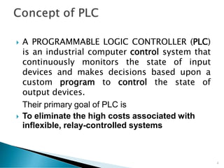
- 1. A PROGRAMMABLE LOGIC CONTROLLER (PLC) is an industrial computer control system that continuously monitors the state of input devices and makes decisions based upon a custom program to control the state of output devices. Their primary goal of PLC is To eliminate the high costs associated with inflexible, relay-controlled systems 4
- 2. Prior to PLCs, many control tasks were performed by contactors, control relays and other electromechanical devices. This is often referred to as hard-wired control. Circuit diagrams had to be designed, electrical components specified and installed, and wiring lists created. If an error was made, the wires had to be reconnected correctly. A change in function or system expansion required extensive component changes and rewiring. Requires periodic maintenance and testing. Relay operation can be affected due to ageing of the components and dust, pollution resulting in spurious trips Operation speed for an electromagnetic relays is limited by the mechanical inertia of the component 10
- 3. Smaller physical size than hard-wire solutions. Easier and faster to make changes. PLCs have integrated diagnostics and override functions. Diagnostics are centrally available. Applications can be immediately documented. Applications can be duplicated faster and less expensively. 11
- 4. 1. SMALL it covers units with up to 128 I/O’s and memories up to 2 Kbytes. 2. MEDIUM They have up to 2048 I/O’s and memories up to 32 Kbytes. 3. LARGE They have up to 8192 I/O’s and memories up to 750 Kbytes. 12
- 5. • Less wiring. • Wiring between devices and relay contacts are done in the PLC program. • Easier and faster to make changes. • Trouble shooting aids make programming easier and reduce downtime. • Reliable components make these likely to operate for years before failure. 19
- 6. Manufacturing / Machining Food / Beverage Metals Power Mining Petrochemical / Chemical 21
- 7. Working of PLC Prepared by Mrs. Alka Kalra
- 8. 23 Major Components of a Common PLC PROCESSOR POWER SUPPLY I M N O P D U U T L E O M U O T D P U U L T E PROGRAMMING DEVICE From SENSORS Pushbuttons, contacts, limit switches, etc. To OUTPUT Solenoids, contactors, alarms etc. Prepared by Alka Kalra
- 9. Read all field input devices via the input interfaces, execute the user program stored in application memory, then, based on whatever control scheme has been programmed by the user, turn the field output devices on or off, or perform whatever control is necessary for the process application. This process of sequentially reading the inputs, executing the program in memory, and updating the outputs is known as scanning. Prepared by Alka Kalra
- 10. PHASE 1 – Input Status scan A PLC scan cycle begins with the CPU reading the status of its inputs. PHASE 2– Logic Solve/Program Execution The application program is executed using the status of the inputs PHASE 3– Logic Solve/Program Execution Once the program is executed, the CPU performs diagnostics and communication tasks PHASE 4 - Output Status Scan An output status scan is then performed, whereby the stored output values are sent to actuators and other field output devices. The cycle ends by updating the outputs. Prepared by Alka Kalra
- 11. As soon as Phase 4 are completed, the entire cycle begins again with Phase 1 input scan. The time it takes to implement a scan cycle is called SCAN TIME. ◦ The scan time composed of the program scan time, which is the time required for solving the control program, and the I/O update time, or time required to read inputs and update outputs. The program scan time generally depends on the amount of memory taken by the control program and type of instructions used in the program. The time to make a single scan can vary from 1 ms to 100 ms Prepared by Alka Kalra
- 12. 27 While the PLC is running, the scanning process includes the following four phases, which are repeated continuously as individual cycles of operation: PHASE 2 Program Execution PHASE 3 Diagnostics/ Comm PHASE 4 Output Scan PHASE 1 Read Inputs Scan Prepared by Alka Kalra
- 13. Prepared by Alka Kalra
- 14. The input sources convert the real-time analog electric signals to suitable digital electric signals and these signals are applied to the PLC through the connector rails. These input signals are stored in the PLC external image memory in locations known as bits. This is done by the CPU The control logic or the program instructions are written onto the programming device through symbols or through mnemonics and stored in the user memory. Prepared by Alka Kalra
- 15. The CPU fetches these instructions from the user memory and executes the input signals by manipulating, computing, processing them to control the output devices. The execution results are then stored in the external image memory which controls the output drives. The CPU also keeps a check on the output signals and keeps updating the contents of the input image memory according to the changes in the output memory. The CPU also performs internal programming functions like setting and resetting of the timer, checking the user memory. Prepared by Alka Kalra
- 16. Prepared by Alka Kalra
- 17. 3 ANSWER : d) All of the above 4. Programmable Logic Controller: 4.1. Introduction: A programmable logic controller (PLC) is a specialized Programmable device which is used to control machines and processes. It uses a programmable memory to store instructions and execute specific functions that include on/off control, timing, counting, sequencing, arithmetic, and data handling. Advantages Increased Reliability More Flexibility Lower Cost Communications Capability Faster Response Time Easier to Troubleshoot 4.2 PLC Block diagram
- 18. Prepared by Alka Kalra
- 19. The basic elements of a PLC include input modules or points, a Central Processing Unit (CPU), output modules or points, and a programming device. The type of input modules or points used by a PLC depend upon the types of input devices used. Some input modules or points respond to digital inputs, also called discrete inputs, which are either on or off. Other modules or inputs respond to analog signals. 6
- 20. PLCs are capable of monitoring the inputs continuously from sensors and producing the output decisions to operate the actuators based on the program. Every PLC system needs at least these three modules: CPU Module Power Supply Module One or more I/O Module Prepared by Alka Kalra
- 21. The primary function of a PLC’s input circuitry is to convert the signals provided by these various switches and sensors into logic signals that can be used by the CPU. The CPU evaluates the status of inputs, outputs, and other variables as it executes a stored program. The CPU then sends signals to update the status of outputs. 7
- 22. CPU module consists of a central processor and its memory. The Processor is responsible for doing all the necessary computations and data processing by accepting the inputs and producing appropriate outputs. Prepared by Alka Kalra
- 23. The main function of the microprocessor is to analyze data coming from field sensors through input modules, make decisions based on the user’s defined control program and return signal back through output modules to the field devices. Field sensors(Input): switches, flow, level, pressure, temp. transmitters, etc. Field output devices: motors, valves, solenoids, lamps, or audible devices. Prepared by Alka Kalra
- 24. These PLCs use retentive memory to save user programs and data when the power supply breaks or fails and to resume the execution of a user program ones the power is restored. Thus, these PLCs do not need any use of a keyboard or monitor for re programming the processor each time. The retentive memory can be implemented with the use of long-life batteries, EEPROM modules and flash memory methods. Prepared by Alka Kalra
- 25. VOLATILE. A volatile memory is one that loses its stored information when power is removed. Even momentary losses of power will erase any information stored or programmed on a volatile memory chip. Common Type of Volatile Memory RAM. Random Access Memory(Read/Write) Prepared by Alka Kalra
- 26. Read/write indicates that the information stored in the memory can be retrieved or read, while write indicates that the user can program or write information into the memory. The words random access refer to the ability of any location (address) in the memory to be accessed or used. Ram memory is used for both the user memory (ladder diagrams) and storage memory in many PLC’s. Prepared by Alka Kalra
- 27. The CMOS-RAM (Complimentary Metal Oxide Semiconductor) is probably one of the most popular. CMOS-RAM is popular because it has a very low current drain when not being accessed (15microamps), and the information stored in memory can be retained by as little as 2Vdc. RAM memory must have battery backup to retain or protect the stored program. Prepared by Alka Kalra
- 28. NON-VOLATILE Has the ability to retain stored information when power is removed, accidentally or intentionally. These memories do not require battery back-up. Common Type of Non-Volatile Memory ROM, Read Only Memory Read only indicates that the information stored in memory can be read only and cannot be changed. Information in ROM is placed there by the manufacturer for the internal use and operation of the PLC. Prepared by Alka Kalra
- 29. PROM, Programmable Read Only Memory Allows initial and/or additional information to be written into the chip. PROM may be written into only once after being received from the PLC manufacturer; programming is accomplish by pulses of current. The current melts the fusible links in the device, preventing it from being reprogrammed. This type of memory is used to prevent unauthorized program changes. Prepared by Alka Kalra
- 30. EPROM, Erasable Programmable Read Only Memory Ideally suited when program storage is to be semi- permanent or additional security is needed to prevent unauthorized program changes. The EPROM chip has a quartz window over a silicon material that contains the electronic integrated circuits. This window normally is covered by an opaque material, but when the opaque material is removed and the circuitry exposed to ultra violet light, the memory content can be erased. The EPROM chip is also referred to as UVPROM. Prepared by Alka Kalra
- 31. Electrically Erasable Programmable Read Only Memory Also referred to as E2PROM, is a chip that can be programmed using a standard programming device and can be erased by the proper signal being applied to the erase pin. EEPROM is used primarily as a non-volatile backup for the normal RAM memory. If the program in RAM is lost or erased, a copy of the program stored on an EEPROM chip can be down loaded into the RAM. Prepared by Alka Kalra
- 32. Processor module includes both ROM and RAM memories. ◦ ROM (Program Memory/System Memory) contains the operating system, driver and application programs, ◦ RAM (Data Memory/Application Memory)stores user- written programs and working data. The program information or the control logic is stored in the user memory or the program memory from where the CPU fetches the program instructions. The input and output signals and the timer and counter signals are stored in the input and output external image memory respectively. Prepared by Alka Kalra
- 33. In some modular PLCs bus or rack is provided in the backplane of the circuit into which all the modules like CPU and other I/O modules are plugged to the corresponding slots. This bus enables the communication between CPU and I/O modules to send or receive the data. This communication is established by addressing the I/O modules according to the location from CPU module along the bus. Prepared by Alka Kalra
- 34. The I/O interface section of a PLC connects it to external field devices. The input and out modules of the programmable logic controller are used to connect the sensors and actuators to the system to sense the various parameters such as temperature, pressure and flow, etc. These I/O modules are of two types: digital or analog. Prepared by Alka Kalra
- 35. • The main purpose of the I/O interface is to condition the various signals received from or sent to the external input and output devices. • Input modules converts signals from discrete or analog input devices to logic levels acceptable to PLC’s processor. • Output modules converts signal from the processor to levels capable of driving the connected discrete or analog output devices. Prepared by Alka Kalra
- 36. Prepared by Alka Kalra OPTO- ISOLATOR IS NEEDED TO: Prevent voltage transients from damaging the processor. Helps reduce the effects of electrical noise Current Limiting Resistor FROM INPUT DEVICE USE TO DROP THE VOLTAGE TO LOGIC LEVEL Buffer, Filter, hysteresis Circuits TO PROCESSOR
- 37. Pilot Duty Outputs Outputs of this type typically are used to drive high-current electromagnetic loads such as solenoids, relays, valves, and motor starters. These loads are highly inductive and exhibit a large current. General - Purpose Outputs These are usually low- voltage and low-current and are used to drive indicating lights and other non-inductive loads. Noise suppression may or may not be included on this types of modules. Discrete Inputs Circuits of this type are used to sense the status of limit switches, push buttons, and other discrete sensors. Noise suppression is of great importance in preventing false indication of inputs turning on or off because of noise. Prepared by Alka Kalra
- 38. Circuits of this type sense or drive analog signals. Analog inputs come from devices, such as thermocouples, strain gages, or pressure sensors, that provide a signal voltage or current that is derived from the process variable. Standard Analog Input signals: 4-20mA; 0-10V Analog outputs can be used to drive devices such as voltmeters, X-Y recorders, servomotor drives, and valves through the use of transducers. Standard Analog Output signals: 4-20mA; 0-5V; 0- 10V Prepared by Alka Kalra
- 39. Circuits of this type are used to interface PLCs to very specific types of circuits such as servomotors, stepping motors PID (proportional plus integral plus derivative) loops, high-speed pulse counting, resolver and decoder inputs, multiplexed displays, and keyboards. This module allows for limited access to timer and counter presets and other PLC variables without requiring a program loader. Prepared by Alka Kalra
- 41. The programming device is used to enter or change the PLC’s program or to monitor or change stored values. Once entered, the program and associated variables are stored in the CPU. In addition to these basic elements, a PLC system may also incorporate an operator interface device of some sort to simplify monitoring of the machine or process. 8
- 42. It is used to enter the desired program that will determine the sequence of operation and control of process equipment or driven machine. Also known as: Industrial Terminal ( Allen Bradley ) Program Development Terminal ( General Electric ) Programming Panel ( Gould Modicon ) Programmer ( Square D ) Program Loader ( Idec-Izumi ) Programming Console ( Keyence / Omron ) Prepared by Alka Kalra
- 43. Various types of programming devices are used to enter, modify and troubleshoot a PLC program. Hand held unit with LED / LCD display Personal Computer (PC) Desktop type with a CRT display /Desktop Console Prepared by Alka Kalra
- 44. In the handheld programming device method, a proprietary device is connected to PLC through a connecting cable. This device consists of a set of keys that allows to enter, edit and dump the code into the PLC. These handheld devices consist of small display to make the instruction that has been programmed visible. These are compact and easy to use devices, but these handheld devices have limited capabilities. Prepared by Alka Kalra
- 45. PC is used for programming the PLC in conjunction with the software given by the manufacturer. By using this PC we can run the program in either online or offline mode, and can also edit, monitor, diagnose and troubleshoot the program of the PLC. The way of transferring the program to the PLC is shown in the above figure wherein the PC consists of program code corresponding to control application which is transferred to the PLC CPU via programming cable. . A major advantage of using a computer is that the program can be stored on the hard disk or a CD and copies can be easily made. Prepared by Alka Kalra
- 46. Changing resident PLC programs - uploading/downloading from a supervisory controller (Laptop or desktop computer). • Forcing I/O points and memory elements from a remote terminal. • Linking a PLC into a control hierarchy containing several sizes of PLC and computer. • Monitoring data and alarms, etc. via printers or Operator Interface Units (OIUs). Prepared by Alka Kalra
- 47. A PLC power supply is the workhorse of the PLC system. It converts your line voltage, 120 or 240 volts AC, to a lower DC voltage, commonly 24 volts DC. This DC voltage is then sent into the rack to power the rest of the PLC components. The output 5V DC drives the computer circuitry, and in some PLCs 24DC on the bus rack drives few sensors and actuators. Prepared by Alka Kalra
- 48. Prepared by Alka Kalra
- 49. Line voltage is stepped down with a transformer, rectified to convert it to DC, filtered with capacitors, and protected during this process. All of this is packed into that small looking power supply. This DC voltage is used to power the rest of the PLC and components. The common current ratings for PLC’s are anywhere from 2 to 10 amps for smaller systems and up to 50 amps for larger, more powerful controllers. Prepared by Alka Kalra
- 50. Number of logical inputs and outputs This specifies the number of I/O devices that can be connected to the controller. There should be sufficient I/O ports to meet present requirements with enough spares to provide for moderate future expansion. Prepared by Alka Kalra
- 51. MEMORY CAPACITY The amount of memory required for a particular application is related to the length of the program and the complexity of the control system. Simple applications having just a few relays do not require significant amount of memory. Program length tend to expand after the system have been used for a while. It is advantageous to a acquire a controller that has more memory than is presently needed. Prepared by Alka Kalra
- 52. OUTPUT-PORT POWER RATINGS Each output port should be capable of supplying sufficient voltage and current to drive the output peripheral connected to it. Scan Time This is the speed at which the controller executes the relay ladder logic program. This variable is usually specified as the scan time per 1000 logic nodes and typically ranges from 1 to 200 milliseconds. Prepared by Alka Kalra
- 53. The difference between a PLC and relay logic is that a PLC is a programmable device where as relay logic is a network of hardwired electrical devices. Both a PLC and relay logic can perform logical computation, but a PLC does it using a microprocessor and relay logic does it using electric circuits 9
- 54. Communications Port RS-232, RS 422 / RS 485,LAN Software 1. Allen-Bradley – Rockwell Software RSLogix500 2. Modicon - Modsoft 3. Omron - Syswin 4. GE-Fanuc Series 6 – LogicMaster6 5. Square D- PowerLogic 6. Texas Instruments – Simatic 6. Telemecanique – Modicon TSX Micro Prepared by Alka Kalra
- 55. A Detailed Design Process 1. Understand the process 2. Hardware/software selection 3. Develop ladder logic 4. Determine scan times and memory requirements PLC Status Indicators 1. Power On 2. Run Mode 3. Programming Mode 4. Fault Prepared by Alka Kalra
- 56. 1. Look at the process 2. PLC status lights HALT - something has stopped the CPU RUN - the PLC thinks it is OK (and probably is) ERROR - a physical problem has occurred with the PLC 3. Indicator lights on I/O cards and sensors 4. Consult the manuals, or use software if available. 5. Use programming terminal / laptop. Prepared by Alka Kalra
- 58. Problem Statement : Providing lubricant for the gear box before the lathe spindle starts to run which aims to ensure that the oil pump motor starts first and the main motor starts subsequently. Number of PLC Inputs Required X0 – START pushbutton to Start Oil Pump Motor X1 – START pushbutton to Stop Main Motor X2 – STOP pushbutton to Stop Oil Pump Motor X3 – STOP pushbutton to Stop Main Motor Number of PLC Outputs Required Y0 – Oil Pump Motor Y1 – Main Motor
- 59. There are only 5 languages that are considered to be standard languages for use on PLCs, according to IEC section 61131–3. Ladder Diagram (LD) A sequential function chart Function Block Diagram Instruction List Structured Text 13
- 60. Ladder Diagram is the oldest PLC language. This graphical programming language was modeled from relay logic to allow engineers and electricians to transition smoothly into programming PLCs. Within Ladder, rungs and rails represent the real world electrical connections. Specifically, the vertical “rails” represent the supply power of the device while the rungs that are connected to the rails are equal to the amount of control circuits. 14
- 61. 4 1. The vertical lines of the diagram represent the power rails between which circuits are connected. The power flow is taken to be from the left-hand vertical across a rung. 2. Each rung on the ladder defines one operation in the control process. 3. A ladder diagram is read from left to right and from top to bottom, showing the scanning motion employed by the PLC. The top rung is read from left to right. Then the second rung down is read from left to right and so on. 4. Each rung must start with an input or inputs and must end with at least one output. The term input is used for a control action, such as closing the contacts of a switch, used as an input to the PLC. The term output is used for a device connected to the output of a PLC, e.g., a motor. 5. Electrical devices are shown in their normal condition. Thus a switch, which is normally open until some object closes it, is shown as open on the ladder diagram. A switch that is normally closed is shown closed.
- 62. 5 6. A particular device can appear in more than one rung of a ladder. For example, we might have a relay that switches on one or more devices. The same letters and/or numbers are used to label the device in each situation. 7. The inputs and outputs are all identified by their addresses, the notation used depending on the PLC manufacturer. This is the address of the input or output in the memory of the PLC. 8.The instructions used are the relay equivalent of normally open (NO) and normally closed (NC) contacts and coils. 9.Contact symbolism is a simple way of expressing the control logic in terms of symbols that are used on relay control schematics. 10.A rung is the contact symbolism required to control an output. Some PLCs allow a rung to have multiple outputs. 11.A complete ladder logic program thus consists of several rungs. each of which controls an output. 12.Because the PLC uses ladder logic diagrams. the conversion from any existing relay logic to programmed logic is simple. 13. Each rung is a combination of input conditions (symbols) connected from left to right, with the symbol that represents the output at the far right. 14.The symbols that represent the inputs are connected in series, parallel. or some combination of the two to obtain the desired logic. 15.Because the PLC uses ladder logic diagrams. the conversion from any existing relay logic to programmed logic is simple. 16. Each rung is a combination of input conditions (symbols) connected from left to right, with the symbol that represents the output at the far right. 17.The symbols that represent the inputs are connected in series, parallel. or some combination of the two to obtain the desired logic. RUNG A type of line diagram that uses the input and output symbols used by PLC ladder logic. Line diagrams are converted to programming diagrams before being entered into a PLC
- 63. This program is a typical application of the conditional control circuit. Y0 = ON when Oil Pump START button is pressed. Therefore, the oil pump will start to provide lubricant for the gear box of main motor(Y1) Under the precondition of the operating state of the Oil pump, the main motor (Y1) will be ON when the Main motor START button is pressed. During the operation of main motor (Y1), oil pump (Y0) needs to provide lubricant continuously. The oil pump will be stopped when Oil pump STOP button X2 is activated, and the main motor will be stopped when Main motor STOP button X3 is activated.
- 64. Problem Statement: Detecting the standing bottles on the conveyor and pushing falling bottles in tray.
- 65. Number of PLC Inputs Required X0 – Proximity Sensor to sense bottom of the Bottle i.e. X0 = ON when the detected input signal from the bottle-bottom is sheltered. X1 – Proximity Sensor to sense upper part of the Bottle i.e. X1 = ON when the detected input signal from the bottle-neck is sheltered. Number of PLC Outputs Required Y0 – To operate Pushing Cylinder/Rod
- 66. A sequential function chart is a graphical programming language that mimics a flow chart. You use steps and transitions to get output. Steps are functions within the program and house events that are activated based on state and other specified conditions. Transitions are instructions based on true/false values that move you from one step to another. Branches are used to initiate multiple steps at a time. The branches act like threads where functions can run concurrently. All of these steps, transitions, and branches are housed in a series of scripts that execute in a procedural manner. The visual nature of the language allows users to monitor processes that both heavily use conditional logic and run parallel instructions. PLCs that are prone to suffering from bottlenecks can be more intuitively maintained and troubleshooted using the chart to follow the logic of the program. 15
- 67. This is the PLC’s equivalent to assembly language. This gives you immediate access to the machine itself, which allows you to write code that is compressed and fast. The code is represented in the manner that the language’s name suggests: in a list of commands. Structured Text is a high level language designed to program PLCs. This is essentially the C++ of the PLC world. Any PLC that requires complex data handling will most likely use ST. 17
- 68. Block based programming languages are a type of graphical language that minimizes code into blocks, which allows for a simple way to create executable commands. FBD in particular describes a function between inputs and outputs that are connected by connection lines. The logic of the inputs and outputs are stored in blocks. The blocks are programmed onto sheets and the PLC scans these sheets in order or by specified connections between blocks, much like procedural languages. The I/O focus mirrors that of ladder logic. Yet, the code that the blocks contain allow engineers to develop more complex batch control tasks among other repeatable tasks. 16
- 69. If the bottle on the conveyor belt is upstanding, the input signal from monitoring photocell at both bottle-bottom and bottle- neck will be detected. In this case, X0 = ON, and X1 = ON. The normally open (NO) contact X0 will be activated as well as the normally closed (NC) contact X1. Y0 remains OFF and pneumatic pushing pole will not perform any action. If the bottle from the conveyor belt is down, only the input signal from monitoring photocell at the bottle-bottom will be detected. In this case, X0 = ON, X1 = OFF. The state of output YO will be ON because the NO contact X0 activates and the NC contact X1 remains OFF. The pneumatic pushing pole will push the fallen bottle out of the conveyor belt.
- 70. Structured Text is a high level language designed to program PLCs. This is essentially the C++ of the PLC world. Any PLC that requires complex data handling will most likely use ST. 18
- 71. 6 4.2 PLC Instructions RELAY-TYPE INSTRUCTIONS The ladder diagram language is basically a symbolic set of instructions used to create the controller program. The three fundamental symbols that are used to translate relay control logic to contact symbolic logic are EXAMINE IF CLOSED,EXAMINE IF OPEN, and OUTPUT ENERGIZE Normally open Analogous to the normally open relay contact. For this instruction. we ask the processor to EXAMINE IF (the contact is) CLOSED. The status bit will be either1(ON) or 0 (OFF) The status bit is examined for an ON condition. If the status bit is I (ON). Then the instruction is TRUE.
- 72. 7 If the status bit is 0 (OFF). Then the instruction is FALSE. Normally closed instruction, we ask the processor to EXAMINE IF (the contact is) OPEN. The status bit will be either 1 (ON) or 0 (OFF). The status bit is examined for an OFF condition. If the status bit is 0 (OFF), then the instruction is TRUE. It the status bit is 1 (ON), then the Instruction is FALSE.
- 73. 8 Relay coil (OTE) The processor ( makes it is Instruction true (analogous to energizing a coil) when there is a path 01 true XIC and XIO instructions in the rung. If any left to right path of input conditions is TRUE. the output is energized (turned ON). The status bit 01 the addressed OUTPUT Energize instruction is set to 1 (ON) when the rung is TRUE.
- 74. 10 Parallel input Branching Input branching by formation of parallel branches can be used in your application pro- gram to allow more than one combination of input conditions, If at least one of these parallel branches forms a true logic path, the rung logic is enabled. If none of the parallel branches forms a true logic path. rung logic is not enabled and the output instruction logic will not be TRUE. In the example shown, either A and B or C provides a true logical path. Parallel input Branching with Output branching branches can be established at both input and output portions of a rung. With output branching. you can Program parallel outputs on a rung to allow a true logic path to control multiple outputs. When there is a true logic path. all parallel outputs become TRUE. either A or B provides a true logical path to all three output instructions: C, D, and E. Parallel output branching with input
- 75. 11 Additional input logic instructions (conditions) can be programmed in the output branches to enhance condition contra) of the outputs. When there is a true logic path, including extra input conditions on an output branch. That branch becomes TRUE. either A and D or Band D provide a true logic path to E. Nested Input and output branches can be nested to avoid redundant instructions and to speed up processor scan time. Input and output branches can be nested to avoid redundant instructions and to speed up processor scan time. 4.3. Implementation of logic gates using ladder AND Logic It is a basic gate. Whenever the all the input condition must true then output becomes true Figure (a)Truth table of the AND logic (b) block diagram of AND logic
- 76. 12 Logic equation Ladder Logic diagram for AND Logic OR LOGIC It is basic gate. Whenever any one of the input conditions is true the output becomes true
- 77. 13 Figure (a)Truth table of the OR logic (b) block diagram of OR logic Logic equation Y= A+B Ladder logic diagram of the OR logic Two limit switches connected in parallel and used to control a solenoid valve. NOT logic It is one of the basic logic gate output always the complement of input Truth Table of NOT logic Ladder logic diagram of NOT logic
- 78. 14 NAND LOGIC It is an universal gate. Whenever the all the input must true condition the output becomes false or If any one of the inputs is false condtion then output becomes true. Truth Table of the NAND Logic Logic Equation of the NAND Logic Ladder Logic diagram for NAND logic
- 79. 15 NOR Logic It is an universal gate. Whenever all the input conditions are false then output becomes true TRUTH TABLE of the NOR logic LOGIC equation Ladder logic diagram for NOR logic Exclusive OR The output of this circuit is ON only when pushbutton A or B is pressed, but not both. Case 1When A= 0 and B= 0: Let us analyze main rung. When I1 = 0, the normally open instruction is false and, normally closed instruction is true, but since normally open instruction is false, there is no logical continuity and output cannot be energized. Similar analysis can be done in parallel
- 80. 16 rung, normally closed instruction will be true and normally open instruction will be false and output is not energized. Case 2When A= 0 and B = 1: In main rung, normally open instruction will be false and, normally closed instruction will be true, but since there is no logical continuity this rung logic cannot energize the output. But, in parallel rung, normally closed instruction will be true, as well as normally open instruction will also be true, hence there is logical continuity, and output is energized. Case 3 When I1 = 1 and I2 = 0: This case is similar to case 2, only the role of inputs are interchanged i.e. here main rung is true and energizes the output and parallel rung is false. Case 4 When both inputs are true, the main ladder rung as well as the parallel ladder rung goes false. In main rung, normally open instruction is true but normally closed instruction is false. Hence, there is no logical continuity. In parallel ladder rung, normally closed instruction is false and normally open instruction is true, and here also there is no logical continuity. Hence, the output is not energized.
- 81. 17 Latch circuit There are often situations where it is necessary to hold an output energized, even when the input ceases. A simple example of such a situation is a motor, which is started by pressing a push button switch. Though the switch contacts do not remain closed, the motor is required to continue running until a stop push button switch is pressed. The term latch circuit is used for the circuit used to carry out such an operation. It is a self-maintaining circuit in that, after being energized, it maintains that state until another input is received. 4.4.Simple Programs A lighting control system is to be developed. The system will be controlled by four switches, SWITCH1, SWITCH2, SWITCH3, and SWITCH4. These switches will control the lighting in a room based on the following criteria: 1. Any of three of the switches SWITCH1, SWITCH2, and SWITCH3, if turned ON can turn the lighting on, but all three switches must be OFF before the lighting will turn OFF. 2. The fourth switch SWITCH4 is a Master Control Switch. If this switch is in the ON position, the lights will be OFF and none of the other three switches have any control. Design the wiring diagram for the controller connections, assign the inputs and outputs and develop the ladder diagram which will accomplish the task. Number of PLC Inputs Required INPUT IN1 = SWITCH1 INPUT IN2 = SWITCH2 INPUT IN3 = SWITCH3 INPUT IN4 = SWITCH4 (Master Control Switch)
- 82. 18 Number of PLC Outputs Required OUTPUT OUT1 = Lights control relay coil CR1 Any of three of the switches SWITCH1, SWITCH2, and SWITCH3, if turned ON can turn the lighting on The fourth switch SWITCH4 is a Master Control Switch. If this switch is in the ON position, the lights will be OFF Boolean logic CR1=(IN1 OR IN2 OR IN3) AND IN4 5. POST MCQ 1. Function Block Diagram (FBD) is a type of____________. a) PLC Language
- 83. 17 1) Computer with SIMATIC software. 2) Siemens S7-1200 PLC. 3) LEDs. 4) Switches. 5) Connecting wires THEORY TIMERS On-Delay Timer The On-Delay Timer (TON) instruction counts time when the enabling input is ON. When the current value (Txxx) is greater than or equal to the present time (PT), the timer bit is ON. The On-Delay timer current value is cleared when the enabling input is OFF. This timer continues counting after the Preset is reached, and it stops counting at the maximum value of 32767. The timer shown in figure will delay for 1000*1ms= 1000ms = 1 second then it will be activated ON. Here when you activate the input I0.0, the timer T37 starts delaying time, until it reaches 1000ms, then T37 bit turns ON, hence Q0.0 will be ON. As a result Q0.0 will be activated after 1 second activating I0.0. Ladder logic diagram for on-delay timer. the timing diagram
- 84. 20 the count-up input CU makes the transition from off to on. When the current value (Cxxx) is greater than or equal to the Preset Value (PV), the counter bit (Cxxx) turns on. The counter is reset when the Reset (R) input turns on, or when the Reset instruction is executed. The counter stops counting when it reaches the maximum value (32,767). Counter ranges: Cxxx=C0 through C255 Count Down Counter The Count Down (CTD) instruction counts down from the current value of that counter each time the countdown input CD makes the transition from off to on. When the current value Cxxx is equal to zero, the counter bit (Cxxx) turns on. The counter resets the counter bit (Cxxx) and loads the current value with the preset value (PV) when the load input (LD) turns on. The Down Counter stops counting when it reaches zero, and the counter bit Cxxx turns on. Counter ranges: Cxxx=C0 through C255
- 85. 19 (Ladder logic diagram for off-delay timer. The timing diagram) COUNTER Count Up Counter The Count Up (CTU) instruction counts up from the current value each time
- 86. 18 Off-Delay Timer The Off-Delay Timer (TOF) is used to delay turning an output OFF for a fixed period of time after the input turns OFF. When the enabling input turns ON, the timer bit turns ON immediately, and the current value is set to 0. When the input turns OFF, the timer counts until the elapsed time reaches the preset time. When the preset is reached, the timer bit turns OFF and the current value stops counting. If the input is OFF for a time shorter than the preset value, the timer bit remains ON. The TOF instruction must see an ON to OFF transition to begin counting.
- 87. 21 PROCEDURE: 1. Turn the PC ON. 2. Turn the PLC ON. 3. Start V4.0 STEP 7 Micro WIN SP5. 4. Select View>>Ladder. 5. Form Bit Logic double, click the normally open contact. 6. Click on the red question marks, and rename the normally open contactor with a physical input name, I0.0- I0.7 or I1.0-I1.5, let us say I0.0. 7. Now from the Bit Logic, double click the output, and name it with a physical output name, Q0.0-Q0.7 or Q1.0-Q1.1, let us say Q0.0, the result rung will be as shown in the next figure. 8. Select PLC>>Compile All; make sure that the "Total Errors" is zero. 9. Select PLC>>STOP to place the PLC in the stop mode. 10. To download the ladder diagram to the PLC, click download (shown to the right), the window for downloading appears then click to download. 11. Now place the PLC in the run mode, by selecting PLC>>RUN. 12. Now the PLC is ready for use performing the function of the ladder diagram that you have drawn. Conclusion: This is all about different timer and counter using PLC ladder programming. As well as PLC programming rules and programming instructions are also important for writing the program. …………………………………………………………………………………
- 88. PLC Ladder Practice Problem: The production line may be powered off accidentally or turned off for noon break. The program is to control the counter to retain the counted number and resume counting after the power is turned ON again. When the daily production reaches 500, the target completed indicator will be ON to remind the operator for keeping a record. Press the Clear button to clear the history records. The counter will start counting from 0 again.
- 89. Latched 16 bit UP counter Number of PLC Inputs Required X0 – Product Detecting Sensor. X1 – Production Counter RESET/Clear Number of PLC Outputs Required Y0 – Production Counter Target Completed. Number of PLC Counter Required: C120 – 16 Bit Latched Counter. (Max Count =32,768)
- 90. The latching counter is demanded for the situation of retaining data when power-off. When a product is completed, C120 will count for one time. When the number reaches 500, target completed indicator Y0 will be ON. For different series of PLC, the setup range of 16-bit latching counter is different.
- 91. Enabling the indicator to be ON immediately when switch pressed and OFF after a 5 sec delay by the switch.
- 92. Number of PLC Inputs Required X1 – Start Switch. Number of PLC Outputs Required Y1 – Output Indicator Number of PLC Timer Required T0 – 5 second Timer, 100 ms Time Base. (See K50 Preset Value for Timer) When X1 = ON, TMR instruction will be executed. Timer T1 will be ON and start counting for 3 sec. When T1 reaches its set value, the NO (Normally Open) contact T1 will be activated and indicator YI will be ON. When X1 = OFF, TMR instruction will not be executed. Timer T1 will be OFF and so will NO contact T1. Therefore, the indicator Y1 will be OFF.
- 94. A practical application for a comparative function is something called alternating motor control, where the run- times of two redundant electric motors are monitored, with the PLC determining which motor to turn on next based on which motor has run the least
- 95. In this program, two retentive on-delay timers keep track of each electric motor’s total run time, storing the run time values in two registers in the PLC’s memory: Motor A runtime and Motor B runtime. These two integer values are input to the “greater than” instruction box for comparison. If motor A has run longer than motor B, motor B will be the one enabled to start up next time the “start” switch is pressed. If motor A has run less time or the same amount of time as motor B (the scenario shown by the blue-highlighted status indications), motor A will be the one enabled to start. The two series-connected virtual contacts OUT motor A and OUT motor B ensure the comparison between motor run times is not made until both motors are stopped. If the comparison were continually made, a situation might arise where both motors would start if someone happened to press the Start pushbutton with one motor is already running.
- 98. 27 Execute Ladder diagrams with model applications (i) Stair case lighting (ii) Traffic light controller AIM: Execute Ladder diagrams with model applications Stair case lighting. Equipment: I0.0 & I0.1: Input toggle switches. Q0.0: Output signaling device. THEORY; This ladder logic of stair-case wiring works on the X-OR logic i.e.Y is (A.B^) + (A^. B) Suppose initially only I0.0 is pressed and I0.1 remains open physically as shown then the upper branch of rung 1 goes TRUE and Q0.0 gets energized. Now, if I0.0 is also pressed then it will make its interlock N-C contact I0.1 to go open and as a result Q0.0 de-energizes . Again, if switch I0.0 is pressed it will also make its interlock contact I0.0 in parallel branch to go again N-C, which in turn makes the parallel branch logic true and Q0.0 again energizes but if the I0.1 input is also pressed again the logic goes FALSE and Q0.0 again de-energizes. This is the basic concept of an X-OR logic gate. .
- 99. 28 PROCEDURE: For this application, we used S7-1200 PLC and TIA portal software for programming. In above program, we have added two NO contacts of SW 1 (I0.1) and SW 2 (I0.2) in series and NC contacts of SW1 (I0.1) and SW2 (I0.2) in parallel of this series SW1 & SW2 NO Contacts. If the status of the bottom switch (SW1) and status of the top switch (SW2) are same then lamp will be ON. And if either status of the bottom or top switch is different from other then lamp (Q0.0) will be OFF. When lamp (Q0.0) is OFF then user can ON the lamp by changing status of any switch. Also user can turn OFF the lamp by changing the status of one of the two switches. List of inputs/outputs Digital Inputs SW1 : I0.1 SW2 : I0.2 Digital Outputs Lamp : Q0.0 PLC Ladder diagram for two ways switch logic
- 100. 29 Runtime Test Cases CONCLUSION: The above PLC Logic provided for basic idea about application of PLC for Stair case lighting Two Way Switch Logic. ……………………………………………………………………………………….
- 103. They are so many ways to write a program for traffic light control ex: sequencer output method but in this normal input, outputs and timers are used. Timers are used to give time delay for output to turn ON and OFF. Reset coil is used at the end to run the program continuously. Comparator blocks are used to reduce the number of timers used.
- 105. 22 Execute the Ladder Diagrams with model applications (i) DOL starter (ii)Star- Delta starter AIM: Execute the Ladder Diagrams with model applications (i) DOL starter (ii)Star- Delta starter THEORY Star Delta Motor Starter The following figure shows the winding connections in star and delta configuration one by one. It can be seen that in star connection, one end of all three windings are shorted to make star point while other end of each winding is connected to power supply. In delta configuration, the windings are connected such that to make a close loop. The connection of each winding is shown in above figure. In actual motor the three phase connections are provided in the following order as shown
- 106. 23 So in order to make winding connection in star and delta style in practical motor, the connection is shown above. Main contractor is used to supply power to the windings. It must be turned on all the time. Initially the star contactor is closed while delta contactor is open It makes the motor windings in star configuration. The contactors are controlled by using PLC. The following section of PLC tutorial will explain the ladder programming for star delta motor starter. PROCEDURE PLC program for star delta motor starter:
- 107. 24 PLC Ladder Logic Rung 1 Main contactor : The main contactor depends upon the normally open input start push button (I1), normally closed stop button (I2) and normally closed overload relay. It means that Main contactor will only be energized if start button is pressed, while stop is not pressed and overload relay is not activated. A normally open input named (Q1) is added in parallel to the start button I1. By doing so, a push button is created which means that once motor is started, it will be kept started even if start button is released
- 108. 25 Rung 2 Star contactor: Star contactor depends upon main contactor, normally close contacts of timer (T1), and normally close contacts of output delta contactor (Q3). So star contactor will only be energized if main contactor is ON, time output is not activated and delta contactor is not energized. Timer T1: Timer T1 measures the time after which the winding connection of star delta starter is to be changed. It will start counting time after main contractor is energized. Rung 3 Delta contactor: Delta contactor will be energized when main contactor (Q1) is energized, timer T1 is activated and star contactor (Q3) is de-energized. Also see Programming of push button and other requirements for simple motor starter is explained in PLC Tutorial: Motor starter DOL Starter Ladder Diagram The ladder diagram of the dol starter.dol (Direct-On-Line) starter is used to start the motor by applying full line voltage to the motor. Dol starter is used for the motors having rating up to the 05HP. Figure shows the control diagram of the dol starter.
- 109. One method of starting electric motors is using direct on line (DOL) or across the line starter. In this method full line voltage is applied to the motor terminals. This is simplest type of motor starter.
- 110. DOL motor starter contains fuse and over load relay (OLR) for protection purpose. The starter can be contain momentary contact or maintained contact push buttons. The example considered here is momentary contact push buttons. For starting purpose normally open (NO) push button is preferred whereas normally closed (NC) push button is used to stop the motor. The excessive supply voltage drop causing high inrush current is the criteria to limit the use of DOL starter. Conveyor motors, water pumps are the applications where DOL starters are used.
- 112. Listing of Input and Output devices: Inputs: PB1- To start the motor PB2- To stop the motor Output: M1- Motor 1. When Start push button (PB1) is pressed, Motor (M1) has to start. 2. If Start pushbutton (PB1) is released and Stop pushbutton (PB2) is not pressed, Motor (M1) should remain on. 3. When Stop push button (PB2 is pressed, Motor (M1) has tol stop. 4. If stop push button is released and start is not pressed (released) motor shouldl remain off.
- 114. Micro Controller Series (MCS)-51 Over View
- 115. The microprocessor is the core of computer systems. Nowadays many communication, digital entertainment, portable devices, are controlled by them. A designer should know what types of components he needs, ways to reduce production costs and product reliable. Hardware :Interface to the real world Software :order how to deal with inputs
- 116. CPU: Central Processing Unit I/O: Input /Output Bus: Address bus & Data bus Memory: RAM & ROM Timer Interrupt Serial Port Parallel Port
- 117. CPU General- Purpose Micro- processor RAM ROM I/O Port Timer Serial COM Port Data Bus Address Bus CPU for Computers No RAM, ROM, I/O on CPU chip itself Example:Intel’s 8085,8086, Motorola’s 680x0 Many chips on mother’s board General-purpose microprocessor
- 118. Microprocessor CPU is stand-alone, RAM, ROM, I/O, timer are separate Designer can decide on the amount of ROM, RAM and I/O ports. expansive versatility general-purpose Microcontroller • CPU, RAM, ROM, I/O and timer are all on a single chip • fix amount of on-chip ROM, RAM, I/O ports • for applications in which cost, power and space are critical • single-purpose
- 119. 4K bytes internal ROM 128 bytes internal RAM Four 8-bit I/O ports (P0 - P3). Two 16-bit timers/counters One serial interface RAM I/O Port Timer Serial COM Port Microcontroller CPU A single chip ROM
- 120. CPU Interrupt Control OSC Bus Control 4k ROM Timer 1 Timer 2 Serial 128 bytes RAM 4 I/O Ports TXD RXD External Interrupts P0 P2 P1 P3 Addr/Data
- 121. only 1 On chip oscillator (external crystal) 6 interrupt sources (2 external , 3 internal, Reset) 64K external code (program) memory(only read)PSEN 64K external data memory(can be read and write) by RD,WR Code memory is selectable by EA (internal or external) We may have External memory as data and code
- 122. 89XX ROM RAM Timer Int Source IO pin Other 8951 4k 128 2 6 32 - 8952 8k 256 3 8 32 - 8953 12k 256 3 9 32 WD 8955 20k 256 3 8 32 WD 898252 8k 256 3 9 32 ISP 891051 1k 64 1 3 16 AC 892051 2k 128 2 6 16 AC WD: Watch Dog Timer AC: Analog Comparator ISP: In System Programable
- 123. meeting the computing needs of the task efficiently and cost effectively ◦ speed, the amount of ROM and RAM, the number of I/O ports and timers, size, packaging, power consumption ◦ easy to upgrade ◦ cost per unit availability of software development tools ◦ assemblers, debuggers, C compilers, emulator, simulator, technical support wide availability and reliable sources of the microcontrollers
- 125. One of the most useful features of the 8051 is that it contains four I/O ports (P0 - P3) Port 0 (pins 32-39):P0(P0.0~P0.7) ◦ 8-bit R/W - General Purpose I/O ◦ Or acts as a multiplexed low byte address and data bus for external memory design Port 1 (pins 1-8) :P1(P1.0~P1.7) ◦ Only 8-bit R/W - General Purpose I/O Port 2 (pins 21-28):P2(P2.0~P2.7) ◦ 8-bit R/W - General Purpose I/O ◦ Or high byte of the address bus for external memory design Port 3 (pins 10-17):P3(P3.0~P3.7) ◦ General Purpose I/O ◦ if not using any of the internal peripherals (timers) or external interrupts. Each port can be used as input or output (bi-direction)
- 126. PSEN (out): Program Store Enable, the read signal for external program memory (active low). ALE (out): Address Latch Enable, to latch address outputs at Port0 and Port2 EA (in): External Access Enable, active low to access external program memory locations 0 to 4K RXD,TXD: UART pins for serial I/O on Port 3 XTAL1 & XTAL2: Crystal inputs for internal oscillator. Vcc(pin 40): ◦ Vcc provides supply voltage to the chip. ◦ The voltage source is +5V. GND(pin 20):ground
- 127. RST(pin 9: Reset ◦ input pin and active high(normally low). The high pulse must be high at least 2 machine cycles. ◦ Power-on reset Upon applying a high pulse to RST, the microcontroller will reset and all values in registers will be lost. Reset values of some 8051 registers
- 129. 8051 Internal Block Diagram
- 130. 8 bit CPU with registers A and B 16 bit PC and DPTR(data pointer). 8 bit program status word(PSW) 8 bit Stack Pointer 32 I/O pins arranged as 4 8 bit ports:P0 to P3 Two 16 bit timer/counters:T0 and T1 Full duplex serial data receiver/transmitter Control registers : TCON,TMOD,SCON,PCON,IP and IE Two external and Three internal interrupt sources. Oscillator and Clock Circuits. 4K Internal ROM 128bytes Internal RAM - 4 register banks each having 8 registers 16 bytes, which may be addressed at the bit level. 80 bytes of general purpose data memory Wednesday, November 1, 2023
- 132. 07 06 05 04 03 02 01 00 R7 R6 R5 R4 R3 R2 R1 R0 0F 08 17 10 1F 18 Bank 3 Bank 2 Bank 1 Bank 0 Four Register Banks Each bank has R0-R7 Selectable by psw.2,3
- 133. Four banks of 8 byte-sized registers, R0 to R7 Addresses are : 18 - 1F for bank 3 10 - 17 for bank 2 08 - 0F for bank 1 00 - 07 for bank 0 (default) Active bank selected by bits [ RS1, RS0 ] in PSW. Permits fast “context switching” in interrupt service routines (ISR).
- 134. A B R0 R1 R3 R4 R2 R5 R7 R6 DPH DPL PC DPTR PC Some 8051 16-bit Register Some 8-bit Registers of the 8051
- 135. It is used as a general register to accumulate the results of a large number of instructions. It can hold an 8-bit (1-byte) value and is the most versatile register the 8051 has due to the shear number of instructions that make use of the accumulator. More than half of the 8051’s 255 instructions manipulate or use the accumulator in some way.
- 136. The "R" registers are a set of eight registers that are named R0, R1, etc. up to and including R7. These registers are used as auxiliary registers in many operations The "R" registers are also used to temporarily store values. For example, let’s say you want to add the values in R1 and R2 together and then subtract the values of R3 and R4. One way to do this would be: MOV A,R3 ;Move the value of R3 into the accumulator ADD A,R4 ;Add the value of R4 MOV R5,A ;Store the resulting value temporarily in R5 MOV A,R1 ;Move the value of R1 into the accumulator ADD A,R2 ;Add the value of R2 SUBB A,R5 ;Subtract the value of R5 (which now contains R3 + R4)
- 137. The "B" register is very similar to the Accumulator in the sense that it may hold an 8-bit (1-byte) value. The "B" register is only used by two 8051 instructions: MUL AB and DIV AB. Thus, if you want to quickly and easily multiply or divide A by another number, you may store the other number in "B" and make use of these two instructions.
- 138. The Data Pointer (DPTR) is the 8051’s only user- accessable 16-bit (2-byte) register. The Accumulator, "R" registers, and "B" register are all 1-byte values. DPTR, as the name suggests, is used to point to data. It is used by a number of commands which allow the 8051 to access external memory. DPTR is most often used to point to data in external memory.
- 139. The Program Counter (PC) is a 2-byte address which tells the 8051 where the next instruction to execute is found in memory. When the 8051 is initialized PC always starts at 0000h and is incremented each time an instruction is executed. It is important to note that PC isn’t always incremented by one. Since some instructions require 2 or 3 bytes the PC will be incremented by 2 or 3 in these cases.
- 140. The Stack Pointer, like all registers except DPTR and PC, may hold an 8-bit (1-byte) value. The Stack Pointer is used to indicate where the next value to be removed from the stack should be taken from. When a value is push onto the stack, the 8051 first increments the value of SP and then stores the value at the resulting memory location.
- 142. Wednesday, November 1, 2023 Port 0(pins 32-39) When connecting an 8051 to an external memory, the 8051 uses ports to send addresses and read instructions. ◦ 16-bit address:P0 provides both address A0-A7, P2 provides address A8-A15. ◦ Also, P0 provides data lines D0-D7. When P0 is used for address/data multiplexing, it is connected to the 74LS373 to latch the address. Port 1(pins 1-8) Port 1 is denoted by P1. ◦ P1.0 ~ P1.7 ◦ P1 as an output port (i.e., write CPU data to the external pin) ◦ P1 as an input port (i.e., read pin data into CPU bus)
- 143. Wednesday, November 1, 2023 Although port 3 is configured as an output port upon reset, this is not the way it is most commonly used. Port 3 has the additional function of providing signals. ◦ Serial communications signal:RxD, TxD ◦ External interrupt:/INT0, /INT1 ◦ Timer/counter:T0, T1 ◦ External memory accesses :/WR, /RD
- 144. The 8051 microcontroller's memory is divided into Program Memory and Data Memory. Program Memory (ROM) is used for permanent saving program being executed, Data Memory (RAM) is used for temporarily storing and keeping intermediate results and variables.
- 145. Program Memory (ROM) is used for permanent saving program (CODE) being executed. The memory is read only. Depending on the settings made in compiler, program memory may also used to store a constant variables. The 8051 executes programs stored in program memory only. Code memory type specifier is used to refer to program memory. 8051 memory organization allows external program memory to be added. How does the microcontroller handle external memory depends on the pin EA logical state.
- 147. Up to 256 bytes of internal data memory is available Locations available to the user occupy addressing space from 0 to 7Fh, i.e. first 128 registers and this part of RAM is divided in several blocks. The first 128 bytes of internal data memory are both directly and indirectly addressable. The upper 128 bytes of data memory (from 0x80 to 0xFF) can be addressed only indirectly.
- 148. Wednesday, November 1, 2023 RAM memory space allocation in the 8051 7FH 30H 2FH 20H 1FH 17H 10H 0FH 07H 08H 18H 00H Register Bank 0 (Stack) Register Bank 1 Register Bank 2 Register Bank 3 Bit-Addressable RAM Scratch pad RAM Memory Organization
- 149. Memory block in the range of 20h to 2Fh is bit-addressable, which means that each bit being there has its own address from 0 to 7Fh. Since there are 16 such registers, this block contains in total of 128 bits with separate addresses ( Bit 0 of byte 20h has the bit address 0, and bit 7 of byte 2Fh has the bit address 7Fh).
- 150. Access to external memory is slower than access to internal data memory. There may be up to 64K Bytes of external data memory. Several 8051 devices provide on-chip XRAM space that is accessed with the same instructions as the traditional external data space. This XRAM space is typically enabled via proper setting of SFR register and overlaps the external memory space. Setting of that register must be manually done in code, before any access to external memory or XRAM space is made.
- 154. SFRs which are also bit addressable A, B, IP, IE, TCON, SCON, PSW, P0, P1, P2, P3 Other SFRs TMOD, THO, TLO, TH1, TL1, SBUF, PCON, SP, DPTR
- 155. DATA registers CONTROL registers Timers Serial ports Interrupt system Analog to Digital converter Digital to Analog converter Etc. Addresses 80h – FFh Direct Addressing used to access SPRs
- 156. Name Function Name Function A Accumulator SBUF Serial Port data buffer B Arithmetic SP Stack Pointer DPH Addressing Ext Memory TMOD Timer/Counter mode cntrl DPL Addressing Ext Memory TCON Timer/Counter cntrl IE Interrupt enable TL0 Timer0 lower byte IP Interrupt Priority TH0 Timer0 higher byte P0 I/O Port Latch TL1 Timer1 lower byte P1 I/O Port Latch TH1 Timer1 higher byte P2 I/O Port Latch P3 I/O Port Latch PCON Power Control
- 159. Gate : When set, timer only runs while INT(0,1) is high. C/T : Counter/Timer select bit. M1 : Mode bit 1. M0 : Mode bit 0.
- 160. TF1: Timer 1 overflow flag. TR1: Timer 1 run control bit. TF0: Timer 0 overflag. TR0: Timer 0 run control bit. IE1: External interrupt 1 edge flag. IT1: External interrupt 1 type flag. IE0: External interrupt 0 edge flag. IT0: External interrupt 0 type flag.
- 161. Instruction Set and Addressing Modes of 8051
- 162. Sunday, August 23, 2020 Immediate Register Direct Register Indirect Indexed The way in which the instruction is specified.
- 163. Sunday, August 23, 2020 Immediate Data is specified in the instruction itself Egs: MOV A,#65H MOV A,#’A’ MOV R6,#65H MOV DPTR,#2343H MOV P1,#65H
- 164. Sunday, August 23, 2020 MOV Rn, A ;n=0,..,7 ADD A, Rn MOV DPL, R6 MOV DPTR, A MOV Rm, Rn
- 165. Sunday, August 23, 2020 Although the entire of 128 bytes of RAM can be accessed using direct addressing mode, it is most often used to access RAM loc. 30 – 7FH. MOV R0, 40H MOV 56H, A MOV A, 4 ; ≡ MOV A, R4 MOV 6, 2 ; copy R2 to R6 ; MOV R6,R2 is invalid !
- 166. Sunday, August 23, 2020 In this mode, register is used as a pointer to the data. MOV A,@Ri ; move content of RAM loc. Where address is held by Ri into A ( i=0 or 1 ) MOV @R1,B In other word, the content of register R0 or R1 is sources or target in MOV, ADD and SUBB insructions. ⌦ jump
- 167. Sunday, August 23, 2020 This mode is widely used in accessing data elements of look-up table entries located in the program (code) space ROM at the 8051 MOVC A,@A+DPTR A= content of address A +DPTR from ROM Note: Because the data elements are stored in the program (code ) space ROM of the 8051, it uses the instruction MOVC instead of MOV. The “C” means code.
- 169. Data transfer instructions Addressing modes Data processing (arithmetic and logic) Program flow instructions
- 170. MOV dest, source dest 🡨 source Stack instructions PUSH byte ;increment stack pointer, ;move byte on stack POP byte ;move from stack to byte, ;decrement stack pointer Exchange instructions XCH a, byte ;exchange accumulator and byte XCHD a, byte ;exchange low nibbles of ;accumulator and byte
- 171. Immediate Mode – specify data by its value mov A, #0 ;put 0 in the accumulator ;A = 00000000 mov R4, #11h ;put 11hex in the R4 register ;R4 = 00010001 mov B, #11 ;put 11 decimal in b register ;B = 00001011 mov DPTR,#7521h ;put 7521 hex in DPTR ;DPTR = 0111010100100001
- 172. Immediate Mode – continue MOV DPTR,#7521h MOV DPL,#21H MOV DPH, #75 COUNT EGU 30 ~ ~ mov R4, #COUNT MOV DPTR,#MYDATA ~ ~ 0RG 200H MYDATA:DB “IRAN”
- 173. Register Addressing – either source or destination is one of CPU register MOV R0,A MOV A,R7 ADD A,R4 ADD A,R7 MOV DPTR,#25F5H MOV R5,DPL MOV R,DPH Note that MOV R4,R7 is incorrect
- 174. Direct Mode – specify data by its 8-bit address Usually for 30h-7Fh of RAM Mov a, 70h ; copy contents of RAM at 70h to a Mov R0,40h ; copy contents of RAM at 70h to a Mov 56h,a ; put contents of a at 56h to a Mov 0D0h,a ; put contents of a into PSW
- 175. Direct Mode – play with R0-R7 by direct address MOV A,4 ≡ MOV A,R4 MOV A,7 ≡ MOV A,R7 MOV 7,2 ≡ MOV R7,R6 MOV R2,#5 ;Put 5 in R2 MOV R2,5 ;Put content of RAM at 5 in R2
- 176. Register Indirect – the address of the source or destination is specified in registers Uses registers R0 or R1 for 8-bit address: mov psw, #0 ; use register bank 0 mov r0, #0x3C mov @r0, #3 ; memory at 3C gets #3 ; M[3C] 🡨 3 Uses DPTR register for 16-bit addresses: mov dptr, #0x9000 ; dptr 🡨 9000h movx a, @dptr ; a 🡨 M[9000] Note that 9000 is an address in external memory
- 177. Register Indexed Mode – source or destination address is the sum of the base address and the accumulator(Index) Base address can be DPTR or PC mov dptr, #4000h mov a, #5 movc a, @a + dptr ;a 🡨 M[4005]
- 178. A register can be accessed by direct and register mode This 3 instruction has same function with different code 0703 E500 mov a,00h 0705 8500E0 mov acc,00h 0708 8500E0 mov 0e0h,00h Also this 3 instruction 070B E9 mov a,r1 070C 89E0 mov acc,r1 070E 89E0 mov 0e0h,r1
- 179. B – always direct mode - except in MUL & DIV 0703 8500F0 mov b,00h 0706 8500F0 mov 0f0h,00h 0709 8CF0 mov b,r4 070B 8CF0 mov 0f0h,r4 P0~P3 – are direct address 0704 F580 mov p0,a 0706 F580 mov 80h,a 0708 859080 mov p0,p1 Also other SFRs (pcon, tmod, psw,….)
- 180. Op code Direct address Op code Immediate data immediate addressing add a,#3dh ;machine code=243d Direct addressing mov r3,0E8h ;machine code=ABE8
- 181. Stack-oriented data transfer – Only one operand (direct addressing) – SP is other operand – register indirect - implied Direct addressing mode must be used in Push and Pop mov sp, #0x40 ; Initialize SP push 0x55 ; SP 🡨 SP+1, M[SP] 🡨 M[55] ; M[41] 🡨 M[55] pop b ; b 🡨 M[55] Note: can only specify RAM or SFRs (direct mode) to push or pop. Therefore, to push/pop the accumulator, must use acc, not a
- 182. Therefore Push a ;is invalid Push r0 ;is invalid Push r1 ;is invalid push acc ;is correct Push psw ;is correct Push b ;is correct Push 13h Push 0 Push 1 Pop 7 Pop 8 Push 0e0h ;acc Pop 0f0h ;b
- 183. Serial communication means transfer data bit by bit serially at a time, where as in parallel communication, the number of bits that can be transferred at a time depends upon the number of data lines available for communication. Two methods of serial communication are Synchronous Communication: Transfer of bulk data in framed structure at a time Asynchronous Communication: Transfer of a byte data in framed structure at a time 8051 has built in UART with RXD (serial data receive pin) and TXD (serial data transmit pin) on PORT3.0 and PORT3.1 respectively.
- 185. Asynchronous serial communication is widely used for byte oriented transmission. Frame structure in Asynchronous communication: START bit: It is a bit with which serial communication start and it is always low. Data bits packet: Data bits can be 5 to 9 bits packet. Normally we use 8 data bit packet, which is always sent after START bit. STOP bit: This is one or two bits. It is sent after data bits packet to indicate end of frame. Stop bit is always logic high. In asynchronous serial communication frame, first START bit followed by data byte and at last STOP bit, forms a 10-bit frame. Sometimes last bit is also used as parity bit.
- 186. Data transmission rate is measured in bits per second (bps). In binary system it is also called as baud rate (number of signal changes per second). Standard baud rates supported are 1200, 2400, 4800, 19200, 38400, 57600, and 115200. Normally most of the time 9600 bps is used when speed is not a big issue.
- 187. SBUF: Serial Buffer Register This is the serial communication data register used to transmit or receive data through it. SCON: Serial Control Register Serial control register SCON is used to set serial communication operation modes. Also it is used to control transmit and receive operations.
- 188. Mode SM0 SM1 Mode 0 0 0 1/12 of Osc frequency shift register mode fixed baud rate 1 0 1 8-bit UART with timer 1 determined baud rate 2 1 0 9-bit UART with 1/32 of Osc fixed baud rate 3 1 1 9-bit UART with timer 1 determined baud rate Bit 7:6 - SM0:SM1: Serial Mode Specifier Normally mode-1 (SM0 =0, SM1=1) is used with 8 data bits, 1 start bit and 1 stop bit.
- 189. Bit 5 - SM2: for Multiprocessor Communication This bit enables multiprocessor communication feature in mode 2 & 3. Bit 4 - REN: Receive Enable 1 = Receive enable 0 = Receive disable Bit 3 - TB8: 9th Transmit Bit This is 9th bit which is to be transmitted in mode 2 & 3 (9-bit mode) Bit 2 - RB8: 9th Receive Bit This is 9th received bit in mode 2 & 3 (9-bit mode), where as in mode 1, if SM2 = 0 then RB8 hold stop bit that received Bit 1 - TI: Transmit Interrupt Flag This bit indicates transmission is complete and gets set after transmitting the byte from buffer. Normally TI (Transmit Interrupt Flag) is set by hardware at the end of 8th bit in mode 0 and at the beginning of stop bit in other modes. Bit 0 – RI: Receive Interrupt Flag This bit indicates reception is complete and gets set after receiving the complete byte in buffer. Normally RI (Receive Interrupt Flag) is set by hardware in receiving mode at the end of 8th bit in mode 0 and at the stop bit receive time in other modes.
- 190. The 8051 has two counters/timers which can be used either as timer to generate a time delay or as counter to count events happening outside the microcontroller. he 8051 has two timers: timer0 and timer1. They can be used either as timers or as counters. Both timers are 16 bits wide. Since the 8051 has an 8-bit architecture, each 16- bit is accessed as two separate registers of low byte and high byte.
- 191. Timer0 registers is a 16 bits register and accessed as low byte and high byte. The low byte is referred as a TL0 and the high byte is referred as TH0. These registers can be accessed like any other registers.
- 192. Timer1 registers is also a 16 bits register and is split into two bytes, referred to as TL1 and TH1.
- 193. This is an 8-bit register which is used by both timers 0 and 1 to set the various timer modes. In this TMOD register, lower 4 bits are set aside for timer0 and the upper 4 bits are set aside for timer1 In upper or lower 4 bits, first bit is a GATE bit. Every timer has a means of starting and stopping. Some timers do this by software, some by hardware, and some have both software and hardware controls. The hardware way of starting and stopping the timer by an external source is achieved by making GATE=1 in the TMOD register. And if we change to GATE=0 then we do no need external hardware to start and stop the timers.
- 194. The second bit is C/T bit and is used to decide whether a timer is used as a time delay generator or an event counter. If this bit is 0 then it is used as a timer and if it is 1 then it is used as a counter. In upper or lower 4 bits, the last bits third and fourth are known as M1 and M0 respectively. These are used to select the timer mode. M0 M1 Mode Operating Mode 0 0 0 13-bit timer mode, 0 1 1 16-bit timer mode, 1 0 2 8-bit auto reload 1 1 3 Spilt timer mode.
- 195. TCON is 8-bit control register and contains timer and interrupt flags. Bit 7 - TF1: Timer1 Overflow Flag 1 = Timer1 overflow occurred (i.e. Timer1 goes to its max and roll over back to zero). 0 = Timer1 overflow not occurred. It is cleared through software. In Timer1 overflow interrupt service routine, this bit will get cleared automatically while exiting from ISR. Bit 6 - TR1: Timer1 Run Control Bit 1 = Timer1 start. 0 = Timer1 stop. It is set and cleared by software. Bit 5 – TF0: Timer0 Overflow Flag 1 = Timer0 overflow occurred (i.e. Timer0 goes to its max and roll over back to zero). 0 = Timer0 overflow not occurred. It is cleared through software. In Timer0 overflow interrupt service routine, this bit will get cleared automatically while exiting from ISR.
- 196. Bit 4 – TR0: Timer0 Run Control Bit 1 = Timer0 start. 0 = Timer0 stop. It is set and cleared by software. Bit 3 - IE1: External Interrupt1 Edge Flag 1 = External interrupt1 occurred. 0 = External interrupt1 Processed. It is set and cleared by hardware. Bit 2 - IT1: External Interrupt1 Trigger Type Select Bit 1 = Interrupt occur on falling edge at INT1 pin. 0 = Interrupt occur on low level at INT1 pin. Bit 1 – IE0: External Interrupt0 Edge Flag 1 = External interrupt0 occurred. 0 = External interrupt0 Processed. It is set and cleared by hardware. Bit 0 – IT0: External Interrupt0 Trigger Type Select Bit 1 = Interrupt occur on falling edge at INT0 pin. 0 = Interrupt occur on low level at INT0 pin.
- 197. Interrupts in 8051 microcontroller are more desirable to reduce the regular status checking of the interfaced devices or inbuilt devices. Interrupt is an event that temporarily suspends the main program, passes the control to a special code section, executes the event-related function and resumes the main program flow where it had left off.
- 198. Interrupts are of different types like software and hardware, maskable and non-maskable, fixed and vector interrupts, and so on. Interrupt Service Routine (ISR) comes into the picture when interrupt occurs, and then tells the processor to take appropriate action for the interrupt, and after ISR execution, the controller jumps into the main program.
- 199. 8051 has 5 sources of interrupts – Timer 0 overflow(T0) – Timer 1 overflow(T1) – External Interrupt 0(INT0) – External Interrupt 1(INT1) – Serial Port events(TI/RI) – The Timer and Serial interrupts are internally generated by the microcontroller, whereas the external interrupts are generated by additional interfacing devices or switches that are externally connected to the microcontroller. These external interrupts can be edge triggered or level triggered. When an interrupt occurs, the microcontroller executes the interrupt service routine so that memory location corresponds to the interrupt that enables it. The Interrupt corresponding to the memory location is given in the interrupt vector table below.
- 200. What if two interrupt sources interrupt at the same time? The interrupt with the highest PRIORITY gets serviced first. All interrupts have a default priority order. Priority can also be set to “high” or “low”.
- 202. This register is responsible for enabling and disabling the interrupt. It is a bit addressable register in which EA must be set to one for enabling interrupts. The corresponding bit in this register enables particular interrupt like timer, external and serial inputs. In the below IE register, bit corresponding to 1 activates the interrupt and 0 disables the interrupt.
- 203. This register is responsible for enabling and disabling the interrupt. It is a bit addressable register in which EA must be set to one for enabling interrupts. The corresponding bit in this register enables particular interrupt like timer, external and serial inputs. In the below IE register, bit corresponding to 1 activates the interrupt and 0 disables the interrupt.
- 204. ▪EA : Global enable/disable. ▪--- : Undefined. ▪ET2 :Enable Timer 2 interrupt. ▪ES :Enable Serial port interrupt. ▪ET1 :Enable Timer 1 interrupt. ▪EX1 :Enable External 1 interrupt. ▪ET0 : Enable Timer 0 interrupt. ▪EX0 : Enable External 0 interrupt.
- 205. It is also possible to change the priority levels of the interrupts by setting or clearing the corresponding bit in the Interrupt priority (IP) register as shown in the figure. This allows the low priority interrupt to interrupt the high-priority interrupt, but prohibits the interruption by another low-priority interrupt. Similarly, the high-priority interrupt cannot be interrupted. If these interrupt priorities are not programmed, the microcontroller executes in predefined manner and its order is INT0, TF0, INT1, TF1, and SI.
- 208. Operation:MOV Function:Move memory Syntax:MOV operand1,operand2 Description: MOV copies the value of operand2 into operand1. The value of operand2 is not affected. Both operand1 and operand2 must be in Internal RAM. No flags are affected unless the instruction is moving the value of a bit into the carry bit in which case the carry bit is affected or unless the instruction is moving a value into the PSW register (which contains all the program flags).
- 209. No flags are affected unless the instruction is moving the value of a bit into the carry bit in which case the carry bit is affected or unless the instruction is moving a value into the PSW register (which contains all the program flags). MOV @R0,#data MOV @R0,A MOV A,#data MOV A,@R1 MOV A,R0
- 210. two way data transfer XCH a, 30h ; a 🡨 🡨 M[30] XCH a, R0 ; a 🡨 🡨 R0 XCH a, @R0 ; a 🡨 🡨 M[R0] XCHD a, R0 ; exchange “digit” R0[7..4] R0[3..0] a[7..4] a[3..0] Only 4 bits exchanged
- 211. transfers between individual bits. Carry flag (C) (bit 7 in the PSW) is used as a single- bit accumulator RAM bits in addresses 20-2F are bit addressable mov C, P0.0 mov C, 67h mov C, 2ch.7
- 212. SFRs with addresses ending in 0 or 8 are bit- addressable. (80, 88, 90, 98, etc) Notice that all 4 parallel I/O ports are bit addressable.
- 213. Subroutines allow us to have "structured" assembly language programs. This is useful for breaking a large design into manageable parts. It saves code space when subroutines can be called many times in the same program. Main: ... acall sublabel ... ... sublabel: ... ... ret the subroutine
- 214. square: push b mov b,a mul ab pop b ret 8 byte and 11 machine cycle SP is initialized to 07 after reset.(Same address as R7) With each push operation 1st , pc is increased When using subroutines, the stack will be used to store the PC, so it is very important to initialize the stack pointer. Location 2Fh is often used. mov SP, #2Fh
- 215. mov a,#0aah Back1:mov p0,a lcall delay1 cpl a sjmp back1 Delay1:mov r0,#0ffh;1cycle Here: djnz r0,here ;2cycle ret ;2cycle end Delay=1+255*2+2=513 cycle Delay2: mov r6,#0ffh back1: mov r7,#0ffh ;1cycle Here: djnz r7,here ;2cycle djnz r6,back1;2cycle ret ;2cycle end Delay=1+(1+255*2+2)*255+2 =130818 machine cycle
- 216. Mnemonic Description ADD A, byte add A to byte, put result in A ADDC A, byte add with carry SUBB A, byte subtract with borrow INC A increment A INC byte increment byte in memory INC DPTR increment data pointer DEC A decrement accumulator DEC byte decrement byte MUL AB multiply accumulator by b register DIV AB divide accumulator by b register DA A decimal adjust the accumulator
- 217. add a, byte ; a 🡨 a + byte addc a, byte ; a 🡨 a + byte + C These instructions affect 3 bits in PSW: C = 1 if result of add is greater than FF AC = 1 if there is a carry out of bit 3 OV = 1 if there is a carry out of bit 7, but not from bit 6, or visa versa.
- 219. mov a, #3Fh add a, #D3h What is the value of the C, AC, OV flags after the second instruction is executed? 0011 1111 1101 0011 0001 0010 C = 1 AC = 1 OV = 0
- 220. 0111 1111 (positive 127) 0111 0011 (positive 115) 1111 0010 (overflow cannot represent 242 in 8 bits 2’s complement) 2’s complement: 0000 0000 00 0 … 0111 1111 7F 127 1000 0000 80 -128 … 1111 1111 FF -1 1000 1111 (negative 113) 1101 0011 (negative 45) 0110 0010 (overflow) 0011 1111 (positive) 1101 0011 (negative) 0001 0010 (never overflows)
- 221. ; Computes Z = X + Y ; Adds values at locations 78h and 79h and puts them in 7Ah ;-------------------------------------------------------------- ---- X equ 78h Y equ 79h Z equ 7Ah ;-------------------------------------------------------------- --- org 00h ljmp Main ;-------------------------------------------------------------- --- org 100h Main: mov a, X add a, Y mov Z, a end
- 222. ; Computes Z = X + Y (X,Y,Z are 16 bit) ;------------------------------------------------------ ------------ X equ 78h Y equ 7Ah Z equ 7Ch ;------------------------------------------------------ ----------- org 00h ljmp Main ;------------------------------------------------------ ----------- org 100h Main: mov a, X add a, Y mov Z, a mov a, X+1 adc a, Y+1 mov Z+1, a end
- 223. SUBB A, byte subtract with borrow Example: SUBB A, #0x4F ;A 🡨 A – 4F – C Notice that There is no subtraction WITHOUT borrow. Therefore, if a subtraction without borrow is desired, it is necessary to clear the C flag. Example: Clr c SUBB A, #0x4F ;A 🡨 A – 4F
- 224. The increment and decrement instructions do NOT affect the C flag. Notice we can only INCREMENT the data pointer, not decrement. INC A increment A INC byte increment byte in memory INC DPTR increment data pointer DEC A decrement accumulator DEC byte decrement byte
- 225. Assume 16-bit word in R3:R2 mov a, r2 add a, #1 ; use add rather than increment to affect C mov r2, a mov a, r3 addc a, #0 ; add C to most significant byte mov r3, a
- 226. When multiplying two 8-bit numbers, the size of the maximum product is 16-bits FF x FF = FE01 (255 x 255 = 65025) MUL AB ; BA 🡨 A * B Note : B gets the High byte A gets the Low byte
- 227. Integer Division DIV AB ; divide A by B A 🡨 Quotient(A/B) B 🡨 Remainder(A/B) OV - used to indicate a divide by zero condition. C – set to zero
- 228. DA a ; decimal adjust a Used to facilitate BCD addition. Adds “6” to either high or low nibble after an addition to create a valid BCD number. Example: mov a, #23h mov b, #29h add a, b ; a 🡨 23h + 29h = 4Ch (wanted 52) DA a ; a 🡨 a + 6 = 52
- 229. ❑ Bitwise logic operations ❖ (AND, OR, XOR, NOT) ❑ Clear ❑ Rotate ❑ Swap Logic instructions do NOT affect the flags in PSW
- 230. ANL 🡨 AND ORL 🡨 OR XRL 🡨 XOR CPL 🡨 Complement Examples: 0000111 1 1010110 0 ANL 0000111 1 1010110 0 ORL 0000111 1 1010110 0 XRL 1010110 0 CPL 0000110 0 1010111 1 1010001 1 0101001 1
- 231. a, byte direct, reg. indirect, reg, immediate byte, a direct byte, #constant a ex: cpl a ANL – AND ORL – OR XRL – eXclusive oR CPL – Complement
- 232. Force individual bits low, without affecting other bits. anl PSW, #0xE7 ;PSW AND 11100111 Force individual bits high. orl PSW, #0x18 ;PSW OR 00011000 Complement individual bits xrl P1, #0x40 ;P1 XRL 01000000
- 233. CLR - clear RL – rotate left RLC – rotate left through Carry RR – rotate right RRC – rotate right through Carry SWAP – swap accumulator nibbles
- 234. CLR A CLR byte (direct mode) CLR Ri (register mode) CLR @Ri (register indirect mode)
- 235. Rotate instructions operate only on a RL a Mov a,#0xF0 ; a🡨 11110000 RR a ; a🡨 11100001 RR a Mov a,#0xF0 ; a🡨 11110000 RR a ; a🡨 01111000
- 236. RRC a mov a, #0A9h ; a 🡨 A9 add a, #14h ; a 🡨 BD (10111101), C🡨 0 rrc a ; a 🡨 01011110, C🡨 1 RLC a mov a, #3ch ; a 🡨 3ch(00111100) setb c ; c 🡨 1 rlc a ; a 🡨 01111001, C🡨 1 C C
- 237. Note that a shift left is the same as multiplying by 2, shift right is divide by 2 mov a, #3 ; A🡨 00000011 (3) clr C ; C🡨 0 rlc a ; A🡨 00000110 (6) rlc a ; A🡨 00001100 (12) rrc a ; A🡨 00000110 (6)
- 238. SWAP a mov a, #72h ; a 🡨 27h swap a ; a 🡨 27h
- 239. Some logic operations can be used with single bit operands ANL C, bit ORL C, bit CLR C CLR bit CPL C CPL bit SETB C SETB bit “bit” can be any of the bit-addressable RAM locations or SFRs.
- 240. Program segment to multiply by 2 and add 1.
- 241. Unconditional jumps (“go to”) Conditional jumps Call and return
- 242. SJMP <rel addr> ; Short jump, relative address is 8-bit 2’s complement number, so jump can be up to 127 locations forward, or 128 locations back. LJMP <address 16> ; Long jump AJMP <address 11> ; Absolute jump to anywhere within 2K block of program memory JMP @A + DPTR ; Long indexed jump
- 243. Start: mov C, p3.7 mov p1.6, C sjmp Start Microcontroller application programs are almost always infinite loops!
- 244. Memory specific NOT Re-locatable (machine code) org 8000h Start: mov C, p1.6 mov p3.7, C ljmp Start end Re-locatable (machine code) org 8000h Start: mov C, p1.6 mov p3.7, C sjmp Start end
- 245. Mov dptr,#jump_table Mov a,#index_number Rl a Jmp @a+dptr ... Jump_table: ajmp case0 ajmp case1 ajmp case2 ajmp case3
- 246. These instructions cause a jump to occur only if a condition is true. Otherwise, program execution continues with the next instruction. loop: mov a, P1 jz loop ; if a=0, goto loop, ; else goto next instruction mov b, a There is no zero flag (z) Content of A checked for zero on time
- 247. Mnemonic Description JZ <rel addr> Jump if a = 0 JNZ <rel addr> Jump if a != 0 JC <rel addr> Jump if C = 1 JNC <rel addr> Jump if C != 1 JB <bit>, <rel addr> Jump if bit = 1 JNB <bit>,<rel addr> Jump if bit != 1 JBC <bir>, <rel addr> Jump if bit =1, &clear bit CJNE A, direct, <rel addr> Compare A and memory, jump if not equal
- 248. jz led_off Setb P1.6 sjmp skipover led_off: clr P1.6 mov A, P0 skipover: if (a = 0) is true send a 0 to LED else send a 1 to LED
- 249. Mnemonic Description CJNE A, #data <rel addr> Compare A and data, jump if not equal CJNE Rn, #data <rel addr> Compare Rn and data, jump if not equal CJNE @Rn, #data <rel addr> Compare Rn and memory, jump if not equal DJNZ Rn, <rel addr> Decrement Rn and then jump if not zero DJNZ direct, <rel addr> Decrement memory and then jump if not zero
- 250. For A = 0 to 4 do {…} clr a loop: ... ... inc a cjne a, #4, loop For A = 4 to 0 do {…} mov R0, #4 loop: ... ... djnz R0, loop
- 251. mov a,#50h mov b,#00h cjne a,#50h,next mov b,#01h next: nop end mov a,#25h mov r0,#10h mov r2,#5 Again: mov @ro,a inc r0 djnz r2,again end mov a,#0h mov r4,#12h Back: add a,#05 djnz r4,back mov r5,a end mov a,#0aah mov b,#10h Back1:mov r6,#50 Back2:cpl a djnz r6,back2 djnz b,back1 end
- 252. Call is similar to a jump, but – Call pushes PC on stack before branching acall <address ll> ; stack 🡨 PC ; PC 🡨 address 11 bit lcall <address 16> ; stack 🡨 PC ; PC 🡨 address 16 bit
- 253. Return is also similar to a jump, but – Return instruction pops PC from stack to get address to jump to ret ; PC 🡨 stack
- 255. Assembly language programming Data Transfer operations Input/Output operations
- 256. The assembly language is a fully hardware related programming language. The embedded designers must have sufficient knowledge on hardware of particular processor or controllers before writing the program. The assembly language is developed by mnemonics; therefore, users cannot understand it easily to modify the program.
- 258. The assembly code must be written in upper case letters The labels must be followed by a colon (label:) All symbols and labels must begin with a letter All comments are typed in lower case The last line of the program must be the END directive
- 259. The assembling directives give the directions to the CPU. The 8051 microcontroller consists of various kinds of assembly directives to give the direction to the control unit. The most useful directives are 8051 programming, such as: ORG DB EQU END
- 260. ORG(origin): This directive indicates the start of the program. This is used to set the register address during assembly. For example; ORG 0000h tells the compiler all subsequent code starting at address 0000h. Syntax: ORG 0000h DB(define byte): The define byte is used to allow a string of bytes. For example, print the “EDGEFX” wherein each character is taken by the address and finally prints the “string” by the DB directly with double quotes. Syntax: ORG 0000h MOV a, #00h ————- DB”EDGEFX”
- 261. EQU (equivalent): The equivalent directive is used to equate address of the variable. Syntax: reg equ,09h —————– —————– MOV reg,#2h END:The END directive is used to indicate the end of the program. Syntax: reg equ,09h —————– —————– MOV reg,#2h END
- 262. An Assembly language program consists of, among other things, a series of lines of Assembly language instructions. An Assembly language instruction consists of a mnemonic, optionally followed by one or two operands. The operands are the data items being manipulated, and the mnemonics are the commands to the CPU, telling it what to do with those items.
- 265. MOV destination, source. Data movement in the internal RAM. This type of instructions supported by virtually all addresses, direct, indirect, recording and immediate. MOV A,P0 ; Mueve el contenido del puerto 0 al acumulador MOV R1,A ; Mueve el contenido del Acumulador al registro 1 MOVX. Data movement in the external RAM (XRAM). This type of motion only supports indirect addressing, register 8bit by R0 or R1 and 16-bit register via the DPTR. MOV DPTR,#2000H ; Mover al registro apuntador DPTR el dato inmediato 2000H (dirección) MOVX A,@DPTR ; Mover el contenido de la memoria que apunta el DPTR (2000H) al Acumulador MOVC. Allows movement of the accumulator ROM. By this statement can make the manipulation or movement of tables from the program memory. XCH. Swaps the contents of the accumulator and the internal RAM. XCHD. Swaps the contents of the first 4 bits of the Accumulator with internal RAM. PUSH and POP. To transfer data to the stack.
- 266. Computers transfer data in two ways: parallel and serial. In parallel data transfers, often 8 or more lines (wire conductors) are used to transfer data to a device that is only a few feet away. Examples of parallel transfers are printers and hard disks; each uses cables with many wire strips. Although in such cases a lot of data can be transferred in a short amount of time by using many wires in parallel, the distance cannot be great. To transfer to a device located many meters away, the serial method is used. In serial communication, the data is sent one bit at a time, in contrast to parallel communication, in which the data is sent a byte or more at a time. Serial communication of the 8051 is the topic of this chapter. The 8051 has serial communication capability built into it, thereby making possible fast data transfer using only a few wires.
- 267. When a microprocessor communicates with the outside world, it provides the data in byte-sized chunks. In some cases, such as printers, the information is simply grabbed from the 8-bit data bus and presented to the 8-bit data bus of the printer. This can work only if the cable is not too long, since long cables diminish and even distort signals. Furthermore, an 8-bit data path is expensive. For these reasons, serial communication is used for transferring data between two systems located at distances of hundreds of feet to millions of miles apart. Figure 10-1 diagrams serial versus parallel data transfers.
- 268. The fact that serial communication uses a single data line instead of the 8-bit data line of parallel communication not only makes it much cheaper but also enables two computers located in two different cities to communicate over the telephone .For serial data communication to work, the byte of data must be converted to serial bits using a parallel-in-serial-out shift register; then it can be transmitted over a single data line. This also means that at the receiving end there must be a serial-in-parallel-out shift register to receive the serial data and pack them into a byte.
- 269. Serial data communication uses two methods, asynchronous and synchronous. The synchronous method transfers a block of data (characters) at a time, while the asynchronous method transfers a single byte at a time. It is possible to write software to use either of these methods, but the programs can be tedious and long. For this reason, there are special 1C chips made by many manufacturers for serial data communications
- 270. . These chips are commonly referred to as UART (universal asynchronous receiver-transmitter) and USART (universal synchronous-asynchronous receiver-transmitter).
- 271. Data transfer instructions are responsible for transferring data between various memory storing elements like registers, RAM, and ROM. The execution time of these instructions varies based on how complex an operation they have to perform. In the table given in next slides, we have listed all the data transfer instruction. In the table [A]= Accumulator; [Rn]=Register in RAM; DPTR=Data Pointer; PC=Program Counter Lets take all these Data Transfer instructions one by one.