1/34
M.S. Registration Seminar
ELECTRONICTRANSPORT IN CARBON
NANOTUBE JUNCTIONS
Under the supervision of: Dr. T.K. Bhattacharyya
Dept. of E&ECE, IIT Kharagpur
Advanced Technology Development Centre
IIT Kharagpur
Srijeet Tripathy
Roll No.- 12AT71P03
2.
Contents
• Introduction: CarbonNanotubes; Electronic properties
• CNT-CNT Junctions (Literature review)
• Proposed Study
• Summary and Future work
• Bibliography
• Appendices
2/34
3.
Since their firstdiscovery and fabrication in 1991,
CNTs have received considerable attention because of
the prospect of new fundamental science and many
potential applications.
Courtesy: Cees Dekker, Delft, Nature 1998
Courtesy: L Jensen, UCB, Nature 2008
Courtesy: A bachtold, ICN, Nature 2012
CNT Devices
Courtesy: E. Snow, NR Lab, APL, 2003 3/34
4.
Avouris, IBM
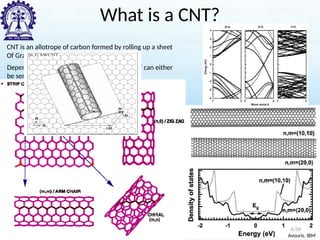
What isa CNT?
CNT is an allotrope of carbon formed by rolling up a sheet
Of Graphene
Depending on the way it is rolled(chirality) CNT can either
be semiconducting or metallic
4/34
5.
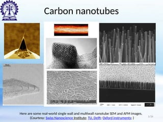
Carbon nanotubes
Here aresome real-world single wall and multiwall nanotube SEM and AFM images.
(Courtesy: Swiss Nanoscience Institute; TU, Delft; Oxford instruments; ) 5/34
6.
6
Motivation
• In theend CNTs must form junctions with other
CNTs or other materials to form multimedial devices
and, ultimately, complex circuits.
• Experimental feasibility
• Electronic and other physical properties of such
junctions must be studied.
6/34
7.
7
• Consist oftwo individual SWNT’s or small bundles
(diameter<3nm) of SWNTs coupled to each other
with two or four electrical contacts, one on each
end of each SWNT or bundle. [Furher, Science
2000]
CNT-CNT Junctions
• This type of junction is easily constructed and, with
the development of techniques to place nanotubes
with precision on substrates, could be mass
produced.
7/34
8.
CNT-CNT Junctions
Courtesy: Postma,Phys. Rev. B 2000 Courtesy: Park, J. Appl. Phys. 2003
Courtesy: Furher, Science 2000
• SWNT junctions can be composed of:
– Two metallic SWNTs (MM)
– One metallic and one semiconducting (MS)
– Two semiconducting SWNTs (SS)
8/34
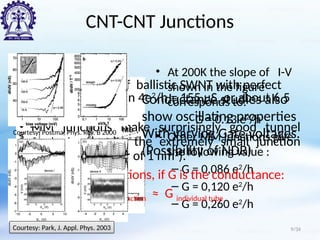
9.
CNT-CNT Junctions
• At200K the slope of I-V
shown in the figure
corresponds to:
G = 0.13 e2
/h
• Other MM junctions give
the following value :
– G = 0,086 e2
/h
– G = 0,120 e2
/h
– G = 0,260 e2
/h
M.S. Furher, Science, 2000
•The conductance of ballistic SWNT with perfect
contacts (T=1) is then 4e2
/h = 155 µS, or about 6.5
kΩ.
• MM junctions make surprisingly good tunnel
contacts, despite the extremely small junction
area (on the order of 1 nm2
).
• Thus, in MM junctions, if G is the conductance:
G junction ≈ G individual tube
Courtesy: Park, J. Appl. Phys. 2003
Courtesy: Postma, Phys. Rev. B 2000
Conductance studies also
show oscillating properties
With varying Gate voltages.
(Possibility of NDR)
9/34
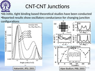
10.
CNT-CNT Junctions
Nakanishi, JPSJ,2001 Alper Budlum, PRB, 2003
•Ab initio, tight binding based theoretical studies have been conducted
•Reported results show oscillatory conductance for changing junction
configurations
10/34
11.
CNT-CNT Junctions
Alper Budlum,PRB, 2003
For parallel coupled junctions Increase
of contact length reveals two types of
short and long wave oscillations
11/34
The oscillations in conductance are attributed to the interference of the
transmitted and reflected Fermi waves flowing through the tubes
12.
12/34
Problem Definition
•Origin ofthe small wave and long wave oscillations
remain unclear
•Overlap dependant conductance may have
interesting applications
•NDR effects with changing gate voltage are yet to be
studied
Theoretical study of such junctions and
Comprehensive study of their electrical
properties
Electronic structure Methods
•Ab initio
• Semi empirical
Due to Computational and time constraints
semi-empirical methods seem to be the appropriate
choice
14/34
15.
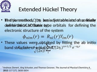
Extended Hückel Theory
•In this method, the basis set consists of a linear
combination of Slater type orbitals for defining the
electronic structure of the system
• The parameters , are adjustable and essentially
define the LCAO basis set
• These values were obtained by fitting the ab initio
band structure of a (6,6)CNT*
*Andreas Zienert, Jörg Schuster, and Thomas Gessner, The Journal of Physical Chemistry A
2013 117 (17), 3650-3654
15/34
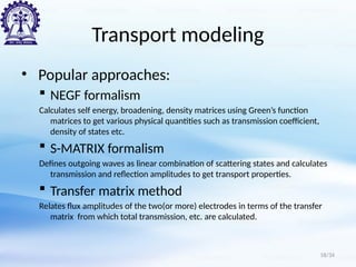
Transport modeling
• Popularapproaches:
NEGF formalism
Calculates self energy, broadening, density matrices using Green’s function
matrices to get various physical quantities such as transmission coefficient,
density of states etc.
S-MATRIX formalism
Defines outgoing waves as linear combination of scattering states and calculates
transmission and reflection amplitudes to get transport properties.
Transfer matrix method
Relates flux amplitudes of the two(or more) electrodes in terms of the transfer
matrix from which total transmission, etc. are calculated.
18/34
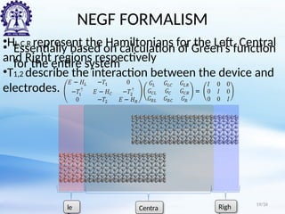
19.
NEGF FORMALISM
• Essentiallybased on calculation of Green’s function
for the entire system
19/34
le Centra Righ
•HL,C,R represent the Hamiltonians for the Left, Central
and Right regions respectively
•T1,2 describe the interaction between the device and
electrodes.
20.
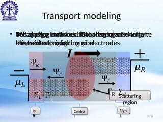
Transport modeling
• Thesystem is divided into three parts:
left, central, right
le
ft
Centra
l
Righ
t 20/34
• We apply a bias such that electrons flow from
the Left to the right region
I
Scattering
region
• Broadening matrices : Broadening of energy
levels due to coupling of electrodes
• Self energy matrices : Coupling of semi infinite
electrodes
21.
Landauer formula
• Currentcalculation : Landauer formula
G (ES H ) 1
A i [G G
]
i [
]
( ) L R
T E G G
k
(k) 2
L
mL
R
L
Conducting
channel
R
L
fR
fL
21/34
22.
Calculated Results
Fig: Transmissionspectra for quarter wavelength(l/4) at zero applied potential.
[Inset: Conductance oscillations for increasing overlap].
Fig.: Calculated current v/s changing overlap length for different applied voltages.
Fig: Conductance oscillations showing both long and short wave oscillations
22/34
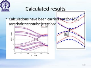
#17 (6,6) armchair band structure has to be added.
#19 The electron distribution in a device configuration. The left and right regions have an equilibrium electron distribution with chemical potentials ul and ur related through the applied sample bias, eVb. The electrons with energies in the bias window ul<e<ur, give rise to a steady state electrical current. The figure illustrates a left moving scattering state with origin in the right electrode.
#20 After setting up a bias, the electrons incident on the junction are partly transmitted and partly reflected across it. Due to the overlap between the tubes, there is a possibility of interference between the incident transmitted and reflected waves.


![7
• Consist of two individual SWNT’s or small bundles
(diameter<3nm) of SWNTs coupled to each other
with two or four electrical contacts, one on each
end of each SWNT or bundle. [Furher, Science
2000]
CNT-CNT Junctions
• This type of junction is easily constructed and, with
the development of techniques to place nanotubes
with precision on substrates, could be mass
produced.
7/34](https://image.slidesharecdn.com/reistrationseminar-new-250331073323-6d808be3/85/Reistration-seminar-new-MS-registration-7-320.jpg)


![Methodology
E1
E2
E3
Pseudo-1D
periodicity
[1] Define unit cell
[2] Assemble
Hamiltonian [H]
[3] Diagonalize H ()
Junction Unit
cell
[4]Calculate Det [EI-H] to
get dispersion relation (E(k))
16/34](https://image.slidesharecdn.com/reistrationseminar-new-250331073323-6d808be3/85/Reistration-seminar-new-MS-registration-16-320.jpg)
![Landauer formula
• Current calculation : Landauer formula
G (ES H ) 1
A i [G G
]
i [
]
( ) L R
T E G G
k
(k) 2
L
mL
R
L
Conducting
channel
R
L
fR
fL
21/34](https://image.slidesharecdn.com/reistrationseminar-new-250331073323-6d808be3/85/Reistration-seminar-new-MS-registration-21-320.jpg)
![Calculated Results
Fig: Transmission spectra for quarter wavelength(l/4) at zero applied potential.
[Inset: Conductance oscillations for increasing overlap].
Fig.: Calculated current v/s changing overlap length for different applied voltages.
Fig: Conductance oscillations showing both long and short wave oscillations
22/34](https://image.slidesharecdn.com/reistrationseminar-new-250331073323-6d808be3/85/Reistration-seminar-new-MS-registration-22-320.jpg)