
Recommended
Recommended
More Related Content
What's hot
What's hot (20)
Similar to NXP 65 V LDMOS Introduction
Similar to NXP 65 V LDMOS Introduction (20)
Recently uploaded
Recently uploaded (20)
NXP 65 V LDMOS Introduction
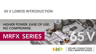
- 1. 65 V LDMOS INTRODUCTION
- 2. 1 Introduction • NXP is announcing a new LDMOS technology using 65 V drain voltage, focused on ease of use. − Higher voltage enables a higher RF output power with no compromise. • The first transistor of the 65 V MRFX series is the MRFX1K80, the industry’s most powerful CW RF transistor: 1800 W. • The MRFX1K80 is pin-compatible with existing 50 V transistors, to reduce design cycle times.
- 3. 2 A Brief History • 2006-2009: first to release a 1kW LDMOS transistor, followed by four other lower power devices. • 2010-2012: launched industry-first portfolio of 5 extremely rugged 50 V LDMOS transistors in ceramic packaging, from 25 to 1250 W. • 2014-2015: complemented this portfolio with 5 transistors in plastic package, enabling lower thermal resistance. • 2016: launched the 1500 W MRF1K50, pushing 50 V LDMOS close to its limits of usability (higher power levels at 50V are challenging to match to 50 ohm). • 2017: introducing the MRFX series with the 1800 W MRFX1K80, based on new 65 V LDMOS technology developed in NXP’s internal fab. Designed for ease of use.
- 4. 3 1. More power – Higher voltage enables higher power density, which helps reduce the number of transistors to combine. 2. Faster development time – With higher voltage, the output power can be increased while retaining a reasonable output impedance. 3. Design reuse – This impedance benefit also ensures pin-compatibility with current 50 V LDMOS transistors for better scalability. 4. Manageable current level – Higher voltage reduces the current losses in the system. 5. Wide safety margin – The higher breakdown voltage of 182 V improves ruggedness and allows for higher efficiency classes of operation. Why 65V? Ease of use. Fewer combining losses, smaller PAs, simpler power supply management. Easier matching to 50 ohms; transistors can be used wideband. Fewer stresses on DC supplies, better system efficiency, less magnetic radiation. Better reliability, higher efficiency. Little to no retuning from existing 50 V power amplifiers.
- 5. 4 NXP RF Technology Design Strategy: Focus on Ease of Use To keep a reasonable output impedance above 1500 W, NXP is raising the voltage Ease of use = higher power WITH higher voltage. RL = V2 2P Output impedance Higher impedance makes it easier to match to 50 ohm. Drain voltage NXP is raising the voltage V to increase the output power P, while keeping the output impedance RL reasonable. RL = (652 / 2x900W) x 2 sides = 4.7 ohm* (transformation ratio to 50 ohms = ~10) Output power. NXP’s competitors increase output power P while retaining V = 50 V. Consequence: reduced output resistance, making the transistors difficult to match and very challenging to use wideband. RL = (502 / 2x900W) x 2 sides = 2.8 ohm* (transformation ratio to 50 ohms = ~18) *: examples for a 1800W push-pull transistor.
- 6. 5 NXP RF Transistor Design Strategy: Focus on Scalability • Same PCB for MRFE6VP61K25H MRE6VP61K25N MRF1K50H MRF1K50N MRFX1K80H MRFX1K80N • Little to no retuning needed • Faster Time-To-Market • One platform, multiple products 1800 W 65 V 1500 W 50 V 1250 W 50 V Transistors from the MRFX series fit into existing PCBs designed for previous 50 V transistors
- 7. 6 0 10 20 30 40 50 60 70 80 90 0 200 400 600 800 1000 1200 1400 1600 1800 2000 Easy Upgrade from Existing 50 V Solutions 0 200 400 600 800 1000 1200 1400 1600 1800 2000 0.0 0.5 1.0 1.5 2.0 2.5 3.0 3.5 4.0 4.5 MRFE6VP61K25H 50 V MRFX1K80H @ 50 V MRFX1K80H @ 57.5 V MRFX1K80H @ 65 V Output power (W CW) Input power (W) MRFE6VP61K25H @ 50 V MRFX1K80H @ 50 V MRFX1K80H @ 57.5 V MRFX1K80H @ 65 V Efficiency (%) Output power (W) Data taken on the same 27 MHz reference circuit: no retuning
- 8. 7 MRFX1K80 Specifications • 1800 W CW • 1.8-470 MHz (unmatched input and output) • 65 V LDMOS for 30-65 V operations • 182 V min breakdown voltage V(BR)DSS • Extreme ruggedness: handles 65:1 VSWR • Warranted availability until 2032 minimum • MRFX1K80H: housed in NI-1230 air cavity ceramic package • Thermal resistance 0.09°C/W • Sampling now, production August 2017 • MRFX1K80N: housed in OM-1230 over-molded plastic package • Thermal resistance typically 30% lower than ceramic • Sampling August, production November 2017
- 9. 8 MRFX1K80H Reference Circuits Frequency Signal type Voltage Output Power Gain Drain efficiency Availability 27 MHz CW 50 V 1200 W 26.0 dB 82.3% Now57.5 V 1520 W 27.0 dB 80.1% 65 V 1800 W 27.8 dB 75.6% 87.5-108 MHz CW 60 V 1550 W 21.9 dB 82.2% Now 144 MHz CW 65 V 1800 W 23.5 dB 77.5% July 230 MHz Pulse 65 V 1800 W 24.0 dB 74.0% July
- 10. 9 MRFX1K80 Target Markets • Industrial, Scientific, Medical (ISM) − Laser generation − Plasma etching − Magnetic Resonance Imaging (MRI) − Diathermy, skin laser, RF ablation − Industrial heating, welding and drying systems − Particle accelerators • Broadcast − Radio broadcast (FM/DAB) − VHF TV broadcast • Aerospace − VHF omnidirectional range (VOR) − HF and VHF communications − Weather radar • Mobile Radio − VHF base stations
- 11. 10 For more information • 65 V LDMOS web page: www.nxp.com/65V • MRFX1K80H web page with datasheet: www.nxp.com/MRFX1K80H
- 12. 11 More power Faster development time Design reuse Lower current Wide safety margin Easy to use.