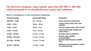
The microwave frequencyrange typically spans from 300 MHz to 300 GHz,
which corresponds to wavelengths between 1 meter and 1 millimeter.
Here's a breakdown of the microwave spectrum:
Frequency Range Wavelength Range Description
300 MHz – 1 GHz 1 m – 30 cm Lower microwave (UHF band)
1 GHz – 3 GHz 30 cm – 10 cm
L-band, used in radar, GPS, some
satellites
3 GHz – 6 GHz 10 cm – 5 cm S-band, weather radar, Wi-Fi (5 GHz)
6 GHz – 12 GHz 5 cm – 2.5 cm
C-band and X-band, satellite and
radar systems
12 GHz – 18 GHz 2.5 cm – 1.7 cm Ku-band, used in satellite TV
18 GHz – 26.5 GHz 1.7 cm – 1.1 cm
K-band, radar, satellite
communication
26.5 GHz – 40 GHz 1.1 cm – 7.5 mm Ka-band, high-frequency satellite
links
40 GHz – 300 GHz 7.5 mm – 1 mm
Millimeter wave (mmWave), used in
5G, advanced radar
3.
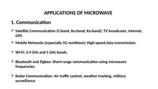
APPLICATIONS OF MICROWAVE
1.Communication
Satellite Communication (C-band, Ku-band, Ka-band): TV broadcasts, internet,
GPS.
Mobile Networks (especially 5G mmWave): High-speed data transmission.
Wi-Fi: 2.4 GHz and 5 GHz bands.
Bluetooth and Zigbee: Short-range communication using microwave
frequencies.
Radar Communication: Air traffic control, weather tracking, military
surveillance.
4.
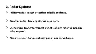
2. Radar Systems
Military radar: Target detection, missile guidance.
Weather radar: Tracking storms, rain, snow.
Speed guns: Law enforcement use of Doppler radar to measure
vehicle speed.
Airborne radar: For aircraft navigation and surveillance.
5.
3. Medical Applications
Deep tissue heating in physiotherapy.
Cancer treatment using localized microwave heating.
Imaging: Microwave imaging is under research for breast cancer and brain imaging.
4. Remote Sensing
Earth observation satellites: Measure soil moisture, ocean salinity, ice thickness.
Microwave radiometers: Measure natural microwave emissions from Earth.
6.
6. Industrial &Scientific
Material drying: Drying of ceramics, rubber, paper,
and textiles.
Microwave spectroscopy: Chemical analysis and
molecular structure detection.
7.
UNIT-1
Microwave Tubes
• Limitationsand Losses of conventional Tubes at Microwave
Frequencies
• Microwave Tubes – O Type and M Type Classifications
• Two Cavity Klystrons
• Reflex Klystrons
• Helix TWTs
8.
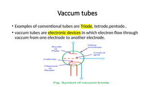
Vaccum tubes
• Examplesof conventional tubes are Triode, tetrode,pentode..
• vaccum tubes are electronic devices in which electron flow through
vaccum from one electrode to another electrode.
9.
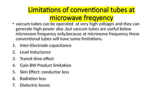
Limitations of conventionaltubes at
microwave freqyency
• vaccum tubes can be operated at very high voltages and they can
generate high power also ,but vaccum tubes are useful below
microwave frequency only,because at microwave frequency these
conventional tubes will have some limitations.
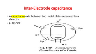
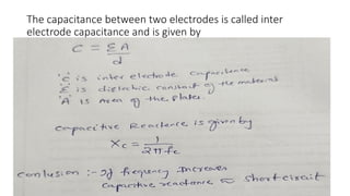
1. Inter-Electrode capacitance
2. Lead Inductance
3. Transit time effect
4. Gain BW Product limitation
5. Skin Effect: conductor loss
6. Radiation loss
7. Dielectric losses
• Grid-to-Plate (Cgp):This is the capacitance between the grid and the
plate (anode). It's often the largest of the interelectrode capacitances
because of the larger plate area.
• Grid-to-Cathode (Cgk): This is the capacitance between the grid and
the cathode.
• Plate-to-Cathode (Cpk): This is the capacitance between the plate and
the cathode
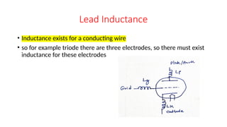
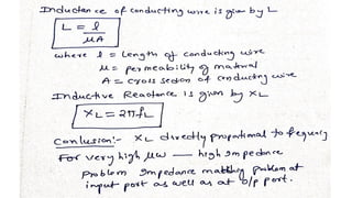
Lead Inductance
• Inductanceexists for a conducting wire
• so for example triode there are three electrodes, so there must exist
inductance for these electrodes
15.
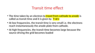
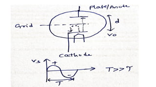
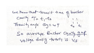
Transit time effect
•The time taken by an electron to travel from cathode to anode is
called as transit time and it is given by T=d/v
• At low frequencies, the transit time is very small i.e. the electrons
reach instantaneously the anode plate from cathode.
• At high frequencies, the transit time becomes large because the
source driving the grid becomes loaded
17.
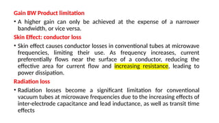
Gain BW Productlimitation
• A higher gain can only be achieved at the expense of a narrower
bandwidth, or vice versa.
Skin Effect: conductor loss
• Skin effect causes conductor losses in conventional tubes at microwave
frequencies, limiting their use. As frequency increases, current
preferentially flows near the surface of a conductor, reducing the
effective area for current flow and increasing resistance, leading to
power dissipation.
Radiation loss
• Radiation losses become a significant limitation for conventional
vacuum tubes at microwave frequencies due to the increasing effects of
inter-electrode capacitance and lead inductance, as well as transit time
effects
18.
Dielectric losses
• Dielectriclosses are a significant limitation for conventional tubes at
microwave frequencies because the loss tangent of a dielectric
material increases with frequency. This means that the energy
absorbed by the dielectric materials used in the tube, like
encapsulating materials, increases with frequency, resulting in higher
power dissipation and reduced efficiency.
• Dielectric losses are more at microwave frequency.
19.
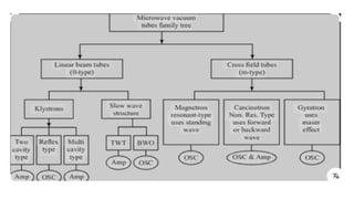
Types of MicrowaveTubes
• Microwave tubes are categorized into two main types: linear beam
tubes (O-type) and crossed-field tubes (M-type)
• Linear beam tubes, like klystrons and traveling wave tubes (TWTs), use
an electron beam traveling along the same direction as the magnetic
field.
• Crossed-field tubes, like magnetrons, utilize an electron beam and
magnetic field perpendicular to each other.
20.
Linear Beam Tubes(O-type):
Klystron:
• A microwave tube that uses velocity modulation to amplify or generate microwave signals.
1.Two-cavity Klystron: A common type used as an amplifier in radar and communication
systems.
2.Reflex Klystron: A type used for generating microwave signals at a specific frequency, with
fine tuning via the repeller voltage.
Traveling Wave Tube (TWT):
• A microwave amplifier known for its wide bandwidth, used in communication and radar
applications.
1.Helix TWT: A specific type of TWT using a helix structure for slow-wave interaction.
2.Backward-wave Oscillator (BWO):
A type of TWT used for generating microwaves up to the terahertz range, offering a wide
electronic tuning range
21.
M-type microwave tubesclassification
• M-type microwave tubes, also known as crossed-field tubes,
are classified into resonant and non-resonant types based on
their operating principle and structure.
• Resonant M-type tubes, like magnetrons, utilize resonant
cavities for oscillations, while non-resonant types, like the
relativistic magnetron, operate without resonant cavities.
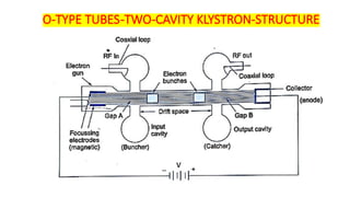
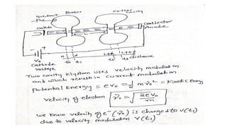
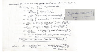
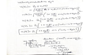
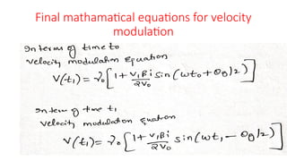
Two-Cavity Klystron-Velocity modulationprocess
• Electrons Emitted from the cathode will reach to first cavity with
uniform velocity.
• In first cavity the velocity of these electrons will be modulated by the
input RF Signal present there in first cavity and this is called as velocity
modulation.
• Because of velocity modulation electrons form bunches as they drift
down the tube and that is called as bunch formation.
• Beacuse of this bunch formation , the density of the electron in the
catcher cavity varies periodically with time that means the electron
beam contains AC component of the current that is known as current
modulation.
• At Second cavity all the energy comes out and final amplifed signal is
produced using Two cavity klystron.
25.
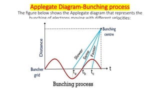
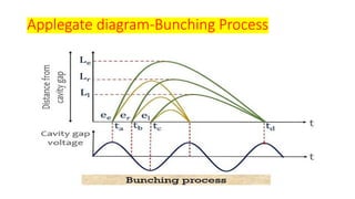
Applegate Diagram-Bunching process
Thefigure below shows the Applegate diagram that represents the
bunching of electrons moving with different velocities:
26.
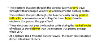
• The electronsthat pass through the buncher cavity at Vs=0 travel
through with unchanged velocity Vo and become the buching center.
• The electrons that pass through , the buncher cavity during positive
half cycles of microwave input voltage Vs travel faster than the
electrons that passed the gap at Vs=0
• Those electrons that pass the buncher cavity during the -ve half cycles
of voltage Vs travel slower than the electrons that passed the gap
when VS=0
• At a distance DEL L from the buncher cavity , the beam electrons have
drifted into dense clusters.
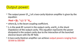
Output power:
• Theoutput power (Pout) of a two-cavity klystron amplifier is given by the
equation:
Pout = (β₀ * I₂) / 2 * Rsh,
• where β₀ is the beam coupling coefficient,
• I₂ is the peak RF current in the output cavity, and Rsh is the shunt
impedance of the output cavity. This equation represents the power
dissipated in the output cavity due to the interaction of the bunched
electron beam with the RF field.
• A two-cavity klystron amplifier can achieve output powers ranging from
10 kW to 500 kW
34.
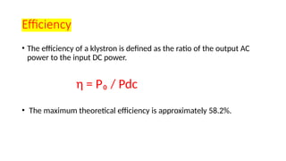
Efficiency
• The efficiencyof a klystron is defined as the ratio of the output AC
power to the input DC power.
η = P₀ / Pdc
• The maximum theoretical efficiency is approximately 58.2%.
35.
small signal theoryfor two cavity klystron
• Small signal theory for a two-cavity klystron analyzes the device's
behavior when subjected to a small input signal. It focuses on how
the input signal modulates the electron beam's velocity (velocity
modulation), leading to bunching and, ultimately, amplification of the
signal in the output cavity. This theory helps predict and optimize the
klystron's performance, such as gain and efficiency, under these
specific conditions.
36.
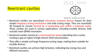
Reentrant cavities
• Reentrantcavities are specialized microwave resonant devices known for their
simple frequency tuning mechanism and wide tuning range. They are essentially
3D lumped LC circuits formed by a conducting post within a resonant cavity.
These cavities are used in various applications, including tunable devices, bulk
acoustic wave (BAW) resonators.
• Reentrant cavities consist of a central post (or posts) extending into a cavity,
creating a gap or region of high electric field concentration.
• They offer a simple and large frequency tuning range, making them suitable for
tunable devices.
• Reentrant cavities can achieve high Q-factors, indicating low energy loss and
efficient resonance.
37.
Applications
• The two-cavityKlystron finds application in satellite communication,
UHF TV transmitters as well as radar systems, wideband high power
communication and troposphere scatter transmitters etc.
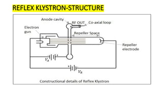
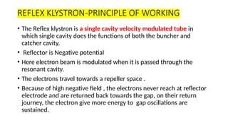
REFLEX KLYSTRON-PRINCIPLE OFWORKING
• The Reflex klystron is a single cavity velocity modulated tube in
which single cavity does the functions of both the buncher and
catcher cavity.
• Reflector is Negative potential
• Here electron beam is modulated when it is passed through the
resonant cavity.
• The electrons travel towards a repeller space .
• Because of high negative field , the electrons never reach at reflector
electrode and are returned back towards the gap, on their return
journey, the electron give more energy to gap oscillations are
sustained.
40.
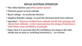
REFLEX KLYSTRON OPERATION
•The reflex klystron uses three power sources
• Filament power-to heat cathode
• Beam voltage - to accelerate electron
• Negative Repeller voltage- to push the electrons back from reflector
• operation :- Electrons emitted from cathode travels from grid gap and
relects from reflector , in the return journey the energy of electrons is
more these cause oscillations at grid gap.
• Note: Here it is assumed that the oscillations are setup in the tube
intially due to noise or switching transientsi.e.., vs=v1sinwt
41.
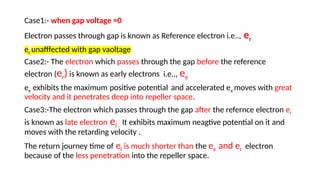
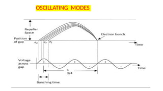
Case1:- when gapvoltage =0
Electron passes through gap is known as Reference electron i.e.., er
er unafffected with gap vaoltage
Case2:- The electron which passes through the gap before the reference
electron (er) is known as early electrons i.e.., ee
ee exhibits the maximum positive potential and accelerated ee moves with great
velocity and it penetrates deep into repeller space.
Case3:-The electron which passes through the gap after the refernce electron er
is known as late electron el . It exhibits maximum neagtive potential on it and
moves with the retarding velocity .
The return journey time of el is much shorter than the ee and er electron
because of the less penetration into the repeller space.
42.
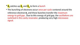
•el catches uper and ee to form a bunch
• The bunching of electrons occur once per cycle centered around the
reference electron er and these bunches transfer the maximum
energy to grid gap . Due to this energy of grid gap, the oscillations are
switched in the cavity resonator, producing very high microwave
signal.
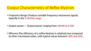
Output Characteristics ofReflex Klystron
• Frequency Range: Produce variable frequency microwave signals,
typically in the 1-20 GHz range
• Output power :- Output power ranging from 10mW to 2.5W.
• Efficency:The efficiency of a reflex klystron is relatively low compared
to other microwave tubes, with typical values between 10% and 20%.
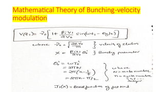
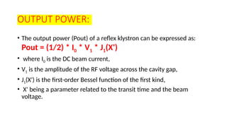
OUTPUT POWER:
• Theoutput power (Pout) of a reflex klystron can be expressed as:
Pout = (1/2) * I0 * V1 * J1(X')
• where I0 is the DC beam current,
• V1 is the amplitude of the RF voltage across the cavity gap,
• J1(X') is the first-order Bessel function of the first kind,
• X' being a parameter related to the transit time and the beam
voltage.
48.
Efficiency :
• EfficiencyDefinition:
• Efficiency (η) is defined as the ratio of the output AC power (Pac) to
the input DC power (Pdc) of the reflex klystron.
η = [2 * x' * J1(x')] / (2πn - π/2)
• where 'x' is a dimensionless parameter related to the bunching of
electrons
• J1 is the first-order Bessel function, and 'n' is the mode number
representing the number of cycles the electron takes to return to the
cavity.
49.
Applications of ReflexKlystron-oscillator
• Reflex Klystron is used in applications where variable frequency is
desirable, such as −
• Radio receivers
• Portable microwave links
• Local oscillators of microwave receivers
• As a signal source where variable frequency is desirable in microwave
generators.
50.
Slow-Wave Structures (SWS)
•Slow-Wave Structures (SWS)
• In microwave engineering and vacuum electronics, a Slow-Wave
Structure (SWS) is engineered transmission line that slows down the
phase velocity of an electromagnetic wave so it can interact continuously
with a traveling electron beam.
• Electromagnetic waves in free space travel at the speed of light
• Electron beams typically move at a much slower velocity.
• For efficient interaction (like amplification or oscillation), the wave and
electron beam must travel at similar speeds.
• SWS reduces the phase velocity of the wave to match that of the electron
beam.
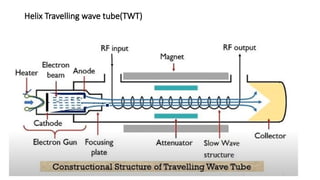
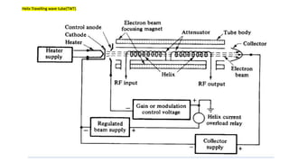
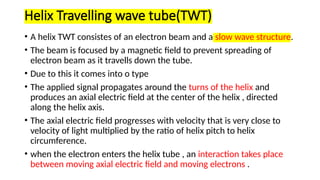
Helix Travelling wavetube(TWT)
• A helix TWT consistes of an electron beam and a slow wave structure.
• The beam is focused by a magnetic field to prevent spreading of
electron beam as it travells down the tube.
• Due to this it comes into o type
• The applied signal propagates around the turns of the helix and
produces an axial electric field at the center of the helix , directed
along the helix axis.
• The axial electric field progresses with velocity that is very close to
velocity of light multiplied by the ratio of helix pitch to helix
circumference.
• when the electron enters the helix tube , an interaction takes place
between moving axial electric field and moving electrons .
54.
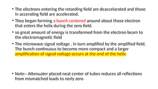
• The electronsentering the retarding field are deaccelarated and those
in accerating field are accelerated.
• They began forming a bunch centered around about those electron
that enters the helix during the zero field.
• so great amount of energy is transformed from the electron beam to
the electromagnetic field
• The microwave signal voltage , in turn amplified by the amplified field.
The bunch continuous to become more compact and a larger
amplification of signal voltage occurs at the end of the helix
• Note:- Attenuater placed neat center of tubes reduces all reflections
from mismatched loads to nerly zero
55.
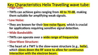
Key Characteristics HelixTravelling wave tube:
• High Gain:
• TWTs can achieve gains ranging from 40 to 70 dB, making
them suitable for amplifying weak signals.
• Low Noise:
• They are known for their low noise figure, which is crucial
for applications requiring sensitive signal detection.
• Wide Bandwidth:
• TWTs can operate over a wide range of frequencies
• Slow-Wave Structure:
• The heart of a TWT is the slow-wave structure (e.g., helix),
which slows down the RF wave to allow for continuous
interaction with the electron beam.
56.
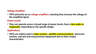
Voltage Amplifier:
• TWTsprimarily act as voltage amplifiers, meaning they increase the voltage of
the amplified signal.
Power Levels:
• They can operate across a broad range of power levels, from a few watts to
megawatts, depending on the specific design.
Applications:
• TWTs are widely used in radar systems, satellite communications, electronic
warfare, and test and measurement equipment due to their unique
characteristics.


![Efficiency :
• Efficiency Definition:
• Efficiency (η) is defined as the ratio of the output AC power (Pac) to
the input DC power (Pdc) of the reflex klystron.
η = [2 * x' * J1(x')] / (2πn - π/2)
• where 'x' is a dimensionless parameter related to the bunching of
electrons
• J1 is the first-order Bessel function, and 'n' is the mode number
representing the number of cycles the electron takes to return to the
cavity.](https://image.slidesharecdn.com/mwocunit-1ppt-microwavetubes-250710050809-42932188/85/MW-OC-UNIT-1-PPT-MICROWAVE-TUBES-pptx-INTRODUCTION-48-320.jpg)