Modeling of power electronics converters 2
•
1 like•698 views

Small signal modeling of DC-DC converters is discussed.Need for controller is also discussed

Recommended
More Related Content
What's hot
What's hot (20)
Similar to Modeling of power electronics converters 2
Similar to Modeling of power electronics converters 2 (20)
Recently uploaded
Recently uploaded (20)
Modeling of power electronics converters 2
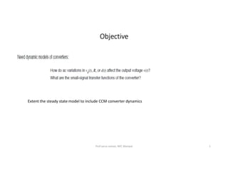
- 1. ObjectiveObjectiveObjectiveObjective Extent the steady state model to include CCM converter dynamics Prof:sarun soman, MIT, Manipal 1
- 2. Modeling ApproachModeling ApproachModeling ApproachModeling Approach Prof:sarun soman, MIT, Manipal 2
- 3. Response to AC variationsResponse to AC variationsResponse to AC variationsResponse to AC variations Prof:sarun soman, MIT, Manipal 3
- 4. Output Voltage SpectrumOutput Voltage SpectrumOutput Voltage SpectrumOutput Voltage Spectrum Prof:sarun soman, MIT, Manipal 4
- 5. Objective of ac converter modelingObjective of ac converter modelingObjective of ac converter modelingObjective of ac converter modeling Prof:sarun soman, MIT, Manipal 5
- 6. Averaging to remove switching rippleAveraging to remove switching rippleAveraging to remove switching rippleAveraging to remove switching ripple Moving average Prof:sarun soman, MIT, Manipal 6
- 7. Non-linear averaged equations Prof:sarun soman, MIT, Manipal 7
- 8. Small Signal modeling of diode Prof:sarun soman, MIT, Manipal 8
- 9. Buck-Boost Converter Prof:sarun soman, MIT, Manipal 9
- 10. Basic ac modeling approachBasic ac modeling approachBasic ac modeling approachBasic ac modeling approach Prof:sarun soman, MIT, Manipal 10
- 11. Switch in position 1 Prof:sarun soman, MIT, Manipal 11
- 12. Switch in position 2 Prof:sarun soman, MIT, Manipal 12
- 13. Averaging the InductorAveraging the InductorAveraging the InductorAveraging the Inductor WWWWaveformsaveformsaveformsaveforms Prof:sarun soman, MIT, Manipal 13
- 14. Averaging the Capacitor WaveformsAveraging the Capacitor WaveformsAveraging the Capacitor WaveformsAveraging the Capacitor Waveforms Prof:sarun soman, MIT, Manipal 14
- 15. Averaging Input Current WaveformAveraging Input Current WaveformAveraging Input Current WaveformAveraging Input Current Waveform Prof:sarun soman, MIT, Manipal 15
- 16. Perturbation and linearization Prof:sarun soman, MIT, Manipal 16
- 17. Perturbation Prof:sarun soman, MIT, Manipal 17
- 18. Small Signal assumption Prof:sarun soman, MIT, Manipal 18
- 19. Perturbation of Inductor EquationPerturbation of Inductor EquationPerturbation of Inductor EquationPerturbation of Inductor Equation ܮ ݀ I ଓ̂ ݐ ݀ݐ ൌ ܸܦ ܸ′ܦ ௧ ݒܦො ݐ ݒ′ܦො ݐ ሺܸ െ ܸሻ݀መ ݐ ி௦௧ ௗ ୟୡ ௧௦ ሺሻ ݀መ ݐ ݒො ݐ െ ݀መ ݐ ݒො ݐ ௦ௗ ௗ ௧ ሺିሻ Prof:sarun soman, MIT, Manipal 19
- 20. The Perturbed Inductor EquationThe Perturbed Inductor EquationThe Perturbed Inductor EquationThe Perturbed Inductor Equation ܮ ݀ ଓ̂ ݐ ݀ݐ ൌ ܸܦ ܸ′ܦ ௧ ݒܦො ݐ ݒ′ܦො ݐ ሺܸ െ ܸሻ݀መ ݐ ி௦௧ ௗ ୟୡ ௧ ݀መ ݐ ݒො ݐ െ ݀መ ݐ ݒො ݐ ௦ௗ ௗ ௧ Prof:sarun soman, MIT, Manipal 20
- 21. Linearized Inductor Equation Prof:sarun soman, MIT, Manipal 21
- 22. Capacitor EquationCapacitor EquationCapacitor EquationCapacitor Equation ܥ ݀ሺܸ ݒො ݐ ሻ ݀ݐ ൌ Prof:sarun soman, MIT, Manipal 22
- 23. Capacitor EquationCapacitor EquationCapacitor EquationCapacitor Equation Prof:sarun soman, MIT, Manipal 23
- 24. Average Input CurrentAverage Input CurrentAverage Input CurrentAverage Input Current Prof:sarun soman, MIT, Manipal 24
- 25. Construction of small signal equivalent circuit modelConstruction of small signal equivalent circuit modelConstruction of small signal equivalent circuit modelConstruction of small signal equivalent circuit model Prof:sarun soman, MIT, Manipal 25
- 26. Inductor loop equation Prof:sarun soman, MIT, Manipal 26
- 27. Capacitor node equationCapacitor node equationCapacitor node equationCapacitor node equation Prof:sarun soman, MIT, Manipal 27
- 28. Input port node equationInput port node equationInput port node equationInput port node equation Prof:sarun soman, MIT, Manipal 28
- 29. Complete Equivalent circuitComplete Equivalent circuitComplete Equivalent circuitComplete Equivalent circuit Prof:sarun soman, MIT, Manipal 29
- 30. Small signal model of Buck and BoostSmall signal model of Buck and BoostSmall signal model of Buck and BoostSmall signal model of Buck and Boost Prof:sarun soman, MIT, Manipal 30
- 31. Modeling the pulse width modulatorModeling the pulse width modulatorModeling the pulse width modulatorModeling the pulse width modulator Prof:sarun soman, MIT, Manipal 31
- 32. Simple pulse width modulatorSimple pulse width modulatorSimple pulse width modulatorSimple pulse width modulator Prof:sarun soman, MIT, Manipal 32
- 33. Equation of pulse width modulatorEquation of pulse width modulatorEquation of pulse width modulatorEquation of pulse width modulator Prof:sarun soman, MIT, Manipal 33
- 34. Perturbed equation of pulse width modulator Prof:sarun soman, MIT, Manipal 34
- 35. Canonical circuit modelCanonical circuit modelCanonical circuit modelCanonical circuit model Prof:sarun soman, MIT, Manipal 35
- 36. Development of Canonical circuit model Prof:sarun soman, MIT, Manipal 36
- 37. Development of Canonical circuit modelDevelopment of Canonical circuit modelDevelopment of Canonical circuit modelDevelopment of Canonical circuit model Prof:sarun soman, MIT, Manipal 37
- 38. Development of Canonical circuit modelDevelopment of Canonical circuit modelDevelopment of Canonical circuit modelDevelopment of Canonical circuit model Prof:sarun soman, MIT, Manipal 38
- 39. Development of Canonical circuit modelDevelopment of Canonical circuit modelDevelopment of Canonical circuit modelDevelopment of Canonical circuit model Prof:sarun soman, MIT, Manipal 39
- 40. Transfer functions predicted by canonical modelTransfer functions predicted by canonical modelTransfer functions predicted by canonical modelTransfer functions predicted by canonical model Prof:sarun soman, MIT, Manipal 40
- 41. Manipulation of Buck Boost converter model into canonical formManipulation of Buck Boost converter model into canonical formManipulation of Buck Boost converter model into canonical formManipulation of Buck Boost converter model into canonical form Prof:sarun soman, MIT, Manipal 41
- 42. Step 1 Prof:sarun soman, MIT, Manipal 42
- 43. Step 2 Prof:sarun soman, MIT, Manipal 43
- 44. Step 3 Prof:sarun soman, MIT, Manipal 44
- 45. Step 4 Prof:sarun soman, MIT, Manipal 45
- 46. Canonical model of Buck-Boost Converter Prof:sarun soman, MIT, Manipal 46
- 47. Voltage source coefficient e(s) ݁ሺݏሻ = ି െ ௦ூ ᇲ (1) ݁ ݏ ൌ ି ௦ ሺᇲሻమோ Inductor current and output current relation ܦᇱܫ ൌ െ ோ Substitute in (1) ൌ െ 1 ௦ ሺᇲሻమோ ൌ െ ᇲ െ 1 ௦ ሺᇲሻమோ ൌ െ ଵ ௦ ሺᇲሻమோ ݁ ݏ ൌ െ మ 1 െ ௦ ሺᇲሻమோ Prof:sarun soman, MIT, Manipal 47
- 48. Canonical Circuit Parameters for Some Common converters Prof:sarun soman, MIT, Manipal 48
- 49. Buck Converter Small Signal model Switch ON Inductor Voltage ݒ ݐ ൌ ܮ ௗ ௗ௧ ൌ ݒ ݐ െ ݒሺݐሻ Capacitor Current ݅ ݐ ൌ ܥ ௗ௩ሺ௧ሻ ௗ௧ ൌ ݅ሺݐሻ െ ௩ሺ௧ሻ ோ By small ripple approximation ݒ ݐ ൌ ܮ ݀݅ ݐ ݀ݐ ൌ < ݒ ݐ >்ೞ െ < ݒሺݐሻ >்ೞ ݅ ݐ ൌ ܥ ௗ௩ሺ௧ሻ ௗ௧ ൌ< ݅ሺݐሻ >்ೞ െ ழ௩ሺ௧ሻவೞ ோ Prof:sarun soman, MIT, Manipal 49
- 50. Switch ‘off’ ݒ ݐ ൌ െݒሺݐሻ ݅ ݐ ൌ < ݅ ݐ >்ೞ െ ழ௩ሺ௧ሻவೞ ோ By small ripple approximation ݒ ݐ ൌ ܮ ݀݅ ݐ ݀ݐ ൌ െ < ݒሺݐሻ >்ೞ ݅ ݐ ൌ ܥ ௗ௩ሺ௧ሻ ௗ௧ ൌ < ݅ ݐ >்ೞ െ ழ௩ሺ௧ሻவೞ ோ Averaging inductor voltage and capacitor voltage ܮ ௗழಽሺ௧ሻவೞ ௗ௧ ൌ ݀ ݐ < ݒ ݐ >்ೞ െ ݀ᇱ ݐ < ݒ ݐ >்ೞ ܥ ௗழ௩ሺ௧ሻவೞ ௗ௧ ൌ < ݅ ݐ >்ೞ െ ழ௩ ௧ வೞ ோ Prof:sarun soman, MIT, Manipal 50
- 51. Source current Source Current < ݅ >்ೞ ൌ ݀ ݐ < ݅ ݐ >்ೞ Prof:sarun soman, MIT, Manipal 51
- 52. Perturbation Applying < ݒ ݐ >்ೞ ൌ ܸ ݒොሺݐሻ and ݀ ݐ ൌ ܦ ݀መሺݐሻ as input which results in < ݅ ݐ >்ೞ ൌ I ଓ̂ ݐ < ݒ ݐ >்ೞ ൌ ܸ ݒොሺݐሻ The two equations are non-linear, which can be linearized by assuming ݒො ݐ ≪ ܸ, ݒො ݐ ≪ ܸ, ଓ̂ ݐ ≪ I, ݀መ ݐ ≪ ܦ Prof:sarun soman, MIT, Manipal 52
- 53. Perturbed Inductor loop equation ܮ ௗሺ ୍ಽା ప̂ಽ ௧ ሻ ௗ௧ ൌ ܦ ݀መ ݐ ܸ ݒො ݐ െ ܸ െ ݒොሺݐሻ ܦᇱ െ ݀መ ݐ െܸ െ ݒො ݐ ܮ ݀ ଓ̂ ݐ ݀ݐ ൌ ܸܦ െ ܸ′ܦ െ ܸܦ ௧ ݒܦො ݐ ݀መ ݐ ܸ െ ݒොሺݐ൯ ி௦௧ ௗ ௧ ݀መ ݐ ݒො ݐ ݀መ ݐ ݒො ݐ െ ݀መ ݐ ݒො ݐ ௦ௗ ௗ ௧ DC term is zero and second order term can neglected due to smaller magnitude ܮ ௗ ప̂ಽ ௧ ௗ௧ ൌ ݀መ ݐ ܸ ݒܦො ݐ െ ݒොሺݐሻ Prof:sarun soman, MIT, Manipal 53
- 54. Perturbed Capacitor Current ܥ ௗሺା௩ො ௧ ሻ ௗ௧ ൌ ܫ ଓ̂ ݐ െ ோ െ ௩ො ௧ ோ DC term is zero and neglecting the second order term gives the equation ܥ ௗ௩ො ௧ ௗ௧ ൌ ଓ̂ ݐ െ ௩ො ௧ ோ Perturbing the source current ܫ ଓ̂ ݐ ൌ ሺܦ ݀መሺݐሻሻሺܫ ଓ̂ሺݐሻሻ Neglecting the DC term ଓ̂ ݐ ൌ ܦଓ̂ ݐ ݀መ ݐ ܫ Prof:sarun soman, MIT, Manipal 54
- 55. Small Signal model Inductor Loop Equation ܮ ௗ ప̂ಽ ௧ ௗ௧ ൌ ݀መ ݐ ܸ ݒܦො ݐ െ ݒොሺݐሻ Prof:sarun soman, MIT, Manipal 55
- 56. Capacitor Current Equation ܥ ݀ݒො ݐ ݀ݐ ൌ ଓ̂ ݐ െ ݒො ݐ ܴ Prof:sarun soman, MIT, Manipal 56
- 57. Input Port model ଓ̂ ݐ ൌ ܦଓ̂ ݐ ݀መ ݐ ܫ ܦଓ̂ ݐ݀መ ݐ ܫ ݒො ݐ Prof:sarun soman, MIT, Manipal 57
- 58. Complete modelComplete modelComplete modelComplete model ܦଓ̂ ݐ݀መ ݐ ܫݒො ݐ ݒො ݐ ݀መ ݐ ܫ ܮ ݀ ଓ̂ ݐ ݀ݐ ܥ ݀ݒො ݐ ݀ݐ ݒොሺݐ 1: ܦ ܴ ݀መ ݐ ܸ Prof:sarun soman, MIT, Manipal 58
- 59. Buck Converter Canonical ModelBuck Converter Canonical ModelBuck Converter Canonical ModelBuck Converter Canonical Model ݒොሺݏሻ ݒො ݏ ܸ ܴ ݀መ ݏ sܮ 1 ܥݏ 1: ܦ ܴ ܸ ܦଶ ݀መ ݏ Prof:sarun soman, MIT, Manipal 59
- 60. Transfer FunctionTransfer FunctionTransfer FunctionTransfer Function BUCK BOOST Converter Canonical model Prof:sarun soman, MIT, Manipal 60
- 61. Line to output transferLine to output transferLine to output transferLine to output transfer functionfunctionfunctionfunction ܩ௩ ݏ |ௗ ௦ ୀ Applying voltage divider rule ݒො ݏ ൌ െ ᇲ ݒොሺݏሻ ோ// భ ೞ ೞಽ ሺವᇲሻమ ା ሺோ// భ ೞ ሻ ܩ௩ ݏ ൌ ௩ො ௦ ௩ොሺ௦ሻ ൌ െ ᇲ ோ/ଵା௦ோ ೞಽ ሺವᇲሻమ ା ሺோ/ଵା௦ோሻ ൌ െ ᇱ ோ ோା ೞಽ ሺವᇲሻమା ೞమೃಽ ሺವᇲሻమ Normalized form ܩ௩ ݏ ൌ െ ᇲ ଵ ଵା ೞಽ ವᇲೃ ା ೞమಽ ሺವᇲሻమ Prof:sarun soman, MIT, Manipal 61
- 62. Control to output transferControl to output transferControl to output transferControl to output transfer functionfunctionfunctionfunction ܩ௩ௗ ݏ |௩ොሺ௦ሻୀ ݒො ݏ ൌ െ ᇲ ݁ሺݏሻ݀መሺݏሻ ோ// భ ೞ ೞಽ ሺವᇲሻమ ା ሺோ// భ ೞ ሻ ݁ ݏ ൌ െ మ 1 െ ௦ ሺᇲሻమோ ܩ௩ௗ ݏ ൌ ௩ොሺ௦ሻ ௗሺ௦ሻ ൌ െ ᇲ ∗ െ మ 1 െ ௦ ሺᇲሻమோ ଵ ଵା ೞಽ ವᇲೃ ା ೞమಽ ሺವᇲሻమ ܩ௩ௗ ݏ ൌ ᇱ ଵି ೞಽವ ሺವᇲሻమೃ ଵା ೞಽ ವᇲೃ ା ೞమಽ ሺವᇲሻమ Prof:sarun soman, MIT, Manipal 62
- 63. Control to output transfer functionControl to output transfer functionControl to output transfer functionControl to output transfer function Comparing with standard normalized form ܩ௩ௗ ݏ ൌ ܩௗ ଵ ି ೞ ⍵⁄ ଵା ೄ ೂ⍵బ ା ሺ ೞ ⍵బ ሻమ ܩௗ ൌ ܸ ′ܦܦ ⍵௭ ൌ ሺᇲሻమோ ܳ ൌ ܴ′ܦ ⍵ ൌ ᇲ Prof:sarun soman, MIT, Manipal 63
- 64. RHP Zero effectRHP Zero effectRHP Zero effectRHP Zero effect Prof:sarun soman, MIT, Manipal 64
- 65. Line to output transferLine to output transferLine to output transferLine to output transfer functionfunctionfunctionfunction ܩ௩ ݏ ൌ ݒො ݏ ݒො ݏ |ௗ ௦ ୀ ݒො ݏ ൌ ݀መ ݏ ோ// భ ೞ ௦ାோ∕∕ భ ೞ ܩ௩ ݏ ൌ ௩ො ௦ ௗ ௦ ൌ ܦ ோ ௦ ା ௦మோାோ ܩ௩ ݏ ൌ ܦ ଵ ଵା௦ ಽ ೃ ା ௦మ Prof:sarun soman, MIT, Manipal 65
- 66. Control to output transferControl to output transferControl to output transferControl to output transfer functionfunctionfunctionfunction ܩ௩ௗ ݏ ൌ ݒො ݏ ݀መ ݏ |௩ො ௦ ୀ ݒො ݏ ൌ ݀መሺݏሻ ோ// భ ೞ ௦ାோ∕∕ భ ೞ ܩ௩ௗ ݏ ൌ ௩ො ௦ ௗ ௦ ൌ ଵ ଵା௦ ಽ ೃ ା ௦మ ܩௗ ൌ ⍵ ൌ ଵ ܳ ൌ ܴ Prof:sarun soman, MIT, Manipal 66
- 67. Controller DesignController DesignController DesignController Design 67 DC-regulator application Prof:sarun soman, MIT, Manipal
- 68. DC-regulator application 68Prof:sarun soman, MIT, Manipal
- 69. Negative feedback 69Prof:sarun soman, MIT, Manipal
- 70. Effect of negative feedback on the network transfer functions 70Prof:sarun soman, MIT, Manipal
- 71. Voltage Regulator System small signal modelVoltage Regulator System small signal modelVoltage Regulator System small signal modelVoltage Regulator System small signal model Prof:sarun soman, MIT, Manipal 71
- 72. Regulator system small signal block diagramRegulator system small signal block diagramRegulator system small signal block diagramRegulator system small signal block diagram ݒො ݏ ൌ ܩ௩ ݏ ݒො ݏ ܩ௩ௗ ݏ ݀መ ݏ െ ݖ௨௧ሺݏሻ݅ௗሺݏሻ Prof:sarun soman, MIT, Manipal 72
- 73. Solution of block diagramSolution of block diagramSolution of block diagramSolution of block diagram ݒො ݏ ൌ ݒො ݏ െ ܪሺݏሻݒොሺݏሻ (1) ݀መ ݏ ൌ ௩ො ௦ ீሺ௦ሻ ಾ (2) ݒො ݏ ൌ ܩ௩ ݏ ݒො ݏ ܩ௩ௗ ݏ ݀መ ݏ െ ݖ௨௧ሺݏሻ݅ௗሺݏሻ (3) Substitute (2) in (3) ݒො ݏ ൌ ܩ௩ ݏ ݒො ݏ െ ݖ௨௧ ݏ ଓ̂ௗ ݏ ܩ௩ௗ ݏ ௩ො ௦ ீሺ௦ሻ ಾ (4) Substitute (1) in (4) ݒො ݏ ൌ ܩ௩ ݏ ݒො ݏ െ ݖ௨௧ ݏ ଓ̂ௗ ݏ ܩ௩ௗ ݏ ܩ ݏ ݒො ݏ െ ܪ ݏ ݒො ݏ ܸெ Prof:sarun soman, MIT, Manipal 73
- 74. Solution of block diagramSolution of block diagramSolution of block diagramSolution of block diagram ݒො ݏ ൌ ܩ௩ ݏ ݒො ݏ െ ݖ௨௧ ݏ ݅ௗ ݏ ܩ௩ௗ ݏ ܩ ݏ ݒො ݏ ܸெ െ ܩ௩ௗ ݏ ܩ ݏ ܪ ݏ ݒො ݏ ܸெ ݒො ݏ 1 ீೡ ௦ ீ ௦ ு ௦ ಾ ൌ ܩ௩ ݏ ݒො ݏ െ ݖ௨௧ ݏ ଓ̂ௗ ݏ ܩ௩ௗ ݏ ீ ௦ ௩ොೝ ௦ ಾ Let ܶሺݏሻ ൌ ீೡ ௦ ீ ௦ ு ௦ ಾ loop gain ݒො ݏ ൌ ீೡ ௦ ଵା்ሺ௦ሻ ݒො ݏ ݒො ݏ ଵ ு ்ሺ௦ሻ ଵା்ሺ௦ሻ െ ௭ೠ ௦ ଵା்ሺ௦ሻ ଓ̂ௗ ݏ Prof:sarun soman, MIT, Manipal 74
- 75. Feed back reduces the transfer function from disturbances to outputFeed back reduces the transfer function from disturbances to outputFeed back reduces the transfer function from disturbances to outputFeed back reduces the transfer function from disturbances to output Prof:sarun soman, MIT, Manipal 75
- 76. Closed loop output impedanceClosed loop output impedanceClosed loop output impedanceClosed loop output impedance Prof:sarun soman, MIT, Manipal 76
- 77. Prof:sarun soman, MIT, Manipal 77
- 78. 1 1 ܶൗ 78Prof:sarun soman, MIT, Manipal
- 79. ܶ 1 ܶൗ 79Prof:sarun soman, MIT, Manipal
- 80. Regulator DesignRegulator DesignRegulator DesignRegulator Design Prof:sarun soman, MIT, Manipal 80
- 81. Relation b/w phase margin & closedRelation b/w phase margin & closedRelation b/w phase margin & closedRelation b/w phase margin & closed----loop damping factorloop damping factorloop damping factorloop damping factor Prof:sarun soman, MIT, Manipal 81
- 82. LowLowLowLow ----Q caseQ caseQ caseQ case Prof:sarun soman, MIT, Manipal 82
- 83. HighHighHighHigh----Q caseQ caseQ caseQ case Prof:sarun soman, MIT, Manipal 83
- 84. Q vs ɸ 84Prof:sarun soman, MIT, Manipal
- 85. Transient response vs damping factor 85Prof:sarun soman, MIT, Manipal
- 86. Lead CompensatorLead CompensatorLead CompensatorLead Compensator Prof:sarun soman, MIT, Manipal 86
- 87. Lead Compensator DesignLead Compensator DesignLead Compensator DesignLead Compensator Design Prof:sarun soman, MIT, Manipal 87
- 88. Lag Compensation(PI)Lag Compensation(PI)Lag Compensation(PI)Lag Compensation(PI) Prof:sarun soman, MIT, Manipal 88
- 89. Combined (PID) CompensatorCombined (PID) CompensatorCombined (PID) CompensatorCombined (PID) Compensator Prof:sarun soman, MIT, Manipal 89