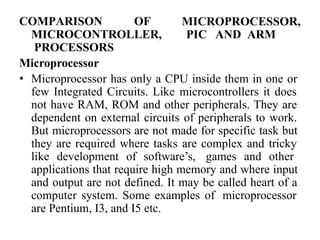
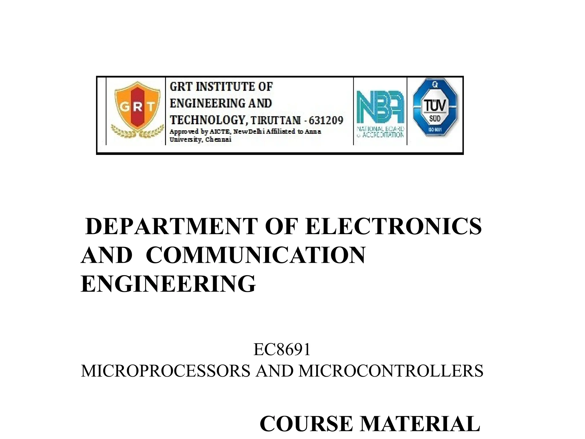
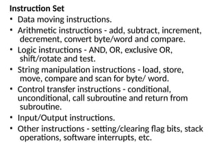
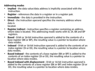
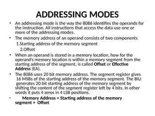
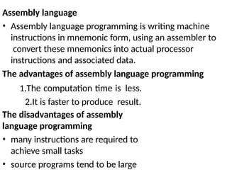
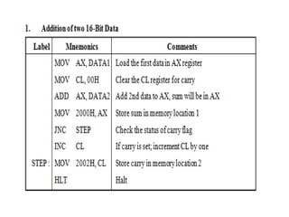
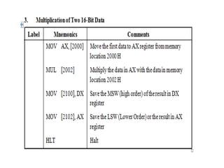
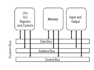
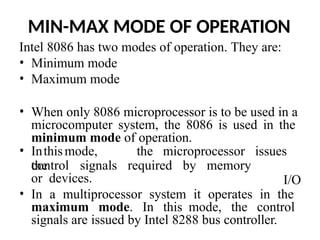
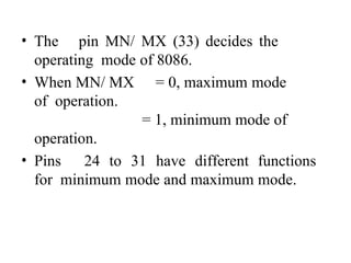
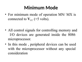
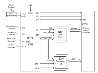
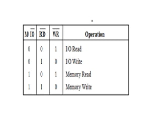
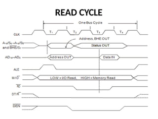
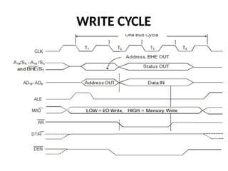
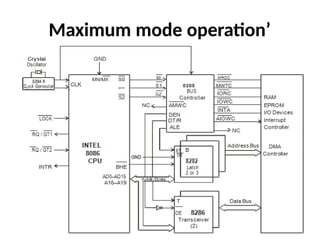
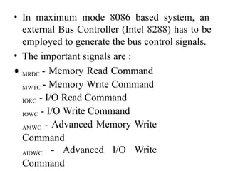
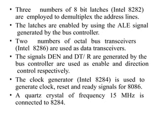
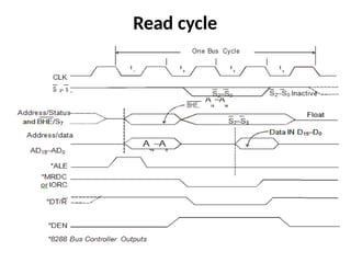
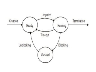
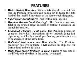
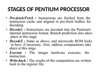
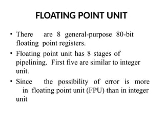
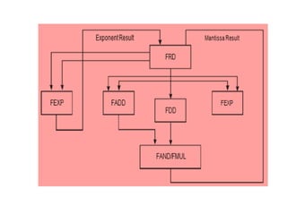
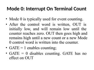
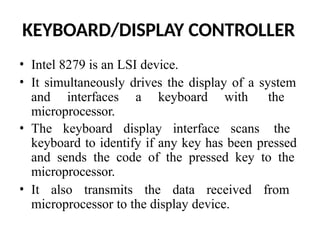
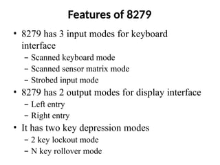
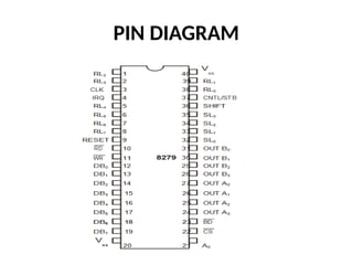
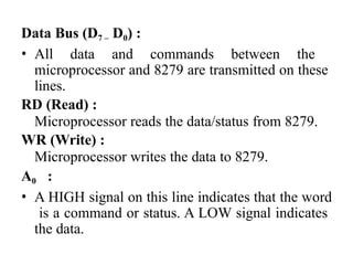
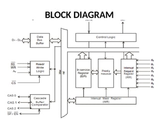
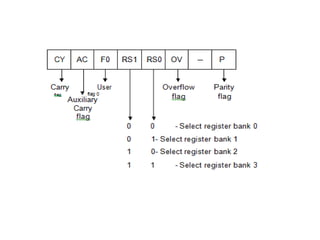
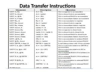
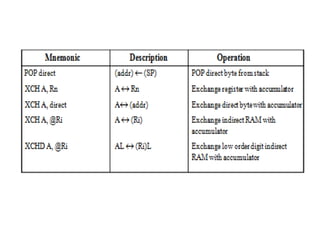
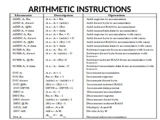
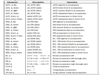
The document provides a comprehensive overview of the 8086 microprocessor, detailing its architecture, features, and operational components such as the bus interface unit and execution unit. It describes the various registers, addressing modes, and instruction sets, highlighting their functions and uses in programming. Additionally, the document explains the arithmetic, control transfer, and data manipulation instructions integral to operating the 8086 microprocessor.

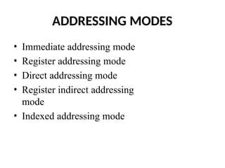
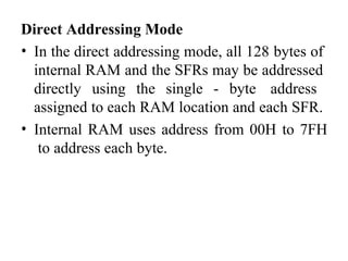
![Direct Addressing Mode
• One of the operands is a memory location, given by a
constant offset.
• In this mode the 16 bit effective address (EA) is taken
directly from the displacement field of the instruction.
• Examples:
• MOV AX,[1234 H]
• MOV DL, [3BD2 H],
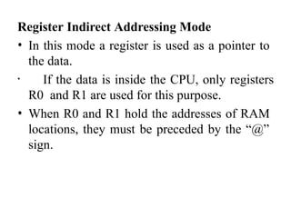
Register Indirect Addressing Mode
• One of the operands is a memory location, with the
offset given by one of the BP, BX, SI, or DI registers.
• Example:
• MOV [BX], CL
• MOV DL, [BX]](https://image.slidesharecdn.com/mpmc-ppt-240916164020-3adf143c/85/Micro-Processor-and-Micro-Controller-subject-23-320.jpg)
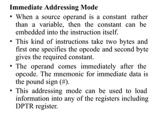
![Base Addressing Mode
• In this mode EA is obtained by adding a
displacement (signed 8 bit or unsigned 16 bit)
value to the contents of BX or BP. The segment
registers used are DS and SS.
• Example:
• MOV AX, [BP + 200]
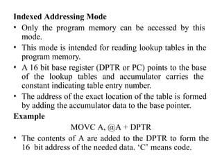
Indexed Addressing Mode
• The operand’s offset is the sum of the content of
an index register SI or DI and an 8-bit or 16-bit
displacement.
• Example:
• MOV AH, [DI]](https://image.slidesharecdn.com/mpmc-ppt-240916164020-3adf143c/85/Micro-Processor-and-Micro-Controller-subject-24-320.jpg)
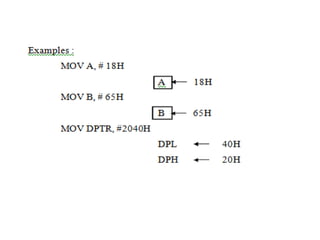
![Based Indexed Addressing Mode
• In this mode, the EA is computed by adding a base
register (BX or BP), an index register (SI or DI) and a
displacement (unsigned 16 bit or sign extended 8
bit)
• Example:
• MOV AX, [BX + SI + 1234 H]
• MOV CX, [BP][SI] + 4
String Addressing Mode
• The instruction is a string instruction, which uses
index registers implicitly to access memory.
• Example:
• MOVS B
• MOVS W](https://image.slidesharecdn.com/mpmc-ppt-240916164020-3adf143c/85/Micro-Processor-and-Micro-Controller-subject-25-320.jpg)
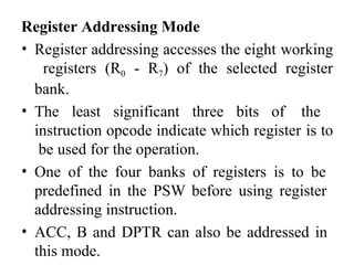
![LEA
• LEA destination, source
• This (Load Effective Address) instruction transfers the offset of the
source operand (memory) to the destination operand (16-bit
general register).
• (REG) EA
• Example :
• LEA BX, [BP] [DI]
• LEA SI, [BX + 02AF H]
LDS
• LDS destination, source
• This (Load pointer using DS) instruction transfers a 32-bit pointer
variable from the source operand (memory operand) to the
destination operand and register DS.
(EA)
(EA+2)
• (REG)
• (DS)
• Example :
• LDS SI, [6AC1H]](https://image.slidesharecdn.com/mpmc-ppt-240916164020-3adf143c/85/Micro-Processor-and-Micro-Controller-subject-35-320.jpg)
![LES
• LES destination, source
• This (Load pointer using ES) instruction transfers a 32-bit pointer variable from the
source operand (memory operand) to the destination operand and register ES.
(EA)
(EA+2)
• (REG)
• (ES)
• Example :
• LES DI, [BX]
IN
• IN accumulator, port
• This (Input) instruction transfers a byte or a word from an input port to the
accumulator (AL or AX).
• (DEST) (SRC)
• Example :
• IN AX, DX
• IN AL, 062H
OUT
• OUT port, accumulator
• This (Output) instruction transfers a byte or a word from the accumulator
(AL or AX)
to an output port.
• (DEST) (SRC)
• Example :
• OUT DX, AL
• OUT 31, AX](https://image.slidesharecdn.com/mpmc-ppt-240916164020-3adf143c/85/Micro-Processor-and-Micro-Controller-subject-36-320.jpg)
![Arithmetic Instructions
ADD
• ADD destination, source
• This (Add) instruction adds the two operands (byte or word) and stores
the result in destination operand.
• (DEST) (DEST) + (SRC)
• Example :
• ADD CX, DX
• ADD AX, 1257 H
• ADD BX, [CX]
ADC
• ADC destination, source
• This (Add with carry) instruction adds the two operands and adds one if
carry flag (CF) is set and stores the result in destination operand.
• (DEST) (DEST) + (SRC) + 1
• Example :
• ADC AX, BX
• ADC AL, 8
• ADC CX, [BX]](https://image.slidesharecdn.com/mpmc-ppt-240916164020-3adf143c/85/Micro-Processor-and-Micro-Controller-subject-37-320.jpg)
![ASSUME
• The ASSUME directive enables error-checking
for register values.
• It is used to inform the assembler the names
of the logical segments, which are to be
assigned to the different segments used in an
assembly language program
• Format:
• ASSUME segregister:name [ [, segregister:name]]...
• ASSUME dataregister:type [[, dataregister:type]]...
• ASSUME register:ERROR [[, register:ERROR]]...
• ASSUME [[register:]] NOTHING [[, register:NOTHING]]...](https://image.slidesharecdn.com/mpmc-ppt-240916164020-3adf143c/85/Micro-Processor-and-Micro-Controller-subject-67-320.jpg)
![DT (Define Ten Bytes)
• It can be used to define data like TBYTE (10 bytes).
• Format:
• Name of the Variable DT Initial values
• Example:
• AMOUNT DT 12345678123456781234
END (End of program)
• It marks the end of a program module and, optionally,
sets the program entry point to address.
• Format:
• END [ [address] ]
• Example:
• END label](https://image.slidesharecdn.com/mpmc-ppt-240916164020-3adf143c/85/Micro-Processor-and-Micro-Controller-subject-70-320.jpg)
![MACRO
• A sequence of instructions to which a name is
assigned is called a macro. The name of a macro
is used in assembly language programming.
Macros and subroutines are similar. Macros are
used for short sequences of instructions, where
as subroutines for longer ones. Macros execute
faster than subroutines. A subroutine requires
CALL and RET instructions whereas macros do
not.
• Format:
• name MACRO [ optional arguments ]
• statements ENDM](https://image.slidesharecdn.com/mpmc-ppt-240916164020-3adf143c/85/Micro-Processor-and-Micro-Controller-subject-74-320.jpg)
![OPERAND
• The operand field consists of additional information or data that the
opcode requires. In certain types of addressing modes, the operand is
used to specify
• constants or labels
• immediate data
• data contained in another accumulator or register
• an address
Examples of operands are
• JNZ STEP1
• MOV AX, 5000 H
• MOV AX, BX
• MOV AX, [3000 H]
COMMENTS
• The comment field is optional, and is used by the programmer to
explain how the coded program works. Comments are preceded by a
semi-colon. The assembler, when generating instructions from the
source file, ignores all comments.](https://image.slidesharecdn.com/mpmc-ppt-240916164020-3adf143c/85/Micro-Processor-and-Micro-Controller-subject-84-320.jpg)
![Macro definition:
name MACRO [parameters,...]
statements >
ENDM](https://image.slidesharecdn.com/mpmc-ppt-240916164020-3adf143c/85/Micro-Processor-and-Micro-Controller-subject-97-320.jpg)
![Procedure (PROC)
• This directive marks the start and end of a
procedure block called label. The statements in
the block can be called with the CALL instruction.
PROC definition:
label PROC [ [near / far] ]
<Procedure instructions>
label ENDP](https://image.slidesharecdn.com/mpmc-ppt-240916164020-3adf143c/85/Micro-Processor-and-Micro-Controller-subject-99-320.jpg)
![• Load and store strings : (LOD SB/LOD SW and STO
SB/STO SW) LOD SB: Loads a byte from a string in
memory into AL. The address in SI is used relative to
DS to determine the address of the memory location
of the string element. (AL) <= [(DS) + (SI)] (SI) <= (SI)
+ 1
• LOD SW : The word string element at the physical
address derived from DS and SI is to be loaded into
AX. SI is automatically incremented by 2. (AX) <=
[(DS) + (SI)] (SI) <= (SI) + 2
• STO SB : Stores a byte from AL into a string location
in memory. This time the contents of ES and DI are
used to form the address of the storage location in
memory [(ES) + (DI)] <= (AL) (DI) <=(DI) + 1
• STO SW : [(ES) + (DI)] <= (AX) (DI) <= (DI) + 2](https://image.slidesharecdn.com/mpmc-ppt-240916164020-3adf143c/85/Micro-Processor-and-Micro-Controller-subject-116-320.jpg)
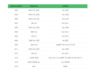
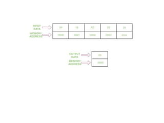
![Explanation –
• MOV SI, 500 : set the value of SI to 500
• MOV CL, [SI] : load data from offset SI to register CL
• MOV CH, 00 : set value of register CH to 00
• INC SI : increase value of SI by 1.
• MOV AL, [SI] : load value from offset SI to register AL
• DEC CL : decrease value of register CL by 1
• INC SI : increase value of SI by 1
• CMP AL, [SI] : compares value of register AL and [SI] (AL-[SI])
• JNC 413 : jump to address 413 if carry not generated
• MOV AL, [SI] : transfer data at offset SI to register AL
• INC SI : increase value of SI by 1
• LOOP 40C : decrease value of register CX by 1 and jump to address
40D if value of register CX is not zero
• MOV [600], AL : store the value of register AL to offset 600
• HLT : stop](https://image.slidesharecdn.com/mpmc-ppt-240916164020-3adf143c/85/Micro-Processor-and-Micro-Controller-subject-128-320.jpg)
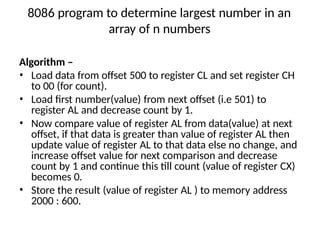
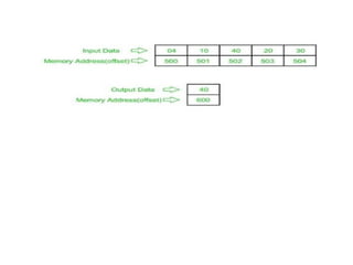
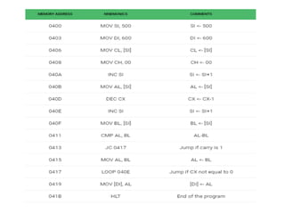
![8086 program to find the min value in
a given array
Algorithm –
• Assign value 500 in SI and 600 in DI
• Move the contents of [SI] in CL and increment SI by 1
• Assign the value 00 H to CH
• Move the content of [SI] in AL
• Decrease the value of CX by 1
• Increase the value of SI by 1
• Move the contents of [SI] in BL
• Compare the value of BL with AL
• Jump to step 11 if carry flag is set
• Move the contents of BL in AL
• Jump to step 6 until the value of CX becomes 0, and decrease CX by 1
• Move the contents of AL in [DI]
• Halt the program](https://image.slidesharecdn.com/mpmc-ppt-240916164020-3adf143c/85/Micro-Processor-and-Micro-Controller-subject-129-320.jpg)
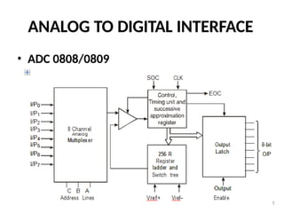
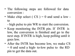
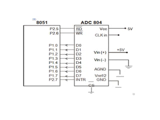
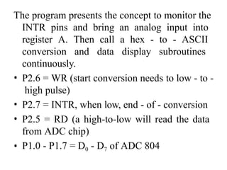
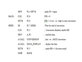
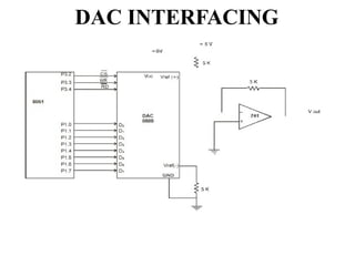
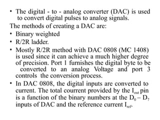
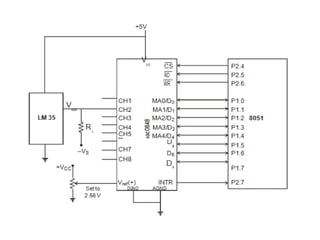
![ADC interfacing
• ADCs are used to convert the analog signals to digital
numbers so that the microcontroller can read them.
• ADC [like ADC 0804 IC] works with +5 volts and has a
resolution of 8 bits.
• Conversion time is defined as the time taken to convert the
analog input to digital (binary) number. The conversion
time varies depending upon the clock signals; it cannot be
faster than 110 μs .
• Analog input is given to the pins Vin (+) and Vin (-).
• Vin (-) is connected to ground.
• Digital output pins are D0 - D7. D7 is the MSB and D0 is the
LSB.
• There are two pins for ground, analog ground and digital
ground. Analog ground is connected to the ground of the
analog Vin and digital ground is connected to the ground of
the VCC pin.](https://image.slidesharecdn.com/mpmc-ppt-240916164020-3adf143c/85/Micro-Processor-and-Micro-Controller-subject-459-320.jpg)