November 27, 2012


Smart Materials for
Conformable Electronics
and Photonics

 Margreet de Kok
 Holst Centre
 Mikrocentrum 23 november 2012
10 november 2011
                            Presentation
                               overview
Contents


1. Holst Centre
2. Introduction OLED
3. Application of OLED
4. Lifetime of OLEDs
5. Conformable technology
6. Conclusions
© Holst Centre                                                                          4


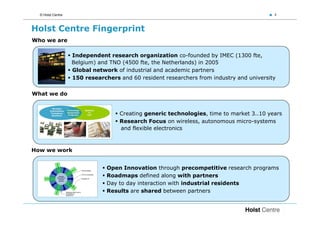
Holst Centre Fingerprint
Who we are

                   Independent research organization co-founded by IMEC (1300 fte,
                   Belgium) and TNO (4500 fte, the Netherlands) in 2005
                   Global network of industrial and academic partners
                   150 researchers and 60 resident researchers from industry and university


What we do


                                   Creating generic technologies, time to market 3..10 years
                                   Research Focus on wireless, autonomous micro-systems
                                   and flexible electronics


How we work


                               Open Innovation through precompetitive research programs
                               Roadmaps defined along with partners
                               Day to day interaction with industrial residents
                               Results are shared between partners
© Holst Centre                                                                                5


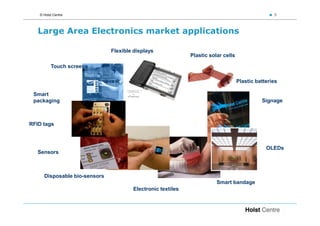
   Large Area Electronics market applications

                              Flexible displays
                                                            Plastic solar cells

         Touch screens

                                                                                  Plastic batteries

 Smart
 packaging                                                                                  Signage


RFID tags


                                                                                              OLEDs
   Sensors


     Disposable bio-sensors
                                                                       Smart bandage
                                      Electronic textiles
© Holst Centre                                                         6


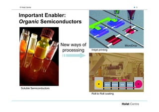
Important Enabler:
Organic Semiconductors


                          New ways of                          MicroDrop
                           processing   Inkjet printing


 Soluble Semiconductors

                                        Roll to Roll coating
© Holst Centre                                                      7


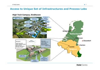
Access to Unique Set of Infrastructures and Process Labs

 High Tech Campus, Eindhoven


                                      Amsterdam

                                              Netherlands

                                                      Eindhoven
                                                                  Düsseldorf


                                                           Aachen
                                             Leuven
                                             Belgium
© Holst Centre


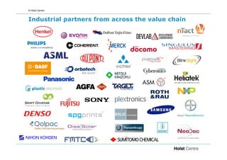
Industrial partners from across the value chain
10 november 2011


Contents
1.Holst Centre
2.Introduction OLED
3.Application of OLED
4.Lifetime of OLEDs
5.Conformable technology
6.Conclusions
© Holst Centre                                         10


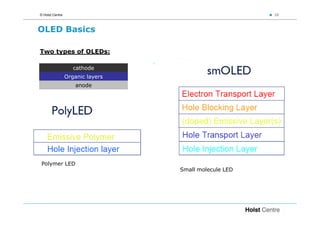
OLED Basics

Two types of OLEDs:

                    cathode
                 Organic layers
                     anode


Polymer LED
                                  Small molecule LED
© Holst Centre                                             11


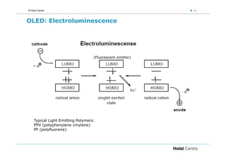
OLED: Electroluminescence


                                   (Fluorescent emitter)


    Typical Light Emitting Polymers:
    PPV (polyphenylene vinylene)
    PF (polyfluorene)
© Holst Centre                                                            12


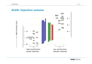
OLED: Injection scheme
                                                               SrO
                                                    BaO
                                                            Cs
                                                     LiF GdB6         2
                                                        Ba Li,K
         Work function (eV)


                                                          Ca TiN
                                                                      3
                                                               Mg
                                                          Hf
                              4         In                            4
                                             Al
                                        Ag

                              5 PEDOTNi Au
                                  ITO
                                        Pt
                                        Se TiO
                              6
                                             2


                              High workfunction   Low workfunction
                              anode materials     cathode materials
© Holst Centre                                                                                                                           13


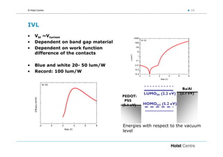
IVL
•     Vbi ~Vturnon                                                                  10000
                                                                                              BL102
•     Dependent on band gap material                                                 1000


•     Dependent on work function                                                      100

                                                                                       10
      difference of the contacts


                                                                         J (A/m )
                                                                         2
                                                                                        1

                                                                                      0.1

•     Blue and white 20- 50 lum/W                                                    0.01

                                                                                     1E-3
•     Record: 100 lum/W
                                                                                     1E-4
                                                                                         -2           0   2              4   6       8
                                                                                                              Bias (V)
                        2
                              BL102

                                                                                                                                  Ba/Al
                                                                                                LUMOPF (2.2 eV)                  (2.7 eV)
                                                                     PEDOT:
      Efficacy (lm/W)


                                                                      PSS
                        1
                                                                     (5.1 eV)                  HOMOHT (5.2 eV)


                        0
                         -2           0   2              4   6   8   Energies with respect to the vacuum
                                              Bias (V)
                                                                     level
© Holst Centre                                                      14


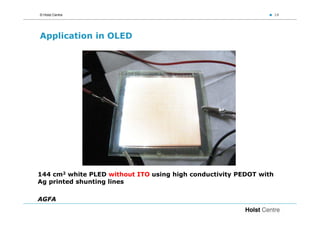
Application in OLED


144 cm2 white PLED without ITO using high conductivity PEDOT with
Ag printed shunting lines

AGFA
10 november 2011


Contents
1.Holst Centre
2.Introduction OLED
3.Application of OLED
4.Lifetime of OLEDs
5.Conformable technology
6.Conclusions
© Holst Centre                               16


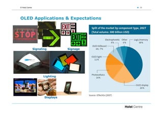
OLED Applications & Expectations


                 Signaling         Signage


                       Lighting


                        Displays
© Holst Centre                             17


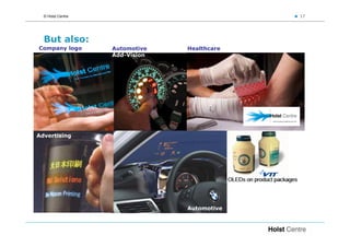
  But also:
Company logo       Automotive   Healthcare
                   Add-Vision


Advertising


                                Automotive
© Holst Centre                                  18


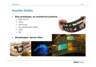
Flexible OLEDs

•     Only prototypes, no commercial products
         Add-Vision
         Sony
         Samsung
         Novaled/Assilor-Mital
         UDC
         GE

•     Showstopper: barrier films
© Holst Centre                                     19


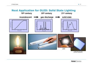
Next Application for OLED: Solid State Lighting


                                     LED

                                             (SM/P)OLED
© Holst Centre                                           20


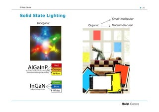
Solid State Lighting
                                       Small-molecular
                 Inorganic
                             Organic   Macromolecular


                                           OSRAM
© Holst Centre                                                                    21


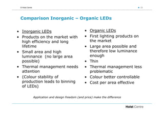
 Comparison Inorganic – Organic LEDs


• Inorganic LEDs                                      • Organic LEDs
• Products on the market with                         • First lighting products on
  high efficiency and long                              the market
  lifetime                                            • Large area possible and
• Small area and high                                   therefore low luminance
  luminance (no large area                              enough
  possible)                                           • Thin
• Thermal management needs                            • Thermal management less
  attention                                             problematic
• (Colour stability of                                • Colour better controllable
  production leads to binning                         • Cost per area effective
  of LEDs)

                  Application and design freedom (and price) make the difference
© Holst Centre                                                     22


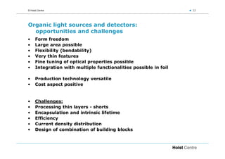
Organic light sources and detectors:
  opportunities and challenges
•     Form freedom
•     Large area possible
•     Flexibility (bendability)
•     Very thin features
•     Fine tuning of optical properties possible
•     Integration with multiple functionalities possible in foil

•     Production technology versatile
•     Cost aspect positive


•     Challenges:
•     Processing thin layers - shorts
•     Encapsulation and intrinsic lifetime
•     Efficiency
•     Current density distribution
•     Design of combination of building blocks
© Holst Centre                                                                    23


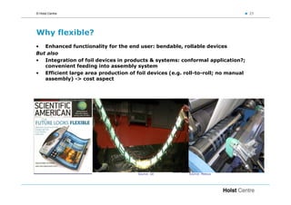
Why flexible?
• Enhanced functionality for the end user: bendable, rollable devices
But also
• Integration of foil devices in products & systems: conformal application?;
   convenient feeding into assembly system
• Efficient large area production of foil devices (e.g. roll-to-roll; no manual
   assembly) -> cost aspect


                                      Source: GE         Source: Metsuo
© Holst Centre                   24


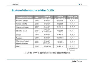
State-of-the-art in white OLED
© Holst Centre                                                                                       25


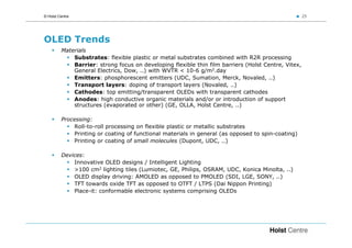
OLED Trends
         Materials
             Substrates: flexible plastic or metal substrates combined with R2R processing
             Barrier: strong focus on developing flexible thin film barriers (Holst Centre, Vitex,
             General Electrics, Dow, ..) with WVTR < 10-6 g/m2.day
             Emitters: phosphorescent emitters (UDC, Sumation, Merck, Novaled, ..)
             Transport layers: doping of transport layers (Novaled, ..)
             Cathodes: top emitting/transparent OLEDs with transparent cathodes
             Anodes: high conductive organic materials and/or or introduction of support
             structures (evaporated or other) (GE, OLLA, Holst Centre, ..)

         Processing:
             Roll-to-roll processing on flexible plastic or metallic substrates
             Printing or coating of functional materials in general (as opposed to spin-coating)
             Printing or coating of small molecules (Dupont, UDC, ..)

         Devices:
             Innovative OLED designs / Intelligent Lighting
             >100 cm2 lighting tiles (Lumiotec, GE, Philips, OSRAM, UDC, Konica Minolta, ..)
             OLED display driving: AMOLED as opposed to PMOLED (SDI, LGE, SONY, ..)
             TFT towards oxide TFT as opposed to OTFT / LTPS (Dai Nippon Printing)
             Place-it: conformable electronic systems comprising OLEDs
10 november 2011


Contents
1.Holst Centre
2.Introduction OLED
3.Application of OLED
4.Lifetime of OLEDs
5.Conformable technology
6.Conclusions
© Holst Centre     27


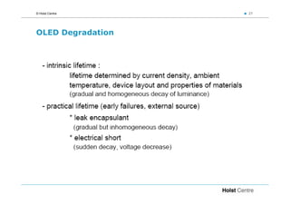
OLED Degradation
© Holst Centre     28


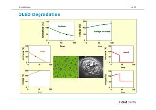
OLED Degradation
© Holst Centre                                                        29


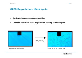
 OLED Degradation: black spots


 •     Intrinsic: homogeneous degradation

 •     Cathode oxidation: local degradation leading to black spots


                                H2O, not O2


Right after processing                        ~10h at 20 °C / 50% RH
© Holst Centre                                                          30


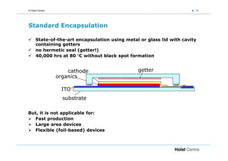
Standard Encapsulation

      State-of-the-art encapsulation using metal or glass lid with cavity
      containing getters
      no hermetic seal (getter!)
      40,000 hrs at 80 °C without black spot formation


                     cathode                    getter
                 organics

                  ITO
                   substrate

But, it is not applicable for:
  Fast production
  Large area devices
  Flexible (foil-based) devices
© Holst Centre                                 31


    Requirements for (TF) barrier/encapsulation
•     Intrinsic WVTR < 10-6 g.m-2.day-1

•     No black spots
         >5 years @ 20/50
         >504 h @ 60/90

•     Feasibility for R2R
         Barriers should be rollable over d=20cm

•     Low cost
         High deposition rates

Barrier on foil specific:
• Transparency for visible light >90%
• Uniform light output
      Extremely uniform layers over large areas
• Light outcoupling
• Abrasion resistance, UV protection, etc.
© Holst Centre                                                                                    32


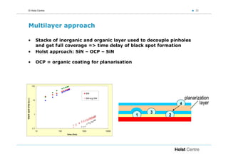
      Multilayer approach

   •                           Stacks of inorganic and organic layer used to decouple pinholes
                               and get full coverage => time delay of black spot formation
   •                           Holst approach: SiN – OCP – SiN

   •                           OCP = organic coating for planarisation


                         100


                                                              SiN

                                                              SiN-org-SiN                         planarization
black spot area (a.u.)


                         10

                                                                                                4         layer
                                                                                        3
                           1
                                                                                    1       2

                         0.1
                               10       100                1000             10000
                                              time (hrs)
© Holst Centre                                                       33


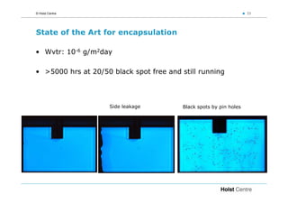
State of the Art for encapsulation

• Wvtr: 10-6 g/m2day

• >5000 hrs at 20/50 black spot free and still running


                     Side leakage         Black spots by pin holes
© Holst Centre                                         34


Advanced systems by combined functionalities in Foil

•     Organic LEDs
•     Organic Photodetectors
•     Organic Photovoltaics
•     Embedded circuitry
•     Embedded chips
•     RFID
•     Memories

•     Sensors
         Electrochemical
         Optochemical
         Optical
© Holst Centre                                                                                                                       35         35


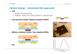
Device Design - laminated foil approach
•     Foil
          Double side processing
          Modular: diodes and LEDs printed on separate foils

•     Top emissive PLEDs, Bottom receptive OPDs:

                                                                                                                    Photodiode
                                   skin
                                                                                     LED


•     Bottom emissive PLEDs, Top receptive OPDs:

                                   skin


                                                                                                   30


                                                                Spectral Radiance (10 W/sr m nm)
                                                               2
                                                                                                   25

                                                                                                   20


                                                               -3
•     Etc.                                                                                         15

                                                                                                   10

                                                                                                   5

                                                                                                   0
                                                                                                        500   550    600    650    700    750
                                                                                                                     wavelength (nm)
© Holst Centre                                           36   36


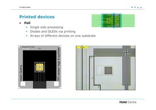
Printed devices
•     Foil
          Single side processing
          Diodes and OLEDs via printing
          Arrays of different devices on one substrate
© Holst Centre                    37   37


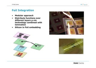
Foil Integration
•     Modular approach
•     Distribute functions over
      different layers µ-via
      technology combined with
      lamination
•     Silicon in Foil embedding
© Holst Centre                                                                               38      38


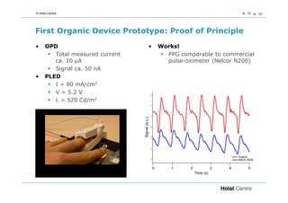
First Organic Device Prototype: Proof of Principle
•     OPD                                     •       Works!
         Total measured current                         PPG comparable to commercial
         ca. 10 µA                                      pulse-oximeter (Nelcor N200)
         Signal ca. 50 nA
•     PLED
         I = 80 mA/cm2
         V = 5.2 V
         L = 520 Cd/m2


                                  Signal (a.u.)

                                                                                       Organic
                                                                                       Nelcor N200


                                                  0       1     2              3   4          5
                                                                    Time (s)
10 november 2011


Contents
1.Holst Centre
2.Introduction OLED
3.Application of OLED
4.Lifetime of OLEDs
5.Conformable technology
6.Conclusions
© Holst Centre                     40


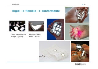
 Rigid –> flexible -> conformable


Glass based OLED   Flexible OLED
Philips Lighting   Holst Centre
© Holst Centre


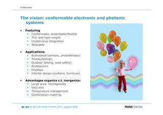
The vision: conformable electronic and photonic
  systems
•     Featuring
          Conformable, stretchable/flexible
          Thin and light weight
          Unobtrusive integration
          Wearable

•     Applications:
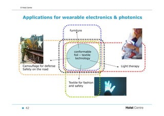
         Biomedical (sensors, phototherapy)
         Textile/fashion,
         Outdoor (biking, road safety)
         Architecture
         Displays
         Interior design (curtains, furniture)

•     Advantages organics c.t. inorganics:
         Large area: homogeneity
         Very thin
         Temperature management
         Combination inspiring


 Margreet de Kok Holst Centre 2011 august SPIE
    41
© Holst Centre


  Applications for wearable electronics & photonics

                           furniture


                               conformable
                               foil – textile
                                technology

  Camouflage for defense                         Light therapy
  Safety on the road


                           Textile for fashion
                           and safety


      42
© Holst Centre                                   43


Healing power of sunlight: wearable phototherapy


   TBC treatment by sun therapy
© Holst Centre                                                                 44


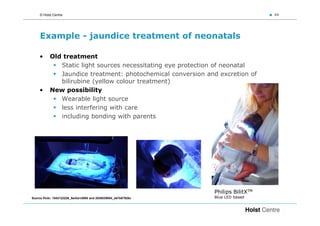
     Example - jaundice treatment of neonatals

    •      Old treatment
              Static light sources necessitating eye protection of neonatal
              Jaundice treatment: photochemical conversion and excretion of
              bilirubine (yellow colour treatment)
    •      New possibility
              Wearable light source
              less interfering with care
              including bonding with parents


                                                                 Philips BilitXTM
Source flickr: 1542122226_5e43a1d008 and 2538039854_e67b67926c   Blue LED based
© Holst Centre                                             45


Other options for applications

•     Light in safety (traffic, working conditions)
•     Light harvesting (tents, outdoor sports, clothing)
•     Phototherapy:
         psoriasis,
         eczema,
         jaundice,
         wound healing,
         prevention decubitus,
         pain relief,
         skin rejuvenation
•     Camouflage
•     Textile design – fashion!

•     Bring light where no light was before
© Holst Centre


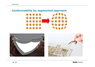
Conformability by segmented approach


      46
© Holst Centre                                                      47


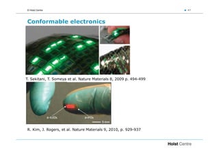
Conformable electronics


T. Sekitani, T. Someya et al. Nature Materials 8, 2009 p. 494-499


R. Kim, J. Rogers, et al. Nature Materials 9, 2010, p. 929-937
© Holst Centre                                                      48


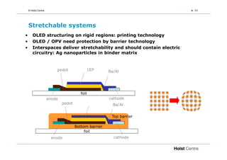
    Stretchable systems
•      OLED structuring on rigid regions: printing technology
•      OLED / OPV need protection by barrier technology
•      Interspaces deliver stretchability and should contain electric
       circuitry: Ag nanoparticles in binder matrix


                         pedot                 LEP    Ba/Al


                                        foil
                     anode                            cathode
                             pedot                      Ba/Al


                                                       Top barrier

                                     Bottom barrier
                                          foil
                      anode                             cathode
© Holst Centre                                                                  49


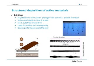
Structured deposition of active materials
•    Printing:
         Inkjetable ink formulation (halogen-free solvent): droplet formation
         Jetting and stable in time & speed
         Ink & substrate interaction
         Layer formation and homogeneity
         Device performance and efficiency
© Holst Centre                                  50


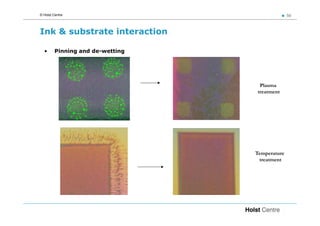
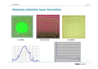
Ink & substrate interaction

  •      Pinning and de-wetting


                                   Plasma
                                  treatment


                                  Temperature
                                   treatment
© Holst Centre                                51


Solvents selective layer formation


          A 100%   A:B=50:50         B 100%
© Holst Centre                                        52


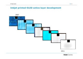
Inkjet printed OLED active layer development


            2007


                                               2011
© Holst Centre     53


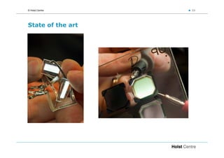
State of the art
© Holst Centre


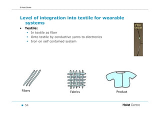
Level of integration into textile for wearable
  systems
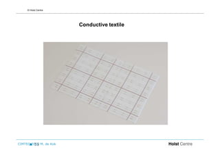
•     Textile:
         In textile as fiber
         Onto textile by conductive yarns to electronics
         Iron on self contained system


    Fibers                         Fabrics                 Product


      54
© Holst Centre


CIMTEC 2012 M. de Kok
         55
© Holst Centre                             56


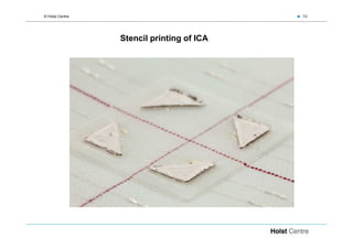
                 Stencil printing of ICA
© Holst Centre                              57


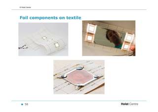
                 Bonded OLED onto textile
© Holst Centre


Foil components on textile


      58
© Holst Centre


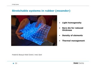
Stretchable systems in rubber (meander)


                                             •   Light homogeneity

                                             •   Bare die for reduced
                                                 thickness

                                             •   Density of elements

                                             •   Thermal management


Frederick Bossuyt Holst Centre / imec Gent


      59
© Holst Centre                    60


        Platform for Large Area
        Conformable Electronics
        by InTegration
        FP7 Place-it


                                  60
10 november 2011


Contents
1.Holst Centre
2.Introduction OLED
3.Application of OLED
4.Lifetime of OLEDs
5.Conformable technology
6.Conclusions
© Holst Centre                                              62


Conclusions

•     Organic electronics on textile have a bright future
•     Technology development indispensable
•     Collaboration between disciplines necessary

•     Conformable electronics will change the world


•     Margreet.dekok@tno.nl
•     www.holstcentre.com

•     Thank you for your attention
Visit us at
www.holstcentre.com