Evolution of Computer
architecture
2
CPU Architecture
• There are four factors influencing CPU
evolution:
– Technology (constraint or opportunity)
– Theory and design inginuity
– User demand
– Economics & commercial pressure
3
Technology
Relays, Thermionic valve, Diodes and Bipolar
Transistors, RTL then TTL integrated circuits,
MOS integrated circuits, LSI and VLSI
4
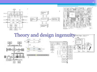
Theory and design ingenuity
5
User Demand
6
Economics & Commercial Pressure
7
CPU Architecture
• In the decade 1943 (ENIAC) to 1953 (IBM 701)
theory, engineering design, technological
inginuity flourished.
• The 2nd World War brought together key actors
and lent an urgency to their work, this was
followed by a commercial race to bring the new
developments to the market
• The decade ends just as the first Si transistor
designs and magnetic core memory were
introduced.
• Here are some key developments:
8
CPU Architecture
Eckert & Mauchley ENIAC:
Begun 1943 finished 1946
5000 operations a second
Programmed by
plugboard & switches
I/O: card, lights, plugs, switches
Size: floor area 100 sq metres
9
CPU Architecture
Colossus 1. 1944
Used for code breaking by
the British
Programmed by
Patch cord and switches
I/O: paper tape, teleprinter
1500 thermionic valves
5000 operations a second
Reliability?: Never switched
off unless malfunctioned.
Followed by Colossus Mk2,
2400 valves, 25000
operations a second
10
CPU Architecture
Harvard Mark 1 1944: Electromechanical, programmable (really an
automatic calculator),16m long, 2m high, more reliable than contempary valve
machines
11
CPU Architecture
EDSAC. 1949
First practical programmable
stored program computer
1k words of memory
17 bit word
Mercury delay line memory
700 operations a second
I/O: punched tape, teleprinter
Programmed by a primitive assembler
set-up by hand on uniselectors and
transferred into memory.
Wilkes: Cambridge University Mathematics Lab
12
CPU Architecture
• "Computers in the future may weigh no more
than 1.5 tons."
-Popular Mechanics, 1949
b
13
CPU Architecture
“From then on, when
anything went wrong
with a computer, we said
it had bugs in it (an
error in the 1940s
Harvard mark 11
computer was traced
to a moth trapped inside).”
- Rear Admiral Grace
Murray Hopper, US Navy
14
CPU Architecture
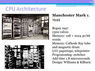
Manchester Mark 1.
1949
Begun 1947
1300 valves
Memory: 128 + 1024 40 bit
words
Memory: Cathode Ray tube
and magnetic drum
I/O: papertape, teleprinter
Programming: switches
Add time 1.8 microseconds
Design: Williams & Kilburn
15
CPU Architecture
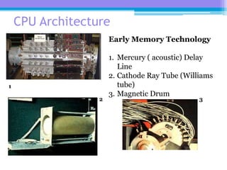
Early Memory Technology
1. Mercury ( acoustic) Delay
Line
2. Cathode Ray Tube (Williams
tube)
3. Magnetic Drum
1
2 3
16
CPU Architecture
• All these memory devices operate as a long shift
register. No random access.
Data enters, takes some time to travel to the output and is recirculated.
Data can only be read as it reaches the output – there is a waiting time,
latency, for it to appear. Storage is achieved by this I/O delay and
recirculation.
Mercury delay line – acoustic delay. Williams tube – phosphor persistence.
Magnetic drum – diameter and speed.
Data in mercury delay line and cathode ray tube is volatile, if not recirculated
it is lost. Magnetic drum is non-volatile.
17
CPU Architecture
SEAC 1950
Diode logic
10500 diodes and 1500 valves
Mercury delayline memory
512 words 45 bits
Clock 1MHz
Add 864 microseconds
Magnetic Tape external storage
I/O: teleprinter or mag tape
& remote teleprinter
Used for scientific calculation:
Meteorology, navigation etc..
18
CPU Architecture
ACE 1950
Start of project:1948
Completed:1950
Add time:1.8 microseconds
Input/output:cards
Memory size:352 32-digit words
Memory type:delay lines
Technology:800 valves
Floor space:1.5 sq metres
Project leader:J. H. Wilkinson
19
CPU Architecture
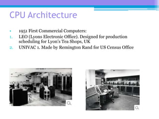
• 1951 First Commercial Computers:
1. LEO (Lyons Electronic Office). Designed for production
scheduling for Lyon’s Tea Shops, UK
2. UNIVAC 1. Made by Remington Rand for US Census Office
20
CPU Architecture
• Speed:1,905 operations
per second
• Input/output:magnetic
tape, unityper, printer
• Memory size:1,000 12-
digit words
• Memory type:delay lines,
magnetic tape
• Technology:valves
• Floor space:11 sq metres
• Cost: approx $1million
• Project leaders:Eckert
and Mauchley
UNIVAC 1. 1951
21
CPU Architecture
Clock 500kHz Instruction time 1.5 ms
Multiple I/O streams
I/O: paper tape & punch,
card reader & punch, mag tape
Memory: mercury delay line
2048 35 bit words
Initially used for production planning,
later for inventory and payroll –
1st MIS
LEO 1951
22
CPU Architecture
IBM 701. 1953
IBM’s first commercial scientific computer. 19 were sold.
KOMPILER compiler and run-time environment, later FORTRAN
Memory 2048 36 bit words (expandable to 4096)
Multiply/divide 456 microseconds
23
CPU Architecture
Magnetic Core Memory.
First used in Whilrwind computer 1953
First Random Access memory. Non-volatile.
Faster and more reliable than earlier memory technology
24
CPU Architecture
Memory access is as a read/write cycle
Required address is decoded as X & Y coordinates and a current pulse applied
If the core where X & Y are coincident is a 0 no signal on the sense line, if a 1 the
magnetic state of the core is flipped and there is a sense pulse
This read is destructive so the data has to be written back
Magnetic core memory is non-volatile
Magnetic Core Memory
25
CPU Architecture
1954. Silicon Transistor
Texas Instruments
1955. TRADIC Bell Labs
First transistorized computer
800 transistors 10000 diodes
Power less than 100 Watts
(a twelfth power required by valves)
In the photo a program is being
Loaded via a plugboard
26
CPU Architecture
• These machines, though of varying architecture
and capability, have features that have been
absorbed and re-used in the computers that
followed. There are very few ideas or features
that have been introduced since that are not
echoes of what went before.
27
CPU Architecture
• The next era is that of the Mainframe.
• Bigger, more powerful, and expensive.
• Two main applications: business
• applications, accounting, MIS…..
• and scientific applications requiring vast
• numbers of simple calculations…..
• And later the Minicomputer was developed
28
CPU Architecture
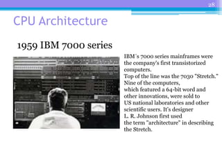
IBM´s 7000 series mainframes were
the company's first transistorized
computers.
Top of the line was the 7030 "Stretch."
Nine of the computers,
which featured a 64-bit word and
other innovations, were sold to
US national laboratories and other
scientific users. It’s designer
L. R. Johnson first used
the term "architecture" in describing
the Stretch.
1959 IBM 7000 series
29
CPU Architecture
1960 DEC PDP1
50 were build, cost $120,000.
It had a cathode ray tube graphic display,
needed no air conditioning and required
only one operator.
The display intrigued early hackers at MIT,
who wrote the first computerized video game,
SpaceWar!, for it. SpaceWar became
The standard demonstration on all 50.
30
CPU Architecture
Fairchild invented the resistor-transistor
logic (RTL).
The first product a set/reset flip-flop
and the first integrated circuit available
as a monolithic chip.
1961 RTL ICs
31
"But what...is it good for?"
-Engineer at the Advanced Computing
Systems Division of IBM, 1968,
commenting on the microchip
32
CPU Architecture
• 1963 to 1966 TTL
• Transistor Transistor
Logic.
• First introduced by
Sylvania for US military
• Commercial devices by
Texas Instruments 7400
family.
33
CPU Architecture
1964 IBM System/360
IBM System/360:
a family of six mutually compatible computers
and 40 peripherals that could work together.
The initial investment of $5 billion was
quickly returned as orders for the system
climbed to 1,000 per month within two years.
At the time IBM released the System/360,
the company was making a transition from
discrete transistors to integrated circuits,
and its major source of revenue moved
from punched-card equipment to electronic
computer systems.
34
CPU Architecture
Digital Equipment Corp. introduced the PDP-8,
the first commercially successful minicomputer.
The PDP-8 sold for $18,000, one-fifth the price
of a small IBM 360 mainframe. The speed,
small size, and reasonable cost enabled the
PDP-8 to go into thousands of manufacturing
plants, small businesses, and scientific
laboratories.
1965 DEC PDP8
35
CPU Architecture
• Virtually all these machines have recognizable
architecture based Turing Machine and von
Neumann architecture.
• Here’s an examples that differ and points to
modern Supercomputers.
36
CPU Architecture
CDC´s 6600 supercomputer, designed by
Seymour Cray, performed up to 3 million
instructions per second.
The 6600 retained the distinction of being
the fastest computer in the world until surpassed
by its successor, the CDC 7600, in 1968.
Part of the speed came from the computer's
design, which had 10 small computers, known
as peripheral processors, funneling data to a
large central processing unit.
1964 CDC 6600
37
CPU Architecture
Hewlett-Packard entered the general purpose
computer business with its HP-2115, offering
a computational power formerly found only
in much larger computers.
It supported a wide variety of languages,
among them BASIC, ALGOL, and FORTRAN.
The photo shows the familiar teleprinter for
papertape I/O and printer for output.
The CPU with binary display and switches.
Thes second box is core memory
1966 HP-2115
38
CPU Architecture
Fairchild produced the first standard
metal oxide semiconductor MOS product
for data processing applications, an
eight-bit arithmetic unit and accumulator.
1967 1st data processing MOS ic
39
CPU Architecture
Data General Corp., started by a group of
engineers that had left DEC., introduced
the Nova, with 32 kilobytes of memory,
for $8,000.
In the photograph, Ed deCastro,
president and founder of Data General,
sits with a Nova minicomputer.
The simple architecture of the Nova
instruction set inspired Steve Wozniak´s
Apple I board eight years later.
1968 DG Nova
40
CPU Architecture
• This brings us to the dawn of the Microprocessor
era – a convenient point to discuss the
underlying theory:
• Binary data
• Turing Machine
• Von Neumann architecture
• Basic CPU architecture
41
CPU Architecture
• Binary Data
• Data and other information is stored and
processed by electronic circuits that have only
two states (0/1:Lo/Hi:OFF/ON). Bits.
• Several bits together represent the data
according to standard coding systems. Words.
• 01100001=a in ASCII
42
CPU Architecture
A thought experiment by the English Mathemetician Alan Turing in 1936.
Decisions are based on the current state (the result of what happened before)
and the data being read, the “head” moves back and forth based on this decision.
This encapsulates the action of a digital computer’s CPU, the current state and
new data are manipulated according to an instruction and what happens next is
determined.
43
CPU Architecture
Von Neumann architecture.
Data and instructions are stored
in memory, the Control Unit
takes instructions and controls
data manipulation in the
Arithmetic Logic Unit.
Input/Output is needed to make
the machine a practicality
Memory
Control ALU
I/O
44
CPU Architecture
CPU Architecture
The ALU manipulates
two binary words according
to the instruction decoded
in the Control unit. The
result is in the Accumulator
and may be moved into
Memory.
45
CPU Architecture
• von Neumann architecture introduces a problem, which
is not solved until much later.
• The CPU work on only one instruction at a time, each
must be fetched from memory then executed. During
fetch the CPU is idle, this is a waste of time. Made worse
by slow memory technology compared with CPU.
• Time is also lost in the CPU during instruction decode.
F E F E --------- D E
46
CPU Architecture
• Take a closer look at the action part of the CPU,
the ALU, and how data circulates around it.
• An ALU is combinational logic only, no data is
stored, i.e. no registers. This is the original
reason for having CPU registers.
• By convention the output of a CPU is stored in
the Accumulator¹, but what about the inputs?
• ¹Accumulator because original ALUs worked one bit at a time and
“accumulated” the answer
47
CPU Architecture
CPU Architecture
ALU
A
X Y
In the simplest, minimum
hardware, solution one of them,
say X, is the accumulator A, the
other, Y, is straight off the memory
bus (this requires a temporary
register not visible to the
programmer).
The instruction may be ADDA,
which means: add to the contents
of A the number (Y) and put the
answer in A.
data bus
48
CPU Architecture
• It’s a simple step to add more CPU data registers
and extend the instructions to include B, C,….. as
well as A.
• An internal CPU bus structure then becomes a
necessity, but how many busses? Designs exist
with 1,2, or 3.
(Look up the details if you’re interested.)
49
CPU Architecture
50
CPU Architecture
• Bus A delivers data to
• one input of the ALU
• bus B the other, the
• convention of the ALU
• output going to A
• usually holds.
• Connections to the data
bus
• not shown. You can work
• out how a 1 or 3 bus
system
• would work.
A
B
N
ALU
bus A bus B
51
CPU Architecture
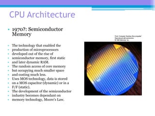
• 1970?: Semiconductor
Memory
• The technology that enabled the
• production of microprocessors
• developed out of the rise of
• semiconductor memory, first static
• and later dynamic RAM.
• The random access of core memory
• but occupying much smaller space
• and costing much less.
• Uses MOS technology, data is stored
• on a MOS capacitor (dynamic) or in a
• F/F (static).
• The development of the semiconductor
• industry becomes dependant on
• memory technology, Moore’s Law.
52
CPU Architecture
• We’ve reached the point at which the first
microprocessors appear: 1971 INTEL 4004
The first advertisement for a
microprocessor, the Intel 4004, appeared
in Electronic News. Developed for Busicom,
a Japanese calculator maker, the 4004 had
2250 transistors and could perform up to
90,000 operations per second in four-bit
chunks. Federico Faggin led the design and
Ted Hoff led the architecture.
INTEL realized they had a good idea and
extended it to a general purpose device…..
53
CPU Architecture
1972: INTEL 8008
A vast improvement over the
4004, its eight-bit word afforded
256 unique arrangements of ones
and zeros. For the first time, a
microprocessor could handle
both uppercase and lowercase
letters, all 10 numerals,
punctuation marks, and a host of
other symbols, as in ASCII.
And led to the early microcomputers….
54
CPU Architecture
1973: Micral
The Micral was the earliest commercial, non-
kit personal computer based on a micro-
processor, the Intel 8008. Thi Truong
developed the computer and Philippe Kahn
the software. Truong, founder and president
of the French company R2E, created the
Micral as a replacement for minicomputers in
situations that didn´t require high
performance. Selling for $1,750, the Micral
never penetrated the U.S. market. In 1979,
Truong sold Micral to Bull.
There are other very early microcomputers, see:
www.digibarn.com/stories/bill-pentz-story/index.html
The 8008 was quickly followed by the more
functional 8080….
55
CPU Architecture
1975: Altair 8800
The January edition of Popular Electronics
featured the Altair 8800 computer kit,
based on Intel 8080 microprocessor, on its
cover. Within weeks of the computer's
debut, customers inundated the
manufacturing company, MITS, with
orders. Bill Gates and Paul Allen licensed
BASIC as the software language for the
Altair. Ed Roberts invented the 8800 —
which sold for $297, or $395 with a case —
and coined the term "personal computer."
The machine came with 256 bytes of
memory (expandable to 64K) and an open
100-line bus structure that evolved into the
S-100 standard.
56
CPU Architecture
1976: Apple 1
Steve Wozniak designed the Apple I,
a single-board computer. With an
order for 100 machines at $500 each
from the Byte Shop, he and Steve
Jobs got their start in business. In
this photograph of the Apple I board,
the upper two rows are a video
terminal and the lower two rows are
the computer. The 6502
microprocessor in the white package
sits on the lower left. About 200 of
the machines sold before the Apple 2
was introduced.
57
CPU Architecture
1976 also saw the introduction a famous
supercomputer the Cray 1.
It made its name as the first
commercially successful vector
processor. The fastest machine of its
day, its speed came partly from its
shape, a C, which reduced the length of
wires and thus the time signals needed
to travel across them. The electronics
generated a lot of heat needing liquid
cooling the mechanism for forms the
seating around the base.
Project started:1972 completed:1976
Speed:166 million floating-point
operations per second
Size:58 cubic feet Weight:5,300 lbs.
Technology: Integrated circuit ECL
Clock rate:83 MHz Word length:64-bits
Instruction set:128 instructions
1976 Cray 1
58
CPU Architecture
more info: http://www.z80.info/zip/z80pps.zip
The Zilog Z-80 could run any
program written for the 8080.
It had many features that made
it useful in microcomputers to
run HLLs, many extra
instructions and two sets of
CPU registers.
1976 Zilog Z80
59
CPU Architecture
The Commodore PET (Personal Electronic
Transactor) — the first of several personal computers
released in 1977 — came fully assembled and was
straightforward to operate, with either 4 or 8
kilobytes of memory, two built-in cassette drives, and
a membrane "chiclet" keyboard.
The Apple II became an instant success when
released in 1977 with its printed circuit motherboard,
switching power supply, keyboard, case assembly,
manual, game paddles, A/C powercord, and cassette
tape with the computer game "Breakout." When
hooked up to a color television set, the Apple II
produced brilliant color graphics.
1977 Commodore PET, APPLE II
60
CPU Architecture
1978: DEC VAX 11/780
The VAX 11/780 from DEC featured the
ability to address up to 4.3 gigabytes of
virtual memory, providing hundreds of
times the capacity of most
minicomputers,
But essentially marks the end of the
Minicomputer era.
61
CPU Architecture
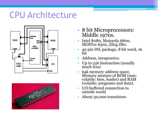
• 8 bit Microprocessors:
Middle 1970s.
• Intel 8080, Motorola 6800,
MOSTec 6502, Zilog Z80.
• 40 pin DIL package, 8 bit word, 16
bit
• Address, inexpensive.
• Up to 256 Instruction (usually
much less)
• 64k memory address space.
Memory mixture of ROM (non-
volatile: bios, loader) and RAM
(volatile: programs and data).
• I/O buffered connection to
outside world
• About 30,000 transistors
62
CPU Architecture
Address Bus 16 bits
Data Bus 8 bits
Control signals
System Architecture
8bit Micro
63
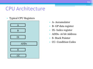
CPU Architecture
• Typical CPU Registers
• A- Accumulator
• B- GP data register
• IX- Index register
• ADDs- 16 bit Address
• S- Stack Pointer
• CC- Condition Codes
A
B
IX
ADDs
S
CC
64
CPU Architecture
• Typical Instruction Set
• Data: arithmetic and logical manipulation of data.
Result into A or sets CCs
• Load/Store: Move data/addresses in and out of
registers
• Program: branch, jump, push, pull, interrupt, return,
NOOP
65
CPU Architecture
• Typical Addressing Modes: Where is the data?
• Direct: in register
• Immediate: in the program
• Implied: the instruction tells e.g DECA
• Absolute/Zero page: at the address (16 or 8 bit)
• Relative: offset from where you are now
• Indexed: at address incremented content of index reg
• and often combinations of the above
66
CPU Architecture
• Though these 8 bit micros led to the
development of the general purpose personal
computer the limited number of CPU registers,
limited address space and simple addressing
modes led to problems.
• How do you enable users to program in an HLL
when you need an operating system and maybe a
BIOS underneath without constantly swapping
register content in and out of memory?
• (The Z80 partially solved this by having two sets of CPU
registers, other solutions relied on compiling HLL into
machine code as early mainframes had done.)
67
CPU Architecture
The Motorola 68000 microprocessor
exhibited a processing speed far greater
than its contemporaries. This high
performance processor found its place in
powerful work stations intended for
graphics-intensive programs common in
engineering.
1979: 16 bit Microprocessors
16 bit micros were designed for use in
microcomputer. More general purpose
registers, bigger address space, more
possible levels of indirection in addressing
to allow virtual addresses. About 200,000
transistors
68
CPU Architecture
Another requirement of HLLs was the ability to carry out floating point maths,
programming the algorithms was tedious and execution slow – hence the idea of a
co-processor with hardware for FP maths. This is the INTEL 8087 introduced in
1980 Maths co-processor for the 8088. The maths processor eventually become
part of the CPU.
69
CPU Architecture
1981: The IBM PC
IBM introduced its PC, igniting a fast growth of the personal computer
market. The first PC ran on a 4.77 MHz Intel 8088 microprocessor and used
Microsoft´s MS-DOS operating system.
Evolution of Processors
71
Intel vs AMD
72
Part 1: Comparative History
• Generally Intel has been the dominant
producer
of microprocessor chips
• AMD has proven to be a fierce competitor
• Competition stimulated the industry by
producing new and innovative
microprocessors
• In the mid nineties Intel begins to face true
competition
73
Comparative History
– 80286 chip
• 1980’s-Intel was the only true producer of
marketable computer chips
• 1982-introduce 80286
• 286 was able to run software of its prior
microprocessor
74
Comparative History
– 80286 chip
• Within 6 years, 15 million 286’s are installed
around the world
• Intel contracts third party companies to produce
286’s and variants
• AMD was one of these third party companies
• AMD became very efficient and capable of being
its own producer of microprocessors
75
Comparative History
– 386 chip
• 1985, Intel releases its 32-bit 386 microprocessor.
• Faster and capable of multitasking
• AMD, under licensed production, produces 386 chips
allowing Intel to meet market demands
76
Comparative History
– 386 chip
• During the reign of the 386, AMD decides to
produce
its own CPU.
• 1987-AMD began legal arbitration over rights to
produce their own chips.
• After 5 years of battle, the courts sided with
AMD.
77
Comparative History
-486 chip
• 1989-Intel releases its 486DX.
• Allowed point and clicking
• Initially twice as fast as its predecessor.
• Intel continued to upgrade to speeds reaching
66MHz.
78
Comparative History
-Am386 chip
• 1991-AMD released Am386
• Intel’s 486 released two years prior
• AMD believed there still existed a market
• By October, AMD sold one million units
79
Comparative History
-Am486 chip
• 1993-AMD releases first competing chip: Am486
• 1994-AMD improves chip with Am486DX
• Am486DX processes up to 100MHz
Comparative History
-Pentium
• 1993, Intel realizes it cannot trademark numbers
“x86.”
• This allows AMD the ability to essentially clone
Intel’s chips
• Intel’s solution: dubs its new chip the Pentium
instead of releasing it as the “586”
Comparative History
-Pentium
• Handles and processes more media types such
as speech, sound , and photographic images.
• It Offered multiple processing speeds up
to 200MHz.
• It became well entrenched in the market
• During this time, Intel truly dominated
Comparative History
-Am5x86
• 1995- AMD’s first attempt to compete with the
Pentium by introducing Am5x86
• It was really for those who wanted to upgrade
their 486 motherboards without making a jump
to the Pentium motherboard
• AMD did not fare well with this chip
Comparative History
-AMD K5
• 1996-K5 introduced
• First chip comparable to the Pentium
• Could be placed in the same motherboard as
the Pentium, making it compatible
• Because it was released 3 years after the
Pentium, it was met with cool reception
Comparative History
-Pentium Pro
• In the previous year, Intel released the Pentium
Pro
• Able to handle more instructions per clock cycle
• Intel’s ability to get a new chip on the market
before AMD has had the effect of overshadowing
any of AMD’s microprocessors
Comparative History
-AMD K6
• 1996-AMD purchases the company NexGen who
were making a microprocessor of their own
• AMD uses their core 686 processor to develop
the AMD K6
• Additionally, they slap on Intel’s MMX code
making it compatible with Pentiums.
Comparative History
-AMD K6
• K6 was released in 1997 and reached speeds of
166Mhz to 200Mhz
• K6 was significantly cheaper than the Pentium
• K6 was able to move up to speeds as high as
300MHz, out performing the Pentiums
• Intel was ready for the challenge
Comparative History
-Pentium II
• Later than year, Intel unveils the Pentium II
• It was equipped with MMX instructions, ready
to handle video, audio, and graphics data
• Better capable of handling video editing, sending
media via the Internet, and reprocessing music
• By 1998, the Pentium began to climb in
processing speeds up to 450 MHz.
Comparative History
-The Celeron
• K6 was doing well as a cost effective alternative to
the Pentium II, although it was an inferior chip
• In response, in 1998, Intel introduced its own
cheaper and inferiror microprocessor: the Celeron
• It was a stripped down version of the Pentium II
Comparative History
-AMD’s K6-2
• AMD fights back with an enhanced K6 to take on the
Pentium II: the K6-2
• Their K6 chip included what they called “3DNow”
technology
• 3DNow is an additional twenty-two instructions to
better handle audio, video, and graphic intensive
programs
• AMD then releases K6-3 and proves to be a threat to
Intel
Comparative History
-Pentium III
• 1999-Intel responds by coming out with the
Pentium III
• It had an additional 70 instructions, improving its
ability to process advanced imaging, streaming
audio, video, & speech recognition programs
• One goal of the Pentium III was to enhance the
Internet experience
Comparative History
-the Athlon
• The Athlon was a new chip from the ground up
• It was capable of doing everything the Pentium III
could do, but was much cheaper
• The Athlon was beating out the Pentium III
Comparative History
-Celeron II
• In 2000, Intel decides to launch a two pronged
attack against AMD
• First, Intel fights for low-end market by
introducing the Celeron II
• It ranges in speed between 500 and 1100MHz.
• It was a stripped down processor with enhanced
speed
• It was fairly cheap, making it competitive
Comparative History
-Pentium IV
• Intel also introduces the Pentium IV
• It uses four main new technologies: Hyper
Pipelined Technology, Rapid Execution Engine,
Execution Trace Cache and a 400 MHz system bus
• Its major improvement was increased speed,
initially starting at 1.5Ghz with ability for
expansion
• Today it’s reaching upwards to a remarkable 3GHz
Comparative History
-Pentium IV
• The Pentium IV can now produce high quality
video
• stream radio and TV quality information across
the internet
• Render upscale graphics in real-time
• Perform several applications simultaneously
while connected to the Internet
Comparative History
-the Duron
• As result of Intel’s attack on AMD, Intel is once
again dominating the market
• AMD’s response to the Celeron II was the Duron,
released the same year (2000)
• It is a geared down version of the Athlon, but
edges out the Celeron
Comparative History
-Athlon XP
• The Athlon chip was destroying the Pentium III, but
now is destined for the graveyard
• In response to the Pentium IV, AMD enhanced the
Athlon by coming out with the XP series.
• Test show that an Athlon XP running 1.4GHz performs
nearly as well as a Pentium of 2Ghz
• The Athlon XP is a quality chip, but is fading away
under the onslaught of the heavy performance of the
Pentium IV

Lect_1_Evolution of Processors.pptx

  • 1.
  • 2.
    2 CPU Architecture • Thereare four factors influencing CPU evolution: – Technology (constraint or opportunity) – Theory and design inginuity – User demand – Economics & commercial pressure
  • 3.
    3 Technology Relays, Thermionic valve,Diodes and Bipolar Transistors, RTL then TTL integrated circuits, MOS integrated circuits, LSI and VLSI
  • 4.
  • 5.
  • 6.
  • 7.
    7 CPU Architecture • Inthe decade 1943 (ENIAC) to 1953 (IBM 701) theory, engineering design, technological inginuity flourished. • The 2nd World War brought together key actors and lent an urgency to their work, this was followed by a commercial race to bring the new developments to the market • The decade ends just as the first Si transistor designs and magnetic core memory were introduced. • Here are some key developments:
  • 8.
    8 CPU Architecture Eckert &Mauchley ENIAC: Begun 1943 finished 1946 5000 operations a second Programmed by plugboard & switches I/O: card, lights, plugs, switches Size: floor area 100 sq metres
  • 9.
    9 CPU Architecture Colossus 1.1944 Used for code breaking by the British Programmed by Patch cord and switches I/O: paper tape, teleprinter 1500 thermionic valves 5000 operations a second Reliability?: Never switched off unless malfunctioned. Followed by Colossus Mk2, 2400 valves, 25000 operations a second
  • 10.
    10 CPU Architecture Harvard Mark1 1944: Electromechanical, programmable (really an automatic calculator),16m long, 2m high, more reliable than contempary valve machines
  • 11.
    11 CPU Architecture EDSAC. 1949 Firstpractical programmable stored program computer 1k words of memory 17 bit word Mercury delay line memory 700 operations a second I/O: punched tape, teleprinter Programmed by a primitive assembler set-up by hand on uniselectors and transferred into memory. Wilkes: Cambridge University Mathematics Lab
  • 12.
    12 CPU Architecture • "Computersin the future may weigh no more than 1.5 tons." -Popular Mechanics, 1949 b
  • 13.
    13 CPU Architecture “From thenon, when anything went wrong with a computer, we said it had bugs in it (an error in the 1940s Harvard mark 11 computer was traced to a moth trapped inside).” - Rear Admiral Grace Murray Hopper, US Navy
  • 14.
    14 CPU Architecture Manchester Mark1. 1949 Begun 1947 1300 valves Memory: 128 + 1024 40 bit words Memory: Cathode Ray tube and magnetic drum I/O: papertape, teleprinter Programming: switches Add time 1.8 microseconds Design: Williams & Kilburn
  • 15.
    15 CPU Architecture Early MemoryTechnology 1. Mercury ( acoustic) Delay Line 2. Cathode Ray Tube (Williams tube) 3. Magnetic Drum 1 2 3
  • 16.
    16 CPU Architecture • Allthese memory devices operate as a long shift register. No random access. Data enters, takes some time to travel to the output and is recirculated. Data can only be read as it reaches the output – there is a waiting time, latency, for it to appear. Storage is achieved by this I/O delay and recirculation. Mercury delay line – acoustic delay. Williams tube – phosphor persistence. Magnetic drum – diameter and speed. Data in mercury delay line and cathode ray tube is volatile, if not recirculated it is lost. Magnetic drum is non-volatile.
  • 17.
    17 CPU Architecture SEAC 1950 Diodelogic 10500 diodes and 1500 valves Mercury delayline memory 512 words 45 bits Clock 1MHz Add 864 microseconds Magnetic Tape external storage I/O: teleprinter or mag tape & remote teleprinter Used for scientific calculation: Meteorology, navigation etc..
  • 18.
    18 CPU Architecture ACE 1950 Startof project:1948 Completed:1950 Add time:1.8 microseconds Input/output:cards Memory size:352 32-digit words Memory type:delay lines Technology:800 valves Floor space:1.5 sq metres Project leader:J. H. Wilkinson
  • 19.
    19 CPU Architecture • 1951First Commercial Computers: 1. LEO (Lyons Electronic Office). Designed for production scheduling for Lyon’s Tea Shops, UK 2. UNIVAC 1. Made by Remington Rand for US Census Office
  • 20.
    20 CPU Architecture • Speed:1,905operations per second • Input/output:magnetic tape, unityper, printer • Memory size:1,000 12- digit words • Memory type:delay lines, magnetic tape • Technology:valves • Floor space:11 sq metres • Cost: approx $1million • Project leaders:Eckert and Mauchley UNIVAC 1. 1951
  • 21.
    21 CPU Architecture Clock 500kHzInstruction time 1.5 ms Multiple I/O streams I/O: paper tape & punch, card reader & punch, mag tape Memory: mercury delay line 2048 35 bit words Initially used for production planning, later for inventory and payroll – 1st MIS LEO 1951
  • 22.
    22 CPU Architecture IBM 701.1953 IBM’s first commercial scientific computer. 19 were sold. KOMPILER compiler and run-time environment, later FORTRAN Memory 2048 36 bit words (expandable to 4096) Multiply/divide 456 microseconds
  • 23.
    23 CPU Architecture Magnetic CoreMemory. First used in Whilrwind computer 1953 First Random Access memory. Non-volatile. Faster and more reliable than earlier memory technology
  • 24.
    24 CPU Architecture Memory accessis as a read/write cycle Required address is decoded as X & Y coordinates and a current pulse applied If the core where X & Y are coincident is a 0 no signal on the sense line, if a 1 the magnetic state of the core is flipped and there is a sense pulse This read is destructive so the data has to be written back Magnetic core memory is non-volatile Magnetic Core Memory
  • 25.
    25 CPU Architecture 1954. SiliconTransistor Texas Instruments 1955. TRADIC Bell Labs First transistorized computer 800 transistors 10000 diodes Power less than 100 Watts (a twelfth power required by valves) In the photo a program is being Loaded via a plugboard
  • 26.
    26 CPU Architecture • Thesemachines, though of varying architecture and capability, have features that have been absorbed and re-used in the computers that followed. There are very few ideas or features that have been introduced since that are not echoes of what went before.
  • 27.
    27 CPU Architecture • Thenext era is that of the Mainframe. • Bigger, more powerful, and expensive. • Two main applications: business • applications, accounting, MIS….. • and scientific applications requiring vast • numbers of simple calculations….. • And later the Minicomputer was developed
  • 28.
    28 CPU Architecture IBM´s 7000series mainframes were the company's first transistorized computers. Top of the line was the 7030 "Stretch." Nine of the computers, which featured a 64-bit word and other innovations, were sold to US national laboratories and other scientific users. It’s designer L. R. Johnson first used the term "architecture" in describing the Stretch. 1959 IBM 7000 series
  • 29.
    29 CPU Architecture 1960 DECPDP1 50 were build, cost $120,000. It had a cathode ray tube graphic display, needed no air conditioning and required only one operator. The display intrigued early hackers at MIT, who wrote the first computerized video game, SpaceWar!, for it. SpaceWar became The standard demonstration on all 50.
  • 30.
    30 CPU Architecture Fairchild inventedthe resistor-transistor logic (RTL). The first product a set/reset flip-flop and the first integrated circuit available as a monolithic chip. 1961 RTL ICs
  • 31.
    31 "But what...is itgood for?" -Engineer at the Advanced Computing Systems Division of IBM, 1968, commenting on the microchip
  • 32.
    32 CPU Architecture • 1963to 1966 TTL • Transistor Transistor Logic. • First introduced by Sylvania for US military • Commercial devices by Texas Instruments 7400 family.
  • 33.
    33 CPU Architecture 1964 IBMSystem/360 IBM System/360: a family of six mutually compatible computers and 40 peripherals that could work together. The initial investment of $5 billion was quickly returned as orders for the system climbed to 1,000 per month within two years. At the time IBM released the System/360, the company was making a transition from discrete transistors to integrated circuits, and its major source of revenue moved from punched-card equipment to electronic computer systems.
  • 34.
    34 CPU Architecture Digital EquipmentCorp. introduced the PDP-8, the first commercially successful minicomputer. The PDP-8 sold for $18,000, one-fifth the price of a small IBM 360 mainframe. The speed, small size, and reasonable cost enabled the PDP-8 to go into thousands of manufacturing plants, small businesses, and scientific laboratories. 1965 DEC PDP8
  • 35.
    35 CPU Architecture • Virtuallyall these machines have recognizable architecture based Turing Machine and von Neumann architecture. • Here’s an examples that differ and points to modern Supercomputers.
  • 36.
    36 CPU Architecture CDC´s 6600supercomputer, designed by Seymour Cray, performed up to 3 million instructions per second. The 6600 retained the distinction of being the fastest computer in the world until surpassed by its successor, the CDC 7600, in 1968. Part of the speed came from the computer's design, which had 10 small computers, known as peripheral processors, funneling data to a large central processing unit. 1964 CDC 6600
  • 37.
    37 CPU Architecture Hewlett-Packard enteredthe general purpose computer business with its HP-2115, offering a computational power formerly found only in much larger computers. It supported a wide variety of languages, among them BASIC, ALGOL, and FORTRAN. The photo shows the familiar teleprinter for papertape I/O and printer for output. The CPU with binary display and switches. Thes second box is core memory 1966 HP-2115
  • 38.
    38 CPU Architecture Fairchild producedthe first standard metal oxide semiconductor MOS product for data processing applications, an eight-bit arithmetic unit and accumulator. 1967 1st data processing MOS ic
  • 39.
    39 CPU Architecture Data GeneralCorp., started by a group of engineers that had left DEC., introduced the Nova, with 32 kilobytes of memory, for $8,000. In the photograph, Ed deCastro, president and founder of Data General, sits with a Nova minicomputer. The simple architecture of the Nova instruction set inspired Steve Wozniak´s Apple I board eight years later. 1968 DG Nova
  • 40.
    40 CPU Architecture • Thisbrings us to the dawn of the Microprocessor era – a convenient point to discuss the underlying theory: • Binary data • Turing Machine • Von Neumann architecture • Basic CPU architecture
  • 41.
    41 CPU Architecture • BinaryData • Data and other information is stored and processed by electronic circuits that have only two states (0/1:Lo/Hi:OFF/ON). Bits. • Several bits together represent the data according to standard coding systems. Words. • 01100001=a in ASCII
  • 42.
    42 CPU Architecture A thoughtexperiment by the English Mathemetician Alan Turing in 1936. Decisions are based on the current state (the result of what happened before) and the data being read, the “head” moves back and forth based on this decision. This encapsulates the action of a digital computer’s CPU, the current state and new data are manipulated according to an instruction and what happens next is determined.
  • 43.
    43 CPU Architecture Von Neumannarchitecture. Data and instructions are stored in memory, the Control Unit takes instructions and controls data manipulation in the Arithmetic Logic Unit. Input/Output is needed to make the machine a practicality Memory Control ALU I/O
  • 44.
    44 CPU Architecture CPU Architecture TheALU manipulates two binary words according to the instruction decoded in the Control unit. The result is in the Accumulator and may be moved into Memory.
  • 45.
    45 CPU Architecture • vonNeumann architecture introduces a problem, which is not solved until much later. • The CPU work on only one instruction at a time, each must be fetched from memory then executed. During fetch the CPU is idle, this is a waste of time. Made worse by slow memory technology compared with CPU. • Time is also lost in the CPU during instruction decode. F E F E --------- D E
  • 46.
    46 CPU Architecture • Takea closer look at the action part of the CPU, the ALU, and how data circulates around it. • An ALU is combinational logic only, no data is stored, i.e. no registers. This is the original reason for having CPU registers. • By convention the output of a CPU is stored in the Accumulator¹, but what about the inputs? • ¹Accumulator because original ALUs worked one bit at a time and “accumulated” the answer
  • 47.
    47 CPU Architecture CPU Architecture ALU A XY In the simplest, minimum hardware, solution one of them, say X, is the accumulator A, the other, Y, is straight off the memory bus (this requires a temporary register not visible to the programmer). The instruction may be ADDA, which means: add to the contents of A the number (Y) and put the answer in A. data bus
  • 48.
    48 CPU Architecture • It’sa simple step to add more CPU data registers and extend the instructions to include B, C,….. as well as A. • An internal CPU bus structure then becomes a necessity, but how many busses? Designs exist with 1,2, or 3. (Look up the details if you’re interested.)
  • 49.
  • 50.
    50 CPU Architecture • BusA delivers data to • one input of the ALU • bus B the other, the • convention of the ALU • output going to A • usually holds. • Connections to the data bus • not shown. You can work • out how a 1 or 3 bus system • would work. A B N ALU bus A bus B
  • 51.
    51 CPU Architecture • 1970?:Semiconductor Memory • The technology that enabled the • production of microprocessors • developed out of the rise of • semiconductor memory, first static • and later dynamic RAM. • The random access of core memory • but occupying much smaller space • and costing much less. • Uses MOS technology, data is stored • on a MOS capacitor (dynamic) or in a • F/F (static). • The development of the semiconductor • industry becomes dependant on • memory technology, Moore’s Law.
  • 52.
    52 CPU Architecture • We’vereached the point at which the first microprocessors appear: 1971 INTEL 4004 The first advertisement for a microprocessor, the Intel 4004, appeared in Electronic News. Developed for Busicom, a Japanese calculator maker, the 4004 had 2250 transistors and could perform up to 90,000 operations per second in four-bit chunks. Federico Faggin led the design and Ted Hoff led the architecture. INTEL realized they had a good idea and extended it to a general purpose device…..
  • 53.
    53 CPU Architecture 1972: INTEL8008 A vast improvement over the 4004, its eight-bit word afforded 256 unique arrangements of ones and zeros. For the first time, a microprocessor could handle both uppercase and lowercase letters, all 10 numerals, punctuation marks, and a host of other symbols, as in ASCII. And led to the early microcomputers….
  • 54.
    54 CPU Architecture 1973: Micral TheMicral was the earliest commercial, non- kit personal computer based on a micro- processor, the Intel 8008. Thi Truong developed the computer and Philippe Kahn the software. Truong, founder and president of the French company R2E, created the Micral as a replacement for minicomputers in situations that didn´t require high performance. Selling for $1,750, the Micral never penetrated the U.S. market. In 1979, Truong sold Micral to Bull. There are other very early microcomputers, see: www.digibarn.com/stories/bill-pentz-story/index.html The 8008 was quickly followed by the more functional 8080….
  • 55.
    55 CPU Architecture 1975: Altair8800 The January edition of Popular Electronics featured the Altair 8800 computer kit, based on Intel 8080 microprocessor, on its cover. Within weeks of the computer's debut, customers inundated the manufacturing company, MITS, with orders. Bill Gates and Paul Allen licensed BASIC as the software language for the Altair. Ed Roberts invented the 8800 — which sold for $297, or $395 with a case — and coined the term "personal computer." The machine came with 256 bytes of memory (expandable to 64K) and an open 100-line bus structure that evolved into the S-100 standard.
  • 56.
    56 CPU Architecture 1976: Apple1 Steve Wozniak designed the Apple I, a single-board computer. With an order for 100 machines at $500 each from the Byte Shop, he and Steve Jobs got their start in business. In this photograph of the Apple I board, the upper two rows are a video terminal and the lower two rows are the computer. The 6502 microprocessor in the white package sits on the lower left. About 200 of the machines sold before the Apple 2 was introduced.
  • 57.
    57 CPU Architecture 1976 alsosaw the introduction a famous supercomputer the Cray 1. It made its name as the first commercially successful vector processor. The fastest machine of its day, its speed came partly from its shape, a C, which reduced the length of wires and thus the time signals needed to travel across them. The electronics generated a lot of heat needing liquid cooling the mechanism for forms the seating around the base. Project started:1972 completed:1976 Speed:166 million floating-point operations per second Size:58 cubic feet Weight:5,300 lbs. Technology: Integrated circuit ECL Clock rate:83 MHz Word length:64-bits Instruction set:128 instructions 1976 Cray 1
  • 58.
    58 CPU Architecture more info:http://www.z80.info/zip/z80pps.zip The Zilog Z-80 could run any program written for the 8080. It had many features that made it useful in microcomputers to run HLLs, many extra instructions and two sets of CPU registers. 1976 Zilog Z80
  • 59.
    59 CPU Architecture The CommodorePET (Personal Electronic Transactor) — the first of several personal computers released in 1977 — came fully assembled and was straightforward to operate, with either 4 or 8 kilobytes of memory, two built-in cassette drives, and a membrane "chiclet" keyboard. The Apple II became an instant success when released in 1977 with its printed circuit motherboard, switching power supply, keyboard, case assembly, manual, game paddles, A/C powercord, and cassette tape with the computer game "Breakout." When hooked up to a color television set, the Apple II produced brilliant color graphics. 1977 Commodore PET, APPLE II
  • 60.
    60 CPU Architecture 1978: DECVAX 11/780 The VAX 11/780 from DEC featured the ability to address up to 4.3 gigabytes of virtual memory, providing hundreds of times the capacity of most minicomputers, But essentially marks the end of the Minicomputer era.
  • 61.
    61 CPU Architecture • 8bit Microprocessors: Middle 1970s. • Intel 8080, Motorola 6800, MOSTec 6502, Zilog Z80. • 40 pin DIL package, 8 bit word, 16 bit • Address, inexpensive. • Up to 256 Instruction (usually much less) • 64k memory address space. Memory mixture of ROM (non- volatile: bios, loader) and RAM (volatile: programs and data). • I/O buffered connection to outside world • About 30,000 transistors
  • 62.
    62 CPU Architecture Address Bus16 bits Data Bus 8 bits Control signals System Architecture 8bit Micro
  • 63.
    63 CPU Architecture • TypicalCPU Registers • A- Accumulator • B- GP data register • IX- Index register • ADDs- 16 bit Address • S- Stack Pointer • CC- Condition Codes A B IX ADDs S CC
  • 64.
    64 CPU Architecture • TypicalInstruction Set • Data: arithmetic and logical manipulation of data. Result into A or sets CCs • Load/Store: Move data/addresses in and out of registers • Program: branch, jump, push, pull, interrupt, return, NOOP
  • 65.
    65 CPU Architecture • TypicalAddressing Modes: Where is the data? • Direct: in register • Immediate: in the program • Implied: the instruction tells e.g DECA • Absolute/Zero page: at the address (16 or 8 bit) • Relative: offset from where you are now • Indexed: at address incremented content of index reg • and often combinations of the above
  • 66.
    66 CPU Architecture • Thoughthese 8 bit micros led to the development of the general purpose personal computer the limited number of CPU registers, limited address space and simple addressing modes led to problems. • How do you enable users to program in an HLL when you need an operating system and maybe a BIOS underneath without constantly swapping register content in and out of memory? • (The Z80 partially solved this by having two sets of CPU registers, other solutions relied on compiling HLL into machine code as early mainframes had done.)
  • 67.
    67 CPU Architecture The Motorola68000 microprocessor exhibited a processing speed far greater than its contemporaries. This high performance processor found its place in powerful work stations intended for graphics-intensive programs common in engineering. 1979: 16 bit Microprocessors 16 bit micros were designed for use in microcomputer. More general purpose registers, bigger address space, more possible levels of indirection in addressing to allow virtual addresses. About 200,000 transistors
  • 68.
    68 CPU Architecture Another requirementof HLLs was the ability to carry out floating point maths, programming the algorithms was tedious and execution slow – hence the idea of a co-processor with hardware for FP maths. This is the INTEL 8087 introduced in 1980 Maths co-processor for the 8088. The maths processor eventually become part of the CPU.
  • 69.
    69 CPU Architecture 1981: TheIBM PC IBM introduced its PC, igniting a fast growth of the personal computer market. The first PC ran on a 4.77 MHz Intel 8088 microprocessor and used Microsoft´s MS-DOS operating system.
  • 70.
  • 71.
  • 72.
    72 Part 1: ComparativeHistory • Generally Intel has been the dominant producer of microprocessor chips • AMD has proven to be a fierce competitor • Competition stimulated the industry by producing new and innovative microprocessors • In the mid nineties Intel begins to face true competition
  • 73.
    73 Comparative History – 80286chip • 1980’s-Intel was the only true producer of marketable computer chips • 1982-introduce 80286 • 286 was able to run software of its prior microprocessor
  • 74.
    74 Comparative History – 80286chip • Within 6 years, 15 million 286’s are installed around the world • Intel contracts third party companies to produce 286’s and variants • AMD was one of these third party companies • AMD became very efficient and capable of being its own producer of microprocessors
  • 75.
    75 Comparative History – 386chip • 1985, Intel releases its 32-bit 386 microprocessor. • Faster and capable of multitasking • AMD, under licensed production, produces 386 chips allowing Intel to meet market demands
  • 76.
    76 Comparative History – 386chip • During the reign of the 386, AMD decides to produce its own CPU. • 1987-AMD began legal arbitration over rights to produce their own chips. • After 5 years of battle, the courts sided with AMD.
  • 77.
    77 Comparative History -486 chip •1989-Intel releases its 486DX. • Allowed point and clicking • Initially twice as fast as its predecessor. • Intel continued to upgrade to speeds reaching 66MHz.
  • 78.
    78 Comparative History -Am386 chip •1991-AMD released Am386 • Intel’s 486 released two years prior • AMD believed there still existed a market • By October, AMD sold one million units
  • 79.
    79 Comparative History -Am486 chip •1993-AMD releases first competing chip: Am486 • 1994-AMD improves chip with Am486DX • Am486DX processes up to 100MHz
  • 80.
    Comparative History -Pentium • 1993,Intel realizes it cannot trademark numbers “x86.” • This allows AMD the ability to essentially clone Intel’s chips • Intel’s solution: dubs its new chip the Pentium instead of releasing it as the “586”
  • 81.
    Comparative History -Pentium • Handlesand processes more media types such as speech, sound , and photographic images. • It Offered multiple processing speeds up to 200MHz. • It became well entrenched in the market • During this time, Intel truly dominated
  • 82.
    Comparative History -Am5x86 • 1995-AMD’s first attempt to compete with the Pentium by introducing Am5x86 • It was really for those who wanted to upgrade their 486 motherboards without making a jump to the Pentium motherboard • AMD did not fare well with this chip
  • 83.
    Comparative History -AMD K5 •1996-K5 introduced • First chip comparable to the Pentium • Could be placed in the same motherboard as the Pentium, making it compatible • Because it was released 3 years after the Pentium, it was met with cool reception
  • 84.
    Comparative History -Pentium Pro •In the previous year, Intel released the Pentium Pro • Able to handle more instructions per clock cycle • Intel’s ability to get a new chip on the market before AMD has had the effect of overshadowing any of AMD’s microprocessors
  • 85.
    Comparative History -AMD K6 •1996-AMD purchases the company NexGen who were making a microprocessor of their own • AMD uses their core 686 processor to develop the AMD K6 • Additionally, they slap on Intel’s MMX code making it compatible with Pentiums.
  • 86.
    Comparative History -AMD K6 •K6 was released in 1997 and reached speeds of 166Mhz to 200Mhz • K6 was significantly cheaper than the Pentium • K6 was able to move up to speeds as high as 300MHz, out performing the Pentiums • Intel was ready for the challenge
  • 87.
    Comparative History -Pentium II •Later than year, Intel unveils the Pentium II • It was equipped with MMX instructions, ready to handle video, audio, and graphics data • Better capable of handling video editing, sending media via the Internet, and reprocessing music • By 1998, the Pentium began to climb in processing speeds up to 450 MHz.
  • 88.
    Comparative History -The Celeron •K6 was doing well as a cost effective alternative to the Pentium II, although it was an inferior chip • In response, in 1998, Intel introduced its own cheaper and inferiror microprocessor: the Celeron • It was a stripped down version of the Pentium II
  • 89.
    Comparative History -AMD’s K6-2 •AMD fights back with an enhanced K6 to take on the Pentium II: the K6-2 • Their K6 chip included what they called “3DNow” technology • 3DNow is an additional twenty-two instructions to better handle audio, video, and graphic intensive programs • AMD then releases K6-3 and proves to be a threat to Intel
  • 90.
    Comparative History -Pentium III •1999-Intel responds by coming out with the Pentium III • It had an additional 70 instructions, improving its ability to process advanced imaging, streaming audio, video, & speech recognition programs • One goal of the Pentium III was to enhance the Internet experience
  • 91.
    Comparative History -the Athlon •The Athlon was a new chip from the ground up • It was capable of doing everything the Pentium III could do, but was much cheaper • The Athlon was beating out the Pentium III
  • 92.
    Comparative History -Celeron II •In 2000, Intel decides to launch a two pronged attack against AMD • First, Intel fights for low-end market by introducing the Celeron II • It ranges in speed between 500 and 1100MHz. • It was a stripped down processor with enhanced speed • It was fairly cheap, making it competitive
  • 93.
    Comparative History -Pentium IV •Intel also introduces the Pentium IV • It uses four main new technologies: Hyper Pipelined Technology, Rapid Execution Engine, Execution Trace Cache and a 400 MHz system bus • Its major improvement was increased speed, initially starting at 1.5Ghz with ability for expansion • Today it’s reaching upwards to a remarkable 3GHz
  • 94.
    Comparative History -Pentium IV •The Pentium IV can now produce high quality video • stream radio and TV quality information across the internet • Render upscale graphics in real-time • Perform several applications simultaneously while connected to the Internet
  • 95.
    Comparative History -the Duron •As result of Intel’s attack on AMD, Intel is once again dominating the market • AMD’s response to the Celeron II was the Duron, released the same year (2000) • It is a geared down version of the Athlon, but edges out the Celeron
  • 96.
    Comparative History -Athlon XP •The Athlon chip was destroying the Pentium III, but now is destined for the graveyard • In response to the Pentium IV, AMD enhanced the Athlon by coming out with the XP series. • Test show that an Athlon XP running 1.4GHz performs nearly as well as a Pentium of 2Ghz • The Athlon XP is a quality chip, but is fading away under the onslaught of the heavy performance of the Pentium IV