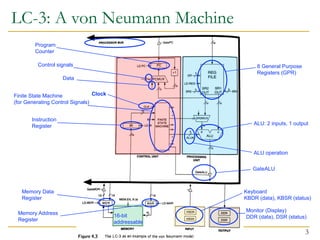
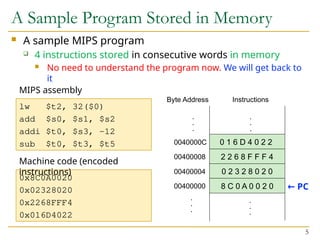
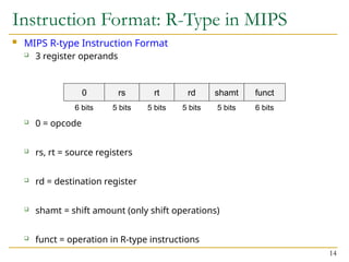
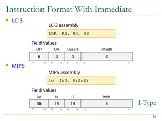
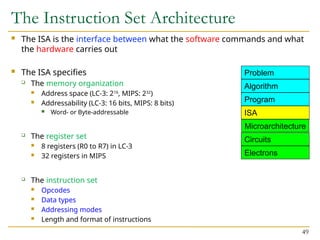
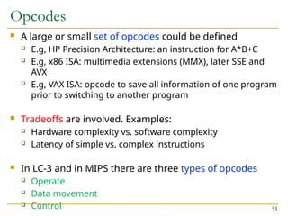
The document discusses the instruction set architecture (ISA) focusing on the von Neumann model as applied to LC-3 and MIPS, explaining how instructions are executed in a computer through an instruction cycle involving phases like fetch, decode, and execute. It covers types of instructions, formats, and the significance of opcodes and operands, detailing how high-level code translates into machine code. The document also compares the architectural features of LC-3 and MIPS, highlighting differences in register counts, addressability, and opcode usage.
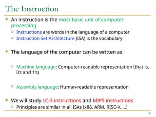
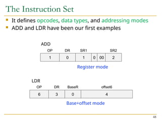
![The Instruction: Opcode & Operands
An instruction is made up of two parts
Opcode and Operands
Opcode specifies what the instruction does
Operands specify who the instruction is to do it to
Both are specified in instruction format (or instr.
encoding)
An LC-3 instruction consists of 16 bits (bits [15:0])
Bits [15:12] specify the opcode 16 distinct opcodes in LC-
3
Bits [11:0] are used to figure out where the operands are
7](https://image.slidesharecdn.com/lec14-instructionsetarchitecture-241229104403-8549b667/85/Lec-14-Instruction-Set-Architecture-pptx-7-320.jpg)
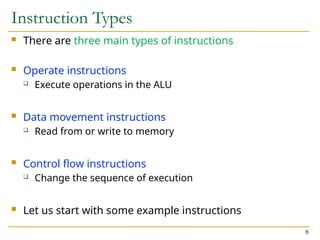
![Reading Word-Addressable Memory
Load word
load: mnemonic to indicate the load word operation
A: base address
i: offset
E.g., immediate or literal (a constant)
a: destination operand
Semantics: a Memory[A + i]
← 16
a = A[i]; load a, A, i
High-level code Assembly](https://image.slidesharecdn.com/lec14-instructionsetarchitecture-241229104403-8549b667/85/Lec-14-Instruction-Set-Architecture-pptx-16-320.jpg)
![Load Word in LC-3 and MIPS
LC-3 assembly
MIPS assembly (assuming word-addressable)
17
a = A[2]; LDR R3, R0, #2
High-level code LC-3 assembly
R3 Memory[R0 + 2]
←
a = A[2]; lw $s3, 2($s0)
High-level code MIPS assembly
$s3 Memory[$s0 + 2]
←
These instructions use a particular addressing mode
(i.e., the way the address is calculated), called base+offset](https://image.slidesharecdn.com/lec14-instructionsetarchitecture-241229104403-8549b667/85/Lec-14-Instruction-Set-Architecture-pptx-17-320.jpg)
![Load Word in Byte-Addressable MIPS
MIPS assembly
Byte address is calculated as: word_address *
bytes/word
4 bytes/word in MIPS
If LC-3 were byte-addressable (i.e., LC-3b), 2 bytes/word
18
a = A[2]; lw $s3, 8($s0)
High-level code MIPS assembly
$s3 Memory[$s0 + 8]
←](https://image.slidesharecdn.com/lec14-instructionsetarchitecture-241229104403-8549b667/85/Lec-14-Instruction-Set-Architecture-pptx-18-320.jpg)
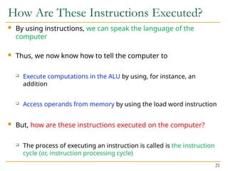
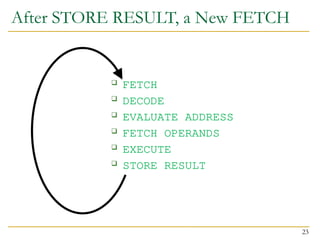
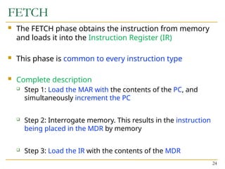
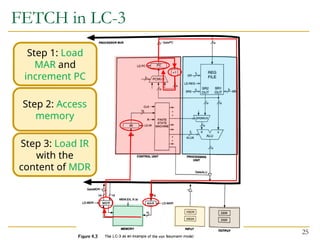
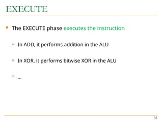
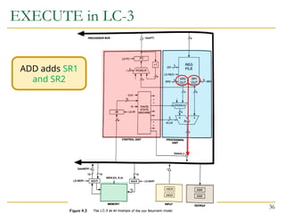
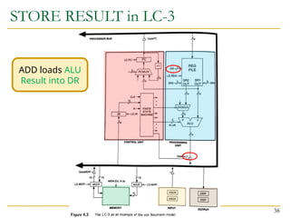
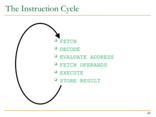
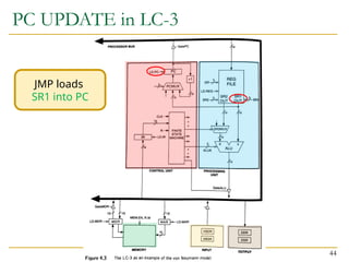
![The Instruction Cycle
The instruction cycle is a sequence of steps or phases, that an
instruction goes through to be executed
FETCH
DECODE
EVALUATE ADDRESS
FETCH OPERANDS
EXECUTE
STORE RESULT
Not all instructions require the six phases
LDR does not require EXECUTE
ADD does not require EVALUATE ADDRESS
Intel x86 instruction ADD [eax], edx is an example of instruction with
six phases
22](https://image.slidesharecdn.com/lec14-instructionsetarchitecture-241229104403-8549b667/85/Lec-14-Instruction-Set-Architecture-pptx-22-320.jpg)
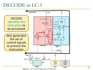
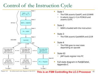
![DECODE
The DECODE phase identifies the instruction
Also generates the set of control signals to process the
identified instruction in later phases of the instruction
cycle
Recall the decoder (from Lecture 5)
A 4-to-16 decoder identifies which of the 16 opcodes is
going to be processed
The input is the four bits IR[15:12]
The remaining 12 bits identify what else is needed to
process the instruction 26](https://image.slidesharecdn.com/lec14-instructionsetarchitecture-241229104403-8549b667/85/Lec-14-Instruction-Set-Architecture-pptx-26-320.jpg)
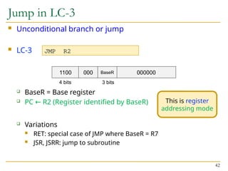
![Jump in MIPS
Unconditional branch or jump
MIPS
2 = opcode
target = target address
PC PC
← ✝
[31:28] | sign-extend(target) * 4
Variations
jal: jump and link (function calls)
jr: jump register
43
2 target
6 bits 26 bits
j target
J-Type
jr $s0
j uses pseudo-
direct addressing
mode
✝
This is the incremented PC
jr uses register
addressing mode](https://image.slidesharecdn.com/lec14-instructionsetarchitecture-241229104403-8549b667/85/Lec-14-Instruction-Set-Architecture-pptx-43-320.jpg)


![[DSC Europe 25] Borko Kozomora - Optimizing business workflows with advances ...](https://cdn.slidesharecdn.com/ss_thumbnails/hbgekyb0txw0xpo4yfml-borko-kozomora-leading-ai-transformation-260122103838-cc29ee38-thumbnail.jpg?width=640&height=640&fit=bounds)


