This paper discusses advancements in chronically implantable electrocorticography (ECoG) interfaces, highlighting a novel modular system utilizing an encapsulated neural interfacing acquisition chip (ENIAC) that offers improved spatiotemporal resolution and wide area coverage for brain monitoring. ECoG presents a minimally invasive alternative to EEG and penetrating electrodes, addressing limitations in resolution and long-term reliability. The authors explore challenges and solutions related to the design of next-generation ECoG systems, including recording, miniaturization, and wireless communication.

![ing [1], [2]. These advanced neurotechnologies will enable
new studies and experiments to augment our current under-
standing of the brain, thereby enabling tremendous advances
in diagnosis and treatment opportunities over a broad range
of neurological diseases and disorders.
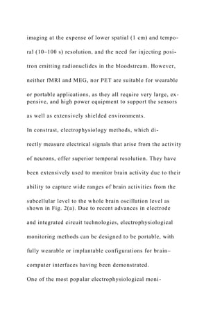
Studying the dynamics and connectivity of the brain
requires a wide range of technologies to address multiple
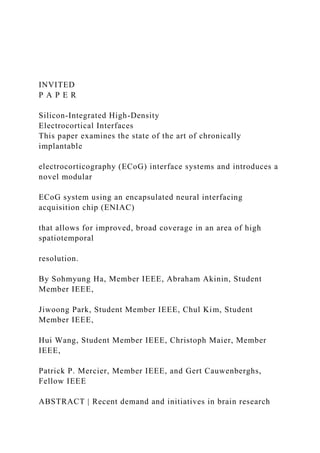
temporal and spatial scales. Fig. 1 shows spatial and tem-
poral resolutions and spatial coverage of the various brain
monitoring methods that are currently available [3]–[6].
Noninvasive methods such as magnetic resonance im-
aging (MRI), functional magnetic resonance imaging
Manuscript received January 1, 2016; revised May 24, 2016;
accepted May 30, 2016.
Date of publication August 5, 2016; date of current version
December 20, 2016. This
work was supported by the University of California
Multicampus Research Programs
and Initiatives (MRPI) and the University of California San
Diego Center for Brain
Activity Mapping.
The authors are with the University of California San Diego, La
Jolla, CA 92093-0412
USA (e-mail: [email protected]; [email protected];
[email protected]).](https://image.slidesharecdn.com/invitedpapersilicon-integratedhigh-densityelectro-221018173726-0381cdf9/85/INVITEDP-A-P-E-RSilicon-Integrated-High-DensityElectro-docx-4-320.jpg)
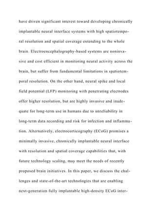
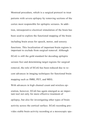
![toring methods is electroencephalography (EEG), which
records electrical activity on the scalp resulting from
volume conduction of coherent collective neural activity
throughout the brain, as illustrated in Fig. 2(a). EEG re-
cording is safe (noninvasive) and relatively inexpensive,
but its spatiotemporal resolution is limited to about 1 cm
and 100 Hz, due largely to the dispersive electrical prop-
erties of several layers of high-resistive tissue, particu-
larly skull, between the brain and the scalp. In contrast,
recording with intracranial brain-penetrating microelec-
trodes [labeled as EAP + LFP in Fig. 2(a)] can achieve
much higher resolution due to the much closer proximity
to individual neurons. Thus, it is also widely used
for brain research and brain–computer interface (BCI)
applications. Using microelectrodes, extracellular action
potential (EAPs) and local field potentials (LFPs) can be
recorded from multiple neurons across multiple cortical
areas and layers. Even though penetrating microelec-
trodes can provide rich information from neurons, they](https://image.slidesharecdn.com/invitedpapersilicon-integratedhigh-densityelectro-221018173726-0381cdf9/85/INVITEDP-A-P-E-RSilicon-Integrated-High-DensityElectro-docx-7-320.jpg)
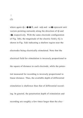
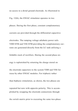
![can suffer from tissue damage during insertion [7]–[9],
Fig. 1. Spatial and temporal resolution as well as spatial
coverage
of various neural activity monitoring modalities [3]–[5]. For
each
modality shown, the lower boundary of the box specifies the
spatial resolution indicated on the left axis, whereas the upper
boundary specifies the spatial coverage on the right axis. The
width of each box indicates the typical achievable range of
temporal resolution. Portable modalities are shown in color.
Bridging an important gap between noninvasive and highly
invasive techniques, �ECoG has emerged as a useful tool for
diagnostics and brain-mapping research.
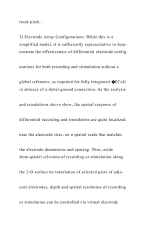
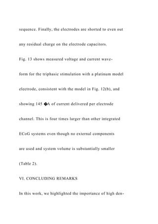
Fig. 2. (a) Conventional electrophysiology methods including
EEG,
ECoG, and neural spike and LFP recording with penetrating
microelectrodes. Both EEG and ECoG can capture correlated
collective volume conductions in gyri such as regions of a-b, d-
e,
and j-k. However, they cannot record opposing volume
conductions in sulci such as regions of b-c-d and e-f-g and](https://image.slidesharecdn.com/invitedpapersilicon-integratedhigh-densityelectro-221018173726-0381cdf9/85/INVITEDP-A-P-E-RSilicon-Integrated-High-DensityElectro-docx-8-320.jpg)
![random dipole layers such as regions of g-h and l-m-n-o [18].
(b) Emerging fully implantable �ECoG technologies enabled by
flexible substrate ECoG microarrays and modular ECoG
interface
microsystems. Such technologies are capable of capturing local
volume conducting activities missed by conventional methods,
and are extendable to cover large surface area across cortex.
12 Proceedings of the IEEE | Vol. 105, No. 1, January 2017
Ha et al.: Silicon-Integrated High-Density Electrocortical
Interfaces
Authorized licensed use limited to: University of Houston.
Downloaded on March 25,2020 at 04:55:14 UTC from IEEE
Xplore. Restrictions apply.
and have substantial limitations in long-term chronic
applications due to their susceptibility to signal degrada-
tion from electrode displacement and immune response
against the electrodes [10]. Because of the more extreme
invasiveness and longevity issues, chronic implantation
of penetrating microelectrodes in humans is not yet
viable.](https://image.slidesharecdn.com/invitedpapersilicon-integratedhigh-densityelectro-221018173726-0381cdf9/85/INVITEDP-A-P-E-RSilicon-Integrated-High-DensityElectro-docx-9-320.jpg)
![Between the two extremes of EEG and penetrating
microelectrode arrays, a practical alternative technique is
electrocoticography (ECoG), or intracranial/intraoperative
EEG (iEEG), which records synchronized postsynaptic po-
tentials at locations much closer to the cortical surface, as
illustrated in Fig. 2(a). Compared to EEG, ECoG has high-
er spatial resolution [11]–[13], higher signal-to-noise ratio,
broader bandwidth [14], and much less susceptibility to ar-
tifacts from movement, electromyogram (EMG), or elec-
trooculargram (EOG) [15], [16]. In addition, ECoG does
not penetrate the cortex, does not scar, and can have supe-
rior long-term signal stability recording through subdural
surface electrodes.
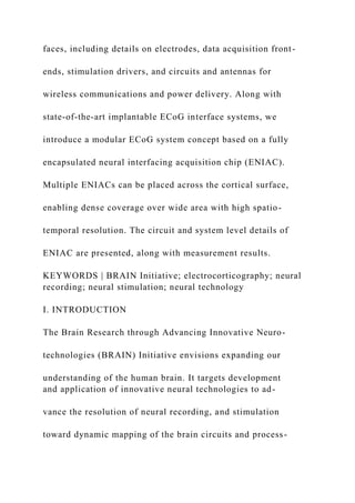
ECoG recording was pioneered in the 1920s by
Hans Berger [17]. He recorded ECoG signals with elec-
trodes placed on the dural surface of human patients.
In the 1930s through 1950s, Wilder Penfield and
Herbert Jasper at the Montreal Neurological Institute
used ECoG to identify epileptogenic zones as a part of the](https://image.slidesharecdn.com/invitedpapersilicon-integratedhigh-densityelectro-221018173726-0381cdf9/85/INVITEDP-A-P-E-RSilicon-Integrated-High-DensityElectro-docx-10-320.jpg)
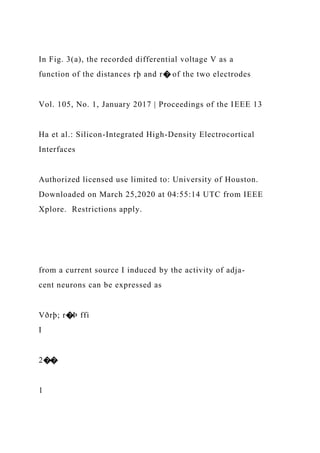
![static electric field equations with conductivities of tissue
layers are a good approximate representation [19]. To
first order, a volume conducting current monopole I
spreads radially through tissue with an outward current
density of magnitude I=4�r2 at distance r, giving rise to
an outward electric field of magnitude I=4��r2 and a
corresponding electrical potential I=4��r, where � is the
tissue volume conductivity.
1) Differential Recording: For EEG, a current dipole as
a closely spaced pair of opposing current monopoles is
typically an adequate model representing distant sources
of synchronous electrical activity across large assemblies
of neurons or synapses [19]. In contrast, for implanted
neural recording including ECoG and single-unit neural
spike/LFP recording, a set of monopole currents result-
ing from individual neural units is a more appropriate](https://image.slidesharecdn.com/invitedpapersilicon-integratedhigh-densityelectro-221018173726-0381cdf9/85/INVITEDP-A-P-E-RSilicon-Integrated-High-DensityElectro-docx-14-320.jpg)


![Ha et al.: Silicon-Integrated High-Density Electrocortical
Interfaces
Authorized licensed use limited to: University of Houston.
Downloaded on March 25,2020 at 04:55:14 UTC from IEEE
Xplore. Restrictions apply.
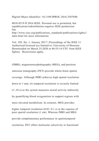
B. Electrode Interfaces for ECoG
Electrodes, which couple ECoG signals from the brain
into the analog front-end (AFE) amplifiers, are the first
interface to ECoG systems. Thus, their properties,
including materials, geometries, and placement are of
crucial importance in building entire acquisition and
actuation systems [32].
Given the distance between the scalp and individual
neuronal current sources and sinks, EEG recording is un-](https://image.slidesharecdn.com/invitedpapersilicon-integratedhigh-densityelectro-221018173726-0381cdf9/85/INVITEDP-A-P-E-RSilicon-Integrated-High-DensityElectro-docx-23-320.jpg)
![suitable for detecting small local field potentials as
shown in Fig. 2(a). Electrical dipole signals travel a mini-
mum distance of 1 cm between the outer surface of the
cerebral cortex to the scalp, including layers of cerebro-
spinal fluid, meninges, bone and skin, all with varying
electrical properties. Through this path the effect of a
small-localized dipole source is not only greatly attenu-
ated but also spatially averaged among a myriad of neigh-
bors, resulting in practical and theoretical limits to the
spatiotemporal resolution of EEG [33]. As implied in (1),
centimeter-sized electrode arrays with centimeter spac-
ings in conventional ECoG recordings are better than
EEG, but have limitations in resolving current sources of
neural activity of size smaller than the electrode pitch. A](https://image.slidesharecdn.com/invitedpapersilicon-integratedhigh-densityelectro-221018173726-0381cdf9/85/INVITEDP-A-P-E-RSilicon-Integrated-High-DensityElectro-docx-24-320.jpg)
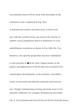
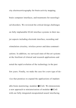
![(a) Example of a conventional electrode array placed on the
subdural
cortex (top) with post-operative radiograph showing electrode
array placement (bottom). The pitch and diameter of electrodes
are
1 cm and 2 mm, respectively [20]. (b) �ECoG electrode array
placed along with a conventional ECoG electrode array [21],
[22].
(c) Patient-specific electrode array for sulcal and gyral
placement [23]. (d) Flexible 252-channel ECoG electrode array
on a thin
polyimide foil substrate [24]. (e) �ECoG electrode array with
124 circular electrodes with three different diameters [25].
(f) Parylene-coated metal tracks and electrodes within a silicone
rubber substrate [26]. (g) A transparent �ECoG electrode array
with
platinum electrodes on a Parylene C substrate [27]. (h) An
electrode array with poly (3, 4-ethylenedioxythiophene) (PDOT)
and](https://image.slidesharecdn.com/invitedpapersilicon-integratedhigh-densityelectro-221018173726-0381cdf9/85/INVITEDP-A-P-E-RSilicon-Integrated-High-DensityElectro-docx-26-320.jpg)
![PEDOT-carbon nanotube (CNT) composite coatings for lower
electrode interface impedance [28]. (i) A flexible electrode
array on a
bioresorbable substrates of silk fibroin [29]. (j) Flexible active
electrode array with two integrated transistors on each pixel for
ECoG
signal buffering and column multiplexing for high channel
count [30]. (k) Flexible ECoG array with embedded light-
emitting diodes
for optogenetics-based stimulation [31].
Vol. 105, No. 1, January 2017 | Proceedings of the IEEE 15
Ha et al.: Silicon-Integrated High-Density Electrocortical
Interfaces
Authorized licensed use limited to: University of Houston.
Downloaded on March 25,2020 at 04:55:14 UTC from IEEE
Xplore. Restrictions apply.](https://image.slidesharecdn.com/invitedpapersilicon-integratedhigh-densityelectro-221018173726-0381cdf9/85/INVITEDP-A-P-E-RSilicon-Integrated-High-DensityElectro-docx-27-320.jpg)
![in G 1 mm pitch arrays have very high impedance, which
results in poor signal quality, and reduced charge trans-
fer capacity, which typically reduces stimulation effi-
ciency. Such limitations have been addressed by
micropatterning increased surface area, and carbon nano-
tube [34] or conductive polymer coatings [Fig. 4(h)]
[28]. Flexible substrates have also reduced the effective
distance between source and electrodes through tight,
conformal geometries [24], [26]. Aside from creating
ultraflexible thin materials, dissolvable substrates leave
behind a mesh of thin unobtrusive wires and electrodes
with a superior curved conformation and biocompatibil-
ity as shown in Fig. 4(i) [29], [35].
Even with advances in flexible electrode arrays, the](https://image.slidesharecdn.com/invitedpapersilicon-integratedhigh-densityelectro-221018173726-0381cdf9/85/INVITEDP-A-P-E-RSilicon-Integrated-High-DensityElectro-docx-28-320.jpg)
![number of channels in practical systems is still limited to
approximately 100 because of the high density of intercon-
nections between electrode arrays and corresponding
acquisition systems. Active electrodes are an emerging
approach to maximize number of electrode channels while
maintaining a small number of wired connections to the
electrode array. Advanced fabrication techniques can pro-
duce arrays of electrodes with direct integration of transis-
tors on the flexible substrate as shown in Fig. 4(j) [30] This
approach can be supplemented with additional in situ
devices capable of multiplexing several hundreds of record-
ing channels, thereby reducing the required number of
wires and interconnections. Another emergent approach](https://image.slidesharecdn.com/invitedpapersilicon-integratedhigh-densityelectro-221018173726-0381cdf9/85/INVITEDP-A-P-E-RSilicon-Integrated-High-DensityElectro-docx-29-320.jpg)
![combining active recording electrodes and new polymeric
materials has led to the development of organic electro-
chemical transistors in ECoG arrays [36]. However, one
limitation of current active arrays is that the same elec-
trode cannot be used for stimulation. Recently, transparent
electrode arrays with integrated light path for simulta-
neous ECoG recording and optogenetic stimulation have
been demonstrated as shown in Fig. 4(k) [31]. The active
development of novel electrode interfaces has not only im-
proved conventional ECoG recording, but also generated
new applications and therapeutic opportunities.
C. Integrated Circuit Interfaces for
Data Acquisition
Neural data acquisition with a high spatial resolution](https://image.slidesharecdn.com/invitedpapersilicon-integratedhigh-densityelectro-221018173726-0381cdf9/85/INVITEDP-A-P-E-RSilicon-Integrated-High-DensityElectro-docx-30-320.jpg)
![quire higher communication throughput, increasing the
power consumption of communication. All these require-
ments are interrelated and trade off with each other in
many ways, as indicated in Table 1 [32], [37], [38].
The noise-current tradeoff in instrumentation ampli-
fiers (IAs) is well represented by the noise efficiency
factor (NEF), which is expressed as
NEF ¼ Vrms;in
ffiffiffiffiffiffiffiffiffiffiffiffiffiffiffiffiffiffiffiffiffiffiffiffiffiffi
ffiffi
2Itot
�Vt � 4kT � BW
r
(3)
where Vrms;in is the total input-referred noise, Itot the](https://image.slidesharecdn.com/invitedpapersilicon-integratedhigh-densityelectro-221018173726-0381cdf9/85/INVITEDP-A-P-E-RSilicon-Integrated-High-DensityElectro-docx-33-320.jpg)
![total current drain, Vt the thermal voltage, and BW the
3-dB bandwidth of the system [39]. To minimize noise
with a given current consumption or minimize current
consumption with a upper-bound noise limit, various
Table 1 Design Factors and Tradeoffs in Integrated ECoG
Interfaces
16 Proceedings of the IEEE | Vol. 105, No. 1, January 2017
Ha et al.: Silicon-Integrated High-Density Electrocortical
Interfaces
Authorized licensed use limited to: University of Houston.
Downloaded on March 25,2020 at 04:55:14 UTC from IEEE
Xplore. Restrictions apply.
design techniques have been proposed and demonstrated
to address this challenges [40]–[59]. Such techniques to
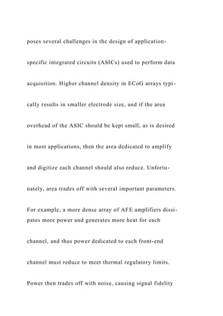
minimize NEF include 1) utilizing the weak inversion re-](https://image.slidesharecdn.com/invitedpapersilicon-integratedhigh-densityelectro-221018173726-0381cdf9/85/INVITEDP-A-P-E-RSilicon-Integrated-High-DensityElectro-docx-34-320.jpg)
![gion of CMOS operation to maximize transconductance
efficiency [37], [40], [60], [61]; 2) chopper stabilization
techniques to reduce 1=f noise and other low-frequency
noise [41], [43], [45], [47], [48], [62], [63]; 3) dynamic
range manipulation to reduce power supply voltages
[54], [55] using spectrum-equalizing AFE [64], [65]; and
4) using current-reusing nMOS and pMOS input pairs to
maximize transconductance and achieve an NEF below
two [54], [56]–[59] (Fig. 5).
Challenges in meeting the other specifications listed
in Table 1 have also been addressed using various cir-
cuit techniques. For example, several dc-coupling IAs
have been demonstrated in order to avoid external ac-](https://image.slidesharecdn.com/invitedpapersilicon-integratedhigh-densityelectro-221018173726-0381cdf9/85/INVITEDP-A-P-E-RSilicon-Integrated-High-DensityElectro-docx-35-320.jpg)
![coupling capacitors at the input of the AFE [42], [43].
In these designs, electrode offsets are canceled by feed-
back currents via a dc-servo loop [42], [43] or by capac-
itive feedback [66].
Integration of higher channel count on a single
chip has been pursued, as well. Thus far, chips with
approximately 100–300 data acquisition channels have
been reported [54], [67]–[70]. One of the strategies
to reduce area and power consumption in order to
maximize channel density is the use of scaled pro-
cesses such as 65-nm complementary metal–oxide–
semiconductor (CMOS) [66], achieving 64 channels
with a silicon area of 0.025 mm
2
per channel. For high-](https://image.slidesharecdn.com/invitedpapersilicon-integratedhigh-densityelectro-221018173726-0381cdf9/85/INVITEDP-A-P-E-RSilicon-Integrated-High-DensityElectro-docx-36-320.jpg)
![er density, in some designs, a SAR ADC is shared by
about 8–16 AFEs using a time multiplexer [54]. In doing
so, power-efficient multiplexers [71] and time-interleaving
sample-and-hold circuits in SAR ADCs have been demon-
strated. Alternatively, a dedicated ADC per AFE channel
has been also pursued due to its ease of integration with a
larger number of channels [44], [66].
D. Integrated Circuit Interfaces for Stimulation
Historically, electrical stimulation on the cortical sur-
face was pioneered by Penfield [72] as intraoperative
planning for epileptic patients, demonstrating the local-
ized function of different regions of the cortex [73].
Since then, functional neural stimulation has been exten-
sively investigated and developed during the past de-](https://image.slidesharecdn.com/invitedpapersilicon-integratedhigh-densityelectro-221018173726-0381cdf9/85/INVITEDP-A-P-E-RSilicon-Integrated-High-DensityElectro-docx-37-320.jpg)
![cades, making great progress for various clinical
applications such as deep brain stimulation, cochlear im-
plants, cardiac pacemakers, bladder control implants,
and retinal prostheses. Given that many epilepsy patients
already require implantation of ECoG monitoring instru-
mentation, there is a great opportunity for closed-loop
electrical control of seizure activity at much higher reso-
lution and precision than transcranial electric [74] and
transcranial magnetic stimulation [75], [76]. These em-
bedded stimulators would not require any additional in-
vasive risks, and could potentially prevent more drastic
treatments such as partial removal of the cortex. An
implantable recording and stimulation system can con-](https://image.slidesharecdn.com/invitedpapersilicon-integratedhigh-densityelectro-221018173726-0381cdf9/85/INVITEDP-A-P-E-RSilicon-Integrated-High-DensityElectro-docx-38-320.jpg)
![tain a digital signal processor capable of deciding when
to stimulate [77]. Other applications of cortical stimula-
tion include closed-loop brain computer interfaces (BCI)
which aim to generate functional maps of the brain [78],
restore somatosensory feedback [76], restore motor con-
trol to tetraplegics [79], aid stroke survivors [80], [81],
restore vision [82], reduce pain [73], or even change
emotional state [83].
Pushing the form factor and channel density of the
neural interface systems to the limit requires addressing
several challenges in ASICs for stimulation. Smaller form
factor and higher channel density require smaller elec-
trode size, which limits charge transfer capacity for](https://image.slidesharecdn.com/invitedpapersilicon-integratedhigh-densityelectro-221018173726-0381cdf9/85/INVITEDP-A-P-E-RSilicon-Integrated-High-DensityElectro-docx-39-320.jpg)
![effective stimulation. Hence, higher voltage rails of more
than �10 V and/or high-voltage processes are required
typically [84]–[86], in turn this results in higher power
consumption, larger silicon area, and system complexity
to generate and handle high-voltage signals. Instead of
maintaining a constant high-voltage power supply, some
designs save power by generating a large power rail only
when actively stimulating [77], [87], [88].
For further power savings, adiabatic stimulation has
been also actively investigated. Adiabatic stimulators gen-
erate ramping power rails that closely follow the voltages
at the stimulation electrode, minimizing unnecessary
voltage drops across the current source employed for
conventional constant-current stimulation. Various](https://image.slidesharecdn.com/invitedpapersilicon-integratedhigh-densityelectro-221018173726-0381cdf9/85/INVITEDP-A-P-E-RSilicon-Integrated-High-DensityElectro-docx-40-320.jpg)
![designs have been implemented with external capacitors
[89], external inductors [90], and charge pumps [87].
Still, there is much room for improvement in the imple-
mentation of adiabatic stimulators in fully integrated,
miniaturized implantable ICs.
It is generally desired to minimize the area occupied
per stimulation channel for high-density integration.
To date, integration of 100–1600 channels has been
Fig. 5. Noise efficiency factors of state-of-the-art
instrumentation amplifiers for biopotential recording
applications.
Vol. 105, No. 1, January 2017 | Proceedings of the IEEE 17
Ha et al.: Silicon-Integrated High-Density Electrocortical
Interfaces](https://image.slidesharecdn.com/invitedpapersilicon-integratedhigh-densityelectro-221018173726-0381cdf9/85/INVITEDP-A-P-E-RSilicon-Integrated-High-DensityElectro-docx-41-320.jpg)
![Authorized licensed use limited to: University of Houston.
Downloaded on March 25,2020 at 04:55:14 UTC from IEEE
Xplore. Restrictions apply.
achieved [84]–[86], [91]–[93]. In order to integrate such
high channel counts, programmability of waveform pa-
rameters, individual connectivity to each channel, and/or
charge balancing need to be compromised to some ex-
tent. For example, groups of 4–8 electrodes in [91],
[93]–[95] can share a single digital-to-analog converter
for optimized, high density integration.
Safety is of the utmost importance in chronic neural
interfaces, so charge balancing is imperative [96]. Resid-
ual dc results in tissue damage, production of toxic by-](https://image.slidesharecdn.com/invitedpapersilicon-integratedhigh-densityelectro-221018173726-0381cdf9/85/INVITEDP-A-P-E-RSilicon-Integrated-High-DensityElectro-docx-42-320.jpg)
![products, and electrode degradation [96]. However, it is
quite challenging to assure charge balance for each chan-
nel in high-channel neural interface systems. One of the
most straightforward strategies is to employ serial dc-
blocking capacitors, inherently forcing the net dc to be
zero all the time. This method has been employed for
neural stimulation applications [97]–[99] due to its in-
trinsic safety when area permits. However, the required
blocking capacitance is often prohibitively large for on-
chip integration, and is thus inadequate for high-density
and/or miniaturized implants. Instead of external capaci-
tors, capacitive electrodes made with high-k dielectric
coatings have been investigated for safe neural interfaces](https://image.slidesharecdn.com/invitedpapersilicon-integratedhigh-densityelectro-221018173726-0381cdf9/85/INVITEDP-A-P-E-RSilicon-Integrated-High-DensityElectro-docx-43-320.jpg)
![[88], [100], [101]. Several other techniques for better
charge balancing have been demonstrated: 1) shorting
electrodes to ground [102]; and 2) utilizing a discharging
resistor [94], active current balancing by feedback con-
trol [103], [104], generating additional balancing current
pulses by monitoring electrode voltages [105], and em-
bedded DAC calibration [93], [106].
E. Integrated Electrocortical Online Data
Processing
The integration of signal processing with neurophysi-
ological sensing and actuation enables real-time online
control strategies toward realizing adaptive, autonomous
closed-loop systems for remediation of neurological dis-
orders [107], [108]. Online signal processing of ECoG](https://image.slidesharecdn.com/invitedpapersilicon-integratedhigh-densityelectro-221018173726-0381cdf9/85/INVITEDP-A-P-E-RSilicon-Integrated-High-DensityElectro-docx-44-320.jpg)
![data has tremendous potential to improve patient out-
comes in diseases currently lacking therapy or requiring
resection of otherwise healthy neural tissue such as in-
tractable epilepsy. As one of the treatments for epilepsy,
functional neurostimulation in response to detected sei-
zures has been proved effective in reduction of seizures
[109], [110]. For real-time closed-loop therapeutics, on-
line automated seizure prediction and/or detection based
on ECoG or EEG recordings of epileptic patients is im-
perative [111]–[114], and their on-chip implementation
has been actively investigated and demonstrated utilizing
extraction and classification of various signal features
such as power spectral densities and wavelet coefficients](https://image.slidesharecdn.com/invitedpapersilicon-integratedhigh-densityelectro-221018173726-0381cdf9/85/INVITEDP-A-P-E-RSilicon-Integrated-High-DensityElectro-docx-45-320.jpg)
![[47], [77], [115]–[118].
In addition, ECoG has proven a powerful modality for
BCI applications owing to richer features present in the
higher resolution ECoG signals compared to surface EEG,
which can be harnessed to more precisely infer sensory
recognition, cognition, and motor function. Since ECoG-
based BCI systems widely utilize spectral power density
for their inputs [119], frequency band power extraction
techniques have been implemented immediately follow-
ing AFEs avoiding digitization and RF data transmission
of whole ECoG raw signals [120], [121].
Such on-chip real-time ECoG data processing offers
two distinct advantages over offline as well as online off-](https://image.slidesharecdn.com/invitedpapersilicon-integratedhigh-densityelectro-221018173726-0381cdf9/85/INVITEDP-A-P-E-RSilicon-Integrated-High-DensityElectro-docx-46-320.jpg)
![chip processing. First, constrains on data bandwidth and
power consumption on the implant can be largely re-
lieved. In many implementations, raw recorded data are
wirelessly streamed out and delivered to either a unit
worn on the top of the head, or directly to a local base
station such as a smartphone. The power of such ap-
proaches is typically proportional to the communication
distance. Thus, the overall power consumption of designs
that stream over long distances can be dominated by the
power of communication circuits [47]. In order to reduce
system-level power consumption, several on-chip data
processing techniques have been applied for EEG- and
ECoG-based BCI systems and epileptic seizure detection.
By doing so, power consumption of RF data transmission](https://image.slidesharecdn.com/invitedpapersilicon-integratedhigh-densityelectro-221018173726-0381cdf9/85/INVITEDP-A-P-E-RSilicon-Integrated-High-DensityElectro-docx-47-320.jpg)
![can be drastically reduced [47]. Second, local processing
may alleviate stringent latency and buffer memory
requirements in the uplink transmission of data for
external processing, especially where multiple implants
are time-multiplexed between a common base station.
III. SYSTEM CONSIDERATIONS
A. Powering
Major challenges in implantable medical devices
(IMDs) for high-density brain activity monitoring are
fundamentally posed by their target location. Some of
these IMDs can be wholly placed on the cortex within a
very limited geometry as shown in Fig. 2(b) In other
cases, only the electrode array is placed on the cortex](https://image.slidesharecdn.com/invitedpapersilicon-integratedhigh-densityelectro-221018173726-0381cdf9/85/INVITEDP-A-P-E-RSilicon-Integrated-High-DensityElectro-docx-48-320.jpg)
![while the other components can be located in the empty
space created by a craniotomy [122], or under the scalp
with lead wires connected [123], [124]. Regardless of
placement, this constrained environment poses a difficult
power challenge.
There are three primary methods for powering an
implanted device: employing a battery, harvesting en-
ergy from the environment, and delivering power
transcutaneously via a wireless power transmitter [125],
[126]. A natural first choice would be a battery, as
they have been extensively used in other implantable
applications such as pacemakers. While it makes sense
to use a battery in a pacing application, where the
power of the load circuit is small (microwatts) and a](https://image.slidesharecdn.com/invitedpapersilicon-integratedhigh-densityelectro-221018173726-0381cdf9/85/INVITEDP-A-P-E-RSilicon-Integrated-High-DensityElectro-docx-49-320.jpg)

![ever, the total deliverable power highly depends on the
geometry and makeup of the receiving transducer, along
with the implant depth and orientation.
Optical powering through transmission of infrared
light has a very short penetration depth of a few millime-
ters, limiting its utility to subcutaneous and very shallow
implant applications [130]–[132]. Ultrasound, on the
other hand, can penetrate much deeper into tissue, po-
tentially powering implants located on the cortical sur-
face. In fact, it has been demonstrated that ultrasound
can more efficiently power millimeter-scale devices im-
planted deep into soft tissues than electromagnetic ap-
proaches [133]. However, it has also been shown that
ultrasonic energy does not efficiently penetrate bone,](https://image.slidesharecdn.com/invitedpapersilicon-integratedhigh-densityelectro-221018173726-0381cdf9/85/INVITEDP-A-P-E-RSilicon-Integrated-High-DensityElectro-docx-53-320.jpg)
![limiting opportunities to directly power cortical implants
from outside the skull. To overcome this, researchers
have proposed two-tiered systems, where electromag-
netic energy is coupled through the skull, then converted
to acoustic energy via an intermediate transducer system,
and finally delivered to the miniaturized implant through
soft tissue [134]. However, in addition to nontrivial pack-
aging and transducer design challenges, this is likely only
a reasonable approach when the implant to be powered
is either very deep, or very small (submillimeter scale).
For these reasons, ultrasonic power delivery is not typi-
cally considered for ECoG systems.
The most popular transcutaneous power delivery ap-](https://image.slidesharecdn.com/invitedpapersilicon-integratedhigh-densityelectro-221018173726-0381cdf9/85/INVITEDP-A-P-E-RSilicon-Integrated-High-DensityElectro-docx-54-320.jpg)
![proach utilizes electromagnetics. For devices implanted
to a depth of a few centimeters, and that are on the
order of millimeter-to-centimeter in diameter, near- or
mid-field electromagnetic power transfer is generally
considered to be the most efficient and practical method
to power such devices. Near-field power transfer, which
operates at frequencies up to approximately 100 MHz for
typical implants, has been extensively used for cochlear
implants [135], retinal prostheses [86], [93], and various
research IMD systems [122], [136]–[139], and has been
investigated and characterized to maximize its usage and
power transfer efficiency for implants [140]–[145].
Most conventional designs operate in the near-field](https://image.slidesharecdn.com/invitedpapersilicon-integratedhigh-densityelectro-221018173726-0381cdf9/85/INVITEDP-A-P-E-RSilicon-Integrated-High-DensityElectro-docx-55-320.jpg)
![between 1 and 20 MHz, since it is well known that con-
ductivity (and hence losses) in tissue increase at higher
frequencies, as shown in Fig. 6. Operating at higher fre-
quencies, it was previously argued, would encounter
higher losses and thus be less efficient. In addition, gov-
ernmental regulatory agencies limit the amount of power
that can be dissipated in tissue for safety reasons—the
U.S. Federal Communications Commission (FCC) sets a
specific absorption rate (SAR) of less than 1.6 W/kg, for
example. For these reasons, conventional transcutaneous
power transfer links operate in the low-megahertz range,
often at the 6.78- and 13.56-MHz ISM bands [125],
[144], [145].
However, it is also well known that the quality factor](https://image.slidesharecdn.com/invitedpapersilicon-integratedhigh-densityelectro-221018173726-0381cdf9/85/INVITEDP-A-P-E-RSilicon-Integrated-High-DensityElectro-docx-56-320.jpg)
![and radiation resistance of electrically small coil anten-
nas increases with increasing frequency. Thus, miniatur-
ized implants, which have electrically small coils for
wireless power reception, tend to prefer to operate at
higher frequencies, at least in air. In biological tissues,
the tradeoff between coil design and tissue losses results
in an optimal frequency for wireless power transmission
where efficiency is maximized. For example, the induc-
tance of coils located on miniaturized, millimeter-scale
implants ranges from 10 to 100 nH [66], [88], [146],
[147]. To compensate for reduced magnetic flux through
the miniaturized receiving coil, the carrier frequency for
wireless power transfer should be increased, often into](https://image.slidesharecdn.com/invitedpapersilicon-integratedhigh-densityelectro-221018173726-0381cdf9/85/INVITEDP-A-P-E-RSilicon-Integrated-High-DensityElectro-docx-57-320.jpg)
![the hundreds of megahertz to single-digit gigahertz range
[66], [146]–[149]. These prior studies have demonstrated
that it is possible to efficiently deliver milliwatts of
power to small, implanted devices under regulatory
limits, and thus electromagnetic approaches are the pri-
mary means to deliver power to implanted ECoG
devices.
B. Wireless Data Communication
Implanted ECoG monitoring devices need to convey
the acquired data to the external world through wireless
communication. The information received by the exter-
nal base station can be monitored, processed, and used
by users and care takers for health monitoring, treat-](https://image.slidesharecdn.com/invitedpapersilicon-integratedhigh-densityelectro-221018173726-0381cdf9/85/INVITEDP-A-P-E-RSilicon-Integrated-High-DensityElectro-docx-58-320.jpg)

![munication technology. Due to the wide availability of
far-field radio products and a myriad of different infra-
structures (e.g., Bluetooth Low Energy, WiFi, etc.), far-
field radios can be quickly adopted for robust operation
[122]. However, even state-of-the-art low-power radios
consume 9 1 nJ/b [125], [164], which is order-of-
magnitude larger than what typical ECoG recording
IMDs require.
As an alternative far-field transmission method, im-
pulse radio ultrawideband (IR-UWB) transmission has
emerged recently due to its low power consumption in
the range of a few tens of picojoule per bit (pJ/b) [165]–
[167]. Avoiding generation of a carrier with an accurate
frequency, noncoherent IR-UWB transmitters generates](https://image.slidesharecdn.com/invitedpapersilicon-integratedhigh-densityelectro-221018173726-0381cdf9/85/INVITEDP-A-P-E-RSilicon-Integrated-High-DensityElectro-docx-61-320.jpg)
![short pulses with ON–OFF keying (OOK) or pulse posi-
tion modulation (PPM). Due to its high and wide fre-
quency range (3.1–10 GHz), data rates of more than
10 Mb/s with tens of picojoules per bit have been re-
ported. [168] In addition, antennas for this type of trans-
mission do not need to be large. However, there are a
couple of critical reasons against their usage for IMDs
[125]. Foremost, their peak transmission power is large
due to the inherently duty-cycled nature of IR-UWB
transmitters. Thus, while the average power may be low,
a large high-quality power supply with a large battery of
capacitor is required to supply large peak currents, which
may be prohibitively large for many ECoG applications.](https://image.slidesharecdn.com/invitedpapersilicon-integratedhigh-densityelectro-221018173726-0381cdf9/85/INVITEDP-A-P-E-RSilicon-Integrated-High-DensityElectro-docx-62-320.jpg)
![Moreover, since IR-UWB operates at very high frequency
over 3 GHz, tissue absorption rate is higher.
In contrast to far-field communication methods, near-
field radios operate over short distances, typically within
one wavelength of the carrier frequency, and are thus
suitable for use when an external device is located di-
rectly on the head. In fact, since this configuration is
naturally present in wirelessly powered devices, near-
field communication can easily be implemented along
with this wireless powering. One of the most popular
data communication methods that can be implemented
along with forward power delivery is the backscattering
method [169]–[173]. This method modulates the load](https://image.slidesharecdn.com/invitedpapersilicon-integratedhigh-densityelectro-221018173726-0381cdf9/85/INVITEDP-A-P-E-RSilicon-Integrated-High-DensityElectro-docx-63-320.jpg)
![conditions of forward powering signals, and reflecting
this energy back to the interrogator. Since only a single
switch needs to be driven, the power consumed on the
Fig. 6. (a) Relative permittivity and specific conductivity over
frequency range from 10 to 100 GHz with most popular
frequency communication bands for ECoG implants [127],
[128].
(b) Relative permittivity and (c) specific conductivity of various
kinds of tissues including skin, fat, skull, CSF, gray and white
matter [129].
20 Proceedings of the IEEE | Vol. 105, No. 1, January 2017
Ha et al.: Silicon-Integrated High-Density Electrocortical
Interfaces
Authorized licensed use limited to: University of Houston.
Downloaded on March 25,2020 at 04:55:14 UTC from IEEE](https://image.slidesharecdn.com/invitedpapersilicon-integratedhigh-densityelectro-221018173726-0381cdf9/85/INVITEDP-A-P-E-RSilicon-Integrated-High-DensityElectro-docx-64-320.jpg)
![Xplore. Restrictions apply.
implant side is minimal, as carrier generation and active
driving of an antenna are not required. Since, with this
technology, a few picojoules per bit to tens of picojoules
per bit can be achieved [173], it has been widely adopted
by various IMDs [66], [86], [174]–[178]. However, exter-
nal data reception in backscattering systems can be
challenging in some cases because of the large power dif-
ference between the large power carrier signal and the
weak backscattered signal.
Forward telemetry for neural recording IMDs is typi-
cally used for sending configuration bits to the implant,
requiring a relatively low data rate typically much less](https://image.slidesharecdn.com/invitedpapersilicon-integratedhigh-densityelectro-221018173726-0381cdf9/85/INVITEDP-A-P-E-RSilicon-Integrated-High-DensityElectro-docx-65-320.jpg)
![than 100 kb/s. Hence, amplitude shift keying (ASK) has
been widely employed in such IMDs [88], [179], [180],
modulating the power carrier signals. For IMDs with
stimulation capability, forward telemetry for closed-loop
operation is typically time-multiplexed with backward
telemetry.
C. Hermetic Encapsulation
Implanted devices containing silicon ICs need pack-
aging in a protective enclosure to mitigate corrosion and
other contamination by surrounding electrolyte in the
body [181], [182]. Thus far, titanium-, glass- or ceramic-
based enclosures have been the primary means for
hermetic sealing in long-term implants, since these hard
materials have been shown to be biocompatible and](https://image.slidesharecdn.com/invitedpapersilicon-integratedhigh-densityelectro-221018173726-0381cdf9/85/INVITEDP-A-P-E-RSilicon-Integrated-High-DensityElectro-docx-66-320.jpg)
![impermeable to water [181]. Even though such hard en-
closures are used in the majority of long-term implants
[6], [111], [122], [150]–[155], [159], [183], their very
large volume and weight, typically much larger than the
ICs and supporting components they contain, prohibits
their use in high-dimensional neural interfaces heavily
constrained by anatomical space such as retinal prosthe-
ses [184] and �ECoG arrays [30]. In addition, hard pack-
aging requires intricate methods for hermetic sealing of
feedthroughs to polymer insulated extensions of the im-
plant such as electrode array cabling, limiting the density
of electrode channels due to feedthrough channel spac-
ing requirements.](https://image.slidesharecdn.com/invitedpapersilicon-integratedhigh-densityelectro-221018173726-0381cdf9/85/INVITEDP-A-P-E-RSilicon-Integrated-High-DensityElectro-docx-67-320.jpg)
![To overcome these challenges, conformal coating of
integrated electronics with polymers such as polyimide,
silicone, and parylene-C have been investigated as
alternatives. They are superior over metal, glass, and
ceramic hard seals in miniaturization, flexibility, and
compatibility with the semiconductor process [185].
However, polymers are susceptible to degradation and
are not long-term impermeable to body fluids. While
polymer encapsulation has been used for relatively
simple and short-term (less than 1–2 years) implants,
substantial improvements are needed for viable solu-
tions to long-term hermetic encapsulation [182], [186].
Recent next-generation advances in miniaturized her-
metic sealing of silicon integrated circuits, such as](https://image.slidesharecdn.com/invitedpapersilicon-integratedhigh-densityelectro-221018173726-0381cdf9/85/INVITEDP-A-P-E-RSilicon-Integrated-High-DensityElectro-docx-68-320.jpg)
![multilayer multimaterial coating [187], and encapsula-
tion using liquid crystal polymers (LCPs) [185], are
promising developments toward highly miniaturized
implantable electronics for chronic clinical use. Fur-
thermore, recent advances in dissolvable flexible elec-
tronics [188], [189] offer alternatives to hermetic
encapsulation for acute applications without the need
for post-use surgical extraction.
IV. STATE-OF-THE-ART ECoG
INTERFACE SYSTEMS
Various types of implantable devices for ECoG interfaces
have been developed for clinical use and neuroscience
research. Their target applications include treatment of
neurological disorders and ECoG-based BCIs. Fig. 7 illus-](https://image.slidesharecdn.com/invitedpapersilicon-integratedhigh-densityelectro-221018173726-0381cdf9/85/INVITEDP-A-P-E-RSilicon-Integrated-High-DensityElectro-docx-69-320.jpg)
![trates several state-of-the-art ECoG interface systems for
clinical and research applications.
On the clinical side, implantable devices shown in
Fig. 7(a)–(c) have been developed mostly for use in
closed-loop treatment of intractable epilepsy as an alter-
native to tissue resection. These devices monitor ECoG
signals and deliver stimulation to the seizure foci in re-
sponse to epileptic seizure detection. The NeuroPace
RNS System, shown in Fig. 7(a), is the first such sys-
tem to receive FDA approval for closed-loop treatment
in epilepsy patients, proven effective to reduce the fre-
quency of partial-onset seizures in human clinical trials
[191], [192].](https://image.slidesharecdn.com/invitedpapersilicon-integratedhigh-densityelectro-221018173726-0381cdf9/85/INVITEDP-A-P-E-RSilicon-Integrated-High-DensityElectro-docx-70-320.jpg)
![nels, targeting long-term ECoG recording fully implanted
in human patients [122] as shown in Fig. 7(d). This active
IMD (AIMD) is fully covered by a 50-mm-diameter her-
metic housing made of silicone-coated titanium with a
silicone-platinum electrode array on the bottom side. Its
silicone over-molding is extended to include two anten-
nas for RF communication and wireless power transfer.
The housing fits inside of a 50-mm craniotomy, and its
upper surface is just below the skin, with the implant re-
placing the previously existing bone. Two 32-channel
ECoG recording ASICs [193] are implemented for ECoG
recording, and commercial off-the-shelf components are
employed for data processing, communication, power
management, etc., leading to relatively high power](https://image.slidesharecdn.com/invitedpapersilicon-integratedhigh-densityelectro-221018173726-0381cdf9/85/INVITEDP-A-P-E-RSilicon-Integrated-High-DensityElectro-docx-72-320.jpg)
![consumption—75 mW for 32 channels. Its operation and
Vol. 105, No. 1, January 2017 | Proceedings of the IEEE 21
Ha et al.: Silicon-Integrated High-Density Electrocortical
Interfaces
Authorized licensed use limited to: University of Houston.
Downloaded on March 25,2020 at 04:55:14 UTC from IEEE
Xplore. Restrictions apply.
biocompatibility has been evaluated in vivo in nonhuman
primates.
Another example is the BrainCon system with
16-channel ECoG recording and 8-channel stimulation
designed for chronic implanted use in closed-loop hu-
man BCI [158]. Shown in Fig. 7(e), this device consists](https://image.slidesharecdn.com/invitedpapersilicon-integratedhigh-densityelectro-221018173726-0381cdf9/85/INVITEDP-A-P-E-RSilicon-Integrated-High-DensityElectro-docx-73-320.jpg)
![of an ECoG electrode array and an electronic package
with a magnet, an inductive coil, and electronic compo-
nents for data acquisition, stimulation, and communica-
tion. Targeted for long-term recording and cortical
stimulation in human patients, it is enclosed in a her-
metic package with medical grade silicone rubber [156],
[157], and was validated in vivo for more than ten
months [158].
Further miniaturization and advances in functionality
have been pursued through integration of circuits for
ECoG recording, wireless powering, and wireless com-
munication as shown in Fig. 7(f)–(j). In addition, low-
cost ECoG interfaces shown in Fig. 7(k) for acute animal
research have been developed [163], as have ECoG inter-](https://image.slidesharecdn.com/invitedpapersilicon-integratedhigh-densityelectro-221018173726-0381cdf9/85/INVITEDP-A-P-E-RSilicon-Integrated-High-DensityElectro-docx-74-320.jpg)
![faces with transparent electrode arrays for compatibility
with optogenetic stimulation shown in Fig. 7(l) [27].
Each of these devices offers substantial advances in
wireless and integrated ECoG technology with improved
functionality and increased density and channel counts.
Yet, most rely on substantial cabling in connecting to the
array of electrodes, or at least a wired connection to a
distal ground as reference.
Fig. 7. State-of-the-art ECoG interfacing systems. (a)
NeuroPace RNS system [150], [151]. (b) NeuroVista seizure
advisory system [111],
[152], [153]. (c) The neural interface (NI) system of Medtronic
[154], [155]. (d) The Wireless Implantable Multi-channel
Acquisition
system for Generic Interface with NEurons (WIMAGINE) [122].
(e) BrainCon system for a general-purpose medical BCI [156]–](https://image.slidesharecdn.com/invitedpapersilicon-integratedhigh-densityelectro-221018173726-0381cdf9/85/INVITEDP-A-P-E-RSilicon-Integrated-High-DensityElectro-docx-75-320.jpg)
![[158].
(f) The Wireless Human ECoG-based Real-time BMI System
(W-HERBS) [6], [159]. (g) �ECoG recording system of Cortera
Neurotechnologies, Inc. [66], [160]. (h) A ECoG recording
system with bidirectional capacitive data Telemetry [161]. (i)
An ECoG
recording system with a carbon nanotube microelectrode array
and a corresponding IC [34]. (j) A wireless ECoG interface
system with
a 64-channel ECoG recording application-specific integrated
circuit (ASIC) [162]. (k) An 8-channel low-cost wireless neural
signal
acquisition system made with off-the-shelf components [163].
(l) �ECoG recording system with an electrode array fabricated
on a
transparent polymer for optogenetics-based stimulation [27].
22 Proceedings of the IEEE | Vol. 105, No. 1, January 2017](https://image.slidesharecdn.com/invitedpapersilicon-integratedhigh-densityelectro-221018173726-0381cdf9/85/INVITEDP-A-P-E-RSilicon-Integrated-High-DensityElectro-docx-76-320.jpg)
![Ha et al.: Silicon-Integrated High-Density Electrocortical
Interfaces
Authorized licensed use limited to: University of Houston.
Downloaded on March 25,2020 at 04:55:14 UTC from IEEE
Xplore. Restrictions apply.
V. FULLY INTEGRATED MODULAR
�ECoG RECORDING AND STIMULATION
A. Encapsulated Neural Interfacing Acquisition
Chip (ENIAC)
As highlighted above, most current state-of-the-art
ECoG ASICs rely on external components, such as flexi-
ble substrates, electrode arrays, and antennas [27], [30],
[66], [122], [156]–[158], [161], [162]. In doing so, inte-
gration of all the components into a complete system
requires special fabrication processes, and, importantly,](https://image.slidesharecdn.com/invitedpapersilicon-integratedhigh-densityelectro-221018173726-0381cdf9/85/INVITEDP-A-P-E-RSilicon-Integrated-High-DensityElectro-docx-77-320.jpg)
![ence and called for by several brain initiatives, such
limitations must be overcome.
Instead of separating the electrodes and the ASIC, a
promising approach that we present below is to integrate
everything on a single encapsulated neural interfacing
and acquisition chip (ENIAC), including electrodes, an-
tennas for power and data telemetry, and all other cir-
cuits and components [88]. Thus, no external wires,
substrates, batteries, or any other external components
are required. Complete encapsulation of the ENIAC with
a biocompatible material removes direct contact to tis-
sue, including the electrodes for recording and stimula-
tion. As such, the chip itself serves as a complete](https://image.slidesharecdn.com/invitedpapersilicon-integratedhigh-densityelectro-221018173726-0381cdf9/85/INVITEDP-A-P-E-RSilicon-Integrated-High-DensityElectro-docx-79-320.jpg)
![standalone neural interfacing system.
As shown in Fig. 8 the ENIAC is designed to be small
enough ð3 � 3 � 0:25 mm3Þ to be placed among the
folds and curves of the cortical surface [see Fig. 2(b)],
and to be implanted through small skull fissures. Hence
it offers greater coverage of the cortical surface while be-
ing much less obtrusive than other minimally invasive
ECoG approaches, permitting even insertion without sur-
gery. As seen in the block diagram in Fig. 8, the chip
contains an LC resonant tank, electrodes, recording
channels, stimulator, power management units, and bidi-
rectional communication circuits.
Its first prototype, fabricated in a 180-�m CMOS
silicon-on-insulator (SOI) process, is shown on the upper](https://image.slidesharecdn.com/invitedpapersilicon-integratedhigh-densityelectro-221018173726-0381cdf9/85/INVITEDP-A-P-E-RSilicon-Integrated-High-DensityElectro-docx-80-320.jpg)
![right side of Fig. 8. With two turns and 100-�m
Fig. 8. Encapsulated neural interfacing acquisition chip
(ENIAC) [88], [190]. (a) System diagram showing the fully
integrated
functionality of the ENIAC comprising on-chip antenna,
electrodes, and all the circuitry for power management,
communication, ECoG
recording and stimulation. No external components are needed,
and galvanic contact to surrounding tissue is completely
eliminated in
the fully encapsulated device. (b) Chip micrograph and
dimensions of the prototype ENIAC.
Vol. 105, No. 1, January 2017 | Proceedings of the IEEE 23
Ha et al.: Silicon-Integrated High-Density Electrocortical
Interfaces
Authorized licensed use limited to: University of Houston.
Downloaded on March 25,2020 at 04:55:14 UTC from IEEE
Xplore. Restrictions apply.](https://image.slidesharecdn.com/invitedpapersilicon-integratedhigh-densityelectro-221018173726-0381cdf9/85/INVITEDP-A-P-E-RSilicon-Integrated-High-DensityElectro-docx-81-320.jpg)
![thickness, the on-chip coil results in an inductance of
23.7 nH. The same single coil is shared for wireless
power transfer and bidirectional RF communication.
Sixteen electrodes, which can be individually configured
as recording or stimulating channels, are integrated di-
rectly on the top metal layer of the chip. To enhance en-
ergy efficiency and remove the need for separate
rectification and regulation stages, an integrated resonant
regulating rectifier IR3 [190] is implemented. In addition,
an adiabatic stimulator generates constant-current stimu-
lation pulses from the RF power input in an adiabatic
manner, much more energy efficient than conventional
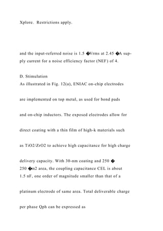
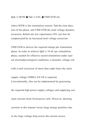
stimulation from dc static power supplies.](https://image.slidesharecdn.com/invitedpapersilicon-integratedhigh-densityelectro-221018173726-0381cdf9/85/INVITEDP-A-P-E-RSilicon-Integrated-High-DensityElectro-docx-82-320.jpg)

![limit (2 W/kg in IEEE std. 1528). Fig. 9(c) shows the maxi-
mum transmit power at the SAR limit, and corresponding
maximum deliverable power at the implant, for varying
distance of the air gap between the loop transmitter and
the scalp. The optimal distance for maximum power deliv-
ery, trading between reduced SAR-limited transmit power
at lower distance and increased path losses at higher dis-
tance [194], was found to be around 5 mm.
ENIAC minimizes power losses in the received power
from the RF coil owing to an integrated resonant regulat-
ing rectifier ðIR3Þ architecture that combines power
management stages of rectification, regulation, and dc
conversion, eliminating typical losses due to inefficien-
cies at each stage when implemented separately. As illus-](https://image.slidesharecdn.com/invitedpapersilicon-integratedhigh-densityelectro-221018173726-0381cdf9/85/INVITEDP-A-P-E-RSilicon-Integrated-High-DensityElectro-docx-84-320.jpg)
![trated in Fig. 10(a), IR3 generates a constant power
supply 0.8 V independent of fluctuation in the LC tank
voltages. IR3 operates by adapting both width and fre-
quency of pulsed rectifier switching based on a feedback
signal derived from VDD [190].
Concurrently, the amplitude-shift-keying (ASK) de-
modulator tracks and amplifies the envelope of the LC
tank voltages to decode transmitted configuration data as
illustrated on the bottom of Fig. 10(a). The ASK commu-
nication is used to wirelessly configure the operation
modes and parameters of the chip. To synchronize data
reception, a 16-b predetermined identification code is
used as prefix followed by serial peripheral interface
(SPI) signals.](https://image.slidesharecdn.com/invitedpapersilicon-integratedhigh-densityelectro-221018173726-0381cdf9/85/INVITEDP-A-P-E-RSilicon-Integrated-High-DensityElectro-docx-85-320.jpg)

![between the transmitter and the scalp, optimum around 5 mm.
Green arrows denote minimum path losses at each air distance.
24 Proceedings of the IEEE | Vol. 105, No. 1, January 2017
Ha et al.: Silicon-Integrated High-Density Electrocortical
Interfaces
Authorized licensed use limited to: University of Houston.
Downloaded on March 25,2020 at 04:55:14 UTC from IEEE
Xplore. Restrictions apply.
was placed 1 cm above the ENIAC. The top right panel
in Fig. 10(b) shows the measured coil voltages simulta-
neously rectified and regulated by the IR3 [190], [195]
to produce the supply voltage VDD � 0:8 V. The total
transmitted power is about 5 mW, of which around
80 �W is received by the ENIAC. The bottom panel](https://image.slidesharecdn.com/invitedpapersilicon-integratedhigh-densityelectro-221018173726-0381cdf9/85/INVITEDP-A-P-E-RSilicon-Integrated-High-DensityElectro-docx-87-320.jpg)
![capacitive division. Similar to differential recording across
a pair of adjacent electrodes (Section II-A1), the internal
common-mode reference VAVG allows single-ended record-
ing over all 16 electrodes without the need for a distal
external ground connection. A pMOS-based pseudoresis-
tor [in the inset of Fig. 11(a)] is used to set the dc oper-
ating point at VREF for the capacitive division to allow for
very high (T�-range) resistance in very small silicon area
[40], [196].
The first low-noise amplifier stage has a noninverting
configuration with a feedback capacitor C1 and a common-
mode coupling capacitor of 39 � C1, which connects to
the common-mode averaging node VAVG, resulting in a
differential voltage gain of 40 (V/V). VAVG is buffered
and used for common-mode rejection in the second AFE
stage. The second AFE stage provides variable gain by
manipulating the connections of two capacitors, con-](https://image.slidesharecdn.com/invitedpapersilicon-integratedhigh-densityelectro-221018173726-0381cdf9/85/INVITEDP-A-P-E-RSilicon-Integrated-High-DensityElectro-docx-89-320.jpg)
![nected either as input or as feedback capacitors [46],
[54]. Output signals of the AFEs are multiplexed and
buffered to the SAR ADC, which has time-interleaving
sample-and-hold input DACs to ensure longer sampling
time, leading to power saving in buffering the input
DAC of the ADC.
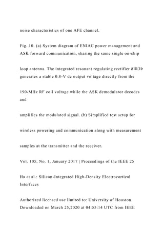
Measurement results for the AFE, characterizing its
frequency response and noise performance, are shown in
Fig. 11(b) and (c). Variable 50–70-dB gain is supported,
Fig. 11. (a) Circuit diagram of the recording module of ENIAC
with
16 AFE channels, 16:1 analog multiplexer (MUX), and
successive
approximation register (SAR) ADC. (b) Measured frequency
and](https://image.slidesharecdn.com/invitedpapersilicon-integratedhigh-densityelectro-221018173726-0381cdf9/85/INVITEDP-A-P-E-RSilicon-Integrated-High-DensityElectro-docx-90-320.jpg)
![Instead, a much better way to perform stimulation is
to slowly ramp up the supply rails in an adiabatic fashion
to minimize the voltage drop across the current source.
Generation of the adiabatic voltage rails can be imple-
mented in various ways. External capacitors [89] or an
external inductor [90] can be employed. Alternatively,
pulse width control in rectifier can be used [199]. How-
ever, all of these methods have output ranges within the
LC tank swing voltages or VDD. Recently, on-chip charge
pumps are employed to generate a wide voltage excur-
sion for adiabatic stimulation [87]. Because this approach
utilizes the dc power supply as the input of charge
pumps, series of power efficiency loss cannot be avoided
in implantation settings. In addition, this method could](https://image.slidesharecdn.com/invitedpapersilicon-integratedhigh-densityelectro-221018173726-0381cdf9/85/INVITEDP-A-P-E-RSilicon-Integrated-High-DensityElectro-docx-94-320.jpg)
![Authorized licensed use limited to: University of Houston.
Downloaded on March 25,2020 at 04:55:14 UTC from IEEE
Xplore. Restrictions apply.
Acknowledgment
The authors would like to thank V. Gilja, S. Dayeh,
E. Halgren, B. McNaughton, and J. Viventi for critical
input and stimulating discussions on clinical and funda-
mental neuroscience applications of high-density ECoG
neural interfaces.
REFERENCES
[1] The White House, “The BRAIN Initiative.”
[Online]. Available: https://www.
whitehouse.gov/BRAIN](https://image.slidesharecdn.com/invitedpapersilicon-integratedhigh-densityelectro-221018173726-0381cdf9/85/INVITEDP-A-P-E-RSilicon-Integrated-High-DensityElectro-docx-101-320.jpg)
![[2] The National Institute of Health, “BRAIN
Working Group Report: BRAIN 2025—A
Scientific Vision.” [Online]. Available:
http://braininitiative.nih.gov/2025/
BRAIN2025.pdf
[3] P. L. Nunez, “Electric and magnetic fields
produced by the brain,” in Brain-Computer
Interfaces: Principles and Practice,
J. Wolpaw and E. W. Wolpaw, Eds.
Oxford, U.K.: Oxford Univ. Press, 2012,
pp. 171–212.
[4] R. B. Reilly, “Neurology: Central nervous
system,” in The Physiological Measurement
Handbook, J. G. Webster, Ed. Boca Raton,
FL, USA: CRC Press, 2014, pp. 171–212.
[5] M. Fukushima, Z. C. Chao, and
N. Fujii, “Studying brain functions with
mesoscopic measurements: Advances
in electrocorticography for non-human
primates,” Curr. Opinion Neurobiol., vol. 32,
pp. 124–131, 2015.](https://image.slidesharecdn.com/invitedpapersilicon-integratedhigh-densityelectro-221018173726-0381cdf9/85/INVITEDP-A-P-E-RSilicon-Integrated-High-DensityElectro-docx-102-320.jpg)
![[6] M. Hirata et al., “A fully-implantable
wireless system for human brain-machine
interfaces using brain surface electrodes:
W-HERBS,” IEICE Trans. Commun.,
vol. E94b, no. 9, pp. 2448–2453, 2011.
[7] H. Lee, R. V. Bellamkonda, W. Sun, and
M. E. Levenston, “Biomechanical analysis
of silicon microelectrode-induced strain in
the brain,” J. Neural Eng., vol. 2, no. 4,
p. 81, 2005.
[8] G. C. McConnell et al., “Implanted neural
electrodes cause chronic, local
inflammation that is correlated with local
neurodegeneration,” J. Neural Eng.,
vol. 6, no. 5, 2009, Art. no. 056003.
[9] L. Karumbaiah et al., “Relationship
between intracortical electrode design and
chronic recording function,” Biomaterials,
vol. 34, no. 33, pp. 8061–8074, 2013.
[10] V. S. Polikov, P. A. Tresco, and
W. M. Reichert, “Response of brain tissue](https://image.slidesharecdn.com/invitedpapersilicon-integratedhigh-densityelectro-221018173726-0381cdf9/85/INVITEDP-A-P-E-RSilicon-Integrated-High-DensityElectro-docx-103-320.jpg)
![to chronically implanted neural electrodes,”
J. Neurosci. Methods, vol. 148, no. 1,
pp. 1–18, 2005.
[11] W. J. Freeman, L. J. Rogers,
M. D. Holmes, and D. L. Silbergeld,
“Spatial spectral analysis of human
electrocorticograms including the alpha
and gamma bands,” J. Neurosci. Methods,
vol. 95, no. 2, pp. 111–121, 2000.
[12] E. C. Leuthardt, Z. Freudenberg,
D. Bundy, and J. Roland, “Microscale
recording from human motor cortex:
Implications for minimally invasive
electrocorticographic brain-computer
interfaces,” Neurosurgical Focus, vol. 27,
no. 1, p. E10, 2009.
[13] M. W. Slutzky et al., “Optimal spacing of
surface electrode arrays for brain-machine
interface applications,” J. Neural Eng.,
vol. 7, no. 2, 2010, Art. no. 026004.
[14] R. J. Staba, C. L. Wilson, A. Bragin,](https://image.slidesharecdn.com/invitedpapersilicon-integratedhigh-densityelectro-221018173726-0381cdf9/85/INVITEDP-A-P-E-RSilicon-Integrated-High-DensityElectro-docx-104-320.jpg)
![I. Fried, and J. Engel, “Quantitative
analysis of high-frequency oscillations
(80–500 Hz) recorded in human epileptic
hippocampus and entorhinal cortex,”
J. Neurophysiol., vol. 88, no. 4,
pp. 1743–1752, 2002.
[15] W. J. Freeman, M. D. Holmes,
B. C. Burke, and S. Vanhatalo, “Spatial
spectra of scalp EEG and EMG from awake
humans,” Clin. Neurophysiol., vol. 114,
no. 6, pp. 1053–1068, 2003.
[16] T. Ball, M. Kern, I. Mutschler,
A. Aertsen, and A. Schulze-Bonhage,
“Signal quality of simultaneously recorded
invasive and non-invasive EEG,”
NeuroImage, vol. 46, no. 3, pp. 708–716,
2009.
[17] H. Berger, “Electroencephalogram
in humans,” Archiv Fur Psychiatrie Und
Nervenkrankheiten, vol. 87, pp. 527–570,
1929.](https://image.slidesharecdn.com/invitedpapersilicon-integratedhigh-densityelectro-221018173726-0381cdf9/85/INVITEDP-A-P-E-RSilicon-Integrated-High-DensityElectro-docx-105-320.jpg)
![[18] P. L. Nunez and R. Srinivasan, “Fallacies
in EEG,” in Electric Fields of the Brain: The
Neurophysics of EEG, 2nd ed. New York,
NY, USA: Oxford Univ. Press, 2006, ch. 2,
pp. 56–98.
[19] P. L. Nunez and R. Srinivasan, “Electric
fields and currents in biological tissue,” in
Electric Fields of the Brain: The Neurophysics
of EEG, 2nd ed. New York, NY, USA:
Oxford Univ. Press, 2006, ch. 4,
pp. 147–202.
[20] E. C. Leuthardt, G. Schalk, J. R. Wolpaw,
J. G. Ojemann, and D. W. Moran, “A
brain-computer interface using
electrocorticographic signals in humans,”
J. Neural Eng., vol. 1, no. 2, p. 63, 2004.
[21] S. Kellis, B. Greger, S. Hanrahan,
P. House, and R. Brown, “Platinum
microwire for subdural
electrocorticography over human
neocortex: Millimeter-scale spatiotemporal
dynamics,” in Proc. Annu. Int. Conf. IEEE](https://image.slidesharecdn.com/invitedpapersilicon-integratedhigh-densityelectro-221018173726-0381cdf9/85/INVITEDP-A-P-E-RSilicon-Integrated-High-DensityElectro-docx-106-320.jpg)
![Eng. Med. Biol. Soc., 2011, pp. 4761–4765.
[22] S. Kellis et al., “Decoding hand
trajectories from micro-electrocorticography
in human patients,” in Proc. Annu. Int.
Conf. IEEE Eng. Med. Biol. Soc., 2012,
pp. 4091–4094.
[23] S. Morris et al., “Patient-specific
cortical electrodes for Sulcal and Gyral
implantation,” IEEE Trans. Biomed. Eng.,
vol. 62, no. 4, pp. 1034–1041, 2015.
[24] B. Rubehn, C. Bosman, R. Oostenveld,
P. Fries, and T. Stieglitz, “A MEMS-based
flexible multichannel ECoG-electrode
array,” J. Neural Eng., vol. 6, no. 3, 2009,
Art. no. 036003.
[25] E. Tolstosheeva et al., “A
multi-channel, flex-rigid ECoG
microelectrode array for visual cortical
interfacing,” Sensors, vol. 15, no. 1,
pp. 832–854, 2015.](https://image.slidesharecdn.com/invitedpapersilicon-integratedhigh-densityelectro-221018173726-0381cdf9/85/INVITEDP-A-P-E-RSilicon-Integrated-High-DensityElectro-docx-107-320.jpg)
![[26] F. Kohler, M. Schuettler, and T. Stieglitz,
“Parylene-coated metal tracks for neural
electrode arrays—Fabrication approaches
and improvements utilizing different laser
systems,” in Proc. Annu. Int. Conf. IEEE
Eng. Med. Biol. Soc., 2012, pp. 5130–5133.
[27] T. J. Richner et al., “Optogenetic
micro-electrocorticography for modulating
and localizing cerebral cortex activity,”
J. Neural Eng., vol. 11, no. 1, 2014,
Art. no. 016010.
[28] E. Castagnola et al., “PEDOT-CNT-coated
low-impedance, ultra-flexible, and
brain-conformable micro-ECoG arrays,”
IEEE Trans. Neural Syst. Rehabil. Eng.,
vol. 23, no. 3, pp. 342–350, 2015.
[29] D. H. Kim et al., “Dissolvable films
of silk fibroin for ultrathin conformal
bio-integrated electronics,” Nature Mater.,
vol. 9, no. 6, pp. 511–517, 2010.
[30] J. Viventi et al., “Flexible, foldable,](https://image.slidesharecdn.com/invitedpapersilicon-integratedhigh-densityelectro-221018173726-0381cdf9/85/INVITEDP-A-P-E-RSilicon-Integrated-High-DensityElectro-docx-108-320.jpg)
![actively multiplexed, high-density electrode
array for mapping brain activity in vivo,”
Nature Neurosci., vol. 14, no. 12,
pp. 1599–U138, 2011.
[31] K. Y. Kwon, B. Sirowatka, A. Weber, and
W. Li, “Opto-ECoG array: A hybrid neural
interface with transparent ECoG electrode
array and integrated LEDs for
optogenetics,” IEEE Trans. Biomed. Circuits
Syst., vol. 7, no. 5, pp. 593–600, 2013.
[32] S. Ha et al., “Integrated circuits
and electrode interfaces for noninvasive
physiological monitoring,” IEEE Trans.
Biomed. Eng., vol. 61, no. 5, pp. 1522–1537,
2014.
[33] R. Grech et al., “Review on solving
the inverse problem in EEG source
analysis,” J. Neuroeng. Rehabil., vol. 5,
2008, doi: 10.1186/1743-0003-5-25.
[34] Y.-C. Chen et al., “An active, flexible
carbon nanotube microelectrode array for](https://image.slidesharecdn.com/invitedpapersilicon-integratedhigh-densityelectro-221018173726-0381cdf9/85/INVITEDP-A-P-E-RSilicon-Integrated-High-DensityElectro-docx-109-320.jpg)
![recording electrocorticograms,” J. Neural
Eng., vol. 8, no. 3, 2011, Art. no. 034001.
[35] A. A. Schendel, K. W. Eliceiri, and
J. C. Williams, “Advanced materials for
neural surface electrodes,” Curr. Opinion
Solid State Mater. Sci., vol. 18, no. 6,
pp. 301–307, 2014.
[36] D. Khodagholy et al., “In vivo
recordings of brain activity using organic
transistors,” Nature Commun., vol. 4,
p. 1575, 2013.
[37] R. R. Harrison, “The design of integrated
circuits to observe brain activity,” Proc.
IEEE, vol. 96, no. 7, pp. 1203–1216, 2008.
[38] X. Tong and M. Ghovanloo,
“Multichannel wireless neural recording
AFE architectures analysis, modeling, and
tradeoffs,” IEEE Design Test, vol. 33, no. 4,
pp. 24–36, 2016.
[39] M. S. J. Steyaert, W. M. C. Sansen,](https://image.slidesharecdn.com/invitedpapersilicon-integratedhigh-densityelectro-221018173726-0381cdf9/85/INVITEDP-A-P-E-RSilicon-Integrated-High-DensityElectro-docx-110-320.jpg)
![and Z. Y. Chang, “A micropower low-
noise monolithic instrumentation amplifier
for medical purposes,” IEEE J. Solid-State
Circuits, vol. 22, no. 6, pp. 1163–1168,
1987.
[40] R. R. Harrison and C. Charles, “A
low-power low-noise CMOS amplifier for
neural recording applications,” IEEE J.
Solid-State Circuits, vol. 38, no. 6,
pp. 958–965, 2003.
[41] T. Denison et al., “A 2 �W
100 nV/rtHz chopper-stabilized
instrumentation amplifier for chronic
measurement of neural field potentials,”
IEEE J. Solid-State Circuits, vol. 42, no. 12,
pp. 2934–2945, 2007.
[42] R. F. Yazicioglu, P. Merken, R. Puers,
and C. Van Hoof, “A 60 �W 60 nV/rtHz
readout front-end for portable biopotential
acquisition systems,” IEEE J. Solid-State
Circuits, vol. 42, no. 5, pp. 1100–1110,
2007.](https://image.slidesharecdn.com/invitedpapersilicon-integratedhigh-densityelectro-221018173726-0381cdf9/85/INVITEDP-A-P-E-RSilicon-Integrated-High-DensityElectro-docx-111-320.jpg)
![[43] R. F. Yazicioglu, P. Merken, R. Puers,
and C. van Hoof, “A 200 �W
eight-channel EEG acquisition ASIC for
ambulatory EEG systems,” IEEE J.
28 Proceedings of the IEEE | Vol. 105, No. 1, January 2017
Ha et al.: Silicon-Integrated High-Density Electrocortical
Interfaces
Authorized licensed use limited to: University of Houston.
Downloaded on March 25,2020 at 04:55:14 UTC from IEEE
Xplore. Restrictions apply.
Solid-State Circuits, vol. 43, no. 12,
pp. 3025–3038, 2008.
[44] M. Mollazadeh, K. Murari,
G. Cauwenberghs, and N. Thakor,
“Micropower CMOS integrated low-noise
amplification, filtering, and digitization of
multimodal neuropotentials,” IEEE Trans.](https://image.slidesharecdn.com/invitedpapersilicon-integratedhigh-densityelectro-221018173726-0381cdf9/85/INVITEDP-A-P-E-RSilicon-Integrated-High-DensityElectro-docx-112-320.jpg)
![Biomed. Circuits Syst., vol. 3, no. 1,
pp. 1–10, 2009.
[45] R. Wu, K. A. A. Makinwa, and
J. H. Huijsing, “A chopper
current-feedback instrumentation amplifier
with a 1 mHz 1=f noise corner and an
ac-coupled ripple reduction loop,” IEEE J.
Solid-State Circuits, vol. 44, no. 12,
pp. 3232–3243, 2009.
[46] X. Zou, X. Xu, L. Yao, and Y. Lian,
“A 1-V 450-nW fully integrated
programmable biomedical sensor interface
chip,” IEEE J. Solid-State Circuits, vol. 44,
no. 4, pp. 1067–1077, 2009.
[47] N. Verma et al., “A micro-power EEG
acquisition SoC with integrated feature
extraction processor for a chronic seizure
detection system,” IEEE J. Solid-State
Circuits, vol. 45, no. 4, pp. 804–816, 2010.
[48] J. Xu et al., “A 160 �W 8-channel active
electrode system for EEG monitoring,”](https://image.slidesharecdn.com/invitedpapersilicon-integratedhigh-densityelectro-221018173726-0381cdf9/85/INVITEDP-A-P-E-RSilicon-Integrated-High-DensityElectro-docx-113-320.jpg)
![IEEE Trans. Biomed. Circuits Syst., vol. 5,
no. 6, pp. 555–567, 2011.
[49] Q. W. Fan, F. Sebastiano, J. H. Huijsing,
and K. A. A. Makinwa, “A 1.8 �W
60 nV/rtHz capacitively-coupled chopper
instrumentation amplifier in 65 nm CMOS
for wireless sensor nodes,” IEEE J.
Solid-State Circuits, vol. 46, no. 7,
pp. 1534–1543, 2011.
[50] F. Zhang, J. Holleman, and B. P. Otis,
“Design of ultra-low power biopotential
amplifiers for biosignal acquisition
applications,” IEEE Trans. Biomed. Circuits
Syst., vol. 6, no. 4, pp. 344–355, 2012.
[51] Y. Tseng, Y. C. Ho, S. T. Kao, and
C. C. Su, “A 0.09 �W low power front-end
biopotential amplifier for biosignal
recording,” IEEE Trans. Biomed. Circuits
Syst., vol. 6, no. 5, pp. 508–516, 2012.
[52] J. Yoo et al., “An 8-channel scalable
EEG acquisition SoC with patient-specific](https://image.slidesharecdn.com/invitedpapersilicon-integratedhigh-densityelectro-221018173726-0381cdf9/85/INVITEDP-A-P-E-RSilicon-Integrated-High-DensityElectro-docx-114-320.jpg)
![seizure classification and recording
processor,” IEEE J. Solid-State Circuits,
vol. 48, no. 1, pp. 214–228, 2013.
[53] B. Johnson and A. Molnar, “An orthogonal
current-reuse amplifier for multi-channel
sensing,” IEEE J. Solid-State Circuits,
vol. 48, no. 6, pp. 1487–1496, 2013.
[54] D. Han, Y. Zheng, R. Rajkumar,
G. S. Dawe, and M. Je, “A 0.45 V
100-channel neural-recording IC with
sub-�W/channel consumption in 0.18 �m
CMOS,” IEEE Trans. Biomed. Circuits Syst.,
vol. 7, no. 6, pp. 735–746, 2013.
[55] Y. Chen et al., “A digitally assisted, signal
folding neural recording amplifier,” IEEE
Trans. Biomed. Circuits Syst., vol. 8, no. 4,
pp. 528–542, 2014.
[56] T.-Y. Wang, M.-R. Lai, C. M. Twigg,
and S.-Y. Peng, “A fully reconfigurable
low-noise biopotential sensing
amplifier with 1.96 noise efficiency factor,”](https://image.slidesharecdn.com/invitedpapersilicon-integratedhigh-densityelectro-221018173726-0381cdf9/85/INVITEDP-A-P-E-RSilicon-Integrated-High-DensityElectro-docx-115-320.jpg)
![IEEE Trans. Biomed. Circuits Syst., vol. 8,
no. 3, pp. 411–422, 2014.
[57] P. Harpe, G. Hao, R. van Dommele,
E. Cantatore, and A. van Roermund,
“21.2 A 3 nW signal-acquisition IC
integrating an amplifier with 2.1 NEF and
a 1.5 fJ/conv-step ADC,” in IEEE Int.
Solid-State Circuits Conf. Dig. Tech. Papers,
2015, pp. 1–3.
[58] S. Song et al., “A low-voltage
chopper-stabilized amplifier for fetal ECG
monitoring with a 1.41 power efficiency
factor,” IEEE Trans. Biomed. Circuits Syst.,
vol. 9, no. 2, pp. 237–247, 2015.
[59] T. Yang and J. Holleman, “An
ultralow-power low-noise CMOS
biopotential amplifier for neural
recording,” IEEE Trans. Circuits Syst. II,
Exp. Briefs, vol. 62, no. 10, pp. 927–931,
2015.
[60] R. Sarpeshkar, Ultra Low Power Bioelectronics:](https://image.slidesharecdn.com/invitedpapersilicon-integratedhigh-densityelectro-221018173726-0381cdf9/85/INVITEDP-A-P-E-RSilicon-Integrated-High-DensityElectro-docx-116-320.jpg)
![Fundamentals, Biomedical Applications,
and Bio-Inspired Systems. Cambridge, U.K.:
Cambridge Univ. Press, 2010.
[61] S. Ha, C. Kim, Y. M. Chi, and
G. Cauwenberghs, “Low-Power Integrated
Circuit Design for Wearable Biopotential
Sensing,” in Wearable Sensors, E. Sazonov
and M. R. Neuman, Eds. Oxford, U.K.:
Academic, 2014, pp. 323–352.
[62] C. C. Enz and G. C. Temes, “Circuit
techniques for reducing the effects of
op-amp imperfections: Autozeroing,
correlated double sampling, and chopper
stabilization,” Proc. IEEE, vol. 84, no. 11,
pp. 1584–1614, 1996.
[63] C. Menolfi and Q. T. Huang, “A low-noise
CMOS instrumentation amplifier for
thermoelectric infrared detectors,” IEEE
J. Solid-State Circuits, vol. 32, no. 7,
pp. 968–976, 1997.
[64] W. Smith, B. Mogen, E. Fetz, and](https://image.slidesharecdn.com/invitedpapersilicon-integratedhigh-densityelectro-221018173726-0381cdf9/85/INVITEDP-A-P-E-RSilicon-Integrated-High-DensityElectro-docx-117-320.jpg)
![B. Otis, “A spectrum-equalizing analog
front end for low-power
electrocorticography recording,” in Proc.
IEEE Eur. Solid State Circuits Conf., 2014,
pp. 107–110.
[65] S.-Y. Park, J. Cho, K. Na, and E. Yoon,
“Toward 1024-channel parallel neural
recording: Modular � � �� AFE
architecture with 4.84 fj/c-s � mm2
energy-area product,” in Proc. Symp. VLSI
Circuits Dig. Tech. Papers, 2015,
pp. C112–C113.
[66] R. Muller et al., “A minimally invasive
64-channel wireless �ECoG implant,” IEEE
J. Solid-State Circuits, vol. 50, no. 1,
pp. 344–359, 2015.
[67] R. R. Harrison et al., “A low-power
integrated circuit for a wireless
100-electrode neural recording system,”
IEEE J. Solid-State Circuits, vol. 42, no. 1,
pp. 123–133, 2007.](https://image.slidesharecdn.com/invitedpapersilicon-integratedhigh-densityelectro-221018173726-0381cdf9/85/INVITEDP-A-P-E-RSilicon-Integrated-High-DensityElectro-docx-118-320.jpg)
![[68] J. N. Y. Aziz et al., “256-channel
neural recording and delta compression
microsystem with 3D electrodes,” IEEE J.
Solid-State Circuits, vol. 44, no. 3,
pp. 995–1005, 2009.
[69] H. Gao et al., “HermesE:
A 96-channel full data rate direct neural
interface in 0.13 �m CMOS,” IEEE J.
Solid-State Circuits, vol. 47, no. 4,
pp. 1043–1055, 2012.
[70] R. Shulyzki et al., “320-channel active
probe for high-resolution neuromonitoring
and responsive neurostimulation,” IEEE
Trans. Biomed. Circuits Syst., vol. 9, no. 1,
pp. 34–49, 2015.
[71] L. Yan et al., “A 680 nA ECG
acquisition IC for leadless pacemaker
applications,” IEEE Trans. Biomed. Circuits
Syst., vol. 8, no. 6, pp. 779–786, 2014.
[72] W. Penfield and E. Boldrey, “Somatic
motor and sensory representation in the](https://image.slidesharecdn.com/invitedpapersilicon-integratedhigh-densityelectro-221018173726-0381cdf9/85/INVITEDP-A-P-E-RSilicon-Integrated-High-DensityElectro-docx-119-320.jpg)
![cerebral cortex of man as studied by
electrical stimulation,” Brain, vol. 60,
no. 4, pp. 389–443, 1937.
[73] L. Mazzola, J. Isnard, R. Peyron, and
F. Mauguière, “Stimulation of the human
cortex and the experience of pain: Wilder
Penfield’s observations revisited,” Brain,
vol. 135, no. 2, pp. 631–640, 2012.
[74] A. Berényi, M. Belluscio, D. Mao,
and G. Buzsáki, “Closed-loop control of
epilepsy by transcranial electrical
stimulation,” Science, vol. 337, no. 6095,
pp. 735–737, 2012.
[75] D. J. Mogul and W. van Drongelen,
“Electrical control of epilepsy,” Annu. Rev.
Biomed. Eng., vol. 16, pp. 483–504, 2014.
[76] L. A. Johnson et al., “Direct electrical
stimulation of the somatosensory cortex in
humans using electrocorticography
electrodes: A qualitative and quantitative](https://image.slidesharecdn.com/invitedpapersilicon-integratedhigh-densityelectro-221018173726-0381cdf9/85/INVITEDP-A-P-E-RSilicon-Integrated-High-DensityElectro-docx-120-320.jpg)
![report,” J. Neural Eng., vol. 10, no. 3, 2013,
Art. no. 036021.
[77] W.-M. Chen et al., “A fully integrated
8-channel closed-loop neural-prosthetic
CMOS SOC for real-time epileptic seizure
control,” IEEE J. Solid-State Circuits,
vol. 49, no. 1, pp. 232–247, 2014.
[78] S. Borchers, M. Himmelbach,
N. Logothetis, and H. O. Karnath,
“Direct electrical stimulation of human
cortex—The gold standard for mapping
brain functions?” Nature Rev. Neurosci.,
vol. 13, no. 1, pp. 63–70, 2012.
[79] B. Jarosiewicz et al., “Advantages
of closed-loop calibration in intracortical
brain-computer interfaces for people with
tetraplegia,” J. Neural Eng., vol. 10, no. 4,
2013, Art. no. 046012.
[80] R. Levy et al., “Cortical stimulation
for the rehabilitation of patients with
hemiparetic stroke: A multicenter](https://image.slidesharecdn.com/invitedpapersilicon-integratedhigh-densityelectro-221018173726-0381cdf9/85/INVITEDP-A-P-E-RSilicon-Integrated-High-DensityElectro-docx-121-320.jpg)
![feasibility study of safety and efficacy,”
J. Neurosurgery, vol. 108, no. 4,
pp. 707–714, 2008.
[81] M. A. Edwardson, T. H. Lucas,
J. R. Carey, and E. E. Fetz, “New
modalities of brain stimulation for stroke
rehabilitation,” Exp. Brain Res., vol. 224,
no. 3, pp. 335–358, 2013.
[82] P. M. Lewis, H. M. Ackland,
A. J. Lowery, and J. V. Rosenfeld,
“Restoration of vision in blind individuals
using bionic devices: A review with a focus
on cortical visual prostheses,” Brain Res.,
vol. 1595, pp. 51–73, 2015.
[83] F. Caruana et al., “Mirth and laughter
elicited by electrical stimulation of the
human anterior cingulate cortex,” Cortex,
vol. 71, pp. 323–331, 2015.
[84] M. Ortmanns, A. Rocke, M. Gehrke,
and H. J. Tiedtke, “A 232-channel
epiretinal stimulator ASIC,” IEEE](https://image.slidesharecdn.com/invitedpapersilicon-integratedhigh-densityelectro-221018173726-0381cdf9/85/INVITEDP-A-P-E-RSilicon-Integrated-High-DensityElectro-docx-122-320.jpg)
![J. Solid-State Circuits, vol. 42, no. 12,
pp. 2946–2959, 2007.
[85] C. Kuanfu et al., “An integrated
256-channel epiretinal prosthesis,” IEEE J.
Solid-State Circuits, vol. 45, no. 9,
pp. 1946–1956, 2010.
[86] Y.-K. Lo, K. Chen, P. Gad, and W. Liu,
“A fully-integrated high-compliance voltage
SoC for epi-retinal and neural prostheses,”
IEEE Trans. Biomed. Circuits Syst., vol. 7,
no. 6, pp. 761–772, 2013.
[87] W. Biederman et al., “A 4.78 mm
2
fully-integrated neuromodulation SoC
combining 64 acquisition channels with
digital compression and simultaneous dual
stimulation,” IEEE J. Solid-State Circuits,
vol. 50, no. 4, pp. 1038–1047, 2015.
[88] S. Ha et al., “A 16-channel wireless
neural interfacing SoC with RF-powered](https://image.slidesharecdn.com/invitedpapersilicon-integratedhigh-densityelectro-221018173726-0381cdf9/85/INVITEDP-A-P-E-RSilicon-Integrated-High-DensityElectro-docx-123-320.jpg)
![energy-replenishing adiabatic stimulation,”
in Proc. Symp. VLSI Circuits Dig. Tech.
Papers, 2015, pp. C106–C107.
Vol. 105, No. 1, January 2017 | Proceedings of the IEEE 29
Ha et al.: Silicon-Integrated High-Density Electrocortical
Interfaces
Authorized licensed use limited to: University of Houston.
Downloaded on March 25,2020 at 04:55:14 UTC from IEEE
Xplore. Restrictions apply.
[89] S. K. Kelly and J. L. Wyatt, “A
power-efficient neural tissue stimulator
with energy recovery,” IEEE Trans. Biomed.
Circuits Syst., vol. 5, no. 1, pp. 20–29,
2011.
[90] S. K. Arfin and R. Sarpeshkar, “An
energy-efficient, adiabatic electrode
stimulator with inductive energy recycling
and feedback current regulation,” IEEE](https://image.slidesharecdn.com/invitedpapersilicon-integratedhigh-densityelectro-221018173726-0381cdf9/85/INVITEDP-A-P-E-RSilicon-Integrated-High-DensityElectro-docx-124-320.jpg)
![Trans. Biomed. Circuits Syst., vol. 6, no. 1,
pp. 1–14, 2012.
[91] A. Rothermel et al., “A 1600-pixel
subretinal chip with dc-free terminals and
�2 V supply optimized for long lifetime
and high stimulation efficiency,” in Proc.
IEEE Int. Solid-State Circuits Conf. Dig. Tech.
Papers, 2008, pp. 144–145.
[92] B. K. Thurgood, D. J. Warren,
N. M. Ledbetter, G. A. Clark, and
R. R. Harrison, “A wireless integrated circuit
for 100-channel charge-balanced neural
stimulation,” IEEE Trans. Biomed. Circuits
Syst., vol. 3, no. 6, pp. 405–414, 2009.
[93] M. Monge et al., “A fully intraocular
high-density self-calibrating epiretinal
prosthesis,” IEEE Trans. Biomed. Circuits
Syst., vol. 7, no. 6, pp. 747–760, 2013.
[94] M. Sivaprakasam, L. Wentai,
M. S. Humayun, and J. D. Weiland, “A
variable range bi-phasic current stimulus](https://image.slidesharecdn.com/invitedpapersilicon-integratedhigh-densityelectro-221018173726-0381cdf9/85/INVITEDP-A-P-E-RSilicon-Integrated-High-DensityElectro-docx-125-320.jpg)
![driver circuitry for an implantable retinal
prosthetic device,” IEEE J. Solid-State
Circuits, vol. 40, no. 3, pp. 763–771, 2005.
[95] M. Yip, J. Rui, H. H. Nakajima,
K. M. Stankovic, and A. P. Chandrakasan,
“A fully-implantable cochlear implant SoC
with piezoelectric middle-ear sensor and
arbitrary waveform neural stimulation,”
IEEE J. Solid-State Circuits, vol. 50, no. 1,
pp. 214–229, 2015.
[96] D. R. Merrill, M. Bikson, and
J. G. R. Jefferys, “Electrical stimulation of
excitable tissue: Design of efficacious and
safe protocols,” J. Neurosci. Methods,
vol. 141, no. 2, pp. 171–198, 2005.
[97] C. Q. Huang, R. K. Shepherd,
P. M. Carter, P. M. Seligman, and
B. Tabor, “Electrical stimulation of the
auditory nerve: Direct current
measurement in vivo,” IEEE Trans. Biomed.
Eng., vol. 46, no. 4, pp. 461–470, 1999.](https://image.slidesharecdn.com/invitedpapersilicon-integratedhigh-densityelectro-221018173726-0381cdf9/85/INVITEDP-A-P-E-RSilicon-Integrated-High-DensityElectro-docx-126-320.jpg)
![[98] G. J. Suaning and N. H. Lovell, “CMOS
neurostimulation ASIC with 100 channels,
scaleable output, and bidirectional
radio-frequency telemetry,” IEEE Trans.
Biomed. Eng., vol. 48, no. 2, pp. 248–260,
2001.
[99] S. K. Arfin, M. A. Long, M. S. Fee,
and R. Sarpeshkar, “Wireless neural
stimulation in freely behaving small
animals,” J. Neurophysiol., vol. 102, no. 1,
pp. 598–605, 2009.
[100] I. Schoen and P. Fromherz, “Extracellular
stimulation of mammalian neurons through
repetitive activation of Na
+
channels by
weak capacitive currents on a silicon chip,”
J. Neurophysiol., vol. 100, no. 1,
pp. 346–357, 2008.
[101] A. Lambacher et al., “Identifying](https://image.slidesharecdn.com/invitedpapersilicon-integratedhigh-densityelectro-221018173726-0381cdf9/85/INVITEDP-A-P-E-RSilicon-Integrated-High-DensityElectro-docx-127-320.jpg)
![firing mammalian neurons in networks
with high-resolution multi-transistor array
(MTA),” Appl. Phys. A, Mater. Sci. Process.,
vol. 102, no. 1, pp. 1–11, 2011.
[102] W. Liu et al., “A neuro-stimulus chip with
telemetry unit for retinal prosthetic
device,” IEEE J. Solid-State Circuits, vol. 35,
no. 10, pp. 1487–1497, 2000.
[103] J.-J. Sit and R. Sarpeshkar, “A low-power
blocking-capacitor-free charge-balanced
electrode-stimulator chip with less than
6 nA dc error for 1-mA full-scale
stimulation,” IEEE Trans. Biomed. Circuits
Syst., vol. 1, no. 3, pp. 172–183, 2007.
[104] E. Noorsal et al., “A neural stimulator
frontend with high-voltage compliance and
programmable pulse shape for epiretinal
implants,” IEEE J. Solid-State Circuits,
vol. 47, no. 1, pp. 244–256, 2012.
[105] K. Sooksood, T. Stieglitz, and](https://image.slidesharecdn.com/invitedpapersilicon-integratedhigh-densityelectro-221018173726-0381cdf9/85/INVITEDP-A-P-E-RSilicon-Integrated-High-DensityElectro-docx-128-320.jpg)
![M. Ortmanns, “An active approach for
charge balancing in functional electrical
stimulation,” IEEE Trans. Biomed. Circuits
Syst., vol. 4, no. 3, pp. 162–170, 2010.
[106] E. Greenwald, C. Cheng, N. Thakor,
C. Maier, and G. Cauwenberghs, “A
CMOS neurostimulator with on-chip DAC
calibration and charge balancing,” in Proc.
IEEE Biomed. Circuits Syst. Conf., 2013,
pp. 89–92.
[107] F. D. Broccard et al., “Closed-loop
brain-machine-body interfaces for
noninvasive rehabilitation of movement
disorders,” Ann. Biomed. Eng., vol. 42,
no. 8, pp. 1573–1593, 2014.
[108] T. Denison, M. Morris, and
F. Sun, “Building a bionic nervous system,”
IEEE Spectrum, vol. 52, no. 2, pp. 32–39,
2015.
[109] P. R. Gigante and R. R. Goodman,
“Responsive neurostimulation for the](https://image.slidesharecdn.com/invitedpapersilicon-integratedhigh-densityelectro-221018173726-0381cdf9/85/INVITEDP-A-P-E-RSilicon-Integrated-High-DensityElectro-docx-129-320.jpg)
![treatment of epilepsy,” Neurosurgery Clin.
North Amer., vol. 22, no. 4, pp. 477–80, vi,
2011.
[110] C. N. Heck et al., “Two-year seizure
reduction in adults with medically
intractable partial onset epilepsy treated
with responsive neurostimulation:
Final results of the RNS System Pivotal
trial,” Epilepsia, vol. 55, no. 3,
pp. 432–441, 2014.
[111] M. J. Cook et al., “Prediction
of seizure likelihood with a long-term,
implanted seizure advisory system in
patients with drug-resistant epilepsy: A
first-in-man study,” Lancet Neurol., vol. 12,
no. 6, pp. 563–571, 2013.
[112] M. Bandarabadi and A. Dourado,
“A robust low complexity algorithm for
real-time epileptic seizure detection,”
Epilepsia, vol. 55, pp. 137–137, 2014.
[113] S. Ramgopal et al., “Seizure detection,](https://image.slidesharecdn.com/invitedpapersilicon-integratedhigh-densityelectro-221018173726-0381cdf9/85/INVITEDP-A-P-E-RSilicon-Integrated-High-DensityElectro-docx-130-320.jpg)
![seizure prediction, and closed-loop warning
systems in epilepsy,” Epilepsy Behav.,
vol. 37, pp. 291–307, 2014.
[114] Z. Zhang and K. K. Parhi,
“Low-complexity seizure prediction from
iEEG/sEEG using spectral power and ratios
of spectral power,” IEEE Trans. Biomed.
Circuits Syst., vol. 10, no. 3, pp. 693–706,
2016.
[115] K. Abdelhalim, H. M. Jafari,
L. Kokarovtseva, J. L. Perez Velazquez,
and R. Genov, “4-channel uwb wireless
neural vector analyzer soc with a
closed-loop phase synchrony-triggered
neurostimulator,” IEEE J. Solid-State
Circuits, vol. 48, no. 10, pp. 2494–2510,
2013.
[116] J. Yoo et al., “An 8-channel scalable
EEG acquisition SoC with patient-specific
seizure classification and recording
processor,” IEEE J. Solid-State Circuits,
vol. 48, no. 1, pp. 214–228, 2013.](https://image.slidesharecdn.com/invitedpapersilicon-integratedhigh-densityelectro-221018173726-0381cdf9/85/INVITEDP-A-P-E-RSilicon-Integrated-High-DensityElectro-docx-131-320.jpg)
![[117] A. Page et al., “A flexible multichannel
EEG feature extractor and classifier
for seizure detection,” IEEE Trans. Circuits
Syst. II, Exp. Briefs, vol. 62, no. 2,
pp. 109–113, 2015.
[118] A. M. Bin Altaf, Z. Chen, and J. Yoo,
“A 16-channel patient-specific seizure onset
and termination detection soc with
impedance-adaptive transcranial electrical
stimulator,” IEEE J. Solid-State Circuits,
vol. 50, no. 11, pp. 2728–2740, 2015.
[119] G. Schalk and E. C. Leuthardt,
“Brain-computer interfaces using
electrocorticographic signals,” IEEE Rev.
Biomed. Eng., vol. 4, pp. 140–154, 2011.
[120] A. T. Avestruz et al., “A 5 �W/channel
spectral analysis IC for chronic
bidirectional brain-machine interfaces,”
IEEE J. Solid-State Circuits,
vol. 43, no. 12, pp. 3006–3024, 2008.](https://image.slidesharecdn.com/invitedpapersilicon-integratedhigh-densityelectro-221018173726-0381cdf9/85/INVITEDP-A-P-E-RSilicon-Integrated-High-DensityElectro-docx-132-320.jpg)
![[121] F. Zhang, A. Mishra, A. G. Richardson,
and B. Otis, “A low-power ECoG/EEG
processing IC with integrated multiband
energy extractor,” IEEE Trans. Circuits
Syst. I, Reg. Papers, vol. 58, no. 9,
pp. 2069–2082, 2011.
[122] C. S. Mestais et al., “WIMAGINE:
Wireless 64-channel ECoG recording
implant for long term clinical
applications,” IEEE Trans. Neural Syst.
Rehabil. Eng., vol. 23, no. 1, pp. 10–21,
2015.
[123] A. M. Sodagar, G. E. Perlin, Y. Ying,
K. Najafi, and K. D. Wise, “An
implantable 64-channel wireless
microsystem for single-unit neural
recording,” IEEE J. Solid-State Circuits,
vol. 44, no. 9, pp. 2591–2604, 2009.
[124] A. M. Sodagar, K. D. Wise, and K. Najafi,
“A wireless implantable microsystem for
multichannel neural recording,” IEEE](https://image.slidesharecdn.com/invitedpapersilicon-integratedhigh-densityelectro-221018173726-0381cdf9/85/INVITEDP-A-P-E-RSilicon-Integrated-High-DensityElectro-docx-133-320.jpg)
![Trans. Microw. Theory Tech., vol. 57,
no. 10, pp. 2565–2573, 2009.
[125] F. Goodarzy, E. Skafidas, and S. Gambini,
“Feasibility of energy-autonomous wireless
micro-sensors for biomedical applications:
Powering and communication,” IEEE Rev.
Biomed. Eng., vol. 8, pp. 17–29, 2015.
[126] A. Kim, M. Ochoa, R. Rahimi, and
B. Ziaie, “New and emerging energy
sources for implantable wireless
microdevices,” IEEE Access, vol. 3,
pp. 89–98, 2015.
[127] J. P. Reilly, Applied Bioelectricity,
From Electrical Stimulation to
Electropathology. New York, NY, USA:
Springer-Verlag, 1998.
[128] D. Miklavčič, N. Pavšelj, and F. X. Hart,
“Electric properties of tissues,” in Wiley
Encyclopedia of Biomedical Engineering.
New York, NY, USA: Wiley, 2006.](https://image.slidesharecdn.com/invitedpapersilicon-integratedhigh-densityelectro-221018173726-0381cdf9/85/INVITEDP-A-P-E-RSilicon-Integrated-High-DensityElectro-docx-134-320.jpg)
![[129] C. Gabriel and S. Gabriel, “Compilation of
the dielectric properties of body tissues at
RF and microwave frequencies.” [Online].
Available: http://niremf.ifac.cnr.it/docs/
DIELECTRIC/home.html
[130] K. Murakawa, M. Kobayashi,
O. Nakamura, and S. Kawata, “A wireless
near-infrared energy system for medical
implants,” IEEE Eng. Med. Biol. Mag.,
vol. 18, no. 6, pp. 70–72, 1999.
[131] K. Goto, T. Nakagawa, O. Nakamura, and
S. Kawata, “An implantable power supply
with an optically rechargeable lithium
battery,” IEEE Trans. Biomed. Eng., vol. 48,
no. 7, pp. 830–833, 2001.
[132] C. Algora and R. Pẽna, “Recharging the
battery of implantable biomedical devices
by light,” Artif. Organs, vol. 33, no. 10,
pp. 855–860, 2009.
[133] T.-C. Chou, R. Subramanian, J. Park,
and P. P. Mercier, “A miniaturized](https://image.slidesharecdn.com/invitedpapersilicon-integratedhigh-densityelectro-221018173726-0381cdf9/85/INVITEDP-A-P-E-RSilicon-Integrated-High-DensityElectro-docx-135-320.jpg)
![ultrasonic power delivery system,” in Proc.
IEEE Biomed. Circuits Syst. Conf., 2014,
pp. 440–443.
30 Proceedings of the IEEE | Vol. 105, No. 1, January 2017
Ha et al.: Silicon-Integrated High-Density Electrocortical
Interfaces
Authorized licensed use limited to: University of Houston.
Downloaded on March 25,2020 at 04:55:14 UTC from IEEE
Xplore. Restrictions apply.
[134] D. Seo et al., “Ultrasonic beamforming
system for interrogating multiple
implantable sensors,” in Proc. Annu. Int.
Conf. IEEE Eng. Med. Biol. Soc., 2015,
pp. 2673–2676.
[135] F.-G. Zeng, S. Rebscher, W. Harrison,
X. Sun, and H. Feng, “Cochlear implants:
System design, integration, and
evaluation,” IEEE Rev. Biomed. Eng., vol. 1,](https://image.slidesharecdn.com/invitedpapersilicon-integratedhigh-densityelectro-221018173726-0381cdf9/85/INVITEDP-A-P-E-RSilicon-Integrated-High-DensityElectro-docx-136-320.jpg)
![pp. 115–142, 2008.
[136] H.-M. Lee, K. Y. Kwon, L. Wen, and
M. Ghovanloo, “A power-efficient
switched-capacitor stimulating system
for electrical/optical deep brain
stimulation,” IEEE J. Solid-State Circuits,
vol. 50, no. 1, pp. 360–374, 2015.
[137] B. M. Badr, R. Somogyi-Gsizmazia,
K. R. Delaney, and N. Dechev, “Wireless
power transfer for telemetric devices
with variable orientation, for small rodent
behavior monitoring,” IEEE Sensors J.,
vol. 15, no. 4, pp. 2144–2156, 2015.
[138] R. Jegadeesan, S. Nag, K. Agarwal,
N. V. Thakor, and G. Yong-Xin, “Enabling
wireless powering and telemetry for
peripheral nerve implants,” IEEE J. Biomed.
Health Inf., vol. 19, no. 3, pp. 958–970,
2015.
[139] O. Knecht, R. Bosshard, and J. W. Kolar,
“High-efficiency transcutaneous energy](https://image.slidesharecdn.com/invitedpapersilicon-integratedhigh-densityelectro-221018173726-0381cdf9/85/INVITEDP-A-P-E-RSilicon-Integrated-High-DensityElectro-docx-137-320.jpg)
![transfer for implantable mechanical heart
support systems,” IEEE Trans. Power
Electron., vol. 30, no. 11, pp. 6221–6236,
2015.
[140] M. W. Baker and R. Sarpeshkar,
“Feedback analysis and design of RF power
links for low-power bionic systems,” IEEE
Trans. Biomed. Circuits Syst., vol. 1, no. 1,
pp. 28–38, 2007.
[141] U.-M. Jow and M. Ghovanloo, “Design
and optimization of printed spiral coils for
efficient transcutaneous inductive power
transmission,” IEEE Trans. Biomed. Circuits
Syst., vol. 1, no. 3, pp. 193–202, 2007.
[142] A. K. RamRakhyani, S. Mirabbasi, and
C. Mu, “Design and optimization of
resonance-based efficient wireless power
delivery systems for biomedical implants,”
IEEE Trans. Biomed. Circuits Syst., vol. 5,
no. 1, pp. 48–63, 2011.
[143] R. F. Xue, K. W. Cheng, and M. Je,](https://image.slidesharecdn.com/invitedpapersilicon-integratedhigh-densityelectro-221018173726-0381cdf9/85/INVITEDP-A-P-E-RSilicon-Integrated-High-DensityElectro-docx-138-320.jpg)
![“High-efficiency wireless power transfer for
biomedical implants by optimal resonant
load transformation,” IEEE Trans. Circuits
systems I. Reg. Papers, vol. 60, no. 4,
pp. 867–874, 2013.
[144] I. Mayordomo, T. Drager, P. Spies,
J. Bernhard, and A. Pflaum, “An overview
of technical challenges and advances of
inductive wireless power transmission,”
Proc. IEEE, vol. 101, no. 6, pp. 1302–1311,
2013.
[145] H. Xu, J. Handwerker, and M. Ortmanns,
“Telemetry for implantable medical
devices: Part 2—Power telemetry,” IEEE
Solid-State Circuits Mag., vol. 6, no. 3,
pp. 60–63, 2014.
[146] D. Ahn and M. Ghovanloo, “Optimal
design of wireless power transmission links
for millimeter-sized biomedical implants,”
IEEE Trans. Biomed. Circuits Syst., vol. 10,
no. 1, pp. 125–137, 2016.](https://image.slidesharecdn.com/invitedpapersilicon-integratedhigh-densityelectro-221018173726-0381cdf9/85/INVITEDP-A-P-E-RSilicon-Integrated-High-DensityElectro-docx-139-320.jpg)
![[147] M. Zargham and P. G. Gulak, “Fully
integrated on-chip coil in 0.13 �m CMOS
for wireless power transfer through
biological media,” IEEE Trans. Biomed.
Circuits Syst., vol. 9, no. 2, pp. 259–271,
2015.
[148] A. S. Y. Poon, S. O’Driscoll, and
T. H. Meng, “Optimal frequency for
wireless power transmission into dispersive
tissue,” IEEE Trans. Antennas Propag.,
vol. 58, no. 5, pp. 1739–1750, 2010.
[149] M. Zargham and P. G. Gulak, “Maximum
achievable efficiency in near-field coupled
power-transfer systems,” IEEE Trans.
Biomed. Circuits Syst., vol. 6, no. 3,
pp. 228–245, 2012.
[150] F. T. Sun, M. J. Morrell, and
R. E. Wharen, “Responsive cortical
stimulation for the treatment of epilepsy,”
Neurotherapeutics, vol. 5, no. 1, pp. 68–74,
2008.](https://image.slidesharecdn.com/invitedpapersilicon-integratedhigh-densityelectro-221018173726-0381cdf9/85/INVITEDP-A-P-E-RSilicon-Integrated-High-DensityElectro-docx-140-320.jpg)
![[151] “NeuroPace RNS System.” [Online].
Available: http://www.neuropace.com/
[152] D. Prutchi, “Neurovista publishes study
results for their implantable seizure-warning
device.” [Online]. Available: http://www.
implantable-device.com
[153] K. A. Davis et al., “A novel implanted
device to wirelessly record and analyze
continuous intracranial canine EEG,”
Epilepsy Res., vol. 96, no. 1/2, pp. 116–122,
2011.
[154] A. G. Rouse et al., “A chronic
generalized bi-directional brain-machine
interface,” J. Neural Eng., vol. 8, no. 3,
2011, Art. no. 036018.
[155] P. Afshar et al., “A translational platform
for prototyping closed-loop
neuromodulation systems,” Front. Neural
Circuits, vol. 6, pp. 1–15, 2013,
doi: 10.3389/fncir.2012.00117.](https://image.slidesharecdn.com/invitedpapersilicon-integratedhigh-densityelectro-221018173726-0381cdf9/85/INVITEDP-A-P-E-RSilicon-Integrated-High-DensityElectro-docx-141-320.jpg)
![[156] M. Schuettler, F. Kohler, J. S. Ordonez,
and T. Stieglitz, “Hermetic electronic
packaging of an implantable
brain-machine-interface with transcutaneous
optical data communication,” in Proc.
Annu. Int. Conf. IEEE Eng. Med. Biol. Soc.,
2012, pp. 3886–3889.
[157] F. Kohler, M. A. Ulloa, J. S. Ordonez,
T. Stieglitz, and M. Schuettler, “Reliability
investigations and improvements of
interconnection technologies for the
wireless brain-machine interface
—‘BrainCon’,” in Proc. Int. IEEE/EMBS
Conf. Neural Eng., 2013, pp. 1013–1016.
[158] J. D. Fischer, The braincon platform
software? A closed-loop brain-computer
interface software for research and medical
applications, 2014.
[159] M. Hirata and T. Yoshimine,
“Electrocorticographic brain-machine
interfaces for motor and communication](https://image.slidesharecdn.com/invitedpapersilicon-integratedhigh-densityelectro-221018173726-0381cdf9/85/INVITEDP-A-P-E-RSilicon-Integrated-High-DensityElectro-docx-142-320.jpg)
![control,” in Clinical Systems Neuroscience,
K. Kansaku, L. G. Cohen, and
N. Birbaumer, Eds. Japan:
Springer-Verlag, 2015, ch. 5, pp. 83–100.
[160] “High-density microelectrocorticography
array.” [Online]. Available: http://
corteraneuro.com/products/neuroscience
[161] R. Mohammadi et al., “A compact
ECoG system with bidirectional capacitive
data telemetry,” in Proc. IEEE Biomed.
Circuits Syst. Conf., 2014, pp. 600–603.
[162] G. A. DeMichele, S. F. Cogan,
P. R. Troyk, H. Chen, and Z. Hu,
“Multichannel wireless ECoG array ASIC
devices,” in Proc. Annu. Int. Conf. IEEE Eng.
Med. Biol. Soc., 2014, pp. 3969–3972.
[163] A. Ghomashchi et al., “A low-cost,
open-source, wireless electrophysiology
system,” in Proc. Annu. Int. Conf. IEEE Eng.
Med. Biol. Soc., 2014, pp. 3138–3141.](https://image.slidesharecdn.com/invitedpapersilicon-integratedhigh-densityelectro-221018173726-0381cdf9/85/INVITEDP-A-P-E-RSilicon-Integrated-High-DensityElectro-docx-143-320.jpg)
![[164] P. P. Mercier and A. P. Chandrakasan,
Eds., Ultra-Low-Power Short-Range Radios.
New York, NY, USA: Springer-Verlag,
2015.
[165] A. P. Chandrakasan et al., “Low-power
impulse UWB architectures and circuits,”
Proc. IEEE, vol. 97, no. 2, pp. 332–352,
2009.
[166] P. P. Mercier, D. C. Daly, and
A. P. Chandrakasan, “An energy-efficient
all-digital UWB transmitter employing dual
capacitively-coupled pulse-shaping drivers,”
IEEE J. Solid-State Circuits, vol. 44, no. 6,
pp. 1679–1688, 2009.
[167] H. Ando et al., “Wireless multichannel
neural recording with a 128 Mbps UWB
transmitter for implantable brain-machine
interfaces,” IEEE Trans. Biomed.
Circuits Syst., 2015, doi: 10.1109/
TBCAS.2016.2514522.
[168] S. A. Mirbozorgi, H. Bahrami, M. Sawan,](https://image.slidesharecdn.com/invitedpapersilicon-integratedhigh-densityelectro-221018173726-0381cdf9/85/INVITEDP-A-P-E-RSilicon-Integrated-High-DensityElectro-docx-144-320.jpg)
![L. A. Rusch, and B. Gosselin, “A
single-chip full-duplex high speed
transceiver for multi-site stimulating and
recording neural implants,” IEEE Trans.
Biomed. Circuits Syst., vol. 10, no. 3,
pp. 643–653, 2016.
[169] Z. Tang, B. Smith, J. H. Schild, and
P. H. Peckham, “Data transmission from
an implantable biotelemeter by load-shift
keying using circuit configuration
modulator,” IEEE Trans. Biomed. Eng.,
vol. 42, no. 5, pp. 524–528, 1995.
[170] C. Sauer, M. Stanacevic, G. Cauwenberghs,
and N. Thakor, “Power harvesting and
telemetry in CMOS for implanted devices,”
IEEE Trans. Circuits Syst. I, Reg. Papers,
vol. 52, no. 12, pp. 2605–2613, 2005.
[171] S. Mandal and R. Sarpeshkar,
“Power-efficient impedance-modulation
wireless data links for biomedical
implants,” IEEE Trans. Biomed. Circuits
Syst., vol. 2, no. 4, pp. 301–315, 2008.](https://image.slidesharecdn.com/invitedpapersilicon-integratedhigh-densityelectro-221018173726-0381cdf9/85/INVITEDP-A-P-E-RSilicon-Integrated-High-DensityElectro-docx-145-320.jpg)
![[172] H.-M. Lee and M. Ghovanloo,
“An integrated power-efficient active
rectifier with offset-controlled high speed
comparators for inductively powered
applications,” IEEE Trans. Circuits Syst. I,
Reg. Papers, vol. 58, no. 8, pp. 1749–1760,
2011.
[173] S. Ha, C. Kim, J. Park, S. Joshi, and
G. Cauwenberghs, “Energy-recycling
integrated 6.78-Mbps data 6.3-mW power
telemetry over a single 13.56-MHz
inductive link,” in IEEE Symp. VLSI Circuits
Dig. Tech. Papers, 2014, pp. 66–67.
[174] B. S. Wilson and M. F. Dorman,
“Cochlear implants: A remarkable past and
a brilliant future,” Hearing Res., vol. 242,
no. 1/2, pp. 3–21, 2008.
[175] H. Bhamra et al., “A 24 �W
batteryless, crystal-free, multinode
synchronized SoC “bionode” for wireless
prosthesis control,” IEEE J. Solid-State](https://image.slidesharecdn.com/invitedpapersilicon-integratedhigh-densityelectro-221018173726-0381cdf9/85/INVITEDP-A-P-E-RSilicon-Integrated-High-DensityElectro-docx-146-320.jpg)
![Circuits, vol. 50, no. 11, pp. 2714–2727,
2015.
[176] A. Yakovlev, J. H. Jang, and D. Pivonka,
“An 11 �W sub-pJ/bit reconfigurable
transceiver for mm-sized wireless
implants,” IEEE Trans. Biomed. Circuits
Syst., vol. 10, no. 1, pp. 175–185, 2016.
[177] Y. P. Lin et al., “A battery-less,
implantable neuro-electronic interface for
studying the mechanisms of deep brain
stimulation in rat models,” IEEE Trans.
Biomed. Circuits Syst., vol. 10, no. 1,
pp. 98–112, 2016.
[178] Z. Xiao et al., “An implantable RFID
sensor tag toward continuous glucose
monitoring,” IEEE J. Biomed. Health Inf.,
vol. 19, no. 3, pp. 910–919, 2015.
[179] H. Yu and K. Najafi, “Low-power interface
circuits for bio-implantable microsystems,”
Vol. 105, No. 1, January 2017 | Proceedings of the IEEE 31](https://image.slidesharecdn.com/invitedpapersilicon-integratedhigh-densityelectro-221018173726-0381cdf9/85/INVITEDP-A-P-E-RSilicon-Integrated-High-DensityElectro-docx-147-320.jpg)
![Ha et al.: Silicon-Integrated High-Density Electrocortical
Interfaces
Authorized licensed use limited to: University of Houston.
Downloaded on March 25,2020 at 04:55:14 UTC from IEEE
Xplore. Restrictions apply.
in Proc. IEEE Int. Solid-State Circuits Conf.
Dig. Tech. Papers, 2003, pp. 194–487.
[180] H.-M. Lee, H. Park, and M. Ghovanloo,
“A power-efficient wireless system with
adaptive supply control for deep brain
stimulation,” IEEE J. Solid-State Circuits,
vol. 48, no. 9, pp. 2203–2216, 2013.
[181] G. Jiang and D. D. Zhou, “Technology
advances and challenges in hermetic
packaging for implantable medical devices,”
in Implantable Neural Prostheses 2:
Techniques and Engineering Approaches,
D. Zhou and E. Greenbaum, Eds.](https://image.slidesharecdn.com/invitedpapersilicon-integratedhigh-densityelectro-221018173726-0381cdf9/85/INVITEDP-A-P-E-RSilicon-Integrated-High-DensityElectro-docx-148-320.jpg)
![New York, NY: Springer-Verlag, 2010,
pp. 27–61.
[182] A. Vanhoestenberghe and N. Donaldson,
“Corrosion of silicon integrated circuits
and lifetime predictions in implantable
electronic devices,” J. Neural Eng., vol. 10,
no. 3, 2013, Art. no. 031002.
[183] A. C. Ho et al., “Long-term results from
an epiretinal prosthesis to restore sight to
the blind,” Ophthalmology, vol. 122,
no. 8, pp. 1547–1554, 2015.
[184] A. A. Weaver, K. L. Loftis, J. C. Tan,
S. M. Duma, and J. D. Stitzel, “CT based
three-dimensional measurement of orbit
and eye anthropometry,” Investigative
Ophthalmol. Visual Sci., vol. 51, no. 10,
pp. 4892–4897, 2010.
[185] J. Jeong et al., “A miniaturized,
eye-conformable, and long-term reliable
retinal prosthesis using monolithic
fabrication of liquid crystal polymer](https://image.slidesharecdn.com/invitedpapersilicon-integratedhigh-densityelectro-221018173726-0381cdf9/85/INVITEDP-A-P-E-RSilicon-Integrated-High-DensityElectro-docx-149-320.jpg)
![(LCP),” IEEE Trans. Biomed. Eng., vol. 62,
no. 3, pp. 982–989, 2015.
[186] J. D. Weiland and M. S. Humayun,
“Retinal prosthesis,” IEEE Trans. Biomed.
Eng., vol. 61, no. 5, pp. 1412–1424, 2014.
[187] J. D. Weiland et al., “Chip-scale
packaging for bioelectronic implants,” in
Proc. Int. IEEE/EMBS Conf. Neural Eng.,
2013, pp. 931–936.
[188] S.-W. Hwang et al., “A physically
transient form of silicon electronics,”
Science, vol. 337, no. 6102, pp. 1640–1644,
2012.
[189] K. J. Yu et al., “Bioresorbable silicon
electronics for transient spatiotemporal
mapping of electrical activity from the
cerebral cortex,” Nature Mater., 2016,
doi: 10.1038/nmat4624.
[190] C. Kim et al., “A 144MHz integrated
resonant regulating rectifier with hybrid](https://image.slidesharecdn.com/invitedpapersilicon-integratedhigh-densityelectro-221018173726-0381cdf9/85/INVITEDP-A-P-E-RSilicon-Integrated-High-DensityElectro-docx-150-320.jpg)
![pulse modulation,” in Proc. Symp. VLSI
Circuits Dig. Tech. Papers, 2015,
pp. C284–C285.
[191] F. T. Sun and M. J. Morrell, “The RNS
system: Responsive cortical stimulation for
the treatment of refractory partial
epilepsy,” Expert Rev. Med. Devices, vol. 11,
no. 6, pp. 563–572, 2014.
[192] C. N. Heck et al., “Two-year seizure
reduction in adults with medically
intractable partial onset epilepsy treated
with responsive neurostimulation:
Final results of the RNS System Pivotal
trial,” Epilepsia, vol. 55, no. 3,
pp. 432–441, 2014.
[193] S. Robinet et al., “A low-power
0.7 �Vrms 32-channel mixed-signal circuit
for ECoG recordings,” IEEE J. Emerging
Sel. Top. Circuits Syst., vol. 1, no. 4,
pp. 451–460, 2011.](https://image.slidesharecdn.com/invitedpapersilicon-integratedhigh-densityelectro-221018173726-0381cdf9/85/INVITEDP-A-P-E-RSilicon-Integrated-High-DensityElectro-docx-151-320.jpg)
![[194] J. Jian and M. Stanaćević, “Optimal
position of the transmitter coil for wireless
power transfer to the implantable device,”
in Proc. Annu. Int. Conf. IEEE Eng. Med.
Biol. Soc., 2014, pp. 6549–6552.
[195] C. Kim et al., “A fully integrated
144 MHz wireless-power-receiver-on-chip
with an adaptive buck-boost regulating
rectifier and low-loss h-tree signal
distribution,” in Proc. Symp. VLSI Circuits
Dig. Tech. Papers, 2016, pp. C94–C95.
[196] T. Delbruck and C. A. Mead, “Adaptive
photoreceptor with wide dynamic range,”
in Proc. IEEE Int. Symp. Circuits Syst.,
vol. 4, 1994, pp. 339–342.
[197] H. Ando et al., “Multichannel neural
recording with a 128 Mbps UWB wireless
transmitter for implantable brain-machine
interfaces,” in Proc. Annu. Int. Conf. IEEE
Eng. Med. Biol. Soc., 2015, pp. 4097–4100.
[198] T. Bjorninen et al., “Design of](https://image.slidesharecdn.com/invitedpapersilicon-integratedhigh-densityelectro-221018173726-0381cdf9/85/INVITEDP-A-P-E-RSilicon-Integrated-High-DensityElectro-docx-152-320.jpg)
![wireless links to implanted brain-machine
interface microelectronic systems,” IEEE
Antennas Wireless Propag. Lett., vol. 11,
pp. 1663–1666, 2012.
[199] U. Çilingiroğlu and S. İpek, “A
zero-voltage switching technique for
minimizing the current-source power of
implanted stimulators,” IEEE Trans.
Biomed. Circuits Syst., vol. 7, no. 4,
pp. 469–479, 2013.
ABOUT THE AUTHORS
Sohmyung Ha (Member, IEEE) received the B.S.
(summa cum laude) and M.S. degrees in electrical
engineering from the Korea Advanced Institute
of Science and Technology (KAIST), Daejeon,
South Korea, in 2004 and 2006 and the M.S. and
Ph.D. degrees in bioengineering from the Univer-](https://image.slidesharecdn.com/invitedpapersilicon-integratedhigh-densityelectro-221018173726-0381cdf9/85/INVITEDP-A-P-E-RSilicon-Integrated-High-DensityElectro-docx-153-320.jpg)


![/LockDistillerParams true
/MaxSubsetPct 100
/Optimize true
/OPM 1
/ParseDSCComments false
/ParseDSCCommentsForDocInfo true
/PreserveCopyPage true
/PreserveDICMYKValues false
/PreserveEPSInfo true
/PreserveFlatness true
/PreserveHalftoneInfo true
/PreserveOPIComments false
/PreserveOverprintSettings true
/StartPage 1
/SubsetFonts true
/TransferFunctionInfo /Remove
/UCRandBGInfo /Preserve
/UsePrologue false
/ColorSettingsFile ()
/AlwaysEmbed [ true
]
/NeverEmbed [ true
]
/AntiAliasColorImages false
/CropColorImages true](https://image.slidesharecdn.com/invitedpapersilicon-integratedhigh-densityelectro-221018173726-0381cdf9/85/INVITEDP-A-P-E-RSilicon-Integrated-High-DensityElectro-docx-169-320.jpg)
![/ColorImageMinResolution 300
/ColorImageMinResolutionPolicy /OK
/DownsampleColorImages true
/ColorImageDownsampleType /Bicubic
/ColorImageResolution 300
/ColorImageDepth -1
/ColorImageMinDownsampleDepth 1
/ColorImageDownsampleThreshold 1.50000
/EncodeColorImages true
/ColorImageFilter /DCTEncode
/AutoFilterColorImages false
/ColorImageAutoFilterStrategy /JPEG
/ColorACSImageDict <<
/QFactor 0.15
/HSamples [1 1 1 1] /VSamples [1 1 1 1]
>>
/ColorImageDict <<
/QFactor 0.76
/HSamples [2 1 1 2] /VSamples [2 1 1 2]
>>
/JPEG2000ColorACSImageDict <<
/TileWidth 256
/TileHeight 256
/Quality 30
>>](https://image.slidesharecdn.com/invitedpapersilicon-integratedhigh-densityelectro-221018173726-0381cdf9/85/INVITEDP-A-P-E-RSilicon-Integrated-High-DensityElectro-docx-170-320.jpg)
![/JPEG2000ColorImageDict <<
/TileWidth 256
/TileHeight 256
/Quality 30
>>
/AntiAliasGrayImages false
/CropGrayImages true
/GrayImageMinResolution 300
/GrayImageMinResolutionPolicy /OK
/DownsampleGrayImages true
/GrayImageDownsampleType /Bicubic
/GrayImageResolution 300
/GrayImageDepth -1
/GrayImageMinDownsampleDepth 2
/GrayImageDownsampleThreshold 1.50000
/EncodeGrayImages true
/GrayImageFilter /DCTEncode
/AutoFilterGrayImages false
/GrayImageAutoFilterStrategy /JPEG
/GrayACSImageDict <<
/QFactor 0.15
/HSamples [1 1 1 1] /VSamples [1 1 1 1]
>>
/GrayImageDict <<
/QFactor 0.76](https://image.slidesharecdn.com/invitedpapersilicon-integratedhigh-densityelectro-221018173726-0381cdf9/85/INVITEDP-A-P-E-RSilicon-Integrated-High-DensityElectro-docx-171-320.jpg)
![/HSamples [2 1 1 2] /VSamples [2 1 1 2]
>>
/JPEG2000GrayACSImageDict <<
/TileWidth 256
/TileHeight 256
/Quality 30
>>
/JPEG2000GrayImageDict <<
/TileWidth 256
/TileHeight 256
/Quality 30
>>
/AntiAliasMonoImages false
/CropMonoImages true
/MonoImageMinResolution 1200
/MonoImageMinResolutionPolicy /OK
/DownsampleMonoImages true
/MonoImageDownsampleType /Bicubic
/MonoImageResolution 600
/MonoImageDepth -1
/MonoImageDownsampleThreshold 1.50000
/EncodeMonoImages true
/MonoImageFilter /CCITTFaxEncode
/MonoImageDict <<
/K -1](https://image.slidesharecdn.com/invitedpapersilicon-integratedhigh-densityelectro-221018173726-0381cdf9/85/INVITEDP-A-P-E-RSilicon-Integrated-High-DensityElectro-docx-172-320.jpg)
![>>
/AllowPSXObjects false
/CheckCompliance [
/None
]
/PDFX1aCheck false
/PDFX3Check false
/PDFXCompliantPDFOnly false
/PDFXNoTrimBoxError true
/PDFXTrimBoxToMediaBoxOffset [
0.00000
0.00000
0.00000
0.00000
]
/PDFXSetBleedBoxToMediaBox true
/PDFXBleedBoxToTrimBoxOffset [
0.00000
0.00000
0.00000
0.00000
]
/PDFXOutputIntentProfile (None)
/PDFXOutputConditionIdentifier ()
/PDFXOutputCondition ()](https://image.slidesharecdn.com/invitedpapersilicon-integratedhigh-densityelectro-221018173726-0381cdf9/85/INVITEDP-A-P-E-RSilicon-Integrated-High-DensityElectro-docx-173-320.jpg)


![/ENU (Use these settings to create Adobe PDF documents
best suited for high-quality prepress printing. Created PDF
documents can be opened with Acrobat and Adobe Reader 5.0
and later.)
>>
/Namespace [
(Adobe)
(Common)
(1.0)
]
/OtherNamespaces [
<<
/AsReaderSpreads false
/CropImagesToFrames true
/ErrorControl /WarnAndContinue
/FlattenerIgnoreSpreadOverrides false
/IncludeGuidesGrids false
/IncludeNonPrinting false
/IncludeSlug false
/Namespace [
(Adobe)
(InDesign)
(4.0)
]
/OmitPlacedBitmaps false](https://image.slidesharecdn.com/invitedpapersilicon-integratedhigh-densityelectro-221018173726-0381cdf9/85/INVITEDP-A-P-E-RSilicon-Integrated-High-DensityElectro-docx-182-320.jpg)
![/Namespace [
(Adobe)
(CreativeSuite)
(2.0)
]
/PDFXOutputIntentProfileSelector /DocumentCMYK
/PreserveEditing true
/UntaggedCMYKHandling /LeaveUntagged
/UntaggedRGBHandling /UseDocumentProfile
/UseDocumentBleed false
>>
]
>> setdistillerparams
<<
/HWResolution [600 600]
/PageSize [612.000 792.000]
>> setpagedevice
FULL PAPER
1700625 (1 of 9) © 2018 The Authors. Published by WILEY-](https://image.slidesharecdn.com/invitedpapersilicon-integratedhigh-densityelectro-221018173726-0381cdf9/85/INVITEDP-A-P-E-RSilicon-Integrated-High-DensityElectro-docx-184-320.jpg)
![VCH Verlag GmbH & Co. KGaA, Weinheim
www.advancedscience.com
Nanofabricated Ultraflexible Electrode Arrays for
High-Density Intracortical Recording
Xiaoling Wei, Lan Luan, Zhengtuo Zhao, Xue Li, Hanlin Zhu,
Ojas Potnis,
and Chong Xie*
Dr. X. Wei, Dr. L. Luan, Z. Zhao, X. Li, H. Zhu, O. Potnis,
Prof. C. Xie
Department of Biomedical Engineering
The University of Texas at Austin
Austin, TX 78712, USA
E-mail: [email protected]
Dr. L. Luan
Department of Physics
The University of Texas at Austin
Austin, TX 78712, USA
DOI: 10.1002/advs.201700625
epilepsy,[15] and obsessive compulsive dis-](https://image.slidesharecdn.com/invitedpapersilicon-integratedhigh-densityelectro-221018173726-0381cdf9/85/INVITEDP-A-P-E-RSilicon-Integrated-High-DensityElectro-docx-185-320.jpg)
![order.[12] Moreover, they allow for direct
communication between brain and man-
made devices, which can enable appli-
cations such as human brain–machine
interface and neuroprosthetics.[16,17] How-
ever, these conventional neural electrical
probes typically have dimensions substan-
tially larger than neurons and capillaries,
which fundamentally precludes the possi-
bility of interrogating the whole neuronal
population in a functional brain region.
In particular, microwire electrodes,[3] tet-
rodes,[4] and Utah array[18] host only one
recording site at the tip of each wire, and
therefore cannot simultaneously record
neural activity at multiple depths. Micro-
electromechanical system-based silicon
probes[19,20] have significantly increased
the number of recording sites on one
probe. However, these silicon probes typi-
cally have cross-sectional areas around
or greater than 103 µm2, which gives the
volume per electrode similar to that of the microwire and tet-
rodes, all at two orders of magnitude larger than the average](https://image.slidesharecdn.com/invitedpapersilicon-integratedhigh-densityelectro-221018173726-0381cdf9/85/INVITEDP-A-P-E-RSilicon-Integrated-High-DensityElectro-docx-186-320.jpg)
![size of a neuronal soma (Table S1, Supporting Information).
In addition, because these probes are strongly invasive to
living brain tissue,[21,22] to maintain tissue vitality their
highest
implantation density is limited by only allowing at most 1–2%
of the enclosed volume to be occupied by the electrode
array.[23]
Therefore, the smallest interprobe spacing is limited to be at
least several hundred micrometers for both microwire array
and silicon probes.[24] Although flexible neural electrodes are
generally believed to induce less tissue reaction than their
rigid counterparts, their highest implantation densities demon-
strated to date are still at similar values.[25,26]
Previous efforts have demonstrated that smaller electrodes
composed of both novel[27,28] and conventional materials[29]
resulted in suppressed inflammatory responses that can poten-
tially support higher density implantation than larger elec-
trodes. In the effort of increasing packing density on one neural
probe, advanced lithography techniques such as electron-beam
lithography (EBL) have been used to fabricate silicon-based
microelectrodes that enable closely packed recording sites
along the length of the shank.[30–33] However, despite great
capacity and potential, these nanofabricated probes based
on conventional rigid architectures are known to elicit sig-](https://image.slidesharecdn.com/invitedpapersilicon-integratedhigh-densityelectro-221018173726-0381cdf9/85/INVITEDP-A-P-E-RSilicon-Integrated-High-DensityElectro-docx-187-320.jpg)
![nificant reactions by the host tissue, leading to challenges in
high-density implantation over chronic time scale.[31] Recently
Understanding brain functions at the circuit level requires time-
resolved
simultaneous measurement of a large number of densely
distributed neu-
rons, which remains a great challenge for current neural
technologies. In
particular, penetrating neural electrodes allow for recording
from individual
neurons at high temporal resolution, but often have larger
dimensions than
the biological matrix, which induces significant damage to brain
tissues and
therefore precludes the high implant density that is necessary
for mapping
large neuronal populations with full coverage. Here, it is
demonstrated
that nanofabricated ultraflexible electrode arrays with cross-
sectional areas
as small as sub-10 µm2 can overcome this physical limitation.
In a mouse
model, it is shown that these electrodes record action potentials
with high](https://image.slidesharecdn.com/invitedpapersilicon-integratedhigh-densityelectro-221018173726-0381cdf9/85/INVITEDP-A-P-E-RSilicon-Integrated-High-DensityElectro-docx-188-320.jpg)
![signal-to-noise ratio; their dense arrays allow spatial
oversampling; and their
multiprobe implantation allows for interprobe spacing at 60 µm
without elic-
iting chronic neuronal degeneration. These results present the
possibility of
minimizing tissue displacement by implanted ultraflexible
electrodes for scal-
able, high-density electrophysiological recording that is capable
of complete
neuronal circuitry mapping over chronic time scales.
Electrodes
1. Introduction
Implanted neural probes[1,2] such as microwires,[3] tetrodes,[4]
and silicon-based microelectrodes[5–7] are among the most
important techniques in both fundamental and clinical neu-
roscience. Scientifically, they remain our only option to tem-
porally resolve the fastest electrophysiological activities of
individual neurons, which provides critical information to
dissect the neural circuitry.[8–11] Clinically, neural electrodes
have been successfully used in the treatment for a number
of neurological disorders[12,13] such as Parkinson’s](https://image.slidesharecdn.com/invitedpapersilicon-integratedhigh-densityelectro-221018173726-0381cdf9/85/INVITEDP-A-P-E-RSilicon-Integrated-High-DensityElectro-docx-189-320.jpg)
![disease,[14]
© 2018 The Authors. Published by WILEY-VCH Verlag GmbH
& Co. KGaA,
Weinheim. This is an open access article under the terms of the
Creative
Commons Attribution License, which permits use, distribution
and re-
production in any medium, provided the original work is
properly cited.
Adv. Sci. 2018, 5, 1700625
http://creativecommons.org/licenses/by/4.0/
http://creativecommons.org/licenses/by/4.0/
www.advancedsciencenews.com
1700625 (2 of 9) © 2018 The Authors. Published by WILEY-
VCH Verlag GmbH & Co. KGaA, Weinheim
www.advancedscience.com
developed ultraflexible nanoelectronic neural probes,[34–37]](https://image.slidesharecdn.com/invitedpapersilicon-integratedhigh-densityelectro-221018173726-0381cdf9/85/INVITEDP-A-P-E-RSilicon-Integrated-High-DensityElectro-docx-190-320.jpg)
![using
a substrate-less, multilayer layout, markedly reduced the cross-
sectional area to the subcellular range,[36] but demonstrated
limited electrode density along the probe due to the fabrica-
tion resolution of the planar photolithography techniques.
In this paper, we combined the unconventional ultraflexible
device architecture with state-of-the-art EBL to fabricate the
nanoelectronic thread (NET-e) probe with densely packed elec-
trode arrays and versatile design patterns. We fabricated neural
probes each hosting eight or more electrodes with substantially
reduced cross-sectional areas at below 10 µm2. Taking advan-
tage of sub-10 µm shuttle devices, we further demonstrated
implantation of NET-e probes with interprobe spacing as small
as 60 µm, which overcame the dimensional limits of electrodes
for high-density neural mapping.
2. Results and Discussion
We adopted a hybrid method involving both electron beam
and optical lithography[38] to fabricate NET-e devices with
high
throughput (detailed fabrication procedures in Section S1 and
Figure S1 in the Supporting Information). We used EBL to
define the implanted section (the “thread”) where dimension](https://image.slidesharecdn.com/invitedpapersilicon-integratedhigh-densityelectro-221018173726-0381cdf9/85/INVITEDP-A-P-E-RSilicon-Integrated-High-DensityElectro-docx-191-320.jpg)
![www.advancedscience.com
work,[36] where interconnect traces and electrodes were
fabricated on different layers separated by insulating layers
(Figure 1g,h). To facilitate the transition from EBL to optical
lithography and to avoid disconnected interconnects and insu-
lating layers, we intentionally overlapped the sections of EBL
and photolithography by at least 4 µm in all directions in all
layers as shown in Figure S2 (Supporting Information).
We successfully overcame several technical challenges in
the fabrication of NET-e probes, including precise interlayer
alignment across the entire wafer, and the application of SU-8
as a sensitive negative e-beam resist to construct the insula-
tion layers (discussed in details in the following sections). We
achieved a minimum linewidth of 200 nm (pitch of 400 nm) for
the interconnect traces and sub-100 nm interlayer alignment.
The total thickness of the NET-e probes was determined mostly
by the thickness of the two SU-8 layers, and was precisely con-
trolled to be 0.8–1 µm (Figure 1h) by fine tuning the e-beam
exposure dose of SU-8 with 0.5 µC cm−2 accuracy (Figure S4,
Supporting Information).
The sub-1 µm thickness led to ultraflexibility that precludes
free standing in air after being released from the substrates.](https://image.slidesharecdn.com/invitedpapersilicon-integratedhigh-densityelectro-221018173726-0381cdf9/85/INVITEDP-A-P-E-RSilicon-Integrated-High-DensityElectro-docx-194-320.jpg)
![Figure 2a–e shows the entire device (Figure 2a), the flexible
section (Figure 2b), and the EBL sections of the NET-e probes
(Figure 2c–e) floating in water after released. Because the
ultraflexible NET-e devices could not self-support for insertion
into brain tissue, we used a microshuttle device and a “needle-
and-thread” strategy to deliver the NET-e probes to the desired
location and depth in the mouse brain. Similar to the delivery
of larger NETs we recently reported,[36] the temporary engage-
ment during delivery was enabled by a micropost machined
at the end of the shuttle device fitting into a microhole fab-
ricated at the end of the NET-e probe (Figure S5, Supporting
Information). Significantly different from their larger counter-
parts,[36] the much reduced dimension of the NET-e imposed a
more stringent requirement on the shuttle device dimension.
The ultrasmall NET-e probes were only successfully deliv-
ered using shuttle devices with diameters smaller than 10 µm
(Figure 2f,g), whereas for shuttle devices with larger diameters,
the capillary force when retracting the shuttle device was suf-
ficiently large to drag out the NET-e probe. We attribute it to
the much-larger-than-probe acute tissue displacement during
implantation, which led to insufficient friction force by the
surrounding tissue to retain the probe in place during shuttle
device retraction, a failure mode that was previously reported
for larger shuttle devices and flexible neural probes.[39] The](https://image.slidesharecdn.com/invitedpapersilicon-integratedhigh-densityelectro-221018173726-0381cdf9/85/INVITEDP-A-P-E-RSilicon-Integrated-High-DensityElectro-docx-195-320.jpg)
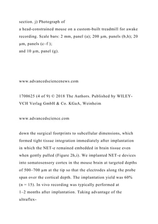
![ibility and the ultrasmall dimensions, we accommodated chronic
optical access concurrently with NET-e implants (Figure 2j)
similarly as we recently demonstrated.[36]
The electrodes on NET-e probes were finished by gold thin
film and had dimensions ranging from 5 × 8 to 12 × 15 µm2
depending on the design. The impedance at 1 kHz ranged
between 1 and 1.8 MΩ, larger than their photolithography-
defined
counterparts,[36] which is consistent with previous results[40]
(Figure 3a). While reducing the dimensions of the neural elec-
trodes is beneficial for recording density and specificity, as
well as tissue compatibility, it leads to the increase of imped-
ance and therefore the decrease of signal-to-noise ratio (SNR).
Conducting polymers such as poly(3,4-ethylenedioxythiophene)
(PEDOT),[41–47] poly(pyrrole),[48] nanomaterials such as
carbon
nanotubes,[49] silicon nano wires,[50] and polymer
nanotubes,[51]
and other functional materials such as IrOx
[1,52] have been used
to decrease electrode impedance and increase charge injec-
tion capacity. We electrochemically deposited PEDOT on the](https://image.slidesharecdn.com/invitedpapersilicon-integratedhigh-densityelectro-221018173726-0381cdf9/85/INVITEDP-A-P-E-RSilicon-Integrated-High-DensityElectro-docx-198-320.jpg)
![NET-e electrodes with an area of 12 × 15 µm2 and observed the
impedance decreased from 0.87 ± 0.33 to 0.046 ± 0.026 MΩ
(Figure 3a, dashed box). The decrease of impedance is expected
to improve the SNR and suppress low-frequency artifact.[51] In
the rest of this work, we only used electrodes without coating
for consistency, whose relatively large impedance combined
with animal motion during awake measurements led to slightly
elevated noise levels, 11.4 ± 1.7 µV (Figure 3b), but all these
electrodes were capable of detecting and isolating single-unit
action potentials. Figure 3c shows the SNR of n = 10 electrode
sites that yielded detectable spikes in three probes implanted
in three mice for 8 weeks. Figure 3d–f shows the representa-
tive recordings, the SNR, and the spike waveforms that were
isolated from the 10 min recording session from three different
electrodes at 2 weeks (Figure 3d) and 5 weeks (Figure 3e,f).
The
recording in Figure 3d had well-isolated single units and was
among the best in signal quality with SNR of 19.0 and a noise
Adv. Sci. 2018, 5, 1700625
Figure 3. In vivo recording performance of NET-e devices. a) In
vivo impedance at 1 kHz measured at 1week after implantation,
n = 20 for each dimen-
sion. Dashed box: impedance of electrodes with PEDOT coating](https://image.slidesharecdn.com/invitedpapersilicon-integratedhigh-densityelectro-221018173726-0381cdf9/85/INVITEDP-A-P-E-RSilicon-Integrated-High-DensityElectro-docx-199-320.jpg)
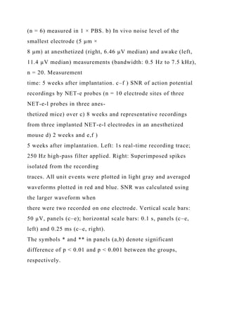
![www.advancedsciencenews.com
1700625 (5 of 9) © 2018 The Authors. Published by WILEY-
VCH Verlag GmbH & Co. KGaA, Weinheim
www.advancedscience.com
level of 7.63 µV. The recording in Figure 3f had discriminable
spike clusters, but was among the worst in signal quality with
an SNR of 8.6 and an average noise level of 6.36 µV. The SNR
is slightly lower but on par with that from its microfabricated
counterparts[36] and other conventional bare electrodes without
polymer coating,[51,53] which is consistent with their reduced
electrode dimension.
Figure 4 shows the representative recording from NET-e-l
electrodes and NET-e-t electrodes, performed 5 and 9 weeks
after implantation, respectively. We used the adjacent
electrodes
in the two designs to estimate their spike detection range,
which depends on its impedance, dimension, and geometry.
The detection range is a crucial parameter to determine the
necessary electrode density for achieving complete detection
of all enclosed neurons within a brain region.[8,23] As shown in](https://image.slidesharecdn.com/invitedpapersilicon-integratedhigh-densityelectro-221018173726-0381cdf9/85/INVITEDP-A-P-E-RSilicon-Integrated-High-DensityElectro-docx-201-320.jpg)
![Figure 4b,c, on NET-e-l electrodes that were separated by 80
µm
along the thread, the same spikes were typically picked up by
adjacent recording sites with strongly attenuated amplitudes,
suggesting that the detection range is comparable to the elec-
trode separation. Consistent with this detection range, the NET-
e-t electrodes recorded temporally correlated spikes from the
four “tetrode-like” electrodes in one group which were densely
packed within an area of 18 µm × 12 µm (Figure 4d,e). The
spatial–temporal correlation of the four electrodes improved
the detection and sorting fidelity of single-unit action potentials
(Figure 4e) analogous to tetrodes.[4] In addition, this scalable
architecture enabled simultaneous detection at multiple brain
depths.
Our previous publication[36] demonstrated that microfabri-
cated NETs afford stable recording and nondegrading tissue–
probe interface in mice through a collection of comprehensive
characterizations. In this work, we did not include systematic
studies on the chronic performance of NET-e probes because
they share similar materials, structures, and the ultraflexibility.
We therefore expect NET-e probes have comparable tissue–
probe interface and recording stability as previously demon-
strated NETs. In the recording period of this study (2 months),
we did not observe chronic deterioration in recording perfor-](https://image.slidesharecdn.com/invitedpapersilicon-integratedhigh-densityelectro-221018173726-0381cdf9/85/INVITEDP-A-P-E-RSilicon-Integrated-High-DensityElectro-docx-202-320.jpg)
![mance (Figure 4f). Similar to the observation of larger
NETs,[36]
in vivo two-photon (2P) imaging 2 months after implantation
showed normal neuronal density (Figure 5a) and morphology
of vasculature (Figure 5b) near the NET-e electrodes. Impor-
tantly and advantageous to the previous larger NET devices, the
much reduced lateral dimensions of NET-e probes allowed for
multiprobe implantation at a previously unattainable high den-
sity. Figure 5c shows the photograph of living brain immedi-
ately after implantation of seven NET-e probes, where the inter-
probe distance was as small as 60 µm, a distance significantly
smaller than the pitch of current state-of-the-art microelec-
trode arrays[31] and would allow electrodes on the two adjacent
probes to have overlapping detection range. We examined post-
mortem tissue–probe interface at 4 months after implantation
(Figure 5d–f). The bright-field images (Figure 5d,e) and the flu-
orescent images from immunohistological staining (Figure 5f)
revealed healthy tissue morphology and normal neuronal den-
sity, suggesting that the long-term presence of NET-e device
Adv. Sci. 2018, 5, 1700625
Figure 4. Representative unit recording from NET-e electrodes.
a) Schematic showing the relative position of electrodes on
NET-e-l (left) and NET-e-t](https://image.slidesharecdn.com/invitedpapersilicon-integratedhigh-densityelectro-221018173726-0381cdf9/85/INVITEDP-A-P-E-RSilicon-Integrated-High-DensityElectro-docx-203-320.jpg)
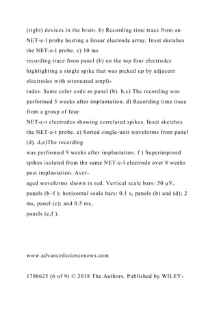
![VCH Verlag GmbH & Co. KGaA, Weinheim
www.advancedscience.com
arrays at high packing density did not result in “dead” zone
near the electrodes. This is also consistent with our previous
study where an unintentionally folded NET probe at a curvature
of about 50 µm in living brain did not elicit astrocytes accumu-
lation at 3.5 months postimplantation.[36]
Different components of the NET-e probes require different
EBL techniques to construct, which were individually optimized
for high yield, throughput, and fabrication resolution. Standard
EBL using poly(methyl methacrylate) (PMMA) as the positive
resist followed by metallization and lift-off was performed to
define the interconnects and the electrodes. The highest resolu-
tion was required for interconnect traces, which is determined
by the EBL sample stage stitching error, because the length of
the thread (about 1 mm) was much larger than the size of the
writing field in the EBL tool used in this work (80 µm). Non-
standard EBL was performed to construct the insulation layers,
for which we tested both PMMA[54] and SU-8[55] as negative
EBL resists. These two resists were chosen for their good insu-
lation, excellent tensile strength after hard baking, and tun-](https://image.slidesharecdn.com/invitedpapersilicon-integratedhigh-densityelectro-221018173726-0381cdf9/85/INVITEDP-A-P-E-RSilicon-Integrated-High-DensityElectro-docx-205-320.jpg)
![able thickness depending on the exposure doses.[54,55] Because
PMMA requires a high dose of about 40 000 µC cm−2 to cross-
link[54] that leads to prohibitively long EBL exposure times
even
at high currents, we chose to use SU-8 for higher fabrication
throughput.
Our fabrication yield was about 70% with little variation
among different design patterns that required fabrication reso-
lution ranging between 200 and 400 nm. We have thoroughly
examined our fabrication process and identified that the yield
loss is mainly due to fabrication defects. All fabrication proce-
dures, including four EBL steps, seven photolithography steps,
and five metal deposition steps, were performed manually,
which make it difficult to completely avoid microparticles and
scratches especially on the long, narrow interconnect traces.
The
EBL exposure time was relatively short. For example, an entire
4″
wafer that contains 8 NET-e devices and a total of 256
electrodes
typically requires exposure times of ≈5 min for the insulating
layers composed of SU-8, 2 h for the interconnects, and 15 min
for the electrode layers. However, the fabrication throughput
was mostly limited by the two-step iterative alignment pro-](https://image.slidesharecdn.com/invitedpapersilicon-integratedhigh-densityelectro-221018173726-0381cdf9/85/INVITEDP-A-P-E-RSilicon-Integrated-High-DensityElectro-docx-206-320.jpg)
![cess during EBL that was necessary for sub-100 nm registra-
tion accuracy across the entire wafer. Despite the relatively low
throughput compared with photolithography, the application of
EBL greatly improved the fabrication resolution and reduced the
probe’s overall dimensions, and further offers great flexibility
in
patterning nanoscale structures by design. We are confident that
the fabrication yield, throughput, and resolution can be further
improved using more advanced EBL equipment.
Ultraflexibility requires additional efforts in careful han-
dling and implantation. However, ultraflexibility is necessary
to achieve stable chronical recording and nondegrading tissue–
probe interface.[36] Significantly different from our previous
work that focused on the chronically stable recording and non-
degrading tissue–probe interface, this work focused on pushing
the dimensional limit of ultraflexible neural electrodes on a
similar device architecture. Using nanofabrication and refined
implantation techniques, we further reduced both the device
cross-sectional area and the surgical footprints per recording
site by an order of magnitude. Importantly and advantageous to
the previous larger NET devices, the much reduced dimensions
of NET-e probes allowed for multiprobe implantation at a pre-
viously unattainable high density (e.g., 60 µm interprobe dis-
tance) without eliciting observable neuronal death over chronic](https://image.slidesharecdn.com/invitedpapersilicon-integratedhigh-densityelectro-221018173726-0381cdf9/85/INVITEDP-A-P-E-RSilicon-Integrated-High-DensityElectro-docx-207-320.jpg)
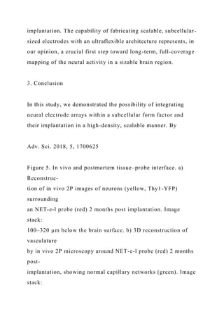

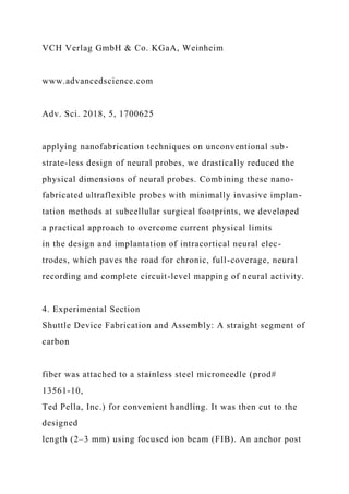
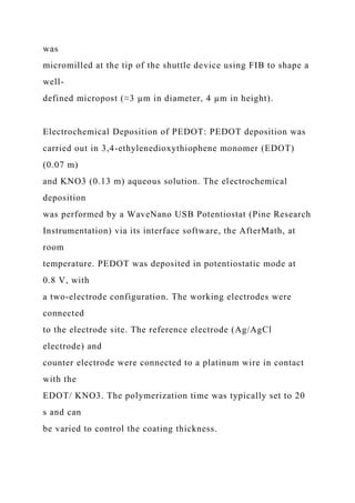
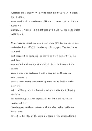
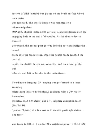
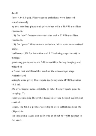
![Awake Electrophysiological Recording: Mice were allowed a 1–
2 week
recovery period after surgery. For recording, mice were head
constrained
on a custom-made air-supported spherical treadmill to allow
walking and running, similar to the setup previously used for
optical
imaging.[44] The treadmill was made of an 8″ diameter
Styrofoam ball
(Floracraft) levitated by a thin cushion of air between the ball
and a
casting containing air jets. Voltage signals from the NEC
devices were
amplified and digitized using a 32-channel RHD 2132
evaluation system
(Intan Technologies) with a bare Ag wire inserted into the
contralateral
hemisphere of the brain as the grounding reference. The
sampling
rate was 20 kHz, and a 300 Hz high-pass and a 60 Hz notch
filter were
applied for single-unit recording. Mice and the amplifier were
placed
in a noise-attenuated, electrically shielded chamber. Impedance](https://image.slidesharecdn.com/invitedpapersilicon-integratedhigh-densityelectro-221018173726-0381cdf9/85/INVITEDP-A-P-E-RSilicon-Integrated-High-DensityElectro-docx-216-320.jpg)
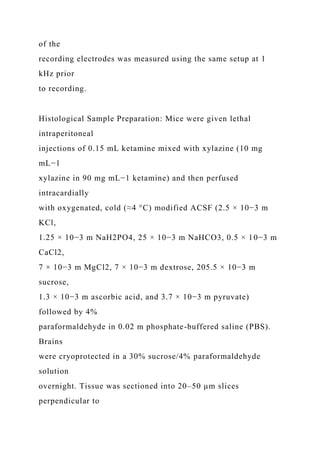

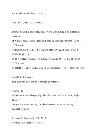
![Published online: March 10, 2018
[1] N. A. Kotov, J. O. Winter, I. P. Clements, E. Jan, B. P.
Timko,
S. Campidelli, S. Pathak, A. Mazzatenta, C. M. Lieber, M.
Prato,
R. V. Bellamkonda, G. A. Silva, N. W. S. Kam, F. Patolsky, L.
Ballerini,
Adv. Mater. 2009, 21, 3970.
[2] P. Fattahi, G. Yang, G. Kim, M. R. Abidian, Adv. Mater.
2014, 26,
1846.
[3] M. A. Nicolelis, A. A. Ghazanfar, B. M. Faggin, S. Votaw,
L. M. Oliveira, Neuron 1997, 18, 529.
[4] C. M. Gray, P. E. Maldonado, M. Wilson, B. McNaughton,
J. Neu-
rosci. Methods 1995, 63, 43.
[5] K. D. Wise, J. B. Angell, A. Starr, IEEE Trans. Biomed.
Eng. 1970, 17,
238.](https://image.slidesharecdn.com/invitedpapersilicon-integratedhigh-densityelectro-221018173726-0381cdf9/85/INVITEDP-A-P-E-RSilicon-Integrated-High-DensityElectro-docx-221-320.jpg)
![[6] P. K. Campbell, K. E. Jones, R. J. Huber, K. W. Horch, R.
A. Normann,
IEEE Trans. Biomed. Eng. 1991, 38, 758.
[7] Q. Bai, K. D. Wise, IEEE Trans. Biomed. Eng. 2001, 48,
911.
[8] A. P. Alivisatos, M. Chun, G. M. Church, K. Deisseroth,
J. P. Donoghue, R. J. Greenspan, P. L. McEuen, M. L. Roukes,
T. J. Sejnowski, P. S. Weiss, R. Yuste, Science 2013, 339,
1284.
[9] G. Buzsaki, Nat. Neurosci. 2004, 7, 446.
[10] M. Carandini, Nat. Neurosci. 2012, 15, 507.
[11] M. E. Spira, A. Hai, Nat. Nanotechnol. 2013, 8, 83.
[12] M. K. Lyons, Mayo Clin. Proc. 2011, 86, 662.
[13] M. S. Sharifi, Basic Clin. Neurosci. 2013, 4, 266.
[14] P. Krack, A. Batir, N. Van Blercom, S. Chabardes, V.
Fraix,
C. Ardouin, A. Koudsie, P. D. Limousin, A. Benazzouz, J. F.
LeBas,
A. L. Benabid, P. Pollak, N. Engl. J. Med. 2003, 349, 1925.](https://image.slidesharecdn.com/invitedpapersilicon-integratedhigh-densityelectro-221018173726-0381cdf9/85/INVITEDP-A-P-E-RSilicon-Integrated-High-DensityElectro-docx-222-320.jpg)
![[15] P. Boon, R. Raedt, V. de Herdt, T. Wyckhuys, K. Vonck,
Neurothera-
peutics 2009, 6, 218.
[16] L. R. Hochberg, M. D. Serruya, G. M. Friehs, J. A.
Mukand, M. Saleh,
A. H. Caplan, A. Branner, D. Chen, R. D. Penn, J. P. Donoghue,
Nature 2006, 442, 164.
[17] L. R. Hochberg, D. Bacher, B. Jarosiewicz, N. Y. Masse, J.
D. Simeral,
J. Vogel, S. Haddadin, J. Liu, S. S. Cash, P. van der Smagt,
J. P. Donoghue, Nature 2012, 485, 372.
[18] P. J. Rousche, R. A. Normann, J. Neurosci. Methods 1998,
82, 1.
[19] S. L. BeMent, K. D. Wise, D. J. Anderson, K. Najafi, K. L.
Drake,
IEEE Trans. Biomed. Eng. 1986, 33, 230.
[20] D. R. Kipke, R. J. Vetter, J. C. Williams, J. F. Hetke, IEEE
Trans.
Neural Syst. Rehabil. Eng. 2003, 11, 151.
[21] V. S. Polikov, P. A. Tresco, W. M. Reichert, J. Neurosci.](https://image.slidesharecdn.com/invitedpapersilicon-integratedhigh-densityelectro-221018173726-0381cdf9/85/INVITEDP-A-P-E-RSilicon-Integrated-High-DensityElectro-docx-223-320.jpg)
![Methods 2005,
148, 1.
[22] J. P. Seymour, D. R. Kipke, Biomaterials 2007, 28, 3594.
[23] A. H. Marblestone, B. M. Zamft, Y. G. Maguire, M. G.
Shapiro,
T. R. Cybulski, J. I. Glaser, D. Amodei, P. B. Stranges, R.
Kalhor,
D. A. Dalrymple, D. Seo, E. Alon, M. M. Maharbiz, J. M.
Carmena,
J. M. Rabaey, E. S. Boyden, G. M. Church, K. P. Kording, Front
Comput. Neurosci. 2013, 7, 137.
[24] A. C. Patil, N. V. Thakor, Med. Biol. Eng. Comput. 2016,
54, 23.
[25] J. Viventi, D. H. Kim, L. Vigeland, E. S. Frechette, J. A.
Blanco,
Y. S. Kim, A. E. Avrin, V. R. Tiruvadi, S. W. Hwang, A. C.
Vanleer,
D. F. Wulsin, K. Davis, C. E. Gelber, L. Palmer, J. Van der
Spiegel,
J. Wu, J. L. Xiao, Y. G. Huang, D. Contreras, J. A. Rogers, B.
Litt,](https://image.slidesharecdn.com/invitedpapersilicon-integratedhigh-densityelectro-221018173726-0381cdf9/85/INVITEDP-A-P-E-RSilicon-Integrated-High-DensityElectro-docx-224-320.jpg)
![Nat. Neurosci. 2011, 14, 1599.
[26] D. C. Rodger, A. J. Fong, L. Wen, H. Ameri, A. K. Ahuja,
C. Gutierrez,
I. Lavrov, Z. Hui, P. R. Menon, E. Meng, J. W. Burdick, R. R.
Roy,
V. R. Edgerton, J. D. Weiland, M. S. Humayun, Y. C. Tai, Sens.
Actua-
tors, B 2008, 132, 449.
[27] T. D. Y. Kozai, N. B. Langhals, P. R. Patel, X. P. Deng, H.
N. Zhang,
K. L. Smith, J. Lahann, N. A. Kotov, D. R. Kipke, Nat. Mater.
2012,
11, 1065.
[28] L. W. Tien, F. Wu, M. D. Tang-Schomer, E. Yoon, F. G.
Omenetto,
D. L. Kaplan, Adv. Funct. Mater. 2013, 23, 3185.
[29] N. F. Nolta, M. B. Christensen, P. D. Crane, J. L. Skousen,
P. A. Tresco, Biomaterials 2015, 53, 753.
[30] J. Scholvin, J. P. Kinney, J. G. Bernstein, C. Moore-
Kochlacs,](https://image.slidesharecdn.com/invitedpapersilicon-integratedhigh-densityelectro-221018173726-0381cdf9/85/INVITEDP-A-P-E-RSilicon-Integrated-High-DensityElectro-docx-225-320.jpg)
![N. Kopell, C. G. Fonstad, E. S. Boyden, IEEE Trans. Biomed.
Eng.
2016, 63, 120.
[31] G. Rios, E. V. Lubenov, D. Chi, M. L. Roukes, A. G.
Siapas, Nano
Lett. 2016, 16, 6857.
[32] J. Du, T. J. Blanche, R. R. Harrison, H. A. Lester, S. C.
Masmanidis,
PLoS One 2011, 6, e26204.
[33] C. M. Lopez, S. Mitra, J. Putzeys, B. Raducanu, M. Ballini,
A. Andrei, S. Severi, M. Welkenhuysen, C. Van Hoof, S. Musa,
R. F. Yazicioglu, in 2016 IEEE Int. Solid-State Circuits Conf.
(ISSCC),
(Ed.: L. C. Fujino), Vol. 59, IEEE, San Francisco, CA, USA
2016,
p. 392.
[34] C. Xie, J. Liu, T. M. Fu, X. Dai, W. Zhou, C. M. Lieber,
Nat. Mater.
2015, 14, 1286.
[35] T. M. Fu, G. Hong, T. Zhou, T. G. Schuhmann, R. D.](https://image.slidesharecdn.com/invitedpapersilicon-integratedhigh-densityelectro-221018173726-0381cdf9/85/INVITEDP-A-P-E-RSilicon-Integrated-High-DensityElectro-docx-226-320.jpg)
![Viveros,
C. M. Lieber, Nat. Methods 2016, 13, 875.
[36] L. Luan, X. Wei, Z. Zhao, J. J. Siegel, O. Potnis, C. A.
Tuppen, S. Lin,
S. Kazmi, R. A. Fowler, S. Holloway, A. K. Dunn, R. A.
Chitwood,
C. Xie, Sci. Adv. 2017, 3, e1601966.
[37] Z. Zhao, L. Luan, X. Wei, H. Zhu, X. Li, S. Lin, J. J.
Siegel,
R. A. Chitwood, C. Xie, Nano Lett. 2017, 17, 4588.
[38] J. C. Potosky, A. J. Higgins, S. T. Hoelke, R. G. Imerson,
F. F. Kinoshita, R. L. Maddox, J. P. Reekstin, J. Vac. Sci.
Technol.
1981, 19, 924.
[39] S. H. Felix, K. G. Shah, V. M. Tolosa, H. J. Sheth, A. C.
Tooker,
T. L. Delima, S. P. Jadhav, L. M. Frank, S. S. Pannu, J.
Visualized Exp.
2013, 79, e50609.
[40] A. K. Ahuja, M. R. Behrend, J. J. Whalen, M. S. Humayun,](https://image.slidesharecdn.com/invitedpapersilicon-integratedhigh-densityelectro-221018173726-0381cdf9/85/INVITEDP-A-P-E-RSilicon-Integrated-High-DensityElectro-docx-227-320.jpg)
![J. D. Weiland, IEEE Trans. Biomed. Eng. 2008, 55, 1457.
[41] D. Khodagholy, J. N. Gelinas, T. Thesen, W. Doyle, O.
Devinsky,
G. G. Malliaras, G. Buzsaki, Nat. Neurosci. 2015, 18, 310.
[42] K. A. Ludwig, N. B. Langhals, M. D. Joseph, S. M.
Richardson-
Burns, J. L. Hendricks, D. R. Kipke, J. Neural. Eng. 2011, 8,
014001.
[43] M. Sessolo, D. Khodagholy, J. Rivnay, F. Maddalena, M.
Gleyzes,
E. Steidl, B. Buisson, G. G. Malliaras, Adv. Mater. 2013, 25,
2135.
[44] M. R. Abidian, J. M. Corey, D. R. Kipke, D. C. Martin,
Small 2010,
6, 421.
[45] R. Green, M. R. Abidian, Adv. Mater. 2015, 27, 7620.
[46] G. Malliaras, M. R. Abidian, Adv. Mater. 2015, 27, 7492.
[47] S. Park, G. Yang, N. Madduri, M. R. Abidian, S. Majd,
Adv. Mater.](https://image.slidesharecdn.com/invitedpapersilicon-integratedhigh-densityelectro-221018173726-0381cdf9/85/INVITEDP-A-P-E-RSilicon-Integrated-High-DensityElectro-docx-228-320.jpg)
![2014, 26, 2782.
[48] M. Antensteiner, M. Khorrami, F. Fallahianbijan, A.
Borhan,
M. R. Abidian, Adv. Mater. 2017, 29, 1702576.
www.advancedsciencenews.com
1700625 (9 of 9) © 2018 The Authors. Published by WILEY-
VCH Verlag GmbH & Co. KGaA, Weinheim
www.advancedscience.com
Adv. Sci. 2018, 5, 1700625
[49] V. Lovat, D. Pantarotto, L. Lagostena, B. Cacciari, M.
Grandolfo,
M. Righi, G. Spalluto, M. Prato, L. Ballerini, Nano Lett. 2005,
5,
1107.
[50] F. Patolsky, B. P. Timko, G. H. Yu, Y. Fang, A. B.
Greytak,](https://image.slidesharecdn.com/invitedpapersilicon-integratedhigh-densityelectro-221018173726-0381cdf9/85/INVITEDP-A-P-E-RSilicon-Integrated-High-DensityElectro-docx-229-320.jpg)
![G. F. Zheng, C. M. Lieber, Science 2006, 313, 1100.
[51] M. R. Abidian, K. A. Ludwig, T. C. Marzullo, D. C.
Martin,
D. R. Kipke, Adv. Mater. 2009, 21, 3764.
[52] Z. C. Lin, C. Xie, Y. Osakada, Y. Cui, B. Cui, Nat.
Commun. 2014, 5,
3206.
[53] R. J. Vetter, J. C. Williams, J. F. Hetke, E. A. Nunamaker,
D. R. Kipke,
IEEE Trans. Biomed. Eng. 2004, 51, 896.
[54] A. C. F. Hoole, M. E. Welland, A. N. Broers, Semicond.
Sci. Technol.
1997, 12, 1166.
[55] A. K. Nallani, S. W. Park, J. B. Lee, Proc. SPIE 2003,
5116, 414.
COMMUNICATION](https://image.slidesharecdn.com/invitedpapersilicon-integratedhigh-densityelectro-221018173726-0381cdf9/85/INVITEDP-A-P-E-RSilicon-Integrated-High-DensityElectro-docx-230-320.jpg)
![www.advmat.de
1706520 (1 of 7) © 2018 The Authors. Published by WILEY-
VCH Verlag GmbH & Co. KGaA, Weinheim
High-Density Stretchable Electrode Grids for Chronic
Neural Recording
Klas Tybrandt,* Dion Khodagholy,* Bernd Dielacher, Flurin
Stauffer, Aline F. Renz,
György Buzsáki, and János Vörös
Dr. K. Tybrandt, Dr. B. Dielacher, Dr. F. Stauffer, A. F. Renz,
Prof. J. Vörös
Institute for Biomedical Engineering
ETH Zurich
8092 Zurich, Switzerland
E-mail: [email protected]
Dr. K. Tybrandt
Laboratory of Organic Electronics
Department of Science and Technology
Linköping University
601 74 Norrköping, Sweden
Dr. D. Khodagholy
Department of Electrical Engineering
Columbia University](https://image.slidesharecdn.com/invitedpapersilicon-integratedhigh-densityelectro-221018173726-0381cdf9/85/INVITEDP-A-P-E-RSilicon-Integrated-High-DensityElectro-docx-231-320.jpg)
![New York, NY 10027, USA
E-mail: [email protected]
Dr. D. Khodagholy, Prof. G. Buzsáki
NYU Neuroscience Institute
School of Medicine
New York University
New York, NY 10016, USA
DOI: 10.1002/adma.201706520
Electrical stimulation has successfully
been applied to treat neurological disor-
ders like Parkinson’s disease, epilepsy,
hearing loss, and chronic pain. One
reason for this success is that electrical
stimulation can compensate for scar
tissue encapsulation of electrodes by
increasing the stimulation current and
thereby continuing to reach the stimula-
tion threshold.[1] However, current and
emerging therapies would benefit from
the use of closed feedback systems, in
which recorded signals are used to con-
trol the stimulation for optimal effect.[2,3]
This approach requires the establishment](https://image.slidesharecdn.com/invitedpapersilicon-integratedhigh-densityelectro-221018173726-0381cdf9/85/INVITEDP-A-P-E-RSilicon-Integrated-High-DensityElectro-docx-232-320.jpg)
![of a well-integrated, long-term stable, elec-
tronic–neural interface to pick up weak
neural signals. One major factor which
restricts the long-term stability of neural
interfaces is the huge mechanical mis-
match between electronics and neural
tissue.[4] Even plastic substrates exhibit
elastic moduli in the GPa range, while neural tissue is vis-
coelastic with elastic moduli in the kPa range.[5] As neural
tissue constantly endures bodily motions and deformations,
stiff implants will cause mechanical wear at the interface,
leading to tissue responses with deteriorating performance
of the implant.[4,6–8] To avoid this effect, neural implants need
to be engineered out of materials that match the mechanical
properties of the interfaced tissue as closely as possible.[9–11]
Flexible electrode grids[12,13] and penetrating probes[14,15]
have
been developed to improve the electrode–tissue interface. In
recent years, further steps in this direction have been taken
by the development of soft and stretchable electrically con-
ductive composites, typically comprising a conductive filler
embedded in an elastomer matrix.[16–21] Biomedical implants
have a strict set of material requirements, including long-term
stability, nontoxicity, and biocompatibility. This disqualifies](https://image.slidesharecdn.com/invitedpapersilicon-integratedhigh-densityelectro-221018173726-0381cdf9/85/INVITEDP-A-P-E-RSilicon-Integrated-High-DensityElectro-docx-233-320.jpg)
![most reported composites, as silver is unstable and toxic,[1,10]
while carbon nanotube based composites require detergents/
ionic liquids that may leak out into the tissue.[18] Microcracked
gold is to date the premier example of an implantable stretch-
able conductor,[22,23] and it has been used to fabricate soft and
stretchable electrode arrays for stimulation and recording.[11]
Although very useful, microcracked gold has high sheet resist-
ance and reported fabrication protocols have not allowed for
the far-reaching miniaturization necessary for high-resolution
neural recording. To tackle these limitations, here we report
on the development of a novel inert high-performance
Electrical interfacing with neural tissue is key to advancing
diagnosis and
therapies for neurological disorders, as well as providing
detailed information
about neural signals. A challenge for creating long-term stable
interfaces
between electronics and neural tissue is the huge mechanical
mismatch
between the systems. So far, materials and fabrication processes
have restricted
the development of soft electrode grids able to combine high
performance,
long-term stability, and high electrode density, aspects all](https://image.slidesharecdn.com/invitedpapersilicon-integratedhigh-densityelectro-221018173726-0381cdf9/85/INVITEDP-A-P-E-RSilicon-Integrated-High-DensityElectro-docx-234-320.jpg)
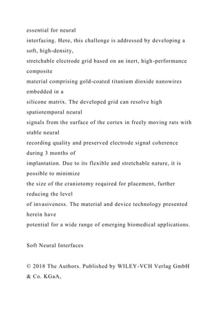

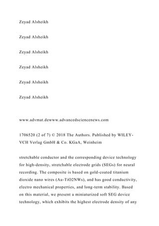
![When 1/10 of the gold salt had been added, the TiO2NWs
were partially covered by a thin layer of gold (Figure 1c).
Once all gold salt had been reduced, the TiO2NWs were fully
covered by a rough layer of gold (Figure 1d,e). A week after
adding the hydrochloric acid, the roughness of the gold coating
had decreased significantly (Figure 1e). For electrical charac-
terization, samples of 0.5 mm width and 20 mm length were
prepared by masked vacuum filtration.[24] First, the nanowire
dispersion was filtered through, followed by a rinsing step
of phosphate-buffered saline (PBS) filtration and drying on a
hotplate. Samples prepared from fresh dispersions showed
decreasing sheet resistance over time (Figure 1f). A similar
trend emerged for samples prepared from stored dispersions
(Figure 1f). Stretchable samples were fabricated by transferring
the Au-TiO2NW patterns from the filter membranes to semi-
cured poly(dimethylsiloxane) (PDMS) substrates, followed by
spin coating of a top PDMS layer to encapsulate the Au-
TiO2NW
tracks. The initial sheet resistance of the ≈3 µm thick tracks
was 0.63 ± 0.03 Ω □−1, which translates into a conductivity of
≈16000 S cm−1. When stretched, the sheet resistance increased
to ≈3 Ω □−1 for 50% strain and ≈7 Ω □−1 for 100% strain.
Some
samples started to lose electrical contact above 100% strain, and](https://image.slidesharecdn.com/invitedpapersilicon-integratedhigh-densityelectro-221018173726-0381cdf9/85/INVITEDP-A-P-E-RSilicon-Integrated-High-DensityElectro-docx-239-320.jpg)
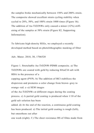

![Zeyad Alsheikh
Zeyad Alsheikh
Zeyad Alsheikh
Zeyad Alsheikh
Zeyad Alsheikh
Zeyad Alsheikh
www.advmat.dewww.advancedsciencenews.com
1706520 (3 of 7) © 2018 The Authors. Published by WILEY-
VCH Verlag GmbH & Co. KGaA, Weinheim
membranes.[25] The method can produce arbitrary nanowire
patterns down to 20 µm sized features and yields high
performance, narrow, stretchable conductor lines. The
Au-TiO2NW dispersion was filtered through the masked mem-
brane, cleaned by filtering of PBS buffer, dried, and then trans-
ferred to a semi-cured PDMS substrate (≈75 µm thick). The
membrane was wetted from the backside and peeled off, leaving](https://image.slidesharecdn.com/invitedpapersilicon-integratedhigh-densityelectro-221018173726-0381cdf9/85/INVITEDP-A-P-E-RSilicon-Integrated-High-DensityElectro-docx-242-320.jpg)
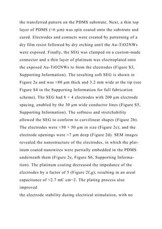
![degradation in performance after 106 bipolar pulses (1 V,
200 µs) of the physiologically relevant current range of 100 µA
(Figure S7, Supporting Information). When the electrodes were
stretched to 30% strain (Figure 2h), the impedance decreased
slightly in accordance with the increase in electrode area
(Figure 2i). A batch of 16 SEGs was fabricated for this study,
of which 7 devices were fully functional. The defective SEGs
had a few breaks on the narrow conductor lines and were there-
fore discarded.
In vivo evaluation and characterization of the SEGs were
carried out in rats by implanting probes on the somatosensory
cortex (Figure 3a) to record somatosensory evoked potentials
(SSEPs).[26] The recordings were performed both acutely in the
intraoperative setting, as well as chronically in freely moving
rats
(Figure 3c), to further characterize the spatiotemporal
resolution
of neural signals captured by the soft and stretchable probes.
Owing to the softness and stretchability of the SEG, it could be
folded on itself and inserted through an ≈30% narrower crani-
otomy window than its original size. Once inserted, the grid
self-
expanded onto the pial cortical surface (Figure 3b). For chronic
in vivo recording, the grid was covered with a piece of bioab-](https://image.slidesharecdn.com/invitedpapersilicon-integratedhigh-densityelectro-221018173726-0381cdf9/85/INVITEDP-A-P-E-RSilicon-Integrated-High-DensityElectro-docx-244-320.jpg)
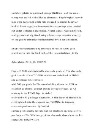
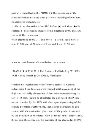
![for various frequency bands (1 to 90 Hz) in the chronically
implanted SEG (Figure 4d). As predicted by theoretical models
of the spatial scale of the local field potential (LFP),[27,28]
coher-
ence was high at low frequencies and decreased for higher
frequencies, highlighting the physiological nature of these
oscillations. Moreover, these analyses suggested that LFP pat-
terns can be differentiated at sub-millimeter distances and that
high spatiotemporal resolution sampling of neural activity can
provide information about physiological cortical processes. The
recording quality was stable over time, as the average power
of the recorded signals was similar after 1, 2, and 3 months of
implantation (Figure 4e). After 3 months, 28 electrodes showed
excellent signal quality, 3 had weaker signals, and only one
elec-
trode was dead (Figure 4f, Figure S8 in the Supporting Infor-
mation). As the failing electrodes were not adjacent to each
other, but connected next to each other on one side of the con-
nector (Figure S4, Supporting Information), it is likely that the
failure is related to the grid-connector contact rather than the
stretchable conductor or the electrode–tissue interface.
The coating of the TiO2NWs starts by the formation of a thin,
partially covering gold layer. As the pH of the dispersion ranges
from 6 to 7 during the synthesis, the titanium dioxide is neu-](https://image.slidesharecdn.com/invitedpapersilicon-integratedhigh-densityelectro-221018173726-0381cdf9/85/INVITEDP-A-P-E-RSilicon-Integrated-High-DensityElectro-docx-248-320.jpg)
![tral[29] while the gold (nanoparticles) are negatively
charged.[30]
As PVP further reduces any surface charge, the adsorption of
the initial gold layer is thus probably not driven by electrostatic
forces, but rather by van der Waal’s attraction. This hypothesis
suggests that other template materials, like carbon nanotubes
or fibers, could be used in a similar fashion, although little
gain in performance would be expected due to the superior
conductivity of gold. The coating process is effective, as no free
gold (nano)particles can be seen in the SEM images or in the
filtrate. This is probably due to the chosen reducing agent’s
Adv. Mater. 2018, 30, 1706520
Figure 3. Implantation and in vivo neural recording of soft
SEGs. a) Intraoperative microphotograph of soft SEG showing
the probe in a craniotomy
lying on the surface of the brain. Note the hydrophobic nature
of the device demonstrated by a drop of water on the ribbon
area. b) Zoomed-in
microscopy image showing the ability of the probe to be
inserted in smaller craniotomy than the probe geometry. c)
Freely moving rat with chronically
implanted SEG. d) Intraoperative recording of SSEPs using the
soft SEG. Top: raw LFP time traces showing SSEPs generated](https://image.slidesharecdn.com/invitedpapersilicon-integratedhigh-densityelectro-221018173726-0381cdf9/85/INVITEDP-A-P-E-RSilicon-Integrated-High-DensityElectro-docx-249-320.jpg)
![by hind limb electrical
stimulation. Right: heat map demonstrating the anatomical
localization of SSEPs to the somatosensory cortex. Left: electric
impedance of the SEGs at
1 kHz, showing a uniform impedance range across devices.
Scale bars: a,b) 1 mm, c) 10 mm, d) 100 ms, 500 µV.
www.advmat.dewww.advancedsciencenews.com
1706520 (5 of 7) © 2018 The Authors. Published by WILEY-
VCH Verlag GmbH & Co. KGaA, Weinheim
surface-catalyzed reduction of Au3+, which prevents continuous
seeding of new gold nanoparticles.[31] The addition of HCl
to the dispersion induces a gradual color change, which is
caused by smoothening of the initially rough gold surface. The
smoothening improves the electrical conductivity, giving the
Au-TiO2NW-PDMS composite a conductivity of ≈16000 S
cm−1,
which compares well with previously reported stretchable com-
posites.[16,17,20,32] Even better, the electromechanical
character-
istics remain stable after one thousand strain cycles of 100%](https://image.slidesharecdn.com/invitedpapersilicon-integratedhigh-densityelectro-221018173726-0381cdf9/85/INVITEDP-A-P-E-RSilicon-Integrated-High-DensityElectro-docx-250-320.jpg)
![strain, which is important for a material considered for long-
term use. A possible explanation for this advantageous behavior
is the small size of the cracks in the composite under strain
(Figure S9, Supporting Information) in comparison to silver
nanowire-based composites.[24] This observation might in turn
be related to the relatively low degree of stiffening caused by
the Au-TiO2NWs.
The fact that Au-TiO2NWs are long-term stable and can be
dispersed in water without ultrasonication makes the mate-
rial convenient to use. Further, the developed filtration method
exhibits certain advantages for biomedical applications: (i) the
material consumption is low which allows for the use of expen-
sive noble metals; (ii) the nanowires can easily be cleaned in
the process, thereby removing potentially harmful chemicals;
(iii) the method yields high-quality micro-patterns that enable
high electrode density; (iv) PDMS or other medical grade
silicones can be used in the process; (v) the patterning process
does not expose the sensitive PDMS substrate to any aggres-
sive organic solvents or potentially harmful substances. The
impedance of the microelectrodes is around 10 kΩ at 1 kHz in
PBS, which is low enough for high-quality recordings. When
fitting an equivalent circuit to the impedance data (Figure S10,
Supporting Information), a constant phase element is needed.](https://image.slidesharecdn.com/invitedpapersilicon-integratedhigh-densityelectro-221018173726-0381cdf9/85/INVITEDP-A-P-E-RSilicon-Integrated-High-DensityElectro-docx-251-320.jpg)
![This indicates that the electrodes are porous, which is in line
with the high areal capacitance (2.7 mC cm−2) and the SEM
images. Our SEG outperforms previously reported devices in
terms of electromechanical properties, electrode density, and
electrode performance (Table 1), all key features for high-
quality
neural recording. Also, our SEG has demonstrated stable
neural recordings for the longest period of any implanted SEG.
Although nanomaterials are great for electrode performance,
one need to consider the risk of nanotoxicity, often mediated
through the creation of reactive oxygen species (ROS).[33]
TiO2
nanoparticles have been found to cause relatively low levels of
ROS induced stress in cells.[34,35] However, this should not be
an issue in this work as the electrodes and Au-TiO2NWs can
be fabricated without any visible exposure of TiO2 (Figure S6,
Supporting Information). Overall, these features make the
developed technology a premier candidate for a wide range of
biomedical applications.
The soft and stretchable nature of the SEG allowed us to per-
form craniotomies that were smaller than the probe’s geometry,
reducing the risk of surgical complications and cerebral
swelling.
Moreover, the hydrophobic surface of the probe provided an](https://image.slidesharecdn.com/invitedpapersilicon-integratedhigh-densityelectro-221018173726-0381cdf9/85/INVITEDP-A-P-E-RSilicon-Integrated-High-DensityElectro-docx-252-320.jpg)

![0.5 mL) was added 5 min after completion. The dispersion was
put through a 20 µm stainless steel sieve to remove eventual
large
aggregates. The dispersion was stored for at least 1 d before
use. SEM
images were taken with a Zeiss Leo 1530.
Electromechanical Characterization: Au-TiO2NW tracks (20
mm
length, 0.5 mm width) with contact pads were patterned by wax
assisted
vacuum filtration[24] (4 mL Au-TiO2NW solution, 200 mm
2 open filter
area) and transferred to a semi-cured PDMS sample (Sylgard
184,
Dow Corning, 1:10, 1 krpm spin speed, 30 s, 6 min 70 °C
curing). A
diluted PDMS solution (PDMS:heptane 1:20) was spin coated (6
krpm
60 s) to reinforce the contact pads and cured (80 °C, 20 min). A
25 µm
poly(ethylene naphthalate) foil was used to mask the contact
pads and
a layer of PDMS was spin-coated on top (2 krpm 30 s). The foil](https://image.slidesharecdn.com/invitedpapersilicon-integratedhigh-densityelectro-221018173726-0381cdf9/85/INVITEDP-A-P-E-RSilicon-Integrated-High-DensityElectro-docx-256-320.jpg)
![was
removed and the samples were cured (80 °C, 16 h). The samples
were
clamped in a tensile testing machine (DO-FB0.5TS,
Zwick/Roell) with
copper tape as contacts. A digital multimeter (Agilent 34401A)
was used
to measure the resistance at 4 Hz. The strain rate was 0.5 mm
s−1 for
the maximum strain tests and 2 mm s−1 for the cycling tests.
SEG Fabrication and Characterization: Hydrophilic PVDF
membranes
(0.22 µm pore size, Millipore) were patterned with ma-N 490
photoresist (micro resist technology GmbH) according to
previously
published protocol.[25] Au-TiO2NW dispersion (1.8 mL, 92 mm
2 open
filter area) followed by PBS buffer (10 mL) was vacuum filtered
through
the patterned membrane. PDMS was spin-coated (Sylgard 184, 1
krpm
spin speed, 30 s) onto a silanized 2 inch glass wafer and semi-
cured](https://image.slidesharecdn.com/invitedpapersilicon-integratedhigh-densityelectro-221018173726-0381cdf9/85/INVITEDP-A-P-E-RSilicon-Integrated-High-DensityElectro-docx-257-320.jpg)


![The authors acknowledge M. Lanz and S. Wheeler for their
valuable
technical support, and the support of the ETH ScopeM facility
for
performing scanning electron microscopy experiments. The
research
was financed by the Swedish Research Council (637-2013-
7301), the
Swedish Government Strategic Research Area in Materials
Science on
Functional Materials at Linköping University (Faculty Grant
SFO Mat
LiU No 2009 00971), the Swiss Nanotera SpineRepair project,
and ETH
Adv. Mater. 2018, 30, 1706520
Table 1. Comparison between the SEG in this work and
previously reported SEGs.
Conductor RS
[Ω]
Max strain
[%]](https://image.slidesharecdn.com/invitedpapersilicon-integratedhigh-densityelectro-221018173726-0381cdf9/85/INVITEDP-A-P-E-RSilicon-Integrated-High-DensityElectro-docx-261-320.jpg)
![Electrode
material
Electrode
count
Electrode densityc)
[mm−2]
Electrode size
[103 µm2]
|Z|d) at
1 kHz [kΩ]
|Z|·Ae) at
1 kHz [kΩ cm2]
Implantation
period [weeks]
Ref.
Au-TiO2-NWs 0.6 100 Pt plated NWs 32 38 3 10 0.3 13 This](https://image.slidesharecdn.com/invitedpapersilicon-integratedhigh-densityelectro-221018173726-0381cdf9/85/INVITEDP-A-P-E-RSilicon-Integrated-High-DensityElectro-docx-262-320.jpg)
![work
PPy/PCTC 6 23 PPy/PCTC 4 0.2 800 10 80 Acute [36]
PPy/PTSA 8 9b) PPy/PTSA 4 0.9 200 30 60 Acute [37]
Au film 35 nm 9a) >45 Pt-PDMS 9 3 70 3 2 6 [11]
Au film 50–150 nm - ≈10 Au 11 3 3 200 6 in vitro [38]
Au film 38 nm – ≈10 Pt 28 11 10 100 10 in vitro [39]
a)RS not given, adopted from ref. [22];
b)In prestrained device 110%; c)Area calculated from rectangle
enclosing the electrodes; d)|Z| is impedance; e)Areal
impedance.
www.advmat.dewww.advancedsciencenews.com
1706520 (7 of 7) © 2018 The Authors. Published by WILEY-
VCH Verlag GmbH & Co. KGaA, Weinheim
Zurich and NIH grants UO1NS099705 and U01NS090583. D.K.](https://image.slidesharecdn.com/invitedpapersilicon-integratedhigh-densityelectro-221018173726-0381cdf9/85/INVITEDP-A-P-E-RSilicon-Integrated-High-DensityElectro-docx-263-320.jpg)
![[1] D. R. Merrill, M. Bikson, J. G. R. Jefferys, J. Neurosci.
Methods 2005,
141, 171.
[2] E. Krook-Magnuson, J. N. Gelinas, I. Soltesz, G. Buzsaki,
JAMA
Neurol. 2015, 72, 823.
[3] R. A. Normann, Nat. Clin. Pract. Neurol. 2007, 3, 444.
[4] S. P. Lacour, G. Courtine, J. Guck, Nat. Rev. Mater. 2016,
1.
[5] S. Cheng, E. C. Clarke, L. E. Bilston, Med. Eng. Phys. 2008,
30, 1318.
[6] S. R. Goldstein, M. Salcman, IEEE Trans. Biomed. Eng.
1973, 20, 260.
[7] L. Hyunjung, V. B. Ravi, S. Wei, E. L. Marc, J. Neural.
Eng. 2005, 2, 81.
[8] C. B. James, A. Juan, P. D. John, J. Neural. Eng. 2016, 13,
026003.
[9] S. Il Park, D. S. Brenner, G. Shin, C. D. Morgan, B. A.
Copits,
H. U. Chung, M. Y. Pullen, K. N. Noh, S. Davidson, S. J. Oh,
J. Yoon, K. I. Jang, V. K. Samineni, M. Norman, J. G. Grajales-
Reyes,](https://image.slidesharecdn.com/invitedpapersilicon-integratedhigh-densityelectro-221018173726-0381cdf9/85/INVITEDP-A-P-E-RSilicon-Integrated-High-DensityElectro-docx-265-320.jpg)
![S. K. Vogt, S. S. Sundaram, K. M. Wilson, J. S. Ha, R. X. Xu,
T. S. Pan, T. I. Kim, Y. G. Huang, M. C. Montana, J. P. Golden,
M. R. Bruchas, R. W. Gereau, J. A. Rogers, Nat. Biotechnol.
2015, 33,
1280.
[10] J. Park, S. Choi, A. H. Janardhan, S.-Y. Lee, S. Raut, J.
Soares,
K. Shin, S. Yang, C. Lee, K.-W. Kang, H. R. Cho, S. J. Kim, P.
Seo,
W. Hyun, S. Jung, H.-J. Lee, N. Lee, S. H. Choi, M. Sacks, N.
Lu,
M. E. Josephson, T. Hyeon, D.-H. Kim, H. J. Hwang, Sci.
Transl.
Med. 2016, 8, 344ra86.
[11] I. R. Minev, P. Musienko, A. Hirsch, Q. Barraud, N.
Wenger,
E. M. Moraud, J. Gandar, M. Capogrosso, T. Milekovic, L.
Asboth,
R. F. Torres, N. Vachicouras, Q. Liu, N. Pavlova, S. Duis,
A. Larmagnac, J. Vörös, S. Micera, Z. Suo, G. Courtine, S. P.
Lacour,
Science 2015, 347, 159.](https://image.slidesharecdn.com/invitedpapersilicon-integratedhigh-densityelectro-221018173726-0381cdf9/85/INVITEDP-A-P-E-RSilicon-Integrated-High-DensityElectro-docx-266-320.jpg)
![[12] D. W. Park, A. A. Schendel, S. Mikael, S. K. Brodnick, T.
J. Richner,
J. P. Ness, M. R. Hayat, F. Atry, S. T. Frye, R. Pashaie, S.
Thongpang,
Z. Q. Ma, J. C. Williams, Nat. Commun. 2014, 5, 5258.
[13] D. Khodagholy, T. Doublet, P. Quilichini, M. Gurfinkel, P.
Leleux,
A. Ghestem, E. Ismailova, T. Herve, S. Sanaur, C. Bernard,
G. G. Malliaras, Nat. Commun. 2013, 4, 1575.
[14] T. D. Y. Kozai, N. B. Langhals, P. R. Patel, X. P. Deng, H.
N. Zhang,
K. L. Smith, J. Lahann, N. A. Kotov, D. R. Kipke, Nat. Mater.
2012,
11, 1065.
[15] H. N. Zhang, P. R. Patel, Z. X. Xie, S. D. Swanson, X. D.
Wang,
N. A. Kotov, ACS Nano 2013, 7, 7619.
[16] F. Xu, Y. Zhu, Adv. Mater. 2012, 24, 5117.
[17] T. Sekitani, H. Nakajima, H. Maeda, T. Fukushima, T.
Aida, K. Hata,](https://image.slidesharecdn.com/invitedpapersilicon-integratedhigh-densityelectro-221018173726-0381cdf9/85/INVITEDP-A-P-E-RSilicon-Integrated-High-DensityElectro-docx-267-320.jpg)
![T. Someya, Nat. Mater. 2009, 8, 494.
[18] T. Sekitani, Y. Noguchi, K. Hata, T. Fukushima, T. Aida,
T. Someya,
Science 2008, 321, 1468.
[19] M. Park, J. Im, M. Shin, Y. Min, J. Park, H. Cho, S. Park,
M.-B. Shim,
S. Jeon, D.-Y. Chung, J. Bae, J. Park, U. Jeong, K. Kim, Nat.
Nano
2012, 7, 803.
[20] M. Park, J. Park, U. Jeong, Nano Today 2014, 9, 244.
[21] N. Matsuhisa, M. Kaltenbrunner, T. Yokota, H. Jinno, K.
Kuribara,
T. Sekitani, T. Someya, Nat. Commun. 2015, 6, 7461.
[22] S. P. Lacour, J. Jones, S. Wagner, T. Li, Z. Suo, Proc.
IEEE 2005, 93,
1459.
[23] S. P. Lacour, D. Chan, S. Wagner, T. Li, Z. G. Suo, Appl.
Phys. Lett.
2006, 88, 204103.](https://image.slidesharecdn.com/invitedpapersilicon-integratedhigh-densityelectro-221018173726-0381cdf9/85/INVITEDP-A-P-E-RSilicon-Integrated-High-DensityElectro-docx-268-320.jpg)
![[24] K. Tybrandt, J. Voeroes, Small 2016, 12, 180.
[25] K. Tybrandt, F. Stauffer, J. Voros, Sci. Rep. 2016, 6,
25641.
[26] D. Khodagholy, J. N. Gelinas, G. Buzsáki, Science 2017,
358, 369.
[27] D. Khodagholy, J. N. Gelinas, Z. F. Zhao, M. Yeh, M.
Long,
J. D. Greenlee, W. Doyle, O. Devinsky, G. Buzsaki, Sci. Adv.
2016, 2,
e1601027.
[28] H. Linden, T. Tetzlaff, T. C. Potjans, K. H. Pettersen, S.
Grun,
M. Diesmann, G. T. Einevoll, Neuroendocrinology 2011, 72,
859.
[29] G. Marzun, C. Streich, S. Jendrzej, S. Barcikowski, P.
Wagener,
Langmuir 2014, 30, 11928.
[30] C. Pfeiffer, C. Rehbock, D. Hühn, C. Carrillo-Carrion, D.
J. de Aberasturi,
V. Merk, S. Barcikowski, W. J. Parak, J. R. Soc., Interface
2014, 11,](https://image.slidesharecdn.com/invitedpapersilicon-integratedhigh-densityelectro-221018173726-0381cdf9/85/INVITEDP-A-P-E-RSilicon-Integrated-High-DensityElectro-docx-269-320.jpg)
![20130931.
[31] K. R. Brown, M. J. Natan, Langmuir 1998, 14, 726.
[32] K.-Y. Chun, Y. Oh, J. Rho, J.-H. Ahn, Y.-J. Kim, H. R.
Choi, S. Baik,
Nat. Nano 2010, 5, 853.
[33] P. P. Fu, Q. S. Xia, H. M. Hwang, P. C. Ray, H. T. Yu, J.
Food Drug
Anal. 2014, 22, 64.
[34] Y. G. Wang, W. G. Aker, H. M. Hwang, C. G. Yedjou, H.
T. Yu,
P. B. Tchounwou, Sci. Total Environ. 2011, 409, 4753.
[35] X. N. Zhu, E. Hondroulis, W. J. Liu, C. Z. Li, Small 2013,
9,
1821.
[36] L. Guo, M. M. Ma, N. Zhang, R. Langer, D. G. Anderson,
Adv.
Mater. 2014, 26, 1427.
[37] D. P. Qi, Z. Y. Liu, Y. Liu, Y. Jiang, W. R. Leow, M. Pal,
S. W. Pan,](https://image.slidesharecdn.com/invitedpapersilicon-integratedhigh-densityelectro-221018173726-0381cdf9/85/INVITEDP-A-P-E-RSilicon-Integrated-High-DensityElectro-docx-270-320.jpg)
![H. Yang, Y. Wang, X. Q. Zhang, J. C. Yu, B. Li, Z. Yu, W.
Wang,
X. D. Chen, Adv. Mater. 2017, 29, 1702800.
[38] S. Lacour, S. Benmerah, E. Tarte, J. FitzGerald, J. Serra,
S. McMahon, J. Fawcett, O. Graudejus, Z. Yu, B. Morrison III,
Med.
Biol. Eng. Comput. 2010, 48, 945.
[39] O. Graudejus, B. Morrison, C. Goletiani, Z. Yu, S. Wagner,
Adv.
Funct. Mater. 2012, 22, 640.
Adv. Mater. 2018, 30, 1706520](https://image.slidesharecdn.com/invitedpapersilicon-integratedhigh-densityelectro-221018173726-0381cdf9/85/INVITEDP-A-P-E-RSilicon-Integrated-High-DensityElectro-docx-271-320.jpg)


![[IJET-V1I5P6] Authors:M. Newlin Rajkumar, M. Lavanya](https://cdn.slidesharecdn.com/ss_thumbnails/ijet-v1i5p6-151022011423-lva1-app6891-thumbnail.jpg?width=640&height=640&fit=bounds)


