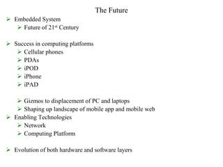
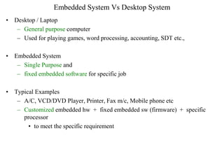
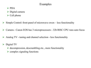
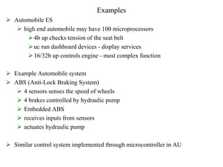
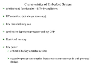
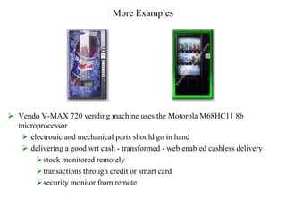
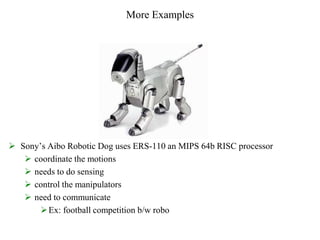
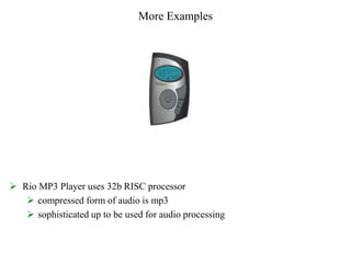
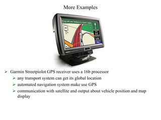
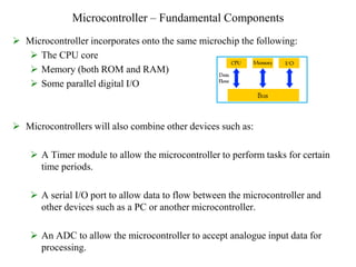
2. The Future
Embedded System
Future of 21st Century
Success in computing platforms
Cellular phones
PDAs
iPOD
iPhone
iPAD
Gizmos to displacement of PC and laptops
Shaping up landscape of mobile app and mobile web
Enabling Technologies
Network
Computing Platform
Evolution of both hardware and software layers
3. History of Embedded Systems
• 1970
– Computers for commercial and admin apps
– Microprocessor – miniaturization – Moore’s Law
• 1980
– Computer networks – bridge IT + Telecommunication
– Mouse, Windows and GUI
• 1990
– Internet and WWW – access to digital technologies
• 2000
– Second revolution for embedded systems
• Economic Challenges
– Increase fuel economy and reduce emissions in automobile by adjusting
motor state
– Airbags and assisted braking systems – improve comfort and security of
passengers
– Improve security, performance, attractiveness and market share
4. Introduction to Embedded System
• System
– Way of working, organizing, performing one or many tasks as per rules or
plan
– Arrangement – units assemble and work together as per program or plan
• Examples of system
– Time display system – watch
– Automatic cloth washing system – washing m/c
• Embedded Systems are
– Omnipresent (homes, office, shopping malls, hospitals, cars, aircraft…)
– Computing Device – does a specific focused job
5. What is Embedded System?
Embedded System
any device that includes a computer but is not itself a general purpose
computer
h/w and s/w - part of some larger systems and expected to function without
human intervention
respond, monitor, control external environment using sensors and actuators
embedding a computer - but not for general purpose
Applied Computer System
Includes analog interface to the external world
6. Embedded System - Definitions
• An embedded system is an application that contains at least one programmable
computer (typically in the form of a microcontroller, a microprocessor or digital
signal processor chip)
– is used by individuals who are, in the main, unaware that the system is
computer-based
» From Embedded C Programming perspective by Michael.J.Pont
• “An embedded system is a system that has software embedded into computer-
hardware, which makes a system dedicated for an application (s) or specific part
of an application or product or part of a larger system.”
– s/w usually embeds into a ROM or flash
– Independent system or part of a large system
» by Raj Kamal
7. Embedded System - Definitions
• “An embedded system is one that has a dedicated purpose software embedded in a
computer hardware.”
» By Raj Kamal
• Any device that includes programmable computer but not self intend to be a general
purpose computer
» Wayne Wolf
• Electronic system contains microcontroller or microprocessor but not general purpose
computers
• computer is hidden or embedded in the system
» Todd D. Morton
• Combination of Software and Hardware in which the software controls the entire
hardware for a dedicated application
» Raj Kamal
• A general-purpose definition of embedded systems is that they are devices used to
control, monitor or assist the operation of equipment, machinery or plant. “Embedded”
reflects the fact that they are an integral part of the system. In many cases, their
“embeddedness” may be such that their presence is far from obvious to the casual
observer.
>> Institute of Electrical Engineers (IEE)
8. Embedded System Vs Desktop System
• Desktop / Laptop
– General purpose computer
– Used for playing games, word processing, accounting, SDT etc.,
• Embedded System
– Single Purpose and
– fixed embedded software for specific job
• Typical Examples
– A/C, VCD/DVD Player, Printer, Fax m/c, Mobile phone etc
– Customized embedded hw + fixed embedded sw (firmware) + specific
processor
• to meet the specific requirement
9. Examples
PDA
Digital camera
Cell phone
Simple Control: front panel of microwave owen – less functionality
Camera - Canon EOS has 3 microprocessors - 32b RISC CPU runs auto focus
Analog TV - tuning and channel selection - less functionality
Digital TV
decompression, descrambling etc., more functionality
complex signaling functions
10. Examples
Automobile ES
high end automobile may have 100 microprocessors
4b up checks tension of the seat belt
uc run dashboard devices - display services
16/32b up controls engine - most complex function
Example Automobile system
ABS (Anti-Lock Braking System)
4 sensors senses the speed of wheels
4 brakes controlled by hydraulic pump
Embedded ABS
receives inputs from sensors
actuates hydraulic pump
Similar control system implemented through microcontroller in AU
11. Characteristics of Embedded System
sophisticated functionality - differ by appliances
RT operation (not always necessary)
low manufacturing cost
application dependent processor and not GPP
Restricted memory
low power
critical in battery operated devices
excessive power consumption increases system cost even in wall powered
devices
12. Characteristics of Embedded System
Manufacturing cost
Non-Recurring Engineering cost (NRE) – cost for design and development
cost of production and marketing each unit
production cost should be taken care when targeting mass market
Ex: AU Versus low cost cell phone
Technology choice depends on no of units plan to produce
13. Characteristics of Embedded System
RT operation
finish operations by deadlines
HRTS - missing deadline is catastrophic
automated missile launch system
SRTS - missing deadline degrades performance
playing video - missed decoded frame
many systems are multi rate - inputs from external world comes at different rates
14. Characteristics of Embedded System
Application dependent requirements
Fault Tolerance and Reliability
continue operation despite hw or sw faults
Ex: aircraft and medical monitoring sys
Safe
avoid physical or economic damage to person or property
15. Characteristics of Embedded System
More Features – Dedicated Systems
Pre-defined functionalities – h/s accordingly designed
Programmability rarely used during life time of system
not programmed on regular basis
OTP and execute infinitely
do specific task
RT, fault-tolerant and safe
16. Characteristics of Embedded System
• Single Functional - cannot be programmed to do different things
– pagers and mobile phones
• Limited Resources - fixed RAM, ROM
– No secondary storage CD-ROM, FDD
• Work against deadlines - Real Time systems
• Missing deadline cause catastrophe
• Power constrained - Battery powered products
• Highly reliable - No 3 finger salute – cannot afford to reset
• Extreme environment conditions - Temperature and humidity
• Cost sensitive to CE - Millions of units sold
• Diversified processors and OS unlike desktop (intel + MS - Wintel)
– complex to chose right platform
17. Constraints in Embedded Systems
Tightly constrained than traditional software systems
• Cost
– Cannot have high end or fast processor
– Cannot have more memory – processor footprint should be less
• Size
– Processor footprint should be less
• Ex: gun stabilization control for Arjuna Tank in Defence
• Cooling requirements + Processor should take less space
• Performance
– Ex: Digital camera snaps, Mobile phone address book contact list etc.,
• Power
– Battery power products – Mobile phones
– Optimized power saving algorithms and operating modes – reduce power dissipation
– SW Program size + # of instructions – affect processor’s energy consumption
• Available System Memory and Processor Speed
• Limited power dissipation when running system continuously
• Reactive and Real Time – Adaptive cruise control and radar missile detection systems
21. More Examples
Vendo V-MAX 720 vending machine uses the Motorola M68HC11 8b
microprocessor
electronic and mechanical parts should go in hand
delivering a good wrt cash - transformed - web enabled cashless delivery
stock monitored remotely
transactions through credit or smart card
security monitor from remote
22. More Examples
Sony’s Aibo Robotic Dog uses ERS-110 an MIPS 64b RISC processor
coordinate the motions
needs to do sensing
control the manipulators
need to communicate
Ex: football competition b/w robo
23. More Examples
Rio MP3 Player uses 32b RISC processor
compressed form of audio is mp3
sophisticated up to be used for audio processing
24. More Examples
Garmin Streetpiolot GPS receiver uses a 16b processor
any transport system can get its global location
automated navigation system make use GPS
communication with satellite and output about vehicle position and map
display
25. More Examples
Miele dishwashers uses 8b Motorola 68HC05 processors and can be
reprogrammed with a laptop to adjust temperatures and cycle times
27. Types of Embedded System
similar to general computing
PDA, video games, STP box, ATM
Since the functionalities is subset of PC functionalities
i/0 based
no sensing of ext environment and no control of actuators
more like general purpose
respond to users input
Control systems
sensing and actuating - is a specific job
feed back control of RT systems
vehicle engines - fuel injection control
flight control
nuclear reactors
28. Types of Embedded System
signal processing
core job is processing of signals
radar
sonar
DVD players
communication and networking
cellular phones,
internet appliances
web enabled vending m/c
29. Nature of System Functions
Functions expected from Embedded Systems – To do
obey control laws - for sensing and actuation
sequencing logic - task specific and not general
signal processing - if there is external interface
may not be a core activity
but required to deal with sensing inputs
app specific interfacing
what kind of sensors and actuators interconnected
h/s interfacing for i/o devices
fault response
what happens if fault occurs
General philosophy is - graceful degradation
Catastrophic failure should not happen
Ex: battery low in mobile phone – message to user before shut down
30. Embedded System Architecture
Memory - has the software to control the system
AD conversion blocks - interface to sensors
DA conversion blocks - interface to actuators
integral and essential component of embedded control systems
31. Embedded System Architecture
FPGA / ASIC
special hw interfaces with CPU
CPU off shores special functionalities
human interface with CPU - LCD, LED
diagnostic tools
trace failures
system does self checks to check all paths on regular basis using diagnostic
tools
if not system may damage the users due to unexpected malfunctions
power cooling systems
proper package of whole systems wrt external environment
good well system can fail due to improper packaging
Ex: moisture controlling
mechanical aspects of design - too critical
32. Implementing Embedded System
HW
PE - uc and up
peripheral devices
i/o
interfacing sensors and actuators
interfacing protocols
Memory
Bus
HW aspects looks similar to general purpose systems
But embedded systems differ by peripherals
General purpose is about std i/o devices
in ES - i/o devices varies a large
diff kinds of sensors - so PE should be defined wrt i/o devices
33. Implementing Embedded System
cross assemblers and compilers
host and target m/c
Ex: compiler for PIC uc on simple PC
compile c program for PIC uc (target board)
not executed on PC in which it is compiled
compilers for family of processors (variants)
since similar architecture but differ by registers or features
emulators
IS emulators
emulates target processor on another m/c
simulation environment
timing analysis of code on host m/c
34. Implementing Embedded System
PC - hw connector - target board
monitor execution of code from PC
debugging tools
System SW
Cross compilers and assemblers
emulators and simulators
debugging tools
System SW aspects differ from that of general purpose system
Top of the system sw is specialized OS with RT features if required
App sw - flavors for different devices
Ex: same os vxworks on laser printer and on other appliances
app sw targeted for printing on top of OS
app sw distinguish the functionality
35. History of HW Evolution
Based on faster clock and degree of integration
GP up and uc
get OTS products and develop system out of it
Development cost (NRE) is reduced by using GP up and uc
DSP
signal processing is the basic task
cost is more than GP
AS processors (ASSP / ASIC)
designing processor that exactly suit application need
development cost is more
application will be an additional cost
SoC
multi cores + Co-Processor + peripherals
Ex: TI - RISC + TI DSP + entire communication integrated
more sophisticated functionalities
36. History of Processor Architecture Evolution
Von-Neumann Architecture
Primitive architecture
Computer programs – small and simple but memory is costly
Program and data stored in same memory
Instruction and data access on same bus from memory
Single bus b/w CPU and memory
RAM and program memory share the same bus and same memory and so must
have same bit width
Each instruction fetched from memory, decoded and executed
On decoding, any operands required fetched from same memory
Bottleneck: getting instructions interfere with accessing RAM
Provide address on bus to fetch instruction as well as data
Use bus to r/w data onto memory
No diff b/w data and instruction
Distinct cycles for getting address and data
Stored program computers
Instructions / programs stored in ROM
No changes at run time
37. History of Processor Architecture Evolution
Harvard Architecture
Separate data paths (address and data buses) – access code (program) and data (data
operands) - Separate program and data bus – buses can be of different widths
Next instruction can be fetched while decoding and executing current instruction =>
Instruction pipelining is easy
Ex: program memory <- 12/14/16b bus -> cpu <-8b bus-> data
memory
program memory different from data memory
two distinct buses b/w CPU and memories
Advantages
fetch instruction from program memory - process data and store processed data
into data memory
fetch next instruction while storing the previous result due to separate memories
and separate buses
facilitates instruction pipelining
fetch instruction and fetch/store data at the same time on different buses
many uc built on harvard architecture
38. History of Processor Architecture Evolution
Harvard Architecture Derivatives
Modified harvard or super harvard architectures
Multiple data paths for data access
More suited for data intensive applications : DSP – require multiple data
operands for each instruction execution
Fetch data operands in parallel using multiple data paths – significantly
improves performance
39. History of Processor Architecture Evolution
CISC – Complex Instruction Set Computer – Intel 8086, Pentium
Earlier application were in machine or assembly code – no HL / MLL
Computer hw supported large instructions – simplify programming – easier and
faster
Instructions do complex operations
Single instruction fetch multiple operands and execute multiple operations on the
operands
Advantages
Made programming easier – less instructions to do given task
Favored for low memory – memory cost is reduced since less instructions to
store
Dense instruction set to reduce memory requirements
CISC – Basic philosophy
Different instructions of different formats, lengths, addressing modes
Require multiple clock cycles for execution
More complex instructions be implemented as part of hw
more elaborated accessing of data as part of instructions
diff addressing modes of accessing data
40. History of Processor Architecture Evolution
RISC – Reduced Instruction Set Computer
CISC complex instructions take many osc cycles to execute
Pipelined processor overall speed depends on the slowest operation being
performed
Relatively complex instructions even slow down the execution of
simpler instructions
complex instructions were a major performance bottle-neck
Advent of compilers and HLL / MLL
Compiler translates HLL code to low level assembly or machine code
Compilers generally used a combination of simple instructions to achieve the
complex operations
breaking the complex operations in to a combination of simple operations
was much efficient
took less processor cycles to execute, than doing the same operations
using a single complex CISC instruction
most of the complex instructions were not being used by compiler
generated programs
41. History of Processor Architecture Evolution
Most of the addressing modes (offered by CISC) were also not being used by
compilers.
This led to a shift in processor design philosophy
Processor designers started focusing on
reducing the size and
complexity of instruction sets
since most complex instructions were not being used and
making a small and simple instruction set - which could be used by
compilers
Advantages
simpler instructions could speed up the pipe-line and thus provide a
performance improvement.
simple instruction set implies less computer hardware and thus reduced cost.
42. History of Processor Architecture Evolution
RISC basic design goals
Less # of instructions – instruction designed for simple operations executed
in single cycle
provide basic simple instructions, which could execute faster.
Compilers could use these instructions to construct complex operations
Each instruction is of fixed length
facilitates instruction pipelining - reading of next instruction byte will
not interfere current instruction being read
Design fetch cycles to fetch words of fixed length corresponds to
single instruction
large # of general purpose register set
contain data or address (symmetry) - used for address and data
manipulation equally
43. History of Processor Architecture Evolution
Load / Store Architecture of RISC
ALU operations always involve registers and not memory locations
no memory access for data processing instructions
load instructions to load data from memory to register
store instructions to store processed data from register to memory
RISC Architecture => referred to as Load/Store Architecture
Implementing pipelining in CISC architecture is more complex than RISC arch
Interesting trend in this era (early eighties)
sharp increase in the speed of processors (whereas the memory speeds still
remained comparatively low)
This meant that memory accesses were becoming a bottle-neck.
This led to the design of processors with large number of internal
registers
used for temporary storage rather than depending on external and
slower memory and cache memories.
44. History of Processor Architecture Evolution
DSP
special purpose processors
processing units and instruction set suit the Signal Processing Applications
MAC (Multiply and Accumulate) and Shifter (Arithmetic and Logical shift) units are
added to the DSP cores
Signal Processing Algorithms heavily depend on such operations
Other common features in DSP architectures
Circular Buffers, Bit Reversal Addressing, Hardware Loops, and DAG (Digital
Address Generators)
Signal Processing Applications are data intensive
the data I/O bandwidth of DSP processors is designed to be high
lot of embedded systems run signal processing applications (cell phones, portable
media players etc)
45. History of Processor Architecture Evolution
VLIW Architecture
“Very Large Instruction Word” architecture consists of multiple ALUs in parallel
designed to exploit the “Instruction Level Parallelism” in application.
Programmers can break their code such that each ALU can be loaded in parallel.
The operation to be done on each ALU (in a given cycle) forms the instruction
word (for that cycle).
It is completely up to the programmer to take care of partitioning of the application
across different ALUs.
Also, it is programmer’s burden (and compiler’s burden if the code is being
written in high level language) to make sure that there is not interdependency
between the instructions with are part of “instruction word”.
The processor does not have any hardware to ascertain (and reschedule) the order of
instructions (this is called static scheduling).
46. Characteristics of Embedded SW
logically and temporally correct programs
cant do correct at wrong time
correct operation has no meaning
deal with inherent physical concurrency
GP m/c - multi users and processes running
ES - physical world is concurrent - have to support concurrency
Reactive Systems
has to be reliability and fault tolerance
has to be app specific and single purpose
47. Multitasking and Concurrency
deal with several i/o and multiple events occurring independently
Many of ES - expected to be multitasking
separating tasks simplifies programming complexity
but requires s/w mechanism for multi-tasking - switching b/w different tasks
concurrency => appearance of simultaneous execution of many tasks
48. Challenges in ES Design
how much hw do we need?
word size of CPU and size of memory
how do we meet our deadlines (deadlines for a RT system)
faster hw or cleverer sw
faster cpu means extra cost
cleverer sw requires faster cpu
so, design logic on FPGA or ASIC a dedicated function using low cost cpu and
include it for compromising on cost
dedicated logic on FPGA or ASIC to compromise of SW so as to meet deadline
how do we minimize power
turn off unnecessary logic
reduce memory accesses
49. ES Design – A Global Picture
multi objective
dependability
not fail
should have fault tolerance or graceful degradation
affordability
depending on the market targeted
safety
security
not cause bodily harms to users
scalability
timeliness
operation in time
50. ES Design – A Global Picture
To meet above multi objectives of ES design we need multi-discipline
electronic hw
mechanical hw
control algorithms
sw
humans
society / institutions
sociological acceptance of product - accept by society
51. ES Design – Life Cycle
ES Design Life cycle events
LC => how do a ES gets developed
Requirements
Design
Manufacturing
Deployment
Logistics of maintaining the system
Retirement support
52. ES Design Goals
performance
overall speed, deadlines
funtionality and user interface
mfg cost
power consumption
phy size etc.,
size and power also related to performance and should be taken care accordingly
Ex: cannot design a digital camera of wt 10 kg
53. ES Design Goals
Functional and Non Functional Requirements part of ES design
Functional requirements
o/p as a function of i/p - specification of ES as i/o
Non Functional requirements
time to compute o/p
size
weight
power consumption
Reliability etc.,
functional and non functional requirements are critical for product acceptance
54. Design and Development Process of ES Life Cycle
Requirements
Specifications
Architecture
Components Design
System Integration
Testing is critical
GP system - patch download for a bug
ES system - use forever and no flexibility for patch update
55. ES Design Approach
TD or bottom up as like SDLC
TD
start from most adt description work to most detailed
BU
work from small components to big system
re-use of parts already developed
real design uses both techniques
stepwise refinement (both h/s development go in hand)
at each level of ADT analyze design to determine characteristics of current
state of the design
refine design to add detail
in ES: since special purpose h/w is designed if deadline not met with SW
so hw and sw design should go in hand
56. Microcontroller
Device
Integrates # of components of microprocessor system on to a single microchip
Optimized to interact with ext world through on-board interfaces
i.e. it is a little gadget that houses a microprocessor, ROM (Read Only Memory),
RAM (Random Access Memory), I/O (Input Output functions), and various other
specialized circuits all in one package.
Microprocessor
Optimised to coordinate flow of information b/w separate memory and
peripheral devices located outside itself
System bus (AB / DB / CB) - up uses to select the peripheral for sx/rx data
Microcontroller
Processor and peripherals on single silicon
Self-contained device – rarely bus structures extend outside package
57. Microprocessor Vs Microcontroller
Microprocessor
Collection of on/off SWI on Silicon
for computations
CPU is stand-alone, RAM, ROM, I/O,
timer are separate
designer can decide on the amount of
ROM, RAM and I/O ports.
Expandable
Expensive
High Speed (1000 MIPS)
General purpose and Versatile
Large Architecture (32b, 64b)
Lots of IO and Peripherals externally
connected
Microcontroller
Small and self-suffice SoC to control
devices
CPU, RAM, ROM, I/O and timer are
all on a single chip
fix amount of on-chip ROM, RAM,
I/O ports
Not Expandable – no external bus
interface
for applications in which cost, power
and space are critical
Low speed, on the order of 10 KHz –
20 MHz
single-purpose
Small usually an 8b
Limited IO, enough for intended app
58. Microcontroller – Fundamental Components
Microcontroller incorporates onto the same microchip the following:
The CPU core
Memory (both ROM and RAM)
Some parallel digital I/O
Microcontrollers will also combine other devices such as:
A Timer module to allow the microcontroller to perform tasks for certain
time periods.
A serial I/O port to allow data to flow between the microcontroller and
other devices such as a PC or another microcontroller.
An ADC to allow the microcontroller to accept analogue input data for
processing.
59. Basic Microcontroller Architecture
Memory Unit
Store data and program
Addressing and memory locations
Control line to r/w
CPU
ALU + CU + Shifter + Memory L/S opns
Processor Registers
Connection b/w memory and CPU
Bus
Wires in power of 2 – address, control and data bus
address bus – wires = amount of memory
data – word length – connect all blocks inside microcontroller
MU + CPU + BUS – self contained unit + no external interface
60. Basic Microcontroller Architecture
External I/O Interface
Block with several memory locations
One end to DB and other end to output lines on uc – pins on IC
Input-output unit
Ports are memory locations
Types of ports : input, output or bidirectional ports.
Working with Port
Select the port
Configure for i/o and r/w data
Ports simply acts like memory locations
61. Basic Microcontroller Architecture
Serial Communication
Parallel data transfer lines affects economy
3 line with protocol preferred
Ex: Serial Protocol – Non Return to Zero
Full Duplex communication
Data transferred serially (bit by bit)
Rx => Data read from received port location and stored in memory
Sx => data from memory via bus to sending port location and to rx unit as
per protocol
Timer Unit
Info about time duration, protocol in serial communication
free-run counter which is in fact a register whose numeric value increments
by one in even intervals – elapsed time calculation b/w time intervals
62. Basic Microcontroller Architecture
Watchdog Timer
flawless functioning of the microcontroller during its run-time
What if uc stops working or works incorrectly due to interference?
PC => reset but ES => no reset button since no human intervention
Watchdog Block - in fact another free-run counter
SW program needs to write a zero in every time it executes correctly.
If SW "stuck", zero will not be written in
counter alone will reset the microcontroller upon achieving its
maximum value.
This will result in executing the program again, and correctly this
time around.
an important element of every program to be reliable without man's
supervision
63. Basic Microcontroller Architecture
Analog to Digital Converter (ADC)
Peripheral signals (voltage) differ from uc signals (binary)
ADC block for conversion
Assembling all the blocks into an electronic component where uc will access
the inner blocks through the outside pins
64. Interrupt
Major diff b/w DTP SW and embedded sw is ‘interrupt’
Low level perspective
hw mechanism for notification to CPU about event occurrence
Internal events: overflow of timer
External events: arrival of char through serial interface
High level perspective
Mechanism for creating
multitasking applications
Apparently performing
>1 task at a time using a single up
Interrupt handling in embedded
system
65. Why 8051?
Price less than $1.00 (US)
1 MIPS performance
256 bytes of on-chip RAM
Profile - price, performance, available memory match needs
8051 architecture - by Intel
Philips, Infineon, Atmel and Dallas
Instruction Set / Code compatible
60% microcontroller market - 50% of the 8-bit microcontroller market
Used in automotive systems to children’s toys
low cost, huge range, easy availability and widespread use of the 8051 family
makes it
an excellent platform for developing embedded systems:
ideal platform for learning about embedded systems.
66. Intel MCS-51 family
Standard 40-Pin DIP pacakage
Excellent device for building embedded systems
Minimum # of external components to operate
67. Choosing a Microcontroller
Meeting computing needs of task at hand efficiently and effectively
Speed – highest speed supported
Packaging – for space, assembling and prototyping of end product
Power consumption – crucial for battery powered products
Amount of RAM and ROM on-chip, # of Timers and IO Pins
How easy to upgrade to high performance or low power consumption versions
Cost per unit
Availability of SDT (Compilers, assemblers, debuggers) and expertise
Wide availability and reliable sources (Source of Suppliers beside Originator)
Intel, Atmel, Philips / Signetics, Infineon, Dallas Semi / Maxim
69. Pin Description
1-8 – Port 1 – bi-directional – individual control of pins as i/o
9 – Reset Pin
Logic 0 – normal run mode of chip
Logic 1 - >= 2 machine cycles – reset chip
10-17 – port 3 – bi-directional input port
Dual role of individual pins
P3.0 – RXD – receive serial data
P3.1 – TXD – transmit serial data
P3.2 and P3.3 – process external interrupts
P3.4 and P3.5 – Alternative functions of T0 and T1
P3.6 and P3.7 – r/w signals for external memory
18-19 – external crystal, ceramic resonator or oscillator module for clock source to the
chip
20 – Ground Vss
21-28 – Port 2 – bi-directional input port
Dual role - MSB address byte of 16b address to external memory
29 – PSEN – control access to external code memory
30 – ALE –
When working with external memory
Disabled to reduce EMI generated by the product
Also used as PROG – program pulse input during flash programming
31 – EA
Connected to Vcc to execute code from internal memory (on chip flash)
Connected to ground to execute code from external memory
32-39 – Port 0 – bi-directional input port
Does not have internal pull-up resistors
Dual role – gives LSB address byte of 16 address to external memory
40 – Vcc – 5V pin
70. Memory Issues relating to 8051
Types of memory
Computer tapes –access time varies for r/w wrt location on tape
RAM – volatile r/w memories
Same time for accessing any random memory element
ROM – random access but non volatile
DRAM
r/w memory
Capacitor along with active elements to store data
Circuit to refresh capacitor frequently for retention
Volatile
SRAM
r/w memory
Use FF (active elements) to store information
No refreshing
Circuit is Costly than DRAM of same size
Access time is 1/3 rd of DRAM
71. Memory Issues relating to 8051
Mask ROM
RO from s/w developer perspective
Manufacture able to write at the time of chip creation according to mask given by
company
Factory programmed ROM
Not cheap and not an option of low volume
Mistakes are expensive
Providing code for first mask is like character building process
Slower access times than DRAM
8051 members with on chip, mask programmed ROM are available
PROM
WORM (write once read only memory) or OTP
PROM programmer – blow tiny fuses in the memory device
Fuses blown cannot be repaired but devices are cheap
Modern 8051 variants include OTP ROM
72. Memory Issues relating to 8051
UV EPROM
Programmed electrically
Has quartz window to erase memory by exposing the device to UV light
Erasure takes several minutes
Quartz window covered with UV opaque label after erasure
Can withstand 1000’s of program / erase cycles
Useful for prototyping but expensive to use in production
More Flexible than PROM and rather primitive compared to EEPROM
8051 members with on board UVEPROM are available
EEPROM and Flash ROM
More user friendly form of ROM
Can be both Programmed and erased electrically
EEPROM erasure is byte-by-byte basis – used to store password or persistent user data
FLASH ROM requires block sized erase operation before programming
Size of block in order of several KB
Used for storage of program code
Many 8051 members have onboard EEPROM and Flash both
73. Memory Organization and hex
All data items in memory => binary codes in bits form
Memory locations with address => simplify storage and retrieval of data items
Byte oriented memory => each memory location has a byte with unique address
Memory addresses in hex notation
Hex – base-16 number system – compact way of representing large binary
numbers
Table shows list of # with hex, ordinary and binary representations
74. 8051 Memory Architecture
• 8051 – 128 Bytes of RAM (00H- 7FH)
• RAM memory space allocation
– 32 bytes (00H – 1FH) – register banks and stack
– 16 bytes (20H – 2FH) – bit addressable r/w
memory
– 80 bytes (30H – 7FH) – Scratch pad
• Data and parameters of 8051 programs
• Data Memory
– Store data variables and stack while program runs
– implemented using some form of RAM
– byte-oriented memory organization
– within the DATA area is a 16-byte BDATA area
which can also be accessed using bit addresses
• used to store bit-sized variables
• has machine instructions which allow bit
variables to be manipulated very efficiently
• instructions can be easily utilized from C
7FH
30H
2FH
20H
1FH
17H
10H
0FH
07H
08H
18H
00H
Register Bank
0
(Stack)
Register Bank
1
Register Bank
2
Register Bank
3
Bit-Addressable
RAM
Scratch pad RAM
75. 8051 - CODE Memory
• 8051 – 4K bytes of on-chip ROM
• Store program code – usually in some form of ROM
• May contain read-only variables (‘constants’)
– such as filter co-efficients or data for speech playback
• DTP PC Context
– Program copied from Disk to RAM
– Executed from RAM
• Embedded System Context
– code is ‘executed in place’, from ROM
–
• Consequence of the ‘execute in place’
– most applications, may require up to 10 kbytes of CODE memory, will rarely need
much DATA memory
– Many 8051 - > 20 bytes On-Chip ROM + not >= 256 bytes of RAM
• appropriate mix for most general applications
76. Timers
• Atleast 2 Timers – T0 and T1 (8052 – additional Timer T2)
• 16b Timers – hold (0 -65535) values
• Incremented periodically: 8051 - every 12 osc cycles
• 8051 OSC – 12MHz => 1 million increments per second
• Used to
– measure intervals of time
• For example, we can measure the duration of a function by comparing
the duration at begin and end
– generate precise hardware delays
– generate ‘time out’ facilities - a key requirement in systems with real-time
constraints
– generate regular ‘ticks’, and drive an operating system
77. Interrupts
• Fundamental difference b/w DTP SW and
Embedded SW
• low-level perspective
– hardware mechanism to notify a
processor that an ‘event’ occurs
– Internal events (overflow of timers) or
– External events (arrival of char through
serial interface)
• high-level perspective
– mechanism for creating multitasking
applications
• App performing more than one
task at a time using a single
processor
78. 8051 Interrupt Sources
• 8051/8052 – support 7 interrupt sources
– two or three timer/counter interrupts (related to Timer 0, Timer 1 and – in the
8052 – Timer 2)
– Two UART-related interrupts
• share the same interrupt vector - viewed as a single interrupt source
– Two external interrupts
– In addition, there is one further interrupt source over which the programmer
has minimal control
• The ‘power-on reset’ (POR) interrupt
79. Serial Interface
• 8051 - serial port compatible with RS-232 communication protocol
– transfer data b/w 8051 and desktop PC/notebook PC or similar
– Serial interface is common in embedded processors and widely used
• The serial port may be used to
– debug embedded applications, using a desktop PC
– load code into flash memory for ‘in circuit programming’ (ISP)
• when code must be updated ‘in situ’ (for example, when the product is
already installed in a vehicle, or on a production line)
– transfer data from embedded data acquisition systems to a PC, or to other
embedded processors
80. Timers and Counters
crucial component of most embedded systems.
In some cases, a timer measures elapsed time (counting processor clock
ticks)
In others, we want to count or time external events.
The names counter and timer can be used interchangeably when talking about
the hardware.
The difference in terminology has more to do with how the hardware is used in a
given application.
Both differs largely by their use and not in logic
81. A Simple Timer / Counter
simple timer similar to those often included on-chip within a microcontroller
build something similar from a couple of 74HC161 counters or a programmable logic device.
The timer shown consists of a loadable 8-bit count register, an input clock signal, and an output
signal
Software loads the count register with an
initial value between 0x00 and 0xFF.
Each subsequent transition of the input
clock signal increments that value.
When the 8-bit count overflows, the output signal is asserted.
The output signal may thereby trigger an interrupt at the processor or set a bit that the processor can
read
To restart the timer, software reloads the count register with the same or a different initial value.
If a counter is an up counter, it counts up from the initial value toward 0xFF.
A down counter counts down, toward 0x00.
Start counter usually by setting a bit in a control register
real counter would generally also provide a way for the processor to read the current value of the
count register at any time, over the data bus
82. Semi-Automatic Timers
A timer with automatic reload capability
will have a latch register to hold the count written by the processor
Initial value as starting point
When the processor writes to the latch, the count register is written as well
When the timer later overflows,
it first generates an output signal
then, it automatically reloads the contents of the latch into the count register
Since the latch still holds the value written by the processor, the counter will begin
counting again from the same initial value
Such a timer will produce a regular output with the same accuracy as the input clock.
This output could be used to generate
a periodic interrupt like a real-time operating system (RTOS) timer tick,
provide a baud rate clock to a UART, or
drive any device that requires a regular pulse.
83. Semi-Automatic Timers
Initial value as end point
timers uses the value written by the processor as the endpoint rather than the
initial count
In this case, the processor writes into a terminal count register that is
constantly compared with the value in the count register
The count register is always reset to zero and counts up
When it equals the value in the terminal count register, the output signal is
asserted
Then the count register is reset to zero and the process repeats
The terminal count remains the same
Initial Value or Terminal Value
The overall effect is the same as an overflow counter.
A periodic signal of a pre-determined length will then be produced.
84. Software Configuration for Timer modes
If a timer supports automatic reloading, it will often make this a software-
selectable feature
To distinguish between a count that will not repeat automatically and one that
will, the hardware is said to be in one of two modes:
one-shot or periodic
The mode is generally controlled by a field in the timer's control register
85. Input Capture Timer
has a latch connected to the timer's count register
timer is run at a constant clock rate (usually a derivative of the processor clock )
so count registers is constantly incrementing (or decrementing, for a down counter)
On an external signal
latches the value of the free-running timer into the processor-visible register and
generates an output signal (typically an interrupt)
86. Input Capture Timer
Use for:
to measure the time between the leading edge of two pulses.
By reading the value in the latch and comparing it with a previous
reading, the software can determine how many clock cycles elapsed.
In some cases, the timer's count register might be automatically reset just after its
value is latched
If so, the software can directly interpret the value it reads as the number of
clock ticks elapsed
input capture pin can usually be programmed to capture on either the rising or
falling edge of the input signal.
87. Bus Based Computer Systems
Created using up, IO devices and memory components
Up is vital components of embedded computing system
Cannot do job without IO devices and memories
How interconnect up and devices using cpu bus
Similarities in bus b/w platforms required for different applications – general
useful principles from basic concepts of bus
To Know
Cpu bus – back bone of hw system
Memory – important component of embedded platforms – types of memory
devices
Varieties of IO devices types
Basic techniques for interfacing memories and IO devices to the cpu bus
Structure of complete platform
Development and debugging
System level performance analysis for bus based systems
Alarm clock design example
88. The CPU Bus
Computer system
encompasses much more than CPU
also includes memory and IO devices
Bus – mechanism by which cpu communicates with memory and IO devices
Bus
collection of wires + also defines protocol by which cpu, memory and
devices communicate
Major role of bus – to provide interface to the memory and IO devices
Characteristics of memory and IO device components is important
89. Memory issues in Embedded Systems
Modern microprocessors do more than just read and write a monolithic memory.
Architectural features improve both the speed and capacity of memory systems.
Microprocessor clock rates are increasing at a faster rate than memory speeds
memories are falling further and further behind microprocessors every
day.
computer architects resort to caches to increase the average performance of
the memory system.
Although memory capacity is increasing steadily, program sizes are
increasing as well, and designers may not be willing to pay for all the
memory demanded by an application
90. Memory – Bus – Design Factors
Functional aspects of memory
Bus + Protocol
Memory + Controller
Factors for designing memory subsystem
Speed
Capacity or Size (not physical size)
Cost
91. Memory Classification
Based on holding data
Hold data irrespective of power => Volatile and Non-Volatile
Volatile => memory contents erased when the power goes off
Non – Volatile => memory holds contents (data) even if power is not there
Ex: Magnetic Tape
does not require power all the time to store the data
contents available even if power is off
volatile still can be used as back up
Functional perspective of Memory SS
ROM and RAM - RO and R/W
RO
CPU place the address and it can only send read control signal
content of the address location is passed on data bus
R/W
random access
any location in memory can be accessed at the same rate
same rate => time to place address and get the data is going to be same for all
the locations in memory, so it can be randomly accessed
counter part of random access is serial access => block by block or byte by byte
so in serial access time taken to access is < n+1th block
92. Memory Classification
Semiconductor based Memories
Ex: all RAM / ROM subsystems comes under this classification
since they make use appropriate semiconductors for storage
Contrast to semiconductor memory is magnetic tape
Magnetic Tapes are used solely for storage purpose
Farther away from CPU compared to other memories
closer to CPU is Memory and farther to CPU is Tape or any storage systems
Based on how exactly data stored
Static RAM
Principle: Current flow exists through some active element as long as
power exists
Fast but costly
Dynamic RAM
Passive element along with active element
Memory controller to take care of memory retention in passive element
Slow with higher capacity and less cost
93. Memory Hierarchies
Memory Hierarchy basically comes from
Speed mismatch b/w CPU and Memory System
Principle of Locality and focus on
Increasing the processor utilization
Speed - Size or Capacity - Cost are in linear relation
Fast, Medium and Slow Memories by dividing entire address space into sections
Fast Memory – Cache – SRAM – easy and peak access – less size
Medium Memory – Main Memory – RAM – DRAM – medium size
Slow Memory – storage subsystems – Tapes or HDD – CPU may not directly access
- larger size
Ex: 1KB cache - 1GB RAM - 1TB HDD
Ensure that CPU always access only the faster memory in order to keep the processor
utilization always up
CPU essentially access the cache – so entire address space will not used by same kind
of memory
94. Cache
SRAM – Closest – Fastest – Costlier - Less Size
Ex: 1KB Cache
Caches are widely used to speed up memory system performance
Many microprocessor architectures include caches as part of their definition
cache speeds up average memory access time when properly used
increases the variability of memory access time
accesses in the cache will be fast,
while access to locations not cached will be slow
cache is a small, fast memory that holds copies of some of the contents of main
memory
Because the cache is fast, it provides higher-speed access for the CPU
But since it is small, not all requests can be satisfied by the cache, forcing the
system to wait for the slower main memory
95. Multi Level Caches
Modern CPUs may use multiple levels of cache
A Two Level Cache System is shown
The first-level cache (commonly known as L1
cache) is closest to the CPU