
Recommended
More Related Content
Similar to Integrated Yield Management Solutions
Similar to Integrated Yield Management Solutions (20)
Integrated Yield Management Solutions
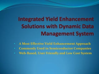
- 1. • A Most Effective Yield Enhancement Approach • Commonly Used in Semiconductor Companies • Web-Based, User Friendly and Low Cost System
- 2. ABOUT US: 75+ years of combined industrial experiences Former Yield Enhancement Specialists from Motorola, Freescale, and Intel. Hands-on experiences in device, processing, yield enhancement, simulation, and software development and manufacturing . A dynamic yield enhancement system based on years of industrial wafer fab development and optimizations. Bilingual Capability Fluent in verbal and written Chinese and English.
- 3. SERVICES: Provides the best solution for yield enhancement infrastructures A comprehensive yield enhancement system with years of industrial optimizations and modifications. Integrated solutions with your existing structures. On-site training for in-house capability. Trouble Shootings Consulting for best practices and solutions of yield related problems.
- 4. SOLUTIONS: Integrated Yield Enhancement System A complete alignment with manufacturing activities. Self-improving cycles for continuing improvement. Dynamic Data Management System Standarized data system for easy access. Centralized data warehouse for multi-dimensional data analysis. User friendly with web-based data analysis and data presentations.
- 5. BENEFITS WE BRING: Most Effective Way to Establish Industry Standard Yield Enhancement System. A complete alignment with manufacturing activities. Self-improving cycles for continuing improvement. Lower Product Cost and Stay Competitive Standarized data system for easy access. Centralized data warehouse for multi-dimensional data analysis. User friendly with web-based data analysis and data presentations.
- 6. FEE-BASED SERVICE Web based and face-to-face consultations. Processing flow review. Yield-limited factor analysis. Identify critical defect inspection points. Recommendations and set up for defect inspection tools. Recipe optimizations for improving defect detection rate. Statistical Process Control(SPC) charts and Out of Control Plan (OCAP) Set up Design of line monitor for baseline process flow Kill Ratio(KR) and Potential Yield Loss (PYL) analysis
- 7. FEE-BASED SERVICE Set up bitmapping capability Failure analysis Partitioning experiments Excursion control (containment vs. root cause solution). Trouble shooting Industry best practice Risk analysis and action plans for new process change: Failure Mode and Effects Analysis (FMEA), Change Action Review system.
- 8. Integrated Yield Enhancement & Dynamic Data Management System
- 9. Keys Terminologies Killer Defect (KD): The defect has certain impact of causing final dies fail. Kill Ratio (KR) = 1/number of killer defects may cause a die fails. KR is a number between 0 and 1, and is associated with a certain type of defect at a certain processing step. (e.g. particle over 0.5 mm size would have KR of 0.5 at the post W CMP) Potential Die Loss (PDL) = NKD* KR. For KR of 0.5, PDL is 5 if KD is 10 at the inline inspection. Potential Yield Loss (PYL) = 100*(PDL/number of dies). PYL is 1% if PDL is 5 with a production wafer with 500 dies.
- 10. Integrated Yield Enhancement System Wafer Inline Parametric Functional Failure Processing Inspections Probe Probe Analysis Wfr. Tool Recipe Process Tracking Quals Quals Processing Info. Modification & (PROMIS) Improvements Defect Images Others Inspections (AIT, (SEM, (EDS, VC, KLA, Compass) Optical) FIB) Inline Probe EOL Probe Post-Stress Inline Inspection & Testing (C1, C2, ..) ( products & Line Test Establishing Kill Ratio Monitors) (KR) Initial Post-Stress Probe Probe (Sort 2) Potential Yield Loss (Sort 1) TEM, SEM, Auger, Bitmapping Customer FIB, Voltage Returns Contrast Failure Analysis Verification of Top Failure Mechanisms